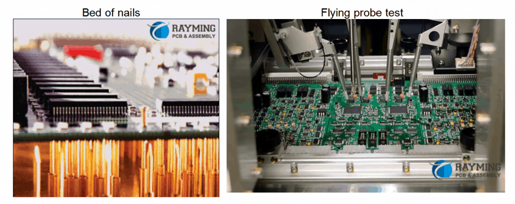
A bed of nails test fixture refers to a type of printed circuit board (PCB) testing jig populated with an array of spring-loaded “nails” used to make electrical connections with circuits during quality control functional testing procedures. These fixtures allow engineers to rapidly validate assembled PCBs for manufacturing defects and verify proper performance before shipment to customers.
Some key things to know:
- Provides quick access to test nodes on a PCB under test (BUT)
- Uses array of pogo pins to contact circuits
- Checks for errors like opens, shorts
- Confirms circuit logic functionality
- Essential tool for PCB quality control
Below we dive deeper into common bed of nail testing applications, fixture configurations, pogo pin specifics, usage methodology and advantages over other test options.
Typical Applications of Bed of Nail Test Fixtures

Bed of nails fixtures are versatile tools utilized for various PCB inspecting and debugging operations:
End-of-Line Quality Testing
Most commonly, bed of nails rigs are leveraged as critical end-of-line quality control stations in PCB assembly lines to catch errors before shipping products to clients.
Design Verification
During PCB prototyping and design verification, bed of nails provides rapid connectivity to validate board circuit integrity, functionality and performance meets specifications.
To diagnose problems with faulty boards pulled from production or returned from field failures, bed of nails testing aids engineers investigating bug root causes.
Focused Functional Test
For more extensive PCB testing needs, bed of nails jigs are often used in tandem with flying probe testers to access targeted test nodes.
Next we’ll explore popular bed of nails configuration options…
Bed of Nails Fixture Designs
Bed of nail test jigs utilize a wide array of spring-loaded pins to contact test points on PCBs. But beyond the basic pogo pin bed, there are several tester designs tailored to application needs:
Standard Grid Array
The most common simple design houses pogo pins in a regular grid array of rows and columns in a plate. This works well for many boards.
Custom Layouts
For odd board shapes and sizes or tricky access points, fully custom nail placements tailored to match PCB test pad locations optimize test coverage.
Clamshell Fixtures
Clamshell testers utilize hinged top and bottom pogo pin jig plates closing over boards like a clamping cradle. This allows access to both sides of boards.
Flying Probe Hybrids
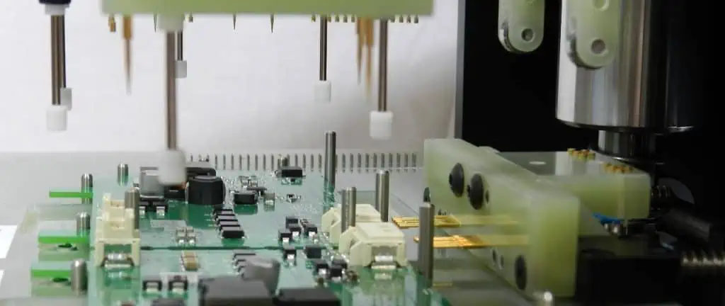
Some bed of nails integrate movable flying probes on x-y axes to reach difficult test nodes that would be impractical to access with fixed nail positions.
Minimal Fixtures
For simple boards, “micro” bed of nail fixtures with small matrices of pogo pins are offered to reduce setup costs when only a few nodes require validation.
Bed of Nails Jig Pogo Pins Overview
The pogo pins embedded in bed of nails testers which make electrical connections to PCBs during in-circuit testing are available in a range of styles. Factors like:
- Pitch – Vertical spacing between pins
- Travel – Compressive stroke length
- Current rating – Rated electrical current capacity
- Precision – Tip positional accuracy
- Durability – Expected test cycles before failure
All impact fixture selection for target board needs. Precision machined pins with long cycle life, gold plating and fine tips offer premium performance.
Using Bed of Nail Fixtures for PCB Testing

The general procedure for utilizing a bed of nails PCB test jig involves:
1. Fixture Programming
- CAD import and nail mapping
- Establishing test protocols
2. PCB Loading
- Properly positioning board into fixture
- Confirming adequate nail contact pressure
3. Test Execution
- Running through test sequence
- Monitoring for passed/failed checks
4. PCB Unloading
- Removing board when sequence finishes
- Checking for pin imprints indicating pressure issues
Fixtures connect to external test equipment suites allowing engineers to define custom check routines to validate correctness of circuits based on board design rules.
Why Use Bed of Nail Test Fixtures?
Bed of nail PCB inspection provides unique advantages over alternatives:
Rapid Access to Test Points
Nails map directly to target test nodes for easy access without requiring extensive wiring hookups to board interfaces. Greatly accelerates and simplifies checking procedures.
Adaptable Configurations
Arrangement of nails can be readily customized to optimize contacting difficult nodes on any board geometry. Hybrid flying probes expand flexibility.
Scalable Testing
Small micro fixtures minimize startup costs for simple PCBs while standard plates scale to test very dense, complex boards housing thousands of nails.
Opens/Shorts Detection
Array of spring pins allows systematically checking continuity across circuits to uncover manufacturing faults like solder bridges or damaged traces/vias.
Validating Operation
Beyond electrical faults, bed of nails facilitates functionally exercising boards with test pattern stimuli to confirm intended performance.
In summary, this versatile fixture technology remains indispensable for streamlining PCB testing processes while delivering the test coverage needed to catch assembly issues before products ship.
Bed of Nails Testing Challenges
For their many benefits, bed of nails rigs also come with some inherent challenges to factor:
Accessibility Limitations
Dense boards with components on both sides can create node access difficulties. Flying probes help reach tricky spots.
Contact Intermittency
Insufficient pogo pin stroke or force can yield occasional opens during testing. Fixture tuning and maintenance helps.
Dense Pin Fields
Very dense test nail arrangements with fine pitch can suffer from shorts between neighboring pins requiring insulation.
Custom Fixturing Overhead
Specialized application-specific nail mapping and programs for unique PCB designs can increase test development costs.
Precision Maintenance
Keeping fixtures calibrated and pins properly adjusted requires ongoing diligence to prevent false failures or marginal contacts.
Bed of Nails Testing – Frequently Asked Questions

How does bed of nails PCB testing work?
An array of spring-loaded “nails” embed into a plate, making electrical connections when a PCB under test is lowered onto the fixture. Continuity checks and test signals then exercise board circuits to uncover faults.
What are bed of nails fixtures made of?
The plates housing pogo pins are made from materials like aluminum or plastics able to undergo continual compressions without warping. Pogo pins themselves utilize alloys like beryllium copper with gold plating.
What kind of test equipment is used with bed of nails?
The fixtures interface with external tester boxes or PC interfaces running software to orchestrate checking routines. These generate signals sent through nails into circuits with pass/fail threshold detection.
How are bed of nails fixtures customized to PCBs?
Mapping programs import board CAD layouts to optimally organize nail positions for accessing target test nodes. Software tailors test routines to match PCB design rules and functionality.
How often do bed of nail fixtures need maintenance?
Fixtures demand regular inspection of pins for wear along with occasional recalibration and adjustments to ensure pins make solid contact. Pogo pins typically withstand 100,000+ compression cycles before needing replacement.
