Printed circuit boards (PCBs) are essential components in all types of electronic devices and equipment. Designing, manufacturing, assembling, and testing PCBs involves a host of specialized terminology spanning electrical engineering, materials science, fabrication processes, and quality control.
This article provides an overview of common PCB terms you are likely to encounter as an electronics engineer or as part of the PCB supply chain. Understanding the key terminology is helpful for effective cross-functional collaboration and communication.
PCB Design

These terms relate to the schematic capture and board layout stages of the PCB design process:
- Netlist – Connectivity list specifying the interconnections between components.
- Bill of materials (BOM) – Listing of all components to be placed on the PCB.
- Footprint – Physical size and layout of the solder pads and connections for a component on the PCB.
- Schematic capture – Creating the circuit schematic diagram using CAD software.
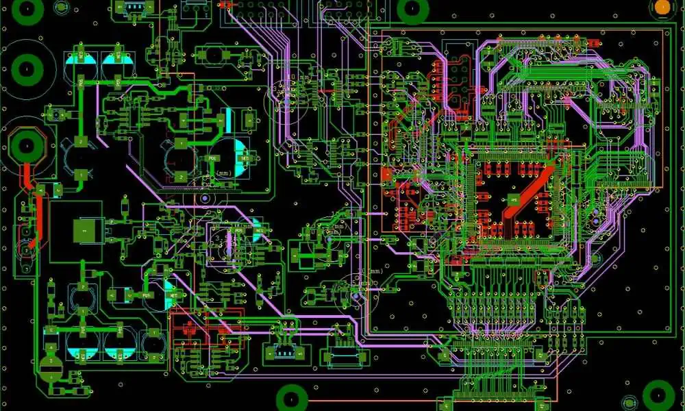
- Layout – Physical positioning and routing of traces to form the board layout.
- Routing – Connecting component pins together with copper trace “wires”.
- Via – Plated through hole connecting between layers in a multilayer PCB.
- Plane – Continuous copper area on a layer, usually for power or ground.
- DRC – Design rule check to validate manufacturability.
- Gerber file – Standard file format for PCB fabrication data.
PCB Materials
These terms refer to the base materials that make up the layers of a PCB:
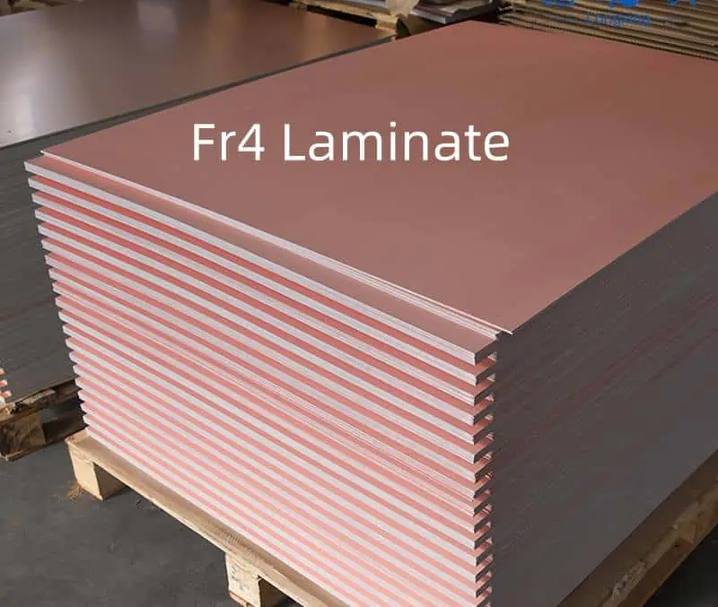
- Substrate – The base insulating material upon which circuits are formed. Usually FR-4 fiberglass.
- Prepreg – Fiberglass sheet impregnated with resin, used between layers in multilayer boards.
- Copper foil – Thin copper layer laminated onto the substrate to form circuits.
- Core – Central substrate layer in a multilayer board with built-up layers on either side.
- Resin – Epoxy polymer that provides the adhesive to bond layers together.
- Weave – Fiberglass reinforcement pattern, like plain weave or tighter weaves for rigidity.
- Dielectric – Insulating substrate material between conductors. FR-4’s dielectric constant is around 4.
- Lamination – Process of bonding foil and prepreg layers together under heat and pressure.
PCB Fabrication
These terms cover processes performed by the PCB manufacturer to fabricate the boards:
- CAM – Computer aided manufacturing file conversions and tooling.
- Etching – Chemical removal of unwanted copper not protected by resist mask.
- Photoresist – Light-sensitive masking material to form the circuit patterns.
- Tenting – Covering up through-hole vias with resist during etching.
- Solder mask – Green epoxy layer that protects copper traces from solder bridges.
- Silkscreen – White epoxy legend layer for markings like component designators.
- Plating – Electrolytic plating of copper in holes and on surfaces.
- Panel – Large board format containing multiple PCBs before singulation.
- Buried via – Via connection within the PCB, not going to an outer layer.
- Blind via – Via starting on an internal layer, not going fully through PCB.
- Impedance control – Methods like smaller trace sizes to match desired impedance.
PCB Assembly

Terms involved in populating a bare PCB with components:
- SMT – Surface mount technology for soldering small components directly to pads.
- Through-hole – Leaded components inserted into plated holes before soldering.
- Pick-and-place – Automated machine placing surface mount parts onto pads with precision.
- Reflow – Soldering SMT parts by heating the entire board above liquidus temperature.
- Wave soldering – Passing boards over a wave of molten solder to solder through-hole parts.
- Hand assembly – Manual soldering of components using an iron, for rework or low volumes.
- Cleanliness – Keeping PCBs free of particles to prevent defects like shorts.
- ECO – Engineering change order to modify the board design or BOM.
- FOD – Foreign object debris that can cause assembly issues.
PCB Parameters
Key specifications and parameters that characterize a PCB:
- Layers – Number of copper layers, typically 2 to 20+ in multilayer boards.
- Thickness – Total thickness of the board in mm or mils. Controlled by layer stackup.
- Aspect ratio – Ratio of total thickness to minimum trace/space width.
- Pitch – Center-to-center spacing between pins or traces.
- Track/Trace – Conducting copper circuit between nodes.
- Space – Gap between adjacent traces on a layer.
- Line width – Width of a trace, often matched to impedance.
- Annular ring – Copper pad area surrounding a drilled hole.
- Finished hole size – Diameter of drilled hole after plating.
- Tolerance – Allowable variation in parameters like hole size.
- Clearance – Minimum distance between copper features on same layer.
- Mask expansion – Solder mask pullback from copper edge.
PCB Testing

PCBs undergo inspection and electrical testing to validate quality:
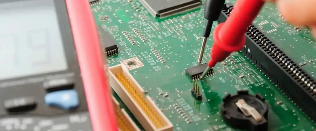
- Flying probe – Automatic test system with movable probes contacting test points.
- Bed-of-nails – Fixture with fixed test probes corresponding to PCB layout.
- Boundary scan – Built-in IC testing through a standard serial interface.
- ICT – In-circuit test system to verify individual components on an assembled board.
- Functional test – Validating complete PCB performance with firmware and load conditions.
- ATE – Automated test equipment systems for high volume production testing.
- Go/no-go – Basic pass/fail criteria for a test step.
- False call – Incorrect test failure result due to measurement inaccuracies.
- Fault coverage – Percentage of possible faults detected by a test regimen.
- Golden board – Unit verified as defect-free to reference against.
PCB Quality and Reliability

Maintaining quality levels and reliability throughout the PCB lifecycle:
- Process capability – Cpk metrics assessing if a process meets specifications.
- Process control – Monitoring processes for statistical control and continuous improvement.
- Yield – Ratio of good boards to total boards manufactured.
- DPPM – Defects per million, a metric for process quality.
- Escape – Defect making it through manufacturing to field failure.
- RoHS – Restriction of Hazardous Substances in electronic equipment.
- Reliability – Probability a PCB functions for its intended lifetime.
- Qualification – Process to validate a PCB for use through accelerated testing.
- FAI – First article inspection of the initial production unit.
- DER – Deliverable exception report if deliverables don’t meet requirements.
- Corrective action – Steps taken to resolve defects and nonconformances.
PCB Repairs and Modifications

PCBs sometimes need fixes or design changes after initial production:
- Re-spin – Iterating board layout to a new version to fix issues.
- Errata – Published documentation of board issues.
- Jumpers – A wire workaround to fix faulty board traces.
- Removal – Using wick or solder pump to remove solder and components.
- Reballing – Replacing solder balls under a BGA package.
- Editing – Modifying the PCB by cutting traces or adding jumper wires.
- Rework – Specialized work like component removal and replacement using hot air tools.
- Focused IR – Using infrared heaters to locally heat specific areas.
- Board handling – Using fixtures, frames, and rails for safe board manipulation.
Conclusion
In summary, PCB terminology spans a wide gamut covering electrical design, fabrication, assembly, testing, quality control, and reliability aspects. As you gain more exposure to PCB engineering, these terms will become increasingly familiar. Referring back to this glossary can help refresh your memory of key PCB vocabulary.
Frequently Asked Questions
Here are some common questions about PCB terminology:
Q: What are some key terms related to the PCB design process?
A: Important PCB design terms include netlist, bill of materials, footprint, schematic capture, layout, routing, via, and plane.
Q: What are some of the materials that make up a PCB?
A: PCB materials include the substrate, prepreg, copper foil, core, resin, fiberglass, and solder mask. The materials determine properties like flexibility and impedance.
Q: What are the main processes used to fabricate a PCB?
A: Key fabrication processes are lamination, photolithography, etching, drilling, plating, solder mask, and silkscreen printing. These transform the materials into a functional board.
Q: What are some ways PCB assemblies are tested?
A: PCB testing methods include flying probe, bed of nails fixtures, boundary scan, in-circuit test, functional test, and automated test equipment.
Q: How are quality and reliability characterized for PCBs?
A: Metrics like process capability, yield, defects per million, field failure rate, and results of qualification testing help quantify PCB quality and reliability.

