Switches are essential components in a wide variety of electronic devices and equipment. They allow the user to control and interact with the system. The two main ways switches are mounted and integrated on printed circuit boards are:
- PCB Mount
- Plate Mount
Each method has its own set of advantages and disadvantages. Selecting between PCB or plate mounted switches depends on factors like cost, ease of assembly, durability, and customization needs.
This article provides a detailed comparison between PCB and plate mounted switches to help design engineers choose the optimal switch mounting scheme for their application.
Overview of Switches
Switches are electro-mechanical devices that interrupt or redirect the flow of current in a circuit to control electrical signals and power. Some common types of switches include:
- Push button switches
- Rocker switches
- Toggle switches
- Rotary switches
- Slide switches
- Tactile switches
- Membrane switches
Switches may have multiple poles with one or more throws/positions. Poles refer to the number of separate circuits the switch can control. Throws indicate the different switching states or routes enabled by the switch.
Some key parameters that characterize switches:
- Number of poles and throws
- Actuation force and travel
- Electrical rating – voltage, current
- Mounting style – PCB or panel
- Termination – leads or connectors
- Size and dimensions
- Enclosure sealing for protection
Understanding application needs and specifications guides selection of the appropriate switch type and mounting method.
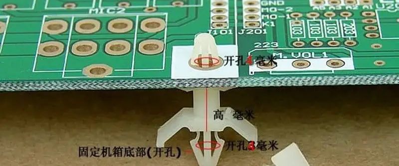
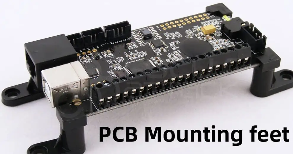
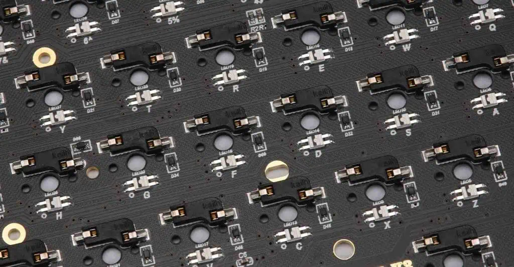
PCB Mounted Switches
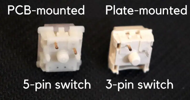
PCB mount switches, as the name suggests, are mounted directly onto a printed circuit board. The switch terminals are soldered to pads on the PCB to integrate them into the circuit.
Some common types of PCB mount switches:
Tactile Switches
- Compact tactile feedback buttons
- Commonly SPST (single pole, single throw)
- Used in consumer electronics, instruments
DIP Switches
- Groups of small sliding switches
- Allows preset configurations
- Used for setting hardware options
Right Angle Switches
- Larger pushbuttons mounted vertically
- Common in industrial controls and machinery
Benefits of PCB Mounting
- Simpler assembly – Switches solder directly to PCB without additional mounting hardware.
- Compact design – No need for added plates or spacers; ideal for small form factors.
- Cost effective – Leverages existing PCB with no other components required.
- Customizable – Switch height, solder pads, and silkscreen legends can be customized.
Drawbacks of PCB Mounting
- PCB area consumed – Switch footprints take up room on the PCB.
- Limited options – PCB mount switches tend to be smaller types with lower electrical ratings.
- Accessibility constraints – PCB location may make switch difficult to access after assembly.
- No labeling – Difficult to add port or function labeling for the switches.
- Vulnerable to board stresses – PCB flexing can damage or crack solder joints.
Applications of PCB Mounted Switches
Some common applications using PCB mounted switches include:
- Small consumer electronics – phones, media players, game controllers
- IoT and wearable devices
- Computer motherboards and peripherals
- Instrument and test equipment front panels
- Industrial control boards
PCB mounting is advantageous where compact form factor is critical or simplicity of manufacturing assembly is preferred.
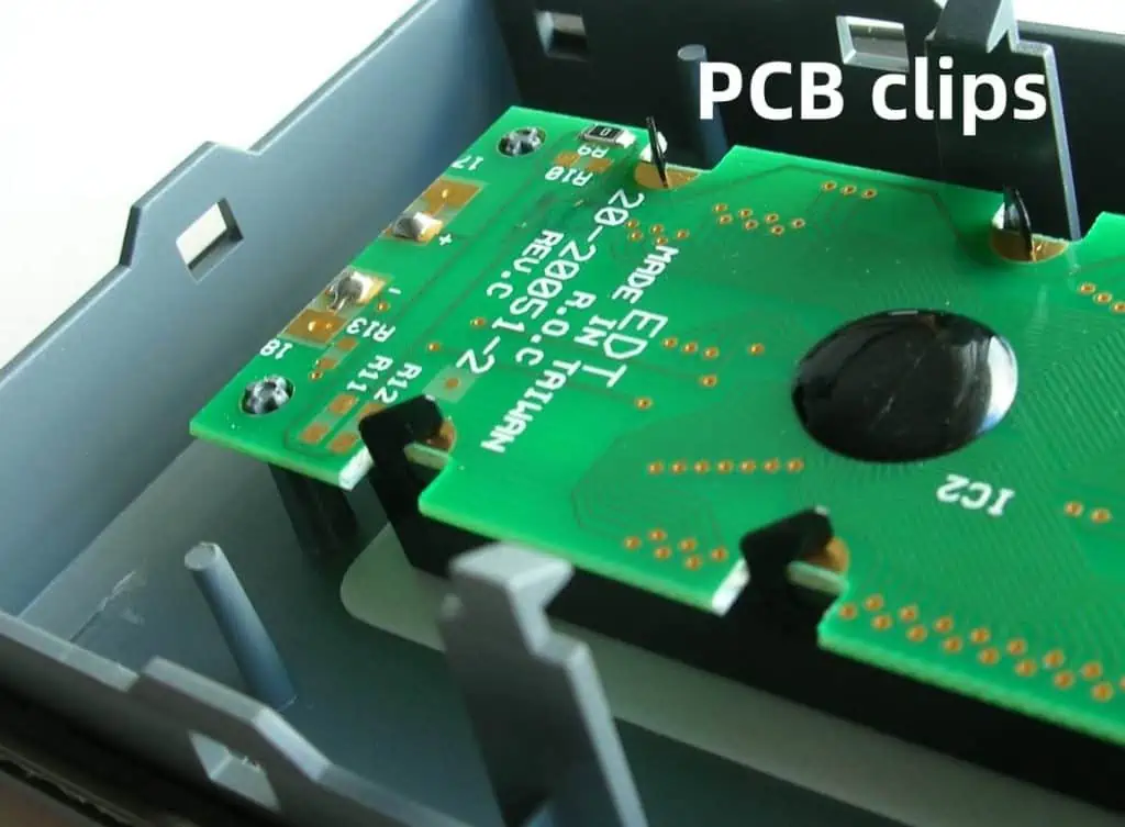
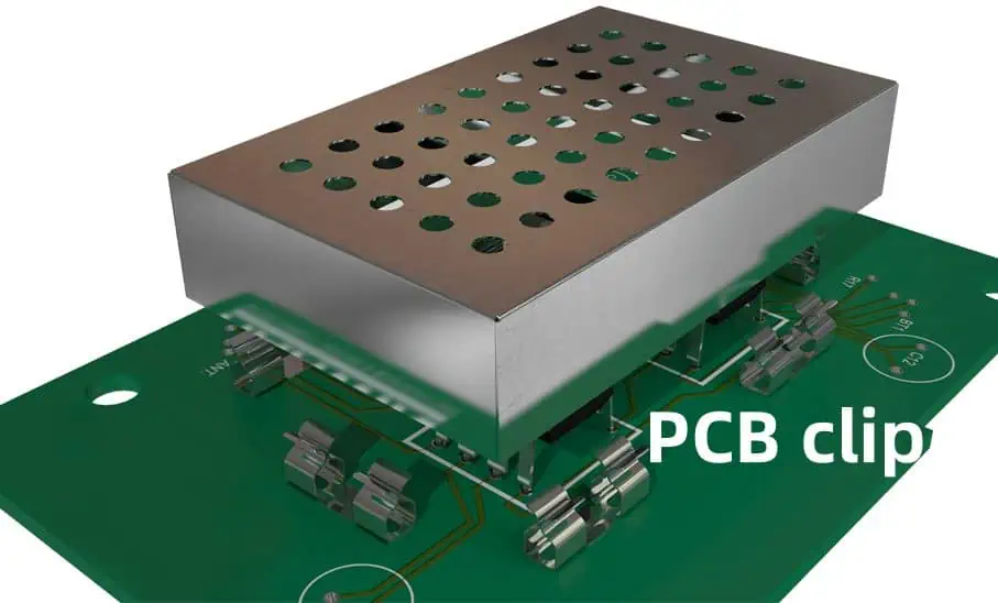
Plate Mounted Switches
Plate mounted switches are secured to a mounting plate which provides mechanical support and allows integration into an enclosure and panel design. The plate also enables labeling and provides alignment guides for assembly.
The plate is mounted separately from the PCB and provides the structure to hold the switches. Wires or connectors route signals between the switches and PCB.
Some typical types of plate mount switches:
Control Switches
- Illuminated pushbuttons
- Emergency stop switches
- Selector switches
- Toggle switches
Metal / Plastic Body Switches
- Industrial pushbuttons
- Heavy duty switches rated for high voltage/current
- Harsh environment sealed switches
Benefits of Plate Mounting
- Robustness – The plate provides mechanical support against vibration, shock, and continuous use.
- Switch access – Panel integration allows operator accessibility without constraints from PCB location.
- Large switch sizes – More robust switches can be used compared to only smaller PCB mount types.
- Custom labeling – The plate allows easy application of port designations, functions, warnings etc.
- Separate assembly – Switches and plate can be assembled independently from the PCB assembly.
- Easier replacement – Faulty switches can be changed without desoldering from PCB.
Drawbacks of Plate Mounting
- Increased cost – Additional plate and assembly operations required.
- Larger assembly – Greater overall volume required to accommodate plate.
- Wiring – Cables or connectors needed between plate and PCB.
- Design complexity – Plate integration must fit overall enclosure design.
- Difficult customization – Limited ability to modify switch position or size.
Applications of Plate Mounted Switches
Plate mounted switches are preferred for:
- Industrial machinery and control panels
- Instrumentation and test equipment
- Medical and scientific equipment
- Automotive dashboards and controls
- Aviation and marine controls
- Commercial equipment like vending machines
The external accessibility and custom labeling enabled by plate mounting suit these use cases.
Detailed Comparison of Mounting Methods

The following sections provide a more in-depth comparison between PCB mounted and plate mounted switches across various factors relevant to design and manufacturing.
Board Area Efficiency
- PCB Mount – Switch footprints consume space on the PCB that could be used for other components or routing. High density PCB mount switches are available with smaller footprint.
- Plate Mount – No PCB area is taken up since switches stand off from the board. However, the plate itself requires allocation of space.
Customization Options
- PCB Mount – Limited customization of switch position or appearance. However, PCB pads and silkscreen legends can be tailored.
- Plate Mount – Highly customizable including switch types, sizes, positions, labeling, colors, and board-to-plate standoffs.
Ease of Assembly
- PCB Mount – Switches placed and soldered during regular SMT and thru-hole assembly process along with other components. Minimal additional steps.
- Plate Mount – Requires additional assembly steps to populate the plate with switches and fasten the plate to the enclosure. More complex overall.
Manufacturing Cost
- PCB Mount – Lower cost since leverages existing PCB. May allow elimination of separate plates.
- Plate Mount – Additional cost for custom plate fabrication and assembly. However, may reduce PCB layers needed.
Reliability and Durability
- PCB Mount – Vulnerable to PCB flexing which can crack solder joints or pads after prolonged use.
- Plate Mount – Withstands high-stress applications with vibration or shock. Protects PCB from flex damage.
Ease of Switch Replacement
- PCB Mount – Requires de-soldering faulty switches and soldering new ones. Risk of pad damage.
- Plate Mount – Quick replacement by unfastening switch from plate. Much simpler with no soldering.
Available Switch Types and Sizes
- PCB Mount – Typically limited to smaller tactile, toggle, slide, snap-action, and DIP switches sized for PCB.
- Plate Mount – Supports wide range including sealed, 22mm, 30mm, 40mm, 60mm, and larger operator sizes.
Integration with Enclosures
- PCB Mount – Constrained by fixed PCB location; may make switch access difficult in enclosure.
- Plate Mount – Simplifies cutouts and access ports since plate location is adjustable.
Aesthetics
- PCB Mount – Harder to customize appearance beyond switch itself.
- Plate Mount – Allows additional labeling, colors, illumination, finishes for greater styling.
EMC and Grounding
- PCB Mount – Good continuity to PCB ground plane.
- Plate Mount – Requires attention to short grounding wires or clips.
Plate Mounting Switch Design Considerations
Designing successfully with plate mounted switches requires consideration of several factors:
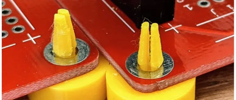
- Plate material – Stainless steel, aluminum and plastics like polycarbonate are common. Material must have adequate structural strength.
- Plate thickness – Thicker plates sustain rugged use but increase weight. 3mm is typical for metal plates.
- Mounting and positioning – Clear access for operators is key. Mounting points to enclosure must be robust.
- Switch spacing – Adequate spacing for gripping and operating the switch actuators. ~20mm typical minimum.
- Actuator sealing – Sealing boots may be needed in dusty/humid environments to block contamination. Potting can protect internally.
- Legends and labeling – Laser etching, engraving, screen printing are options. Urethane or acrylic overlays also used.
- Light pipes for indicators – Required to visually guide operators and annunciate switch states.
- Grounding – Important for ESD, EMI protection. Ground plate via mounting screws/eyelets.
- Wire strain relief – Clamps and ties necessary to secure wires/cables between plate and PCB.
Paying attention to these aspects ensures reliable, long-term operation of plate mounted switch assemblies in demanding conditions.
PCB Layout Guidelines for Switches

Some PCB design guidelines to follow for either PCB mounted switches or plate mount with PCB interfaces:
- Place switches near edge connectors for accessibility. Avoid burial under tall components.
- Group associated switches together in functional blocks for usability.
- Follow manufacturer recommended layout patterns for switch terminals and grounding pads.
- Use generous pad sizes for switch contacts to account for vibration.
- Include locator features like corner chamfers to aid placement.
- Provide clearance zones around switches for product assembly access.
- Enable sufficient routing keepout area around switches for traces, vias and shapes.
- Include test points to verify switch contact operation after assembly.
- Follow recommended ESD/EMI practices like grounding and filtering.
PCB design accommodations like these facilitate easy switch integration and reliable performance.
Comparison Summary
| Factor | PCB Mount | Plate Mount |
|---|---|---|
| Board area efficiency | Low – consumes PCB space | High – separate from PCB |
| Customization ability | Low – limited to pads/legends | High – switch types, labeling, colors |
| Assembly complexity | Simple – added to normal PCB assembly | Complex – additional plate population and mounting |
| Manufacturing cost | Lower – leverages existing PCB | Higher – extra plate and hardware |
| Reliability and durability | Lower – vulnerable to PCB flexing | Higher – plate provides robustness |
| Ease of switch replacement | Hard – requires de-soldering | Easy – just unfasten from plate |
| Available switch size and variety | Limited by PCB sizes | Wide selection possible |
| Enclosure integration | Constrained by PCB location | Flexible positioning |
| Aesthetics | Limited | Extensive labeling and styling options |
| Grounding | Direct via PCB plane | Needs wire clips or lugs |
In summary, plate mounted switches offer more flexibility and customization, while PCB mounts provide simpler assembly with lower costs. Consider tradeoffs like these when selecting between the two approaches for a given product.
Conclusion
- PCB mount switches solder directly to the PCB, minimizing assembly steps but consuming board space.
- Plate mount switches attach to a separate plate for mechanical support and panel integration.
- PCB mount suits low-cost consumer devices with space constraints.
- Plate mount accommodates heavy-duty switches in industrial equipment and machinery.
- Plate mounting aids switch accessibility and labeling in enclosure design.
- PCB switching layout requires attention to accessibility, grouping, and grounding.
- There are key tradeoffs between simplicity vs customization that guide mounting choice.
In summary, understand the differences in design, assembly, and capabilities between PCB and plate mounted switches. Analyze the requirements of the target application and weigh the pros and cons to select the best approach. Employ recommended design practices to successfully incorporate switches using either method.
Frequently Asked Questions
Q: What are some alternatives to PCB and plate mounting of switches?
Some other mounting approaches include:
- Panel mounted – Switches fasten directly to enclosure cutouts independent of PCB.
- Chassis mounted – Switches secured to metal chassis frame or structure of the product.
- Rack mounted – Switches designed for mounting onto standard 19″ equipment racks.
- DIN rail mounted – Switches clip onto standard DIN rails widely used in industrial settings.
Each method has advantages in certain applications similar to PCB vs plate mounting.
Q: How are plate mount switches interfaced to the PCB?
Common ways to connect plate mount switches to the PCB:
- Discrete wires soldered directly to PCB pads
- Insulated quick-disconnect terminals
- Ribbon cables with IDC headers
- Circular connector with screw terminals
The interface approach depends on switch type, ruggedness needed, and assembly process.
Q: What design factors affect switch reliability?
Reliability is impacted by:
- Switch contact material and rating – gold vs silver, AC/DC specs
- Enclosure seals against dust/moisture
- Impact of mechanical vibration/shocks
- Avoiding stress on solder joints or terminations
- Preventing switch contamination from environmental factors
Q: How are human factors considered in switch mounting designs?
Aspects like these need attention:
- Placing switches within easy reach envelopes
- Spacing for unimpeded grip and actuation
- Clear sightlines free of obstruction
- Intuitive grouping of related functions
- Distinctive labeling and visual indication
- Providing mechanical resistance and tactile feedback
Q: What safety precautions apply for exposed high voltage switches?
For hazardous voltages:
- Enclose switch fully with interlock shields
- Allow servicing only after voltage discharge
- Warning labels and color coding
- Special high voltage training
- Regulatory standards compliance (UL, IEC etc.)