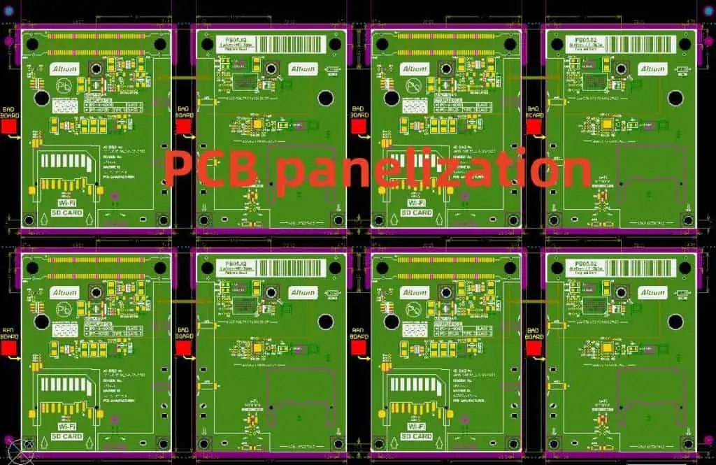
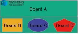
Panelization is the process of arranging multiple PCB designs onto larger panels for efficient board fabrication, assembly and testing. Panelizing maximizes board quantity per panel and minimizes material waste. Panelization is typically performed with specialized software tools that automate placement and routing of boards based on panel design rules.
This article provides recommendations on selecting suitable PCB panelization software and best practice guidelines for panel layouts to achieve optimal results.

Benefits of Panelization
The key benefits of panelizing PCB designs include:
- Reduced fabrication and assembly costs per board
- Improved material utilization with less waste
- Simultaneous processing of multiple boards
- Enabled automation with handling fixtures
- Simplified testing and calibration
- Faster assembly process flow
- Protection of finished boards in panels
- Support for materials like flex or rigid-flex
By panelizing properly with software, average costs can be decreased by up to 40% versus single board processing.
Panelization Software Evaluation Criteria

Consider the following when selecting PCB panelization software:
Input Format Support – Accepts major PCB design formats like ODB++, IPC-2581, DXF, Gerber.
Output File Generation – Produces panel drawings, drill and fabrication files, assembly data.
Design Rule Checks – Automatically validates panel clearances, tool access, placement.
Panel Optimization – Efficiently fits boards based on spacing rules and material sizes.
Board Rotation – Ability to rotate boards for optimal fit.
Step Panels – Allows creating stepped panels with overlap for panel breakpoints.
Fiducials and Tooling – Handles adding fiducials, rails, adhesives, labels.
Routed Tabs and Breakouts – Provides options for tab designs and tab routing between boards.
Multi-Vendor Support – Generates data in formats used by various fabricators, assemblers, testers.
Integration – Imports designs from CAD tools and integrates with CAM systems.
Automation – Scriptable to enable batch panelization across multiple designs.
Selecting software with robust panel design features ensures efficient panelization.
Panel Design Guidelines
Well-designed PCB panels optimize fabrication, assembly, testing and depaneling. Guidelines include:
Panel Size
- Select standard fabrication sizes like 18”x24”, 21”x24”, etc.
- Larger sizes enable more boards but impact handling.
- Consider final rigid panel thickness.
- Match panel size to processing equipment.
Board Population
- Pack boards tightly but allow minimum spacing rules.
- Typical spacing is 0.2” to 0.3” between boards.
- Ensure accessibility for probers, pick and place heads.
- Reduce placement scrap fall zones.
Board Orientation
- Orient boards optimally to maximize quantity.
- Rotate boards to align with panel edges.
- Consider number of unique orientations for simplicity.
Route Channels
- Add routing tabs/rails in channels between boards.
- Observe minimum tab width for rigidity during routing.
- Corner chamfer helps reduce tab remnants after routing.
Breakouts
- Use V-Score or mouse bites to form sections for breakout.
- Alternate tab locations between sections.
- Determine if breakouts are manual or routed.
Fiducials
- Add fiducials for assembly and test systems alignment.
- Use generous capture pads.
- Prevent fiducial shadowing by components.
Tooling Holes
- Add tooling holes for alignment pins on assembly/test systems.
- Tooling holes may require greater accuracy than fiducials.
Other Panel Features
- Include panel frame for handling.
- Add adhesives near center and edges to reinforce panels.
- Incorporate debug access points.
- Consider depaneling access holes for boards surrounded by others.
Panel Fabrication
- Specify tight registration between layers and processes.
- Require excellent drill location accuracy.
- Expect intensive incoming inspection procedures.
Following these guidelines yields reliable, high yielding panels.
Panelization Software Tools

Here are some recommended panelization software tools:
Altium Panelizer – Allows panel planning with automated optimal placements. Includes design rule checking and output generation.
Mentor Valor Panelization – Supports panel design, documentation, fabrication and assembly data. Integrates with Xpedition PCB tools.
Zuken CR-8000 Panelization – Performs multi-board panel layout with extensive rule checks. Links to CAD and CAM tools.
DownStream BluePrint Panelizer – Drag-and-drop panel creation. Links to CAM for phototools and NC drill generation.
Ucamco Integr8tor – Combines incoming netlists then auto-panels design with automation capabilities.
PADS Panelizer – Places boards interactively with defined spacing constraints to generate panels.
InPanel – Auto-populates panels using defined rules. Checking routines validate panel designs.
There are also panelization capabilities offered by major PCB vendors to prepare customer designs for volume fabrication.
Panel Waste Optimization
Careful panel planning minimizes material waste. Some optimization guidelines:
- Assess typical board area versus target panel sizes.
- Determine typical quantities needing production.
- Select panel sizes to minimize unused areas.
- Analyze blank areas to quantify waste costs.
- Group similar sized boards on common panels when possible.
- Prioritize high volume boards on optimized panels.
- Compare alternate orientations and rotations to find most efficient layout.
- Adjust spacing rules to fit more boards per panel if reworkable.
- Request panel fabrication quotes with expected utilization percentages.
- Determine cost tradeoffs increasing panel sizes for more boards vs. material costs.
- Review panel designs regularly as boards change to maximize usage.
Spending time optimizing panel efficiency delivers significant cost reductions.
Handling Small Boards

Panelizing can also support easier handling of small boards:
- Group multiple small boards together on panels for stability.
- Surround each small board with generous routing channels.
- Provide open access points in the panel for probing.
- Define panel sections for breaking out board groupings.
- Add adhesives between boards to keep together before depaneling.
- Design panels so boards can depanel individually without disturbing neighbors.
- Include alignment fiducials near each localized board region.
With care, panelization allows cost-effective volume production of small boards.
Panel Design Rule Checks
Panelization software should perform design rule checks including:
- Minimum clearance between boards.
- Minimum tab width for rigidity.
- Tab positioning on alternating sides.
- Sufficient fiducial landing area.
- Access spacing for assembly nozzles/probes.
- Allowed panel overhang for board outlines.
- Annular ring clearance around tooling holes.
- Elimination of vacant pad or trace exposure whenever possible.
- Validation of minimum web thickness for scoring residuals.
Automated checking prevents defects and ensures a panel is fabricatable.
Panel Fabrication and Assembly Notes
Critical notes to detail on panel drawings:
- Layer registration tolerance.
- Etch compensation requirements.
- Pad geometry and soldermask tolerances.
- Allowable stretch or shrink during lamination.
- Permitted handling grabs/flange regions.
- Drilling entrance/exit constraints for burrs.
- Surface finish control on live tooling hole areas.
- Pad geometry protection near tabs and rails.
- Expectations for untouched fiducial and tooling hole accuracy.
- Breakout force limitations to prevent damage.
- Storage and handling requirements before assembly.
Clear specifications are vital for panel integrity during large volume fabrication.
Summary
- Panelization software maximizes material utilization, lowers average costs, and enables automation.
- Select software with excellent optimization, design rules checks, and output generation capabilities.
- Carefully design panels following spacing, tooling, breakout, and waste minimization guidelines.
- Validation checks performed by software prevent defects and ensure panel integrity.
- Panel-level engineering documentation highlights fabrication and assembly requirements at scale.
Panelizing with capable software combined with robust panel design guidelines ensures reliable volume PCB production with minimal waste.
Frequently Asked Questions

What are some key panel design rules manufacturers should follow?
Critical rules are minimum spacing between boards, tab routing widths, alternating tab locations, tooling hole annular rings, placement of fiducials, and clearance for assembly machine access. Setting and following these rules results in reliable panels.
How can PCB panelization reduce manufacturing costs?
By maximizing board quantity per panel, processing costs are amortized across more boards. Handling automation is enabled. Material waste is also reduced lowering raw material costs. Testing time per board decreases. Total savings average around 40% versus non-paneled boards.
What considerations are important for panel depaneling?
For depaneling, allow open access regions between boards, use generous router channels with chamfers, allow individual board removal without disturbing others, incorporate breakout subpanels, and indicate deburring requirements.
What panel thickness should be used?
Final panel thickness depends on board thickness and material. Aluminum entry and exit material can increase rigid panel thickness another 0.062”. Panels above 0.1” thickness may require handling adjustments.
How many different board orientations on one panel is optimal?
It is best to limit panel designs to no more than two unique board orientations when possible. More orientations increases assembly programming complexity and likelihood of misloaded boards. Well-designed panels can achieve high utilization with just one or two orientations.
