
RAYPCB · ENGINEERING REFERENCE
PCB EMI/EMC Design: Layout Checks Before Compliance Testing
Trace a disturbance from its source through its coupling path to the susceptible circuit or cable. Prepare layout changes and a reproducible pre-compliance test plan.
Original engineering guidance · References checked September 29, 2026
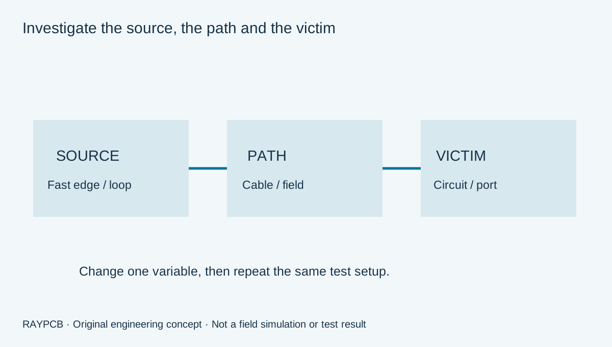
EMI/EMC layout review begins with a physical coupling mechanism
PCB EMI/EMC design aims to control unwanted disturbances and preserve intended operation in the product's electromagnetic environment. The board is one part of that product: cables, enclosure, power source, firmware, loads and operating modes can all affect the result. A layout checklist helps organize review, but it cannot certify emissions or immunity performance.
The most useful starting record has three parts: the disturbance source, the coupling path and the affected circuit or port. A fast digital edge, a switching power loop and an external transient are different sources. A trace pair, shared reference, cable and enclosure aperture are different paths. A symptom becomes actionable when those parts are connected to a reproducible observation.
This page is an electromagnetic-compatibility design guide. It is not a material-brand page, a certificate offer or a substitute for the applicable product standards. Use the PCB design workflow for the complete release process, and the ground-plane guide for detailed reference-path questions.
Separate design review, pre-compliance work and formal assessment
| Activity | Useful output | Limit of the evidence |
|---|---|---|
| Layout review | Annotated source, path and boundary observations | A drawing review does not measure emissions |
| Diagnostic measurement | Reproducible evidence about a suspected mechanism | A local probe result is not a complete product test |
| Pre-compliance comparison | Revision-to-revision result under a documented setup | A screening setup may differ from the required formal method |
| Formal product assessment | Report under the selected standard and configuration | Coverage is limited to the tested scope and conditions |
Before selecting a test, define the product, intended environment, ports and operating modes with the responsible compliance team. Requirements can differ for products that use similar circuit boards. This guide does not supply a universal emissions limit, immunity level or safety spacing. Record the applicable document editions and assessment decisions in the project rather than borrowing them from an unrelated example.
A test result without its configuration is difficult to use. Keep cable types and lengths, supply arrangement, enclosure state, loads, firmware and exercised functions with the record. If a noisy mode is only active briefly, explain how the test exercises it. If a modification changes the software activity, that change belongs in the comparison as much as a copper edit does.
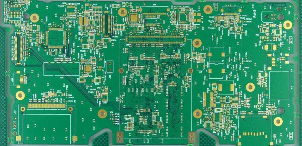
Identify current loops and switching events
For a digital circuit, the repetition frequency does not fully describe the edge spectrum. Driver transition behavior and loading matter. For a power converter, identify the loops whose current changes rapidly during switching and the nodes whose voltage changes rapidly. Keep the review anchored to the actual topology and the semiconductor manufacturer's layout guidance.
An illustrative investigation might find a disturbance that appears during a converter load step. Record whether the observation follows the load event, the switching frequency, a control transition or another synchronized function. Compare controlled operating modes before changing the layout. A correlation guides the next experiment but is not proof of a unique coupling mechanism.
Changing drive strength, slew rate or switching behavior can reduce one disturbance while affecting timing, efficiency or stability. Such adjustments should remain within device and system requirements. Avoid recommending a slower edge or spread-spectrum option as an unconditional improvement. The right design preserves the required function while addressing the identified interference path.
Review the return connection as carefully as the outgoing trace
The intended current loop includes a return path. A trace may be short while its return takes a long or poorly controlled route around an opening. Decoupling connections have geometry too; a capacitor value alone does not define the impedance seen at the device. Review placement, vias and reference conductors together at the relevant circuit boundary.
Reference-net changes deserve explicit attention. A signal moving between layers can introduce a return-transfer problem even when its copper length decreases. A mounting or connector modification can also change how current reaches the enclosure or power source. The layer map and mechanical assembly should be available during the EMI review, not kept in separate documents that nobody compares.
For adjacent-signal interference, use the focused PCB crosstalk guide. For a complete layout route, use the high-speed constraint guide. Those tasks help isolate a board-level mechanism before attributing every unwanted waveform to radiation from the whole product.
Treat the connector region as an electrical boundary
A cable can carry intended differential or single-ended signals while also providing an unintended common-mode path. Review connector pin assignments, reference connections, shield treatment and the relationship to chassis. A clean waveform on a local trace does not establish that current on the cable or enclosure is controlled.
Protection and filter components must be considered with their physical connections. A long route to a protective element can expose additional board area before the disturbance reaches it. A filter bypassed by adjacent coupling may not provide the behavior suggested by an isolated component specification. Follow the applicable protection-device data and validate the implemented path.
Do not connect all named grounds simply to make this region look continuous. Functional reference, chassis and protective earth have distinct roles, and isolation barriers must remain intentional. Any network across an isolation boundary requires the appropriate system and safety review. The interactive worksheet identifies that the boundary must be documented; it does not approve a connection.
Give noisy and sensitive functions a deliberate relationship
Functional partitioning should organize current paths and routing access. Place sensitive interfaces so their signal and reference connections do not unnecessarily share the switching region of a power stage. Keep the relevant analog reference close to its task. Plan the physical route between a connector and its protection or conditioning circuitry before filling the remaining board space.
Shielding is also a system design decision. A shield's connections, apertures and mechanical interfaces affect what it does. Adding a metal cover late in the project can change coupling or thermal conditions and may leave cable-related paths untouched. Document which mechanism the shield is intended to address and what evidence will evaluate it.
For an illustrative revision, move a connector filter to the intended boundary while keeping its component values unchanged. Compare the old and new arrangement under the same operating and measurement conditions. If the result improves, retain the exact geometry and setup in the record. Do not generalize the result into a universal placement distance for other connectors or bandwidths.
Build a source–path–victim investigation brief
Choose a disturbance category and coupling route, then describe the victim or observed symptom. Record whether the source loop, boundary and test configuration are documented. The worksheet generates a focused review brief with unresolved items, rather than a generic percentage score that might imply compliance.
RAYPCB ENGINEERING
High Speed RoutingEMI source–path–victim review brief
Loading EMI source–path–victim review brief…
The brief is a planning aid. It does not read schematics, calculate emissions, interpret a standards report or verify the fields marked documented. Download it and attach it manually with the relevant board region, system diagram and test record. No information is automatically sent to a manufacturer or analytics service by this tool.
Make each experiment explain something
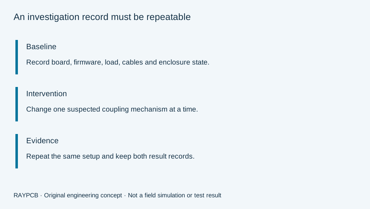
Start with a repeatable baseline. Record the symptom, operating mode and instrument settings, then form a hypothesis that links a source to a path and victim. Choose a modification that tests that relationship. Retain the original result and the modified result rather than only saving the better screenshot.
Several changes at once may be necessary to recover a schedule, but they limit what can be concluded about causality. State that limitation. A prototype modification made with temporary wires or shielding must also be translated into a producible and reviewed design. The released board and assembly should reproduce the intended electrical relationship rather than merely resemble the improvised fix.
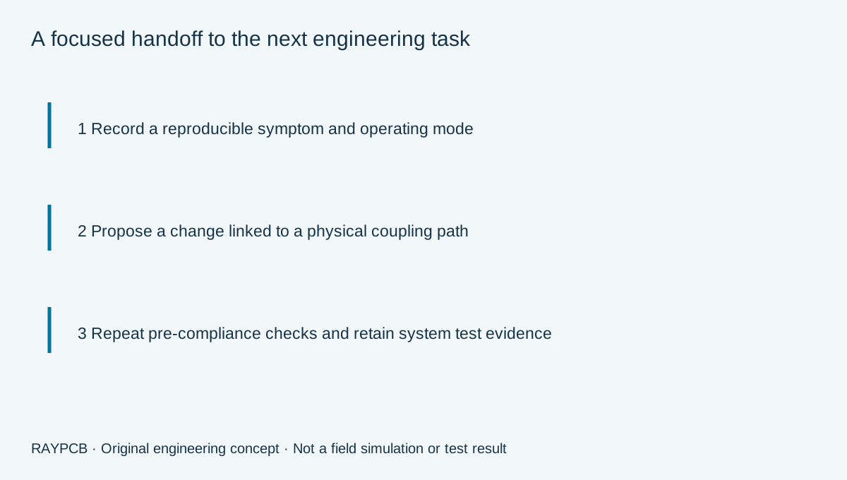
After a change, repeat relevant functional checks. A filter that reduces an observed disturbance may degrade an interface waveform; a reference connection may alter another port; a layout adjustment may affect thermal operation. The task is to achieve the complete product requirements, not maximize one diagnostic measurement in isolation.
Include assembly and mechanical configuration in the handoff
The handoff should identify the board revision, approved component population, firmware used for evaluation and mechanical details that affect the electrical boundary. Shield contacts, connector shells, mounting hardware and cable assemblies should not be left as untracked production choices when they influence the test configuration.
Define change-control triggers. A substitute filter, a different connector, a revised cable or an altered enclosure seam may need another review even when the PCB artwork is unchanged. Manufacturing records can preserve what was built, while the design owner determines what verification the change requires. Send unresolved requirements early when discussing fabrication or PCB assembly scope.
Questions about layout and EMC confidence
Does a multilayer board automatically pass EMC tests?
No. Additional layers can make a useful reference arrangement possible, but the implementation and complete product configuration still determine behavior. Layer count is not an emissions or immunity certificate.
Can a ferrite bead solve every noise problem?
No. Its behavior depends on frequency, bias, impedance environment and physical placement. Identify the current path and follow the component and circuit requirements. Adding an unspecified part can change the problem without resolving its cause.
Is a near-field scan a formal compliance test?
It can be a valuable diagnostic tool for locating or comparing active regions. Its scope differs from the prescribed setup of a complete product assessment. Preserve both types of evidence with clear labels rather than substituting one for the other.
What should an early engineering inquiry include?
Provide the relevant board region, system boundary, operating mode and observed symptom, plus available test conditions. Identify what is unknown. A focused question can be reviewed before a complete formal report exists, but the response should remain within the evidence available.
Further reading from primary technical sources
TI PCB Design Guidelines for Reduced EMI provides layout-oriented engineering background. TI high-speed interface guidance covers interface boundary considerations, and Analog Devices MT-031 provides grounding context. These engineering references do not select the complete product's legal or certification obligations.
Review the route with the actual stackup
Send the board revision, construction, quantity and the routing or signal-integrity question you need reviewed. Identify unresolved requirements so the response can address them.
Send requirements for reviewOptional: attach the downloaded worksheet manually. This guidance does not certify a design, approve a shipment or replace the applicable authorized standards.