How To Repair Damaged /Missing PCB Pads ?

How To Repair Damaged /Missing PCB Pads

Introduction

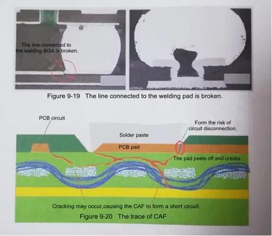
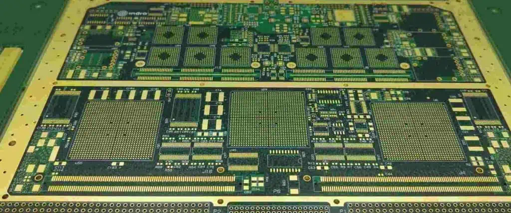
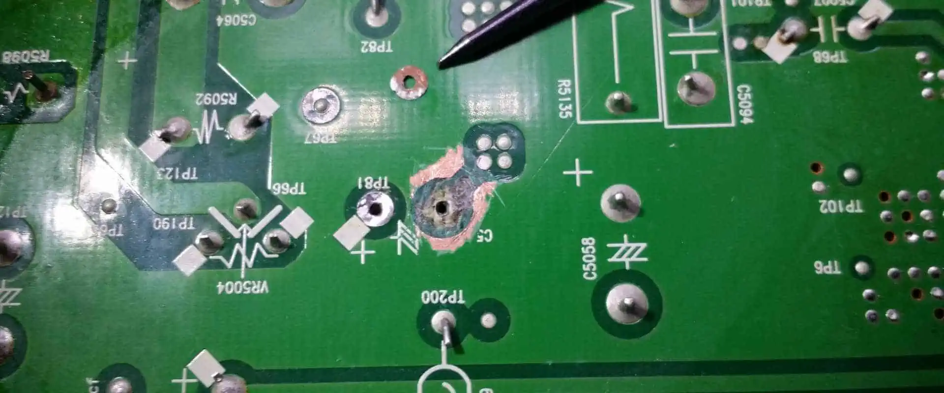
Printed circuit boards (PCBs) are susceptible to pad damage either during manufacturing or rework. Pads can become damaged or lifted off entirely from the board. This can render a PCB unusable since components cannot be soldered down properly. Fortunately, there are techniques available to repair missing or damaged pads and restore a PCB.

Pad repairs allow fixing defects rather than scrapping an entire PCB. However, all pad repairs should be approached carefully as they can affect long-term reliability if not done properly. This article provides repair methods for various pad damage scenarios.

Common Causes of Pad Damage

Some of the typical causes of pad damage include:

  • Excessive heat – Too much heat during soldering or desoldering can lift pads or cause the copper to de-laminate.
  • Mechanical damage – Scratches, cracks, indentations from tools can damage bond between pad and fiberglass.
  • Manufacturing defects – Etching issues, handling damage or drill misalignment may impair pads.
  • Corrosion – Environmental exposure leading to oxidation and corrosion under pads over time.
  • Handling damage – Stresses from flexing PCBs, shock or vibration can crack pads.
  • Multiple reworks – Repeated rework on a pad can wear it out and cause pad lift off.

Careful process control is key to avoid pad damage during assembly. But when pad damage does occur, selecting the optimal repair method is important.

Repair Considerations

How to repair Lifted Pad on PCB

Some key factors to evaluate when planning pad repairs:

  • Type and extent of damage – Missing pad, partially lifted pad, pad with crack or indentation, etc.
  • Location – Is damaged pad on outer or inner layer? Is it reachable for repair?
  • Pad purpose – Is it for through-hole or surface mount component? High speed or high power?
  • Layer type – Can ground or power plane layers be repaired, or only signal layers?
  • Available repair area – Is there sufficient space around damaged pad for repair?
  • Component re-attachment – Will repaired pad allow reliable solder joint for component re-attachment?
  • Costs – Does chosen repair method require additional tools, materials, or testing?
  • Reliability – Will repair withstand mechanical and thermal stresses during product lifetime?
  • Rework processes – Compatibility with available PCB assembly and test capabilities.

Evaluating these parameters will guide selection of the optimal repair approach.

Pad Repair Methods

Here are some common methods used for repairing damaged or missing pads on PCBs:

1. Copper Foil Patch

  • Apply small copper foil square over damaged pad area. Secure with epoxy.
  • Suitable for outer layer pad repairs where foil patch is accessible.
  • Low cost, simple method. Reliability limited by epoxy strength.
  • Works for surface mount or through-hole pad repairs.

2. Copper Tape Patch

  • Use conductive copper tape over damaged pad site. Cover with non-conductive Kapton tape.
  • Wider tape increases reliability compared to foil. Foil may lift off during rework.
  • Easy outer layer repair method. Capable of repairing elongaged pads.
  • Limitations based on space needed for tape adhesion.

3. Circuit Frame

  • Glue insulating frame around damaged pad, then fill with conductive epoxy.
  • Provides containment for epoxy repair material.
  • Allows repair of any pad size. Handles voids under pads.
  • Requires significant space around damaged pad.

4. Conformal Coating

  • Use insulating acrylic coating over damaged pad area.
  • Coat entire PCB area under component to insulate. Then apply conductive coating to rebuild pad.
  • Allows repair when limited space around pad.
  • Conformal coatings prone to thermal damage during rework.

5. Solder Mask Bridge

  • Use solder mask to bridge the gap between disconnected pad segments.
  • For partial pad lifts. Mask reconstitutes pad electrically.
  • Requires access to solder mask artwork and selective imaging capability.
  • Provides reliable repair. Maintains original pad geometry.

6. Epoxy Fill

  • Inject conductive epoxy under the pad to re-adhere it. May also inject epoxy under component leads.
  • Allows repair without modifying pad geometry.
  • Significant process expertise needed for reliable injection. Risk of shorting under pad.
  • Repaired pad prone to re-lifting if epoxy not fully cured.

7. Trace Bridge Jumper

  • Solder thin insulated wire between disconnected pad segments.
  • Simple method to bridge small pad gaps.
  • Limited space required provided wire routing space exists.
  • Wire flexing can compromise long term reliability.

8. PC Board Rework

  • For multilayer boards, strip off layers to expose inner pad, repair pad, then rebuild board.
  • Allows access to inner layers not repairable otherwise.
  • Highly complex. Only for very expensive PCBs where re-manufacture not possible.
  • Skilled technicians and specialized tools needed.

The optimal repair technique depends on the pad type, layer location, reliability requirements, and available tools.

Process Steps for Pad Repairs

Here is an overview of the typical process sequence to execute a pad repair:

  1. Visually inspect pad damage under microscope. Check for cracks, lifting, or missing copper.
  2. Remove any residual solder or component debris from pad area with solder wick and flux.
  3. Select repair method based on pad characteristics and constraints. Gather required materials and tools.
  4. Prepare pad area – remove oxide with abrasive pad, clean pad thoroughly.
  5. Execute pad repair procedure using selected method.
  6. For multilayer boards, use ohmmeter to confirm electrical connectivity after repair.
  7. Apply flux to repaired pad area. Solder component lead or ball to pad using soldering iron.
  8. Clean repaired area. Inspect joint integrity using microscope.
  9. Perform electrical testing and any re-programming of board.
  10. Conduct X-ray inspection of repaired solder joints if required.
  11. Qualify reliability with temperature cycling, vibration, mechanical shock testing.

With careful process control, damaged PCB pads can be repaired successfully. But appropriate materials, operator skill levels, and inspection steps are vital to ensure robust, reliable repairs.

Guidelines for Reliable Pad Repairs

Follow these guidelines when repairing damaged pads to improve repair success and long-term reliability:

  • Select the optimal repair method based on damage type, pad characteristics, and PCB design constraints.
  • Remove all solder and oxides from pad area before attempting repair. Scrub with abrasives if needed.
  • Ensure repair materials are compatible with PCB and components. Conduct material testing if unknown.
  • Follow manufacturer instructions for surface prep, application procedures, cure times, etc.
  • Repair area should exceed damaged area by at least 2X for reliable adhesion.
  • Visually inspect for cracks, uneven surface, or voids after repair before rework.
  • Soldering profiles may need adjustment to avoid re-lifting repaired pad during attachment.
  • X-ray inspection of solder joints validates proper lead/pad interface.
  • Conduct environmental stress testing at temperature and load extremes expected in application.
  • Monitor initial field failures to identify any long-term reliability trends.

With careful process control and testing, PCB pads damaged during fabrication or assembly can be restored successfully.

Summary

  • Pad damage on PCBs can occur due to manufacturing issues or operational stresses. This can impair board function.
  • Assessing the pad characteristics and constraints guides optimal repair method selection.
  • Common repair techniques include copper foil or tape patching, epoxy injection, solder mask bridging, jumper wires, and full PCB rework.
  • Process steps encompass pad cleaning, material preparation, repair execution, soldering, inspection, and qualification testing.
  • Following repair guidelines will improve reliability. But evaluation under operational loads is key to validating pad repair integrity.

FAQ

What is the easiest PCB pad repair method?

The simplest repair methods are copper foil or copper tape patching. These allow quick repairs of outer layer pads, require minimal tools, and have low material costs. However, long-term reliability may be limited.

Can conformal coating be used to repair PCB pads?

Yes, a conformal coating can be applied over the damaged pad area to insulate, then a conductive coating added to rebuild the pad. This technique provides reliable repairs when space around the pad is very constrained.

Is it possible to repair inner layer PCB pads?

Yes, options like epoxy injection or full PCB rework allow access and repair of inner layer pads. But these approaches require significant expertise and are far more complex than outer layer repairs.

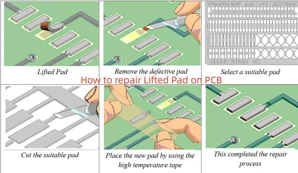
How do you repair a lifted PCB pad?

For partially lifted pads, epoxy injection to re-adhere the pad is an option. Solder mask bridging can also reconnect segmented pads. Completely missing pads need to be rebuilt using conformal coating or frame + epoxy methods.

Can jumper wires be used to repair PCB pads?

For small pad gaps or tears, soldering thin insulated jumper wires can bridge across and reconnect the damaged pad segments. This provides a simple way to repair pads when trace routing space permits bridging.

What is Difference Between Single-sided and Double-sided SMT Assembly

dip assembly
YouTube video

1. Single-sided SMT Process:

Incoming Inspection => Screen Solder Paste Printing(Dispense surface mount adhesives) => Surface Mounting => Drying(Solidifying) => Reflow Soldering => Clean out => VI&AOI => Rework/Repair.

Introduction About Single-sided SMT Assembly

2. Double-sided SMT Process:

A. Incoming Inspection => Screen Solder Paste Printing on PCB A side (Dispense surface mount adhesives) => Screen Solder Paste Printing on PCB B side (Dispense surface mount adhesives) => Surface Mounting => Drying(Solidifying) => Reflow Soldering(Better on B side) => Clean out => VI&AOI => Rework/Repair.

B. Incoming Inspection => Screen Solder Paste Printing on PCB A side (Dispense surface mount adhesives) =>Surface Mounting => Drying (Solidifying) => Reflow Soldering on A side => Clean out => Plate Turnover => Dispense surface mount adhesives on PCB B side => Surface Mounting => Solidifying => Wave Soldering on B side => Clean out => VI&AOI => Rework/Repair.

This process is suitable for reflow soldering on the A side of the PCB and Wave Soldering on the B side. Only the pins less than the SOT or SOIC (28) in the SMD of PCB B side , then can use this process.

3. Single-sided mixed pcb assembly Process:

Incoming Inspection => Screen Solder Paste Printing on PCB A side (Dispense surface mount adhesives) => Surface Mounting => Drying(Solidifying) => Reflow Soldering => Clean out => DIP => Wave Soldering => Clean out => VI&AOI => Rework/Repair.

4. Double-sidedmixed Process:

A. Incoming Inspection =>Dispense surface mount adhesives on PCB B side => Surface Mounting => Solidifying => Plate Turnover => DIP on PCB A side => Wave Soldering => Clean out => VI&AOI => Rework/Repair.

First SMT, then DIP, suitable for SMD components more than separating components.

B. Incoming Inspection=> DIP on PCB A side(Bending Pin) => Plate Turnover => Dispense surface mount adhesives on PCB B side => Surface Mounting => Solidifying => Plate Turnover => Wave Soldering => Clean out => VI&AOI => Rework/Repair.

First DIP, then SMT, suitable for separating components more than SMD components .

double sided pcb assembly process

C. Incoming Inspection=> Screen Solder Paste Printing on PCB A side => Surface Mounting => Drying => Reflow Soldering => DIP (Bending Pins) => Plate Turnover => Dispense surface mount adhesives on PCB B side => Surface Mounting => Solidifying => Plate Turnover => Wave Soldering => Clean out => VI&AOI => Rework/Repair A side mixed, B side mounted.

D. Incoming Inspection=> Screen Solder Paste Printing on PCB B side => Surface Mounting => Solidifying => Plate Turnover => Screen Solder Paste Printing on PCB A side => Surface Mounting => Reflow Soldering on PCB A side => DIP => Wave Soldering on B side => Clean out => VI&AOI => Rework/Repair A side mixed, B side mounted.

First SMD on two side, Reflow Soldering, then DIP, Wave Soldering.

E. Incoming Inspection=> Screen Solder Paste Printing on PCB B side(Dispense surface mount adhesives) => Surface Mounting => Drying(Solidifying) => Reflow Soldering => Plate Turnover => Screen Solder Paste Printing on PCB A side => Surface Mounting => Drying => Reflow Soldering(It could be Partial welding) => DIP => Wave Soldering 2(If there are few components, you can use manual welding) => Clean out => VI&AOI => Rework/Repair A side mounted, B side mixed.

 5. Double-sided prototype PCB Assembly Process 

A. Incoming Inspection=> Screen Solder Paste Printing on PCB A side (Dispense surface mount adhesives => Surface Mounting => Drying(Solidifying) => Reflow Soldering on A side => Clean out => Plate Turnover => Screen Solder Paste Printing on PCB B side(Dispense surface mount adhesives) => Surface Mounting => Drying => Reflow Soldering(Better on B side) => Clean out => VI&AOI => Rework/Repair.

This process is suitable for mounting large SMDs on both sides of the PCB such as PLCC.

pcb assembly flow process

B. Incoming Inspection=> Screen Solder Paste Printing on PCB A side(Dispense surface mount adhesives => Surface Mounting => Drying(Solidifying) => Reflow Soldering on A side => Clean out => Plate Turnover => Screen Solder Paste Printing on PCB B side(Dispense surface mount adhesives) => Surface Mounting => Solidifying => Wave Soldering on B side => Clean out => VI&AOI => Rework/Repair.

This process is suitable for reflow on the A side of the PCB.

How to Design a PCB Layout

ATmega328P PCB Layout

Introduction

Printed circuit board (PCB) layout design is a complex engineering art involving the layout of components and interconnections on a PCB to realize the circuit schematic functionality. A good PCB layout ensures proper signal and power integrity, electromagnetic compatibility, thermal management, manufacturability, and reliability of the product. This article provides a step-by-step guide on designing effective PCB layouts.

PCB Layout Design Steps

The major steps involved in designing the layout for a PCB are:

  1. Planning the layout and creating a stackup
  2. Placing components strategically
  3. Routing traces taking signal integrity into account
  4. Adding power/ground planes and ensuring decoupling
  5. Incorporating thermal management features
  6. Adding mounting holes, connectors, indicators, etc.
  7. Finalizing layer stacks and interfaces
  8. Checking design rule and manufacturing compliance
  9. Validating with DFx analysis like signal, power, thermal, EMI
  10. Iterating to optimize based on analysis feedback

Proper planning is key before starting the actual layout to avoid sub-optimal results requiring rework.

1. Layout Planning and Stackup Design

Hardware Layout
Hardware Layout

The first step is planning the layout architecture and defining the PCB layer stackup.

Key planning activities:

  • Understand PCBspecs – board dimensions, layer count, density, etc.
  • Review schematic for component types and counts
  • Plan partitioning for analog and digital sections
  • Define interfaces, high speed routing needs
  • Plan power architecture and decoupling strategy
  • Identify high power components needing cooling
  • Understand enclosure and assembly constraints
  • List critical nets needing impedance control
  • Gather applicable routing guidelines from IPC and OEMs

Defining layer stackup:

  • Select number of layers suitable for density
  • Choose dielectric materials based on performance
  • Determine copper weights for current needs
  • Add impedance control layers if needed
  • Assign plane layers (power, ground)
  • Plan signal routing layers
  • Consider double-sided component placement
  • Incorporate internal thermal vias/layers if necessary
  • Specify thickness, finish and solder mask for outer layers

Careful planning and stackup design ensures effective layout of all sub-systems.

2. Component Placement

Next step is intelligently placing components on the board.

Placement guidelines:

  • Group associated circuits together
  • Ensure important nets have short paths
  • High speed ICs close to connectors
  • Match component footprint to placement side
  • Distribute heat sources avoiding hotspots
  • Allow access to testpoints
  • Ensure components fit within board outline
  • Maintain clearance between components
  • Standardize orientation for polarized parts
  • Consider rework access requirements
  • Define placement zones for partitioned layout

Good component placement minimizes interconnect lengths, noise coupling, and thermal issues while taking assembly needs into account.

3. Signal Trace Routing

PCB Antenna Layout
PCB Antenna Layout

With components placed, signal interconnects between pins are routed:

Signal trace routing tips:

  • Use appropriate trace widths based on current
  • Minimize length for critical signals like clocks
  • Avoid 90ยฐ angles. Use 45ยฐ bends.
  • Route noise-sensitive signals away from aggressors
  • Provide isolation channels between digital and analog
  • Use impedance matching techniques if needed
  • Take care of high speed interfaces
  • Facilitate test probe accessibility
  • Enable visual inspection where needed
  • Allow space between traces for manufacturing

Intelligent trace routing controls impedance, EMI and signal quality while enabling testability.

4. Power Distribution and Decoupling

Proper PCB power distribution is key for stable functioning of circuits.

Power distribution considerations:

  • Use power/ground planes to distribute current
  • Decide on split or contiguous planes
  • Stack-up should sandwich signal layers between power layers
  • Use wide traces/polygons for power connections
  • Add local vias in pads to connect devices to power plane
  • Include thick interconnects between layers

Decoupling guidelines:

  • Place bypass caps close to ICs on same layer
  • Minimize trace length between cap and pin
  • Select suitable capacitors for HF and LF decoupling
  • Add sufficient bulk capacitance distributed around the board

Together, a robust power distribution network and decoupling strategy provide clean stable supply voltages to all devices.

5. Thermal Management

Proper cooling provisions must be incorporated for heat generating components:

Thermal design techniques:

  • Identify components needing heatsinks from power dissipation
  • Position hot parts for maximum heat sink contact
  • Ensure air flow access over heat sinks and vents
  • Use thermal vias under hot device pads
  • Add internal thermal layers connected by vias
  • Incorporate thick copper planes for spreading heat
  • Define thermal pads for device cooling
  • Check for hot spots and temperature gradients

This removes heat efficiently from critical high power devices.

6. Mechanical Features

PCB layoutย lineย design

Additional mechanical elements are added:

  • Mounting holes with correct diameter and annular ring spacing
  • Edge connectors, testpoints, indicators and switches
  • Brackets, clamps and strengtheners if needed
  • Mark component IDs, polarity, ratings as needed
  • Add board outline with proper corner chamfers
  • Include any required assembly instructions

These features facilitate mounting, assembly and usage of the designed PCB.

7. Finalizing Layer Stack

With routing completed, the individual layers are finalized:

  • Review all routing on layers, rearrange if needed
  • Check for manufacturing spacing violations
  • Verify alignment between layers for vias
  • Add reference markers for layer alignments
  • Insert testpoints for probing individual layers
  • Check plane void areas affecting current flow
  • Define minimum annular rings for vias
  • Confirm margins from edge meet requirements

This completes the detailed inner layer builds ready for integration.

8. Design Rule Checks

The PCB layout is then validated against:

  • Electrical rules: spacing between traces, pads, and planes based on voltage levels and insulation needs
  • Routing rules: trace widths and clearances, via dimensions, acute angle avoidance
  • Manufacturing rules: capabilities of PCB fabrication process like minimum track width, hole size, spacing

Tools like designersRule inside Cadence Allegro can automate checking against IPC and OEM guidelines. Errors must be fixed to ensure manufacturability.

9. DFx Analysis

The next step is verifying the design using DFx simulations:

  • Signal integrity: Check for reflections, crosstalk, timing issues using IBIS models
  • Power integrity: Simulate power distribution network stability and resonance
  • Thermal: Verify temperature profiles using tools like IcePak
  • EMI/EMC: Model radiated and conducted emissions
  • Mechanical: Stress analysis, vibration and shock checks

This validates the design meets all functional requirements before release.

10. Layout Optimization

Corne PCB Layout
Corne PCB Layout

Based on the analysis feedback, layout issues are addressed:

  • Tune trace widths, spacing, layer stackup issues
  • Adjust placement to minimize coupling
  • Add shielding, bandgaps, power islands if needed
  • Improve heat spreading and airflow
  • Tweak decoupling strategy based on resonance modes
  • Adjust trace angles, impedance matching
  • Modify plane shapes to lower resonant peaks
  • Reroute signals affecting EMC/EMI

With iterations, an optimized layout satisfying electrical, thermal, and mechanical needs is finalized.

Conclusion

  • PCB layout design requires carefully planning the partitioning, layer stackup, placement strategy and routing architecture.
  • Components must be intelligently placed to minimize interconnect lengths and noises.
  • Signal traces should use controlled impedance routing to ensure signal integrity.
  • A robust power distribution network and decoupling strategy stabilizes power delivery.
  • Thermal design techniques like thermal vias, pads and internal layers enable cooling.
  • Mechanical features are added to facilitate assembly, usage and testing.
  • Extensive design validation using DFx analysis uncovers issues requiring tuning.

Using these best practices helps create a manufacturable layout optimized for electrical, thermal and mechanical performance. This results in a reliable PCB with the best signal and power integrity for the desired application.

Frequently Asked Questions

What are some key aspects to check during layout review?

Critical items to check in layout review are: impedance matching on high speed nets, bypass cap placement, plane void areas, clearance between traces and pads, trace angles, thermal reliefs on pads, vias aligned with pads, plane splits, and manufacturability spacing checks.

What is the optimal copper thickness for power traces?

For power traces carrying over 1A current, it is recommended to use thicker 2oz/3oz copper instead of standard 1oz. This significantly reduces voltage drop over interconnects due to lower resistive losses.

How can EMI emissions be reduced through PCB layout?

EMI reduction techniques include: enclose board in grounded metal shield, use multilayer board with uninterrupted ground planes, route high speed traces over plane, use ground vias for shields, avoid big current loop areas, avoid slits/voids in planes, filter connectors.

What are some thermal vias best practices?

Use thermal vias under high power component pads. Each via should be 10-20 mils diameter with 1 oz copper plating. Include 4-8 vias in pad with 50% copper fill. Use thermal spokes or patterns connecting to internal ground layers which act as heat sinks.

What are some key signal integrity checks during PCB layout?

Critical SI checks include: match net trace impedance, minimize discontinuities, avoid stubs, route clock nets with daisy chains, use differential pairs with skew control, provide shielding for noise-prone signals, avoid 90ยฐ angles, use plane cavities below, add termination resistors.

How to Do ESD Protection During SMT Assembly Process?

Electrostatic discharge PCB

Introduction

Electrostatic discharge (ESD) is the sudden flow of electricity between two electrically charged objects. It is one of the major reliability concerns during printed circuit board assembly using surface mount technology (SMT). ESD can potentially damage sensitive electronic components and assemblies if not controlled properly. This article provides a detailed overview on implementing effective ESD control and protection throughout the SMT assembly process.

ESD Damage Mechanisms

ESD events cause extremely fast transient spikes that can lead to multiple forms of damage in semiconductors and electronics.

Key damage mechanisms include:

  • Thermal second breakdown due to localized heating
  • Dielectric breakdown causing gate oxide punch-through
  • Metal melt and fusing
  • Charge trapping and carrier injection issues

Even voltages as low as 30V can be destructive for microelectronics. ESD failure may not be immediately apparent but manifests later as latent defects or reduced reliability.

Figure 1. Common ESD failure modes in ICs

Hence ESD prevention during manufacturing is critical.

ESD Sources During SMT Assembly

YouTube video

Electrostatic charges can build up on personnel, equipment, and materials during PCB assembly. Key ESD sources include:

People

  • Electrostatic charge accumulation on clothes and body
  • Movement and contact transferring charges
  • Improper grounding when handling ESD sensitive devices (ESDs)

Equipment

  • Automation like pick and place machines
  • Conveyors, tracks and trolleys
  • Test fixtures and handlers
  • Reflow ovens
  • Wave soldering machines
  • Hand tools

Materials

  • PCBs, metalizers and ionic contaminants
  • Packaging of components like tubes, tapes, trays
  • Solder materials
  • Cleaning chemicals
  • Workstation surfaces

Environment

  • Low humidity conditions
  • Cool and ventilated spaces

Without sufficient precautions, these sources generate electrostatic potentials that can discharge to the ESD sensitive electronics being assembled and cause damage.

ESD Standards and Models

To quantify ESD risks, some key standards and models are used:

  • HBM – Human Body Model – Charging of human body and discharge to device
  • CDM – Charged Device Model – Discharge from charged device
  • MM – Machine Model – Charging of equipment like pick-and-place

Typical ESD voltage levels:

ESD ModelVoltage Range
HBM250V to 4000V
CDM< 250V
MM200V to 1000V

Component sensitivity depends on design, size, and technology. An IC rated for 250V HBM can get damaged by a 100V CDM pulse.

Figure 2. Key ESD models used for defining component sensitivity levels.

ESD Control Plan

A comprehensive ESD control plan should be developed encompassing:

  • ESD protected areas
  • Equipment grounding
  • Personnel grounding
  • Handling procedures
  • Packaging and storage
  • Testing methods
  • Compliance verification
  • Corrective actions

This ensures every process, material, person, and equipment item is addressed from an ESD control perspective. Audits must be conducted periodically to validate effectiveness.

ESD Protected Areas

Demarcated ESD protected areas (EPAs) must be established with following provisions:

EPA Requirements

  • Warning signs to indicate entry into EPA
  • Antistatic flooring – dissipative or conductive material with ground points
  • Humidity control – Maintain 40-60% RH range
  • Air ionization for charge neutralization
  • Antistatic workstations
  • Personnel grounding equipment
  • Usage of only approved ESD safe materials
  • Ban on ordinary plastics or cardboards

Figure 3. Typical setup for an ESD Protected Area

Material Handling

  • Components stored in conductive packaging
  • Use of conductive bins, boxes and holders
  • Avoid contact with ordinary plastics
  • EPA approved carts for material movement

By controlling the environment, personnel, equipment, and handling processes, the generation and discharge of damaging ESD events can be minimized.

Personnel Grounding

Since people are a major source of electrostatic charges, proper grounding of personnel is essential.

Operators should wear:

  • Antistatic garments like apparel, coats and smocks
  • Conductive footwear with grounding straps
  • Wrist straps with cords for ground connection
  • Grounding should have resistance of 0.1 to 1M ohm range

Figure 4. Typical grounding equipment for SMT assembly personnel.

Safety Checks

  • Daily checks of wrist bands and footwear using testers
  • Display visual indicators like LEDs
  • Impedance meters to validate resistance
  • Ensure continuity from ground point to person

Proper grounding straps and garments should become a habit for every operator entering EPAs. This prevents ESD risk from human contact.

Equipment Grounding

All equipment, machines, workstations, and fixtures in the EPA must also be grounded.

Key Guidelines:

  • Single-point machine grounding to facility earth
  • Use grounding grids under machinery
  • Ground all metal chassis and covers
  • Ensure continuity from points to ground
  • No painted metal surfaces
  • Verify grounding with impedance testing
  • Periodic inspections of connectors and cabling

Other Precautions:

  • Use antistatic plastics and coatings
  • Ionized or grounded air blowers
  • Static neutralizing equipment
  • Avoid insulators like ordinary plastics

Proper grounding and equipotential bonding of everything reduces ESD risks and provides a safe path for charges to dissipate without discharge through components.

ESD Safe Handling Procedures

Strict procedures must be defined and followed when handling ESD sensitive components, PCBs and assemblies in the EPA.

Key handling guidelines:

  • Always wear grounded wrist strap before handling ESD devices. Check straps periodically.
  • Avoid direct contact with component pins/terminals/pads. Handle by edges/sides.
  • Use antistatic gloves, finger cots, vacuum pickup tools.
  • Only use EPA approved antistatic packaging and containers. No ordinary plastics or cardboards.
  • Transport PCBs in shorting or shunting trays, tubes or bags.
  • Connect boards and large components to ground during storage and waiting periods.

Figure 5. Example of ESD safe handling using wrist strap and conductive materials.

By controlling human handling steps and using only approved EPA materials, the risks of directly inducing ESD events can be minimized.

ESD Labels and Signage

Clear visual indicators must be provided on ESD sensitive items.

Typical ESD warning labels:

  • ESD warning symbol
  • Sensitivity level (e.g. HBM rating)
  • Caution note on proper handling

Signs to be displayed:

  • EPA area boundaries
  • Grounding points
  • Warnings on tools and equipment
  • ESD safe workstations
  • Antistatic material storage bins

Color coding:

  • Identify ESD safe materials with green color

This improves awareness on ESD control requirements.

ESD Safe Packaging and Storage

Components must be stored and transported in static controlled packaging within the EPA.

Key features of ESD packaging:

  • Made of conductive or static dissipative materials
  • Resistance in 108 to 1011 ohm-cm range
  • Uses antistatic plastics like polycarbonate, PET/PEN
  • Proper shielding from electric fields

Types of ESD packaging:

  • Conductive and anti-static bags, tubes and trays
  • Use of metalized shielding bags
  • Tubes/reels with built-in shorting contacts
  • Boxes and storage cabinets with ESD coatings

Labeling requirements:

  • ESD warning symbols
  • Rated voltage sensitivity level

Storage requirements:

  • First in first out (FIFO) stock rotation
  • No contact with ordinary plastics
  • Shelves have electrical grounding

Proper ESD packaging and storage ensures components are well protected before they enter the production process.

ESD Control in SMT Processes

Additional ESD precautions must be exercised during PCB assembly steps like solder pasting, component placement, reflow and test.

Solder Paste Printing

  • Use antistatic brushes, squeegee blades
  • Printer grounded to EPA common point
  • PCBs transported on shorting beds
  • Avoid ordinary plastics coming in contact

Component Placement

  • Use antistatic plastic component tapes
  • Place boards in grounded tracks or conveyors
  • Include ionization bars over conveyors
  • Pick and place machine properly grounded

Reflow Oven

  • Use proper machine grounding
  • Avoid insulators inside chambers
  • Adjust conveyor height to avoid tipping
  • Include ionization at entrance and exit

In-Circuit Testing

  • Test fixtures must be grounded
  • Use fixture shielding and isolation
  • Program simulation before live testing
  • Personnel wear wrist strap when handling boards

Conformal Coating

  • Use antistatic spray atomization
  • Ensure even and immediate spreading
  • Proper curing in grounded oven

Final Testing

  • Ground all test fixtures and handlers
  • Follow strict handler ESD certification
  • Conduct daily checks and audits

Packaging and Shipment

  • Use EPA approved ESD packing materials
  • Shorting of conductors/pads during bagging
  • Affix ESD caution labels on packaging

ESD Control Program Management

An organizational-wide ESD control program must be implemented covering:

  • ESD Coordinator responsibility
  • Written control procedures and compliance checklist
  • ESD training for staff and operators
  • Scheduled audits and corrective actions
  • Tool and equipment certification
  • ESD warning signage and visual controls
  • Measurement equipment for validation
  • Maintaining compliance with standards like ANSI/ESD S20.20

With strong program oversight and vigilance, an effective ESD control framework can be instituted.

Testing and Validation Methods

Various methods are used to validate and monitor ESD control effectiveness:

Compliance Verification

  • Voltage Probes – Check potentials on conductors
  • Resistance Measurements – Grounding continuity
  • Environmental Monitors – Humidity, temperature, ionization

Process Assessment

  • Simulated ESD events on test vehicles
  • TLP, HMM, Field Induced testing
  • Component level ESD stress tests

Product Qualification

  • ESD sensitivity testing per JS-001
  • HBM and CDM qualification levels
  • Failure analysis – SEM, deprocessing to confirm

Audits and Tracking

  • Routine ESD audit checklists
  • Material inspections – packaging, labels
  • Process monitoring like ionizer bar output
  • Incident reporting and corrective action

Conclusion

Implementing robust ESD control during SMT assembly involves strategic measures encompassing environment, people, equipment, materials, processes and compliance management. By assessing all potential sources of ESD in assembly, defining protected areas, following grounding disciplines, handling devices safely, using only certified ESD safe material, and continuous monitoring and improvements, ESD risks can be minimized. This results in improved quality, yield and reliability of electronic assemblies. Strong leadership commitment supplemented by training and audits is key to an effective ESD control program.

Frequently Asked Questions

What are some early indicators of ESD damage in assemblies?

Subtle signs of ESD damage include unexpected leaks, higher initial failures, latent defects, reliability issues like early breakdowns. Failures may trickle in over time. Robust ESD control practices during manufacturing are essential to avoid such field issues later.

How frequently should grounding equipment be tested?

Daily testing of wrist straps and footwear using impedance testers is recommended. Workstations and equipment grounding should be tested weekly. This ensures any deterioration of connections or straps is caught early.

What level of ESD control is needed for handling 1kV HBM sensitive devices?

1kV HBM sensitivity requires stringent ESD precautions like fully grounded personnel using heel straps, ESD garments, rigorous material control, ionization systems, isolated machine interfaces and handling only using safe pods or gloves. Work surfaces must be static dissipative.

How low can humidity affect ESD charge levels?

At very low humidity around 15%, electrostatic voltages can soar into the 10kV range. 15-20% is considered the critical level requiring extensive precautions. Humidity should be maintained between 40-60% RH for effective ESD control.

What is the recommended frequency of ESD audits?

Daily self-checks and testing is necessary by operators and equipment owners. But formal third-party ESD audits should occur monthly to inspect overall process compliance, material control, validations, labeling, signage, training records, etc. This ensures diligence and aids continuous improvements.

Top Reasons for PCB pad cratering in BGA Soldering

PCB epoxy resin

Introduction

Ball grid array (BGA) packages have become very popular in modern electronics due to their high density interconnection capabilities. However, soldering BGAs onto printed circuit boards (PCBs) can be quite challenging due to their fine pad pitch and solder ball grid underneath the package. One common soldering defect seen in BGAs is pad cratering, where the solder pad gets eroded away causing an uneven and unreliable joint. This article explores the major causes behind pad cratering failures in BGA soldering and provides tips to prevent them.

What is Pad Cratering?

YouTube video

Pad cratering manifests as excessive solder being drawn out of the pad metallization, leading to a โ€œcraterโ€ in the pad. This is often accompanied by solder voids. The pad may get so eroded that its circuit connection gets severed. The main mechanism behind cratering is an imbalance between the solder volume and wetting forces during reflow. The reasons for this imbalance are examined next.

Figure 1. Example of Pad Cratering Defect in BGA Solder Joint

Excessive Solder Volume

Having too much solder paste on the pad prior to reflow can lead to cratering. Excess solder exerts a high vertical force which draws out pad metal when molten.

Causes:

  • Too much paste deposition during stencil printing
  • Thick stencil aperture resulting in excess paste transfer
  • Solder balls pre-attached to BGA pads
  • Poorly optimized reflow profile

Solutions:

  • Use thinner stencil (5-6 mils thick) with optimized aperture design
  • Adjust paste printer settings for proper deposition
  • Evaluate proper solder ball volume if attaching spheres
  • Tune reflow profile for minimal solder balling

Poor Solderability

If the pad metallization doesnโ€™t wet well with solder, it can enhance cratering. The high surface tension forces the solder to ball up and scavenge pad metal.

Causes:

  • Oxidized or contaminated pad surfaces
  • Pads not properly cleaned prior to reflow
  • Low-quality pad finish like pure tin or nickel

Solutions:

  • Use Ni/Au or immersion Ag pad finish for good solderability
  • Clean pads thoroughly to remove residues
  • Use no-clean flux designed for BGA soldering

Excessive Heating Zone

Slow heating of the solder joint allows more time for pad erosion to occur. Ideally, the joint should heat rapidly through the reflow zone.

Causes:

  • Improper oven zone settings and convection
  • Small pads relative to large solder volume
  • Slow linear ramp up of temperature

Solutions:

  • Optimize reflow profile with rapid heating (~1-3ยฐC/sec)
  • Verify proper heater zones with thermal profiling
  • Use proper pad size to match BGA pitch

Voiding Under BGA

Voids under the BGA weaken the joint strength and can initiate cratering defects. They indicate poor solder paste reflow.

Causes:

  • Solder paste too thick or dried out
  • Oxides or residues on pads not removed
  • Poor pad design not allowing venting

Solutions:

  • Maintain proper paste viscosity
  • Eliminate sources of surface contamination
  • Use thermal reliefs and vias under BGA pads

Poor PCB Design

The pad design itself may contribute to cratering if not optimized for BGA soldering.

Causes:

  • Pads too thin for the solder volume
  • Lack of thermal reliefs under BGA pads
  • Insufficient number of vias under pads

Solutions:

  • Follow IPC-7351 pad design guidelines
  • Use thick 8-10 mil pads with 6-8 mil solder mask
  • Include ground pad vias and thermal spokes

Excessive Temperature Gradient

A large temperature difference between the component and board during reflow causes non-uniform solder expansion and high shear forces.

Causes:

  • Improper preheating prior to reflow
  • High mass components heating slower
  • Non-uniform oven heating

Solutions:

  • Include sufficient preheating soak zone
  • Minimize temperature gradients with profiling
  • Use thermally balanced board designs

High Joint Rigidity

Increased joint stiffness restricts solder flow and enhances cratering forces. This occurs with alloys like SAC305 that have a high melting point.

Causes:

  • Use of high liquidus temperature solder
  • Thick solder joints with limited flexibility
  • Warped components adding mechanical stress

Solutions:

  • Select lower melting point SnAgCu solder
  • Reduce paste deposition to control joint thickness
  • Improve mechanical planarity of board and components

Poor Component Placement

Bad BGA placement orientation can create unbalanced soldering forces and joint stresses.

Causes:

  • Inconsistent component placement
  • Nearby tall components obstructing airflow
  • Inadequate support for large BGAs

Solutions:

  • Standardize BGA placement orientation
  • Eliminate tall parts shadowing BGAs during reflow
  • Provide sufficient anchors/clamps for large components

Problems with Rework/Repair

Excessive heating cycles during rework lead to additional voids and cratering.

Causes:

  • Overheating while removing soldered BGA
  • Residues trapped during re-soldering
  • Damage of pads during rework process

Solutions:

  • Follow careful process control procedures during rework
  • Use new flux and solder paste when re-soldering
  • Inspect pads carefully after component removal

Summary of Solutions

To prevent pad cratering, focus on:

  1. Optimizing solder paste volume and reflow profile
  2. Ensuring good solderability with proper pad finish and flux
  3. Eliminating voids with optimized paste and thermal vias
  4. Using suitable pad dimensions based on IPC guidelines
  5. Minimizing temperature gradients in the joint
  6. Lowering solder alloy liquidus temperature
  7. Careful component placement orientation
  8. Controlling heat and residues during rework

Conclusion

Pad cratering is a serious defect in BGA soldering which can cause joint failure and reliability issues. By understanding the leading causes like paste volume imbalance, poor wetting, pad design, temperature gradients, alloy rigidity, placement stresses, and rework problems, steps can be taken to avoid cratering defects. Matching the soldering process to the board design is key. With optimization of parameters like stencil printing, reflow profile, paste and flux, BGA and pad dimensions, alloy selection, and standardizing procedures, reliable pad connections free of cratering can be achieved.

Frequently Asked Questions

How can I identify pad cratering issues?

Pad cratering can be identified visually or through x-ray inspection of BGA solder joints. Look for uneven and eroded pad surfaces with excessive solder draw. The pad thickness would be substantially reduced. There may be large voids under balls or cracked joints. Electrical tests would reveal opens/intermittents.

What is the impact of pad cratering?

Cratering weakens the mechanical shearing and tensile strength of BGA joints and increases their propensity to crack under shock/vibration. It also severely degrades thermal cycling reliability and can cause intermittent electrical failures. Rework is difficult requiring full replacement.

How can BGA rework risks be minimized?

Use dedicated BGA rework equipment with precise temperature control to avoid overheating pads. Apply new flux and use solder spheres when re-attachting BGAs. Carefully clean pads after removal of old BGAs. Follow all process instructions and maximize operator training. Minimize handling to avoid pad damage.

What BGA pad dimensions are recommended?

For a 1 mm pitch BGA, use 8 mil diameter pads with 6 mil solder mask openings per IPC-7351 guidelines. For 0.8 mm BGA pitch, use 7 mil pads and 5 mil mask openings. The pad thickness should be 1 oz copper or thicker. Include ground pad vias.

How can I determine if poor solderability is contributing to cratering?

Do solderability tests on PCB pad finishes like wetting balance or spread tests. Examine joints after reflow for excessive balling, non-wetting, or dewetting. Review pad cleaning, oxidation, and storage procedures. Check expiry and application of solder pastes. Use no-clean flux designed for BGAs.

Design Tips of Power Frequency Converter PCB

Frequency converter PCBA Circuit Board

What is Frequency converter Circuit Board  used for 

frequency changer or frequency converter is an electronic or electromechanical device that converts alternating current (AC) of one frequency to alternating current of another frequency. The device may also change the voltage, but if it does, that is incidental to its principal purpose.

How do Frequency converter device work ?

To increase the voltage, a DC to AC converter uses a electronic component called a step-up transformer. In a transformer, AC electricity flows through a coil of wire. .. The electricity from the second coil can then be used to power appliances.

Introduction

A power frequency converter (PFC) is an electronic circuit used to convert the input AC voltage to a DC voltage. It provides a stabilized DC bus voltage for the inverter stage in variable frequency drives and helps meet harmonic current requirements. Proper printed circuit board (PCB) design is crucial for optimal performance and reliability of the power frequency converter. This article provides key design tips and considerations for laying out the PFC circuit on a PCB.

PFC Topology Selection

The most common PFC topologies are:

  • Passive PFC – Uses passive components like inductors and capacitors. Simple and low cost but has poor power factor and high harmonics.
  • Active PFC – Uses active switches like MOSFETs or IGBTs. Provides high power factor and low harmonics. Commonly used topologies are:
    • Boost PFC – Most widely used thanks to its high efficiency and power factor.
    • Buck PFC – Good for applications requiring step-down voltage conversion.
    • Bridgeless PFC – Eliminates bridge rectifier to reduce losses. Complex control.

Boost PFC is usually preferred due to its simplicity and performance. The PCB design guidelines covered in this article will focus on boost PFC.

Boost PFC Design Considerations

Following are some of the key factors to consider when designing a boost PFC PCB:

Input Filtering

An input EMI filter is required to attenuate high frequency noise and prevent conducted EMI. X capacitors, Y capacitors, common mode chokes, and line filters need to be properly selected. Careful component placement and routing techniques should be adopted to minimize EMI noise coupling. Keep traces short and use ground planes for shielding.

PFC Inductor

The boost inductor is one of the key components. It’s important to select the right inductor for the design requirements and lay it out properly on the PCB. Use thick copper tracks/planes for power connections to reduce losses. Minimize parasitic trace inductance by keeping traces short and wide. Provide sufficient clearances between the inductor and other components for cooling. Use via stitching around the pads for thermal relief.

Bus Capacitor

The PFC generates a high frequency ripple on the DC bus which must be filtered. A low ESR aluminum or film capacitor is required to minimize voltage ripple. Manage its location and orientation to facilitate cooling due to its heating. Provide sufficient capacitance based on requirements. Use multiple parallel capacitors if needed. Include fusing for safety.

Power Devices

The MOSFETs or IGBTs used must be properly rated for the design. Use Kelvin connections for the power terminals to avoid measurement inaccuracies. Provide proper gate drive design with low impedance traces. Include protection circuitry against transients. Use coplanar PCB pads for the devices with adequate thermal reliefs.

Sense Resistor

YouTube video

A current sense resistor is used for measuring inductor current. Select an appropriate high power, low drift, low tolerance resistor. Use a 4-terminal Kelvin connection for maximum accuracy. Manage its PCB location to minimize coupling noise.

Driver and Control Circuitry

The PFC controller and gate driver circuits require careful layout for signal integrity. Use proper grounding, decoupling capacitors, and isolation techniques. Route gate drive traces away from power traces to prevent coupling. Minimize trace lengths for fast switching response. Follow datasheet layout recommendations.

Thermal Management

The PFC circuit generates significant heat which must be dissipated properly. Use a multilayer PCB with sufficient copper thickness and thermal vias. Ensure unobstructed airflow over hot components. Provide adequate clearances around the heat generating parts. Use proper thermal interface materials. Include temperature monitoring circuity.

Key PCB Design Guidelines

Below are some key guidelines to follow when designing the PCB layout for a boost power factor correction circuit:

Separate Power and Signal Grounds

Have separate ground planes for power ground and signal ground to prevent coupling of noise. Connect the grounds properly at a single point. Power ground should use a large lower layer plane.

Optimize Component Placement

Strategically place components to minimize current loop lengths. Group associated circuits together. Position heat generating parts for better cooling. Ensure clearance requirements are met. Follow manufacturer guidelines.

Use Multilayer PCB

A 4-layer or 6-layer PCB with solid power and ground plane layers is highly recommended. This provides shielding, noise isolation and allows handling large currents.

Route Power Traces Carefully

Use adequate trace widths for current ratings. Avoid right angle turns. Minimize length of high current traces. Use 45ยฐ angles and arcs for traces carrying high di/dt currents to reduce EMI.

Provide Shielding

Use grounded copper planes and shields between noisy circuits and sensitive analog parts. Use shielding cans over critical high frequency circuits. Provide input EMI filtering.

Include Thermal Reliefs

Use thermal reliefs/spokes and vias under pads of heat generating components. This allows the heat to dissipate into inner board layers.

Follow DFM Guidelines

Design for manufacturability ensures the PCB can be easily and correctly fabricated. Use design rules for track spacing, via sizes, annular rings, etc.

By following these guidelines, a power factor correction circuit can be implemented on a PCB optimally for performance, cooling and reliability.

Example Boost PFC PCB Layout

Below is an example PCB layout for a boost power factor correction circuit with key components highlighted:

Figure 1. Example Boost PFC PCB Layout

Layout Details

  • 4-layer PCB with complete ground plane layers for noise isolation
  • Input bridge rectifier and filter capacitors placed close to the input terminal block for short leads
  • Boost inductor placed close to the bridge output for short power loop
  • Gate driver circuitry placed close to the MOSFETs to minimize trace lengths
  • Bus capacitors distributed evenly near the MOSFETs
  • Current sense resistors positioned near the inductor for accurate measurement
  • Analog ground plane used under the control circuitry section
  • Power ground fills the bottom layer under the power components
  • EM fields contained with strategic slots in ground planes
  • Shielding partition used between power and analog sections

This example demonstrates an effective layout for a boost PFC tailored for electrical and thermal performance. The techniques shown here should be applied when designing the PCB.

Conclusion

Designing a good quality PCB for a power factor correction circuit requires careful consideration of electrical parasitics, thermal management, EMI control and signal integrity. By using proper schematic design, component selection, and following the layout techniques described in this article, a high performance and reliable PFC can be realized. Some key takeaways are:

  • Select appropriate PFC topology based on requirements
  • Use quality PFC controller IC and optimized passive components
  • Strategically place parts to minimize loop parasitics
  • Provide sufficient cooling for heat generating parts
  • Use 4-layer or 6-layer PCB with solid power/ground planes
  • Route high current traces over ground plane using 45ยฐ angles
  • Separate analog and power ground planes
  • Incorporate shielding and noise control methods
  • Follow datasheet recommendations and DFM guidelines

Using these PCB design best practices will lead to a power factor correction circuit with excellent electrical performance, thermal management, and noise immunity. This maximizes the reliability and efficiency of the complete power conversion system.

Frequently Asked Questions

What are some common issues seen with poor PFC PCB designs?

Some common issues with poor PFC PCB designs include:

  • High trace inductance due to long power loops
  • Poor cooling of heat generating components
  • High EMI noise coupling due to lack of filtering
  • Voltage spikes and transients due to uncontrolled di/dt
  • Low efficiency due to high I^2R losses
  • Unstable operation due to layout parasitic oscillations
  • Inaccurate current/voltage sensing due to layout

How can the EMI from a PFC be minimized in the design?

To minimize EMI, use proper input line filters, enclose the PFC in a shielded metal enclosure, use grounded metal planes on the PCB, prevent gaps in ground planes using slots/stitching vias, route high di/dt traces over planes, use shield cans over noisy components, keep traces short, and follow good layout practices.

What PCB layers should be used for a boost PFC design?

A 4-layer board is usually adequate, with top and bottom layers for power components, signals, and connectors. The two inner layers should be assigned as ground and power plane layers for shielding and low impedance current flow. For complex designs, a 6 or more layer board can be used.

How can voltage spikes on the DC bus be reduced?

Voltage spikes can be minimized by using a snubber circuit across the power devices, minimizing loop inductance in bus wiring, using multiple decoupling capacitors near loads, slowing down dv/dt with inductive filtering, and using TVS diodes for clamping transients.

What design factors affect the efficiency of a PFC?

PFC efficiency is impacted by factors like proper choice of topology, devices, magnetics, optimum switching frequency, use of low loss components, minimizing parasitics, managing thermal dissipation, and good PCB layout. Every effort should be made to reduce I^2R losses in wiring and devices.

Basic circuit diagram analysis of the Frequency inverter

At present, most of the general-purpose Frequency  inverters are AC-DC-AC inverters, usually the voltage converter is common, and its main circuit diagram (see Figure 1.1) is the core circuit of the inverter. (AC-DC exchange), DC filter circuit (energy-consuming circuit) and inverter circuit (straight-to-transform), of course, including finite current circuit, brake circuit, control circuit and other components.

1) Rectifier circuit

3) Inverter circuit

2) Filter circuit

1) Drive circuit

2) Protection circuit

3) Switching power supply circuit

4) Communication circuit on the main control board

5) External control circuit

CCTV Camera Rigid Flex PCB circuit board Design

rigid-flex pcb fabrication
Camera Rigid Flex PCB Cost

Name : Camera Rigid Flex PCB Cost

Layer count : 6 Layer PCB

Board thickness : 0.9 mm

Copper thickness :1 oz

Fr4 Material: IT180A + AK

Application: Vehicular HD camera

Feature: Rigid-flexible

Rayming provide rigid flex pcb assembly service too, send your files to get quote now.

Introduction

Closed-circuit television (CCTV) cameras used for video surveillance rely on small, lightweight printed circuit boards (PCBs) to host the image sensor, processor, and interconnect components. Rigid-flex PCB technology is well-suited for integrating the high density functions within the tight space constraints of camera modules.

This article provides an overview of key design considerations for rigid-flex PCBs used in CCTV cameras. We will focus on the layout, materials selection, stackup, and fabrication factors required to ensure reliable performance under mechanical and electrical stresses.

CCTV Camera System Overview

CCTV cameras capture video using a lens that transmits images onto a photosensitive image sensor. Key components include:

  • Image Sensor – CMOS or CCD sensor that converts light into electrical signals
  • Lens – Focuses scene onto image sensor; types include fixed, vari-focal, P-iris
  • Image Processor – Chip processes sensor data into video output format
  • Flexible PCB – Interconnects sensor to processor board
  • Memory – Buffers video data before transmission
  • Power Supply – Provides regulated voltages to components

These subsystems are packaged into compact camera modules rugged enough for harsh environments.

Benefits of Rigid-Flex PCBs for CCTV Cameras

Rigid-flex PCBs provide several benefits for CCTV camera applications:

  • Compact integration – Interconnect various rigid PCB assemblies flexibly
  • Layer flexibility – Optimize trace routing using multiple rigid/flex layers
  • 3D configuration – Route traces on multiple axes efficiently
  • Reliability – Withstand vibration/shock without solder cracks
  • Serviceability – Allow disassembly to service/replace modules
  • Signal integrity – Carefully match impedances for video signals
  • High speed support – Facilitate fast data interfaces like MIPI
  • Thermal dissipation – Sink heat using thermally conductive rigid sections

Rigid-flex integration enables packaging innovations not possible with rigid PCBs alone.

CCTV Camera Rigid-Flex PCB Design Considerations

Here are some of the major design aspects and challenges for rigid-flex PCBs used in CCTV cameras:

Electrical Interface Planning

  • Sensor selection influences resolution, pixel formats, and data rates
  • Processor determines video compression methods used
  • Memory capacities depend on video buffering needs
  • High speed serial interfaces like MIPI CSI-2 require impedance control

Routing Complexity

  • Route sensor inputs to processor via flexible layers
  • Fan-out GPU outputs to numerous memory ICs
  • Creative use of rigid-flex layers avoids congestion

Layer Stackup

  • Optimize stackup for routing needs balancing rigidity, flexibility
  • Ensure stackup can support high speed signals without reflections
  • Embed ground planes between critical high speed traces

Component Layout

  • Layout sensor and processor ICs for shortest interconnect
  • Group decoupling capacitors adjacent to ICs
  • Ensure clearance for connectors and components on both sides

Thermal Management

  • Sensor and GPUs generate significant heat needing conduction
  • Incorporate thermally conductive rigid sections to spread heat
  • Allow for thermal expansion and contraction effects

Environmental resilience

  • Withstand humidity, contaminants, shock and vibration
  • Avoid brittle materials prone to cracking

Careful electrical and mechanical design is key to withstand electrical and environmental stresses.

CCTV Camera Rigid-Flex PCB Material Selection

Material selection for the rigid and flexible portions of the PCB stackup requires balancing electrical, mechanical, thermal, and cost considerations:

Rigid Substrate

  • Thermally stable, stronger materials handle stresses
  • FR-4 glass reinforced epoxy is commonly used
  • Low CTE polymers manage expansion effects

Flexible Dielectric

  • Thin polyimide films enable dynamic flexing
  • Adhesive “bondply” layers integrate rigid and flex
  • Modified acrylic and polyimide adhesives are options

Copper Foil

  • 1โ„2 to 2 oz. foil is typical for signal traces
  • Selectively thicken power traces for current flow

Soldermask

  • Liquid photoimageable (LPI) preferred for finer features
  • Cured epoxy coating protects circuitry

Coverlay

  • Polyimide films with acrylic adhesive
  • Protects delicate flex circuit traces from damage

Material selection balances cost, manufacturability, and performance.

Stackup Configuration Guidelines

Here are some stackup configuration guidelines for CCTV camera rigid-flex PCB layout:

  • Signal reference planes – Embed ground layers adjacent to critical high speed interfaces for controlled impedance
  • Balance layer counts – Maintain symmetry of dielectric layers through cross-section to minimize warpage
  • Interface isolation – Assign separate ground returns for isolated digital and analog domains
  • Controlled impedances – Match trace widths and spacings to dielectric materials to achieve 50/100 Ohm differential impedances
  • Power integrity – Incorporate power and ground planes to supply clean, regulated voltages with decoupling capacitors
  • Reduce crosstalk – Provide ground/power isolation between noisy circuits and sensitive analog traces
  • Bend radius – Ensure minimum flexible circuit bend radius โ‰ฅ 10X material thickness
  • Reliability – Model stresses and validate design margins through simulation

Careful stackup design ensures signal and power integrity while withstanding stresses.

Fabrication Process Considerations

Fabricating reliable rigid flex PCBs for CCTV cameras involves precision in key process steps:

Lamination

  • Eliminate voids between rigid and flex layers
  • Apply uniform pressure and temperature to bond layers
  • Address resin starvation issues around thick copper shapes

Drilling

  • Tight depth control for holes spanning multiple sections
  • Excellent hit-to-hole registration on dense designs
  • Avoid smear generation compromising hole walls

Routing

  • Precise depth control maintaining target stackup
  • Minimize undercuts violating trace spacing rules
  • Smooth copper foil surfaces; no folds or wrinkles

Plating

  • Uniform copper plating distribution inside holes
  • Good throwing power on high aspect ratio micro-vias
  • Validate hole wall plating integrity through cross-sectioning

Etching

  • Tight process control for 5 mil line widths
  • Eliminate opens or shorts violating tolerances
  • Anisotropic etching on flexible circuits

Soldermask

  • LPI photosensitive coatings for fine features
  • Eliminate voids, gaps or alignment issues
  • Proper curing to avoid outgassing or delamination

A rigorous fabrication process focus enables building high reliability rigid flex boards.

PCB Design Guidelines

Here are some key PCB design guidelines to ensure CCTV camera rigid flex manufacturability and reliability:

  • Maintain minimum bend radius โ‰ฅ 10X flex material thickness
  • Eliminate acute angles; use teardrops when unavoidable
  • Allow tolerances for hole positions spanning rigid-flex areas
  • Check impact of hole densities on alignment accuracy
  • Ensure stackup construction is within lamination capabilities
  • Watch for trapped resin around thick copper shapes
  • Model thermal expansion mismatch stresses using FEA
  • Verify electrical performance under dynamic flexing

Reviews with the manufacturer during design validation phases prevents issues afterwards.

Testing and Inspection

Testing rigid flex PCBs for CCTV cameras involves:

Pre-Treatment Testing

  • Microsection internal layers to validate fabrication quality
  • C-SAM inspection for delamination or interface gaps
  • Cross-section plated holes to check hole wall plating

Post-Etch Testing

  • Verify electrical connectivity between layers catches any shorts
  • Impedance testing of controlled impedance interfaces
  • Check hole registration accuracy using flying probe testing

Post Soldermask Testing

  • AOI scan checks soldermask and legend quality
  • Detect spacing violations or misregistrations

Post-Assembly Testing

  • Validate video signal integrity and bit error rates pre and post flexing
  • Environmental stress testing of populated assembly
  • Life cycle flexure testing for robustness

Rigorous testing at multiple stages ensures quality and reliability.

Conclusion

Rigid flex PCBs provide an enabling packaging solution for integrating the image sensor, processor, memory and interconnects within the tight confines of CCTV camera modules. The combination of rigid sections and dynamic flex layers facilitates routing complexity and 3D configurations not possible with rigid technology alone.

Careful design practices including matching controlled impedances, managing signal isolation, allowance for mechanical stresses, and design-for-manufacturing verification with fabrication partners are vital to ensure reliable performance in demanding conditions. With reliable PCBs, CCTV cameras can capture high quality video securely.

Frequently Asked Questions

Q: What are the main benefits of using rigid-flex PCBs in CCTV cameras?

Rigid-flex PCBs enable creative packaging integration and interconnect within tight spaces while resisting dynamic bending stresses better than rigid PCBs.

Q: What are some key electrical interfaces used in CCTV cameras?

High speed serial interfaces like MIPI CSI-2 are used between image sensors and processors. DDR3/4 memory interfaces support video buffering. HDMI, SDI outputs connect to displays.

Q: What are important design factors from a signal integrity standpoint?

Matching trace geometries to achieve 50 Ohm controlled impedances, isolating analog/digital signals, and minimizing discontinuities is vital for signal integrity.

Q: What fabrication processes need specific attention?

Steps like lamination, drilling, plating, etching and soldermask application require precision when working with thin materials spanning rigid-flex PCBs.

Q: What testing validates the quality and reliability of finished boards?

Pre-treatment inspections, post-etch electrical testing, AOI checks, and post-assembly validation testing provides full quality assurance.

Radar Rigid Flex PCB Manufacturing for Military Warships

WarShip Radar Rigid Flex PCB

PCB Type : Rigid-flex PCB

Application: Warship Radar

Material: Taconic RF-35A2

Characteristics ๏ผš

1. High frequency signal, low dielectric loss

2. Stepped groove structure, immersion gold + thick gold

Rigid flex PCB Manufacturer with high quality control , We provivde Rigid flex PCB assembly too, Send your files to get quote now .

Introduction

Printed circuit boards (PCBs) used in radar systems for naval ships and submarines require high frequency, precision transmission line characteristics to maintain signal integrity. Rigid-flex PCBs enable integrating rigid board sections containing components with flexible circuits interconnecting modules.

This article provides an overview of design and manufacturing considerations for rigid flex PCBs used in shipborne radar systems operating in tough environmental conditions. We will focus on key electrical, mechanical and testing factors involved in ensuring the reliability and performance needed for these critical defense applications.

Overview of Shipborne Radar Systems

Radars are complex electronic systems that detect targets, ascertain bearing and distance, and facilitate navigation and collision avoidance for military vessels. Key types include:

  • Search radar – Detects surface contacts and provides situational awareness
  • Fire control radar – Precisely tracks targets to enable weapon aiming
  • Navigation radar – Identifies terrain, obstacles; supports safe passage
  • Weather Radar – Monitors conditions like storms; helps plan navigation

These high power systems transmit and receive directional radio frequency signals that are processed to generate visual maps on displays. Operating parameters include:

  • Frequency bands – L, S, C, X band (1-12 GHz typical)
  • Peak transmission power – Megawatts
  • Pulse widths – 0.1 to 250 microseconds
  • Scan rates – 6 to 60 RPM continuous rotation

The radar PCBs must deliver RF consistency and reliability in harsh shipborne environments.

Rigid-Flex PCB Technology Overview

Rigid-flex PCBs contain interconnected rigid board areas and flexible circuits allowing three-dimensional configuration. Key elements include:

Rigid Sections

  • Glass reinforced resin laminates for strength
  • Copper layers with etched tracks and pads
  • Components like ICs, passives are mounted here

Flexible Areas

  • Polyimide films that can bend repeatedly
  • Thin copper traces etched on films
  • Interconnects between separate rigid sections

Coverlayer

  • Polyimide film bonded over traces for protection
  • Openings in coverlayer allow connections

Bonded Construction

  • Rigid and flex materials bonded using adhesive sheets
  • Ensure adhesion reliability under shock, vibration

Rigid-flex integration enhances layout efficiency, ruggedness and serviceability.

PCB Substrate and Dielectric Materials

The PCB substrate materials for radar systems need to deliver:

  • Stable dielectric constant over temperature
  • Low thermal expansion for reliability
  • Tight thickness and dielectric tolerances
  • High thermal conductivity for heat dissipation
  • Compatibility with lamination and drilling processes

Typical microwave materials used are:

  • PTFE Composites – Lowest loss; costlier (Rogers 4000, Teflon)
  • Hydrocarbon Ceramics โ€“ Balance cost, performance (Rogers 3003)
  • WF CAF Free Laminates โ€“ Lead-free; improved stability (Isola 370HR)
  • Quartz Loaded Glass Laminates – Improved Q values (Rogers TMM)

The materials determine loss characteristics, wave impedances and propagation speed.

Layer Stackup Configuration

A typical layer stackup for radar rigid flex PCBs comprises:

LayerFunction
SignalHigh frequency traces routed matching impedance
GroundGround plane for return currents, controlled impedance
PowerPower distribution network
DielectricPrepreg bonding matrix between laminates
SoldermaskProtective coating over traces

Key considerations for layer planning include:

  • Number of routing layers required to fit all traces
  • Minimizing overall PCB thickness for form factor
  • Placement of ground and power planes to isolate RF and digital circuits
  • Selectively thickening copper and dielectric to manage currents
  • Balancing number of layers to facilitate lamination

The cross-section is optimized to achieve electrical performance within constraints.

PCB Design Factors

Here are key rigid flex PCB design guidelines for radar systems:

Controlled Impedance

  • Match transmission line impedance to system impedance, often 50ฮฉ
  • Consistent trace geometry for controlled inductance and capacitance
  • Tight thickness tolerances of dielectric materials

Signal Integrity

  • Minimize discontinuities on transmission path – vias, etc
  • Isolate noisy digital routes using ground/power planes
  • Model effects of connectors, trace width changes

Reduced Loss

  • Use low loss dielectric materials to minimize insertion loss
  • Minimize trace length variations between routes

Flex Bend Radius

  • Allow sufficient flexible circuit bend radius โ‰ฅ 10X material thickness
  • Avoid acute bends and tearing under motion

Reliability

  • Eliminate stubs; use teardrop pads at junctions
  • Allow for thermal expansion and contraction stresses
  • Model vibration, shock loads using FEA

Simulating the electrical performance using 3D EM analysis ensures the design meets radar signal integrity requirements prior to fabrication.

PCB Fabrication Process Considerations

Here are key aspects of the fabrication process for high reliability radar rigid flex PCBs:

Lamination

  • Quality laminate materials with controlled thicknesses
  • Careful process control for bond reliability without voids
  • Minimize resin starvation around thick copper shapes

Drilling

  • Excellent hit-to-hole registration accuracy
  • Precise depth control on multilayers
  • Minimal smear generation โ€“ no via wall pulls

Metallization

  • High quality electroless copper uniform coverage
  • Dry film resist patterning for fine features
  • Etching process control to hit 5 mil lines
  • No undercuts or opens violating spacing rules

Plating

  • Excellent throw power on high aspect ratio holes
  • Uniform plating distribution inside barrels
  • No measling or pullaway from hole walls

Soldermask

  • LPI for registration precision, 5 mil openings
  • Cure profile matched to dielectric materials used
  • Adhesion processes ensure robustness

A rigorous process focus enables fabrication of high performance radar boards.

PCB Testing and Inspection

Testing rigid flex boards for radar systems involves:

Pre-Treatment

  • Cross-section microsectioning to validate fabrication quality
  • Microscope inspection of holes for plating defects
  • Scanning acoustic microscopy to identify delamination issues

Post-Etch Testing

  • Verify electrical connectivity and isolate shorts
  • Impedance testing of critical traces and transmission lines
  • Detect ANY layer registration problems using flying probe

Automated Optical Inspection

  • Scan soldermask and legend print quality
  • Detect spacing violations from fabrication process

Post-Assembly Testing

  • Radar module functional testing
  • Power-on system-level test of populated board
  • Burn-in stress testing for early life failures

This combination of fabrication quality checks and post-assembly validation ensures reliability.

Design for Manufacturing Guidelines

Here are some key design-for-manufacturing guidelines for radar rigid flex PCBs:

  • Allow adequate spacing around fine pitch traces for fabrication tolerance
  • Minimize use of acute angles; use tear drops when unavoidable
  • Keep rigid section thickness uniform; avoid sudden changes
  • Eliminate copper stubs; provide radius at conductor junctions
  • Check minimum hole size with stackup thickness
  • Verify registration capabilities for dense microvia transitions
  • Take vibration into account for flexible circuit bend radius
  • Budget for connector spacing and rotations
  • Simulate thermal expansion mismatches in layout
  • Partner with manufacturer early to review design

DFM practices tailored to rigid flex boards prevent issues during fabrication and assembly.

Conclusion

Rigid flex PCB technology provides an optimal solution enabling advanced radar systems for naval platforms that require high frequency circuitry combined with ruggedness. Careful design practices including matching transmission line impedances, managing discontinuities, allowance for thermal stresses, and design for manufacturability verification are vital for manufacturing complex boards that perform reliably in harsh conditions over long system lifetimes. Partnering with manufacturers that have demonstrated expertise building high-reliability rigid flex circuits for defense applications helps mitigate risks for these critical programs. With rigorous quality processes that verify fabrication and assembly quality prior to population, smooth integration into radar modules with confidence is achieved.

Frequently Asked Questions

Q: Why are rigid flex PCBs suited for shipborne radars vs. rigid boards?

Rigid flex integration enables optimal electrical performance through flat rigid sections for components while providing flexible interconnections that withstand shock/vibation better without solder joint cracks.

Q: What are some key dielectric materials used for radar PCBs?

Low loss thermoplastic hydrocarbon ceramics like Rogers 3003TM and glass reinforced hydrocarbon/ceramics such as Rogers 4000ยฎ series are commonly used for radar boards.

Q: How do standard impedances vary for different PCB stackups?

A 50 ohm transmission line could have width variations from ~9 mils on 5 mil dielectric to ~4.4 mils on 3 mil dielectric depending on stackup.

Q: Why is impedance control important for radar PCBs?

A consistent impedance match to radar components is vital to minimize signal reflections and insertion loss which can reduce operating range and resolution.

Q: What tests validate radar module performance?

Testing focuses on verifying directionality, sidelobe suppression, gain uniformity, noise figure, and mapping radiation patterns in azimuth and elevation.

52 Layer PCB Board Flash Gold + Hard Gold Manufacturing

52 layer PCB board

Layer :52 Layer Multi-layer PCB

Material TU-872 SKK Board

Thickness :6.2mm

Size : 440*440mm

Pitch :0.8mm

Board Aspect Ratio:25:1,

VIA DISPOSAL: Non-conductive epoxy filled

Surface Treatment : Flash Gold+Hard Gold

Board Warpage: 0.3% ( Board surface flatness<8mil )

52 layer PCB board
52 layer PCB board

Introduction

High density interconnect (HDI) PCBs with layer counts greater than 20 are increasingly being used in advanced electronics designs to pack more functionality into smaller form factors. 52 layer PCBs represent leading-edge technology, enabling complex routing in tight spaces not possible with conventional boards.

This article provides an overview of the special manufacturing considerations for fabricating 52 layer boards, with a focus on the importance of flash gold and hard gold plating finishes to ensure solder joint reliability. We also outline key factors in partnering with a capable PCB manufacturer able to reliably produce these dense, advanced boards cost-effectively in lower quantities.

Drivers for 52 Layer HDI Technology

Here are some of the key reasons why electronics products utilize 52 layer PCBs:

  • Accommodate I/O-intensive complex devices like FPGAs, ASICs, GPUs
  • Enable length and impedance matching for multi-gigabit interfaces
  • Tightly integrate various functional blocks within strict height limits
  • Avoid connector interfaces by routing multilayer daughtercards onto mainboard
  • Maximize PCB real estate utilization via dense HDI routing
  • Reduce layer counts versus >100 layer builds using lamination stacking
  • Lower costs by eliminating packaging interfacing PCBs

With 52+ layers, electrical engineers can break free from routing congestion limitations and optimize board layout for electrical performance, thermal dissipation, manufacturing yields and system miniaturization.

Key Technology Elements of 52 Layer PCBs

Building reliable 52 layer HDI boards requires mastery of various advanced PCB fabrication and plating processes:

Fine Line Capabilities

  • Tolerances to reliably etch 5/5 mil line/space on external layers
  • 3/3 mil line/space etching on select inner layers
  • Tighter impedance control using thinner copper traces

High Aspect Ratio Plating

  • Semi-additive process (SAP) to plate high aspect ratio through-holes
  • Ensuring uniform plating of via barrels with >10:1 depth to diameter ratio

Microvias

  • Laser drilling to reliably create 0.10 to 0.15mm microvias
  • Forming connections between layers using staggered microvia stacks

Registration Accuracy

  • Tight layer-to-layer alignment of +/- 0.025mm or better
  • Accumulation of registration error across 50+ layers

Lamination

  • Balancing pressures to bond large panel sizes with up to 50 foil layers
  • Eliminating air pockets while curing sheets at up to 200ยฐC

By leveraging advanced processes, 52+ layer count boards with high interconnect densities between layers can be manufactured.

Importance of Flash Gold and Hard Gold Plating

A key process step vital for solder joint reliability of high layer count boards is surface finishing using flash gold over hard gold plating:

Flash Gold

  • 25 to 50 microinches thick gold deposit over nickel barrier
  • Protects nickel from oxidation during storage and assembly
  • Provides excellent solderability for component terminations

Hard Gold

  • Underlying 1 to 2 microns thick gold directly over copper
  • Prevents copper traces from leaching into tin solder over long usage
  • Maintains conductive continuity of traces during thermal cycles

Solder Joint Reliability

  • Flash gold dissolves rapidly into molten solder, enabling strong IMC bonding
  • Hard gold layer prevents brittle intermetallics between copper and tin-based solders
  • Reduces risks of opens, intermittent contacts under thermal cycling

Gold layers cost more but are vital for solderability, oxidation resistance and long-term robustness needed in high-reliability, longer lifetime electronics.

Partnering with an Expert 52 Layer PCB Manufacturer

Building dense, thinner 52 layer boards requires know-how, precision process execution and quality focus within the PCB factory. Key capabilities in a manufacturing partner include:

Technical Expertise

  • Extensive experience manufacturing 20+ layer count boards reliably
  • Fine line PCB technology down to 3/3 mil etching
  • Excellent registration accuracy of +/- 0.025mm or better
  • Smooth lamination using optimized pressures for layer count

Quality

  • Process control focus on plating thickness uniformity
  • Microsectioning and metallography analysis skills
  • Cross-sectioning vias to validate hole wall plating quality
  • Attention to electroless nickel thickness under gold

Testing

  • Specialized bare board electrical testing for shorts between dense circuitry
  • Microsectioning boards from initial runs to verify plating quality
  • Coupon testing for solderability per IPC J-STD-003

Precautions

  • Shielding boards from scratches during handling with 52+ layers
  • Protection of thin traces from nickel corrosion if flash gold omitted
  • Eliminating moisture absorption and preventing delamination

Cost Optimization

  • Maximum panel utilization to batch small run quantitues
  • Value engineering for cost reduction where possible
  • Tight process controls to maximize yields on low volumes

Partnering with manufacturers that have a demonstrated track record building and delivering complex, high layer count boards provides assurance that the first articles will meet design expectations.

Key Specification Considerations

multilayer pcb stackup

Here are some key specifications to review with prospective PCB manufacturers when planning 52+ layer HDI boards:

ParameterConsiderations
Board ThicknessTarget thickness with layer count, dielectric materials used
Number of Layers52-60+ active signal layers are typical range
Line Width/Space5/5 mil on outer layers, 3/3 mil on selected inner layers
Aspect Ratio10:1 depth:diameter ratio needs plating process finesse
Hole Size~0.15mm range including annular ring
Microvia TechnologyStaggered laser drilled blind and buried vias
Dielectric MaterialsResin system selection e.g. BT, epoxy, polyimide
Registration+/- 0.025mm tolerance ideal on >50 layer builds
Surface FinishesElectroless Ni/Immersion Au or HASL, important for soldering
Solder Mask TypeLPI preferred for small openings/registration accuracy
TestingUse bare board electrical tester able to detect shorts
InspectionMicrosectioning of plated holes to check plating distribution
Impedance ControlMatching differential pair impedances vital for high-speed
Plating OptionsFlash gold over hard gold recommended

Rigorously reviewing capabilities against above parameters ensures manufacturer can satisfy design requirements.

Factors that Impact 52 Layer PCB Cost

Here are key considerations impacting the cost of advanced 52+ layer HDI PCBs:

  • Small quantities – High setup costs for low volume prototype builds
  • Panel utilization – Balancing board sizes to maximize use of panel area
  • Board thickness – More layers and thinner dielectrics increase material costs
  • Registration – Tighter tolerances require precision lamination rigs
  • Microvias – High density microvia drilling tied to quantity of holes
  • Plating – Thick gold over entire surface is more expensive
  • Handling – Careful handling required to avoid scratches and contamination
  • Testing – Investment in test fixtures to probe high-density boards
  • Rework – Lower yields increase cost; rework opportunities limited
  • Lead time – Advanced planning enables cost optimization

While significant effort is required for reliability, the approach balances performance with cost manageability.

Assembly Considerations

Here are some key considerations when assembling populated boards using 52+ layer PCBs:

  • Allow slightly thicker solder stencil apertures for adequate paste volume on fine pitch ICs
  • Use adhesive on components susceptible to tombstoning e.g. larger connectors
  • Optical inspection of solder paste print quality before component placement
  • Ensure sufficient preheat ramp rate for even heating of larger boards
  • Characterize optimal reflow profile considering layers; adjust convection reflow
  • Limit rapid cooling after reflow to avoid thermally induced stresses
  • Thoroughly clean any trapped flux residues under components post soldering
  • Conduct shock/vibration testing for mechanically reliable solder joints

With careful assembly process optimization, reliable soldering and inspection can be achieved.

Conclusion

Advanced 52 layer PCB designs enable packing of high component densities and routing complex signals between layers. Producing these leading-edge boards cost-effectively requires know-how in fabrication using fine line technology, laser microvias, thin dielectrics, and high aspect ratio plating across 50+ layers with tight registration tolerances.

Flash gold over hard gold plating is highly recommended for solder joint integrity. Partnering with expert manufacturers skilled in leveraging automated processes for scale is key while applying stringent process controls on lower volume complex PCBs.

With attention to design, materials, special processes, testing and handling precautions, 52+ layer HDI boards can deliver powerful functionality within tight form factor constraints across long product life cycles.

Frequently Asked Questions

Q: Why are 52 layer boards preferred over boards with 100+ layers?

Stacking 52-60 layers achieves routing density goals while avoiding reliability and cost issues with boards having 100+ layers. Key issues with 100+ layer designs include high thermal stresses, potential for plating folds in ultra-thin dielectrics, limited fabricator expertise and exponential costs.

Q: What drives the need for increasing PCB layer counts?

Key drivers for higher layer counts are integrating more functionality into constrained spaces, accommodating high I/O device pinouts, enabling 3D stair-step routing, and avoiding connectors between boards through vertical system-in-package integration.

Q: What insulating dielectric materials are commonly used?

Common dielectric materials for high layer count boards include FR-4, polyimides, bismaleimides (BT), Isola, ceramics and liquid crystal polymers. Material selection balances cost, performance and manufacturability.

Q: How does the cost scale with layer count increases?

As layer counts increase, raw materials and processes involving handling, preparation, lamination, drilling and plating become exponentially more expensive due to higher precision requirements and yields. Testing costs also rise significantly.

Q: What design guidelines help maximize manufacturability?

Key guidelines aiding manufacturability include maximum utilization of panel area, maintaining symmetry of metal and dielectric thickness across layers, allowing adequate annular rings on microvias, minimizing high aspect ratio plating, and applying finish over all exposed copper.

Top 10 PCB Assembly Manufacturers in China

pcb assembly cost down

Introduction

Printed circuit board (PCB) assembly involves soldering and assembling electronic components onto fabricated PCBs using surface mount technology (SMT) and/or through-hole assembly processes. As products become more complex and miniaturized, PCB assembly requires advanced technical capabilities, stringent process controls and quality checks.

China has emerged as a global electronics manufacturing hub with an expansive PCB assembly industry catering to diverse end markets and geographies. This article highlights the top 10 premier PCB assembly manufacturers in China based on factors like production expertise, quality systems, capacity, customer service and value.

Overview of PCB Assembly Process

FULL PCB MANUFACTURING Quote

The typical SMT assembly process involves the following key steps:

  • Solder Paste Printing – Solder paste is applied on PCB pads where components will be placed to form solder joints post reflow. Stencils control solder deposition.
  • SMT Pick and Place – Surface mount components are picked from reels/trays by high-speed pick-place machines and accurately placed on target pads.
  • Reflow Soldering – The PCB travels through a convection reflow oven heating the board. The solder paste melts, fuses and solidifies to form solder joints securing components.
  • Cleaning – Flux residues left after soldering are cleaned using systems like batch cleaning.
  • Inspection – Automated optical inspection (AOI) systems check for defects in solder joint quality or component placement accuracy.
  • Testing – Electrical tests validate boards for correct functionality adhering to IPC standards. Common tests include in-circuit (ICT), flying probe, boundary scan.
  • Conformal Coating – A protective plastic coating may be applied on the assembled board surfaces.

For through-hole assembly, leads are inserted into plated holes in boards either manually or by automated insertion, then wave soldered.

Rigorous process controls and testing ensures reliable, high-yield PCB assemblies. Premier manufacturers invest in advanced automation, inspection and quality systems.

Benefits of Outsourcing PCB Assembly to China

Here are some of the major advantages of outsourcing PCB assembly to China:

Cost Savings

  • Lower labor costs compared to Western countries
  • Highly competitive vendor market drives down pricing
  • Reduced logistics costs due to availability of components locally

Production Expertise

  • Skilled engineering workforce adept in assembly processes
  • Extensive experience across diverse, complex product assemblies
  • Technologically advanced manufacturing equipment and processes

Quality

  • Many manufacturers certified to IPC Class 2 and 3 standards
  • Rigorous quality control and inspection systems
  • Strong focus on process improvement and quality

Capacity

  • Massive production capacity across thousands of assembly facilities
  • Ability to scale easily from prototypes to high-volume production

Supply Chain

  • Close proximity to upstream PCB fabricators and component suppliers
  • Local sourcing of passive components, connectors etc.

Service

  • Strong emphasis on customer service and technical support
  • Responsiveness to quote and design turnaround requests
  • Communication and IP protection mechanisms

By selecting the right partner, companies can leverage China’s PCB assembly capabilities, capacity flexibility and cost advantages while ensuring quality standards.

Top 10 PCB Assembly Manufacturers in China

1. RayMing Technology

RayMing-PCB-and-Assembly

Founded in 2005, RayMing Technology is a leading technologically advanced PCB solutions provider with over 500 employees globally.

Key capabilities:

  • SMT assembly with components as small as 01005 (0.4mm x 0.2mm)
  • 0201 (0.6mm x 0.3mm) chip components assembly
  • Advanced SMT technologies – uBGA, 0.3mm pitch QFN, 0.4mm pitch CSP
  • 12 high-speed SMT assembly lines with 55,000 CPH capability
  • Double-sided, multilayer, HDI, rigid-flex PCB assembly expertise
  • Through-hole, mixed technology assembly support
  • Full functional/ICT/flying probe testing, x-ray inspection
  • Conformal coating, potting, gluing, heat sinking services

RayMing is certified to ISO 9001, ISO 13485, ISO 14001 standards and provides full turnkey assembly solutions from prototyping through volume production for medical, industrial equipment, telecom infrastructure and automotive customers globally.

2. WT Microelectronics

WT Microelectronics is a technologically advanced EMS company providing SMT, through-hole and mixed PCB assembly services from China.

Key capabilities:

  • High-mix, low-volume SMT assembly capabilities
  • 01005 component assembly with 0.2mm pitch
  • BGA, 0.4mm pitch CSP, 0201 and 0.3mm pitch components
  • 9 high-speed SMT assembly lines with 36,000 CPH capacity
  • Double-sided and multilayer PCB assemblies
  • Functional testing, AOI, X-ray inspection, ICT
  • Box build, coating, precision cleaning services

WT Microelectronics provides full assembly solutions including procurement, turnkey NPI, test development and global logistics. They cater to industrial, automotive, and medical OEMs across the world.

3. Hollison Electronics

Hollison provides advanced electronics manufacturing services including PCB assembly from China for global customers since 2000.

Key capabilities:

  • High mix, low-mid volume PCB assembly expertise
  • SMT lines handle BGAs with 0.5mm pitch, 0201 components
  • 9 high-speed SMT assembly lines with 50,000 CPH
  • Testing services include ICT, AOI, flying probe
  • Conformal coating, potting, gluing, heat sinks
  • UL, ISO 9001, ISO 14001, ISO 13485 certifications
  • Full turnkey assembly with procurement, inventory management

Hollison services diverse industries including industrial equipment, automotive electronics, LED lighting, and home appliances using automated assembly technologies for reliable quality.

through-hole assembly process

4. ChuangLian Electronics

ChuangLian Electronics provides advanced SMT and through-hole PCB assembly in China across 8 plants with over 4000 employees.

Key capabilities:

  • High, medium and low volume PCB assembly
  • 90 high-speed SMT lines with 50,000 CPH capacity
  • Assembly down to 01005 components, 0.3mm QFNs, 0.4mm BGAs
  • ICT, AOI, X-ray testing performed post assembly
  • Conformal coating line for protection
  • UL, ISO 9001, ISO 14001, ISO 13485 certified
  • Full procurement, turnkey assembly and order tracking

ChuangLian services diverse customers globally in computing, medical, industrial, communications sectors using automated processes for consistent quality.

5. Shenzhen geomettry electronics Co.Ltd

Geomettry Electronics provides advanced PCB assembly solutions from China with manufacturing facilities in Dongguan and Fuqing.

Key capabilities:

  • Medium to high volume SMT assembly expertise
  • SMT lines handle 0201 discretes and 01005 passives
  • 0.3mm pitch QFNs, 0.4mm pitch CSPs assembly support
  • Functional test, flying probe test capabilities
  • X-ray inspection, AOI, SPI offered
  • ISO 9001 and ISO 13485 quality certified
  • Full procurement, turnkey assembly services

Geomettry focuses on quality and efficient manufacturing of high-mix or low-to-medium volume assemblies for global OEM customers across industries.

6. Shenzhen Zowie Technology

Zowie Technology is an ISO 9001 and ISO 13485 certified electronic manufacturing service providing SMT assembly in China.

Key capabilities:

  • Medium to high volume production support
  • SMT lines handle 01005 discretes and 0.3mm pitch ICs
  • QFPs, CSPs, 0201 capacitors assembly expertise
  • AOI, flying probe, X-ray inspection testing
  • Protection using solder mask, silkscreen, conformal coating
  • Full turnkey assembly with procurement
  • UL certified manufacturing processes

Zowie services customers globally in industrial controls, IoT, telecom infrastructure and medical devices segments requiring high-mix, flexible assembly.

smt assembly equipment

7. EpochSensation EMS

EpochSensation provides end-to-end EMS including PCB assembly in China for customers across consumer, industrial, automotive and medical segments.

Key capabilities:

  • Low to medium volume, high-mix assembly
  • SMT lines handle 01005 to 0402 components
  • uBGAs, QFNs, 0201 LED assembly expertise
  • ICT, flying probe and functional testing
  • AOI, x-ray inspection and SPI offered
  • Conformal coating and related protection
  • UL, ISO 9001, ISO 14001, ISO 13485 certified
  • Full turnkey assembly with procurement

EpochSensation focuses on flexibility in efficiently assembling highly complex, low to medium volume products for reliability.

8. Shenzhen Depue Technology

Depue Technology offers advanced SMT and mixed PCB assembly solutions from China with over 500 employees.

Key capabilities:

  • High mix, low-mid volume assembly expertise
  • SMT lines handle 01005 passives and 0201 actives
  • Optical inspection and X-ray capabilities
  • Rigid, flex, rigid-flex PCB assembly support
  • Functional testing expertise
  • Supply chain and logistics management
  • UL, ISO 9001, ISO 14001, ISO 13485 certified
  • Full box build, precision cleaning assembly

Depue Technology provides full turnkey and new product introduction (NPI) assembly services for industrial, medical and communications segments.

9. Shenzhen Enkson Electronics

Enkson provides advanced electronics manufacturing services from China including PCB assembly, testing and box build.

Key capabilities:

  • Medium to high volume SMT assembly
  • SMT component sizes down to 01005 handled
  • uBGAs, QFNs, 0201 and 0402 passives assembly
  • Triple inspection process – AOI, X-ray, ICT
  • Rigid, flex and rigid-flex assemblies
  • Potting, gluing, heat sink assembly services
  • UL, ISO 9001, ISO 13485, IATF 16949 certified
  • Full procurement, inventory, kitting services

Enkson specializes in quality focused Automotive, Industrial and Medical PCB assemblies.

10. Shenzhen Seaory Technology

Seaory Technology offers high mix PCB assembly solutions from China to customers globally.

Key capabilities:

  • Low to medium volume, high mix assemblies
  • SMT lines handle 01005 to 0402 components
  • uBGAs, 0201 LEDs, QFN components assembly
  • Functional test, flying probe, boundary scan testing
  • X-ray inspection and AOI capabilities
  • Conformal coating, boxing, heat sinking services
  • UL, ISO 9001, ISO 14001, ISO 13485 certified
  • Complete turnkey assembly with procurement

Seaory provides flexible, high-quality assembly solutions catering to Industrial Controls and IoT market segments.

Key Factors for Selecting a PCB Assembly Partner in China

Here are the most important criteria to evaluate when selecting a PCB assembly partner in China:

Technical Expertise

  • Type of assembly technology – SMT, thru-hole, mixed
  • SMT component sizes handled – 01005s, 0201s etc.
  • Fine-pitch component capabilities – uBGAs, QFNs etc.
  • Number of SMT assembly lines and overall capacity
  • Skill in assembling high-complexity PCBs
  • Testing capabilities – ICT, flying probe, functional

Quality

  • Quality certifications – ISO 9001, IPC Class 2 or 3
  • AOI, X-ray inspection and SPI process implementation
  • Process control and monitoring systems
  • Corrective action processes – 8D reporting etc.
  • Quality engineering support and analysis

Volume Flexibility

  • Prototyping to low, medium and high-volume expertise
  • Short-run vs. volume pricing models
  • Changeover process agility between mixed volumes

Service

  • Technical sales engineering support
  • Design for manufacturing (DFM) analysis
  • Procurement and inventory management services offered
  • Programming and test development support

Cost

  • Pricing model – per component, operation charge etc.
  • Geographic labor rate differences
  • Total delivery cost – assembly + logistics
  • Value engineering recommendations

Customer Focus

  • Responsiveness to requests and communication
  • Order tracking transparency and tooling
  • Continuous improvement and feedback processes
  • Program management during product lifecycle
  • Information security and IP protection

By thoroughly evaluating partners on these key parameters, product teams can identify the right PCB assembly partner matching technical needs, quality expectations, volume flexibility, cost targets and ease of doing business.

Key Success Factors for High-Quality PCB Assembly

Here are some of the vital factors that PCB assemblers need to focus on continuously to achieve consistent quality and reliability:

PCB Design

  • Well-defined assembly drawings and documentation
  • DFM review of placements for manufacturability
  • Sufficient test points for validation and debugging

Components

  • Rigorous sourcing processes for certified suppliers
  • Handling and moisture sensitivity controls
  • Proper storage conditions and expiration management

Processes

  • Documented SMT assembly procedures for repeatability
  • Optimization of solder paste printing
  • Thermal profiling to specifications of soldering equipment and materials used
  • Minimizing placement disruptions e.g. mid-batch component loading

Inspection

  • Clearly defined AOI inspection criteria and review
  • X-ray inspection focus on hidden solder joints
  • Solder joint criteria aligned with IPC standards

Testing

  • Validating test fixtures match design regularly
  • Focusing on functionality testing, not only continuity
  • Debugging capability using flying probes

Training

  • Skills development for machine operators on latest assembly technologies
  • Cross-training staff on multiple functions
  • Process knowledge sharing across production teams

Data Analysis

  • Capture and trending of key process performance metrics
  • Root cause analysis of defects and process deviations
  • Correlating inspection, test and field data

By rigorously focusing on each step of the assembly process and driving continuous improvement, premier partners deliver exceptionally high yields with uncompromising quality.

Frequently Asked Questions

Q: What documentation is required from customers for PCB assembly?

Typical documents needed for assembly are:

  • Manufacturing drawings showing component placements
  • BOM listing reference designators, components and sources
  • Gerber, drill, and assembly drawings
  • IPC netlist detailing connectivity
  • Special process instructions e.g. gluing steps
  • Approved vendor lists
  • Test procedures

Q: How is component procurement handled for PCB assembly?

There are three approaches:

  1. Customer supplies components
  2. Manufacturer procures components
  3. Manufacturer makes recommendations, customer procures

Supplying excess component quantities upfront avoids lead time delays. Some assemblers stock common components.

Q: What manufacturing defects can be detected during PCBA inspection?

AOI inspection finds issues like:

  • Missing or skewed components
  • Insufficient or excess solder
  • Solder balls/bridges
  • PCB damage
  • Foreign object debris

X-ray catches phenomena like:

  • Head-in-pillow
  • Voids in QFN/BGA joints
  • Misalignments under components
  • Broken joints and lifts

Q: How is the PCBA prototyping process different from production?

Prototyping involves more close collaboration between engineers on:

  • Design reviews to resolve manufacturability issues
  • Procurement of small component quantities
  • Testing via debug points vs. test fixtures
  • Incremental build approach to check key functions
  • Additional inspection points to characterize assembly
  • Version control of BOMs, drawings, software

The focus is on flexibility, validation, quality characterization and learning.

Q: What key data should be tracked for process control?

Key PCBA metrics to track include:

  • Assembly yields – SMT, thru-hole, box build
  • Workmanship defects from AOI
  • Test yields and failure pareto
  • Process parameters like solder paste volumes
  • Down times
  • Supplier quality ratings
  • Field returns and failure analysis

Data drives continuous improvement.

Summary

As products require increased functionality in smaller formats, the PCB assembly process needs to evolve with more precise equipment, smaller component handling capability, better inspection systems and quality focus. China offers a vast range of advanced assembly facilities to address diverse prototyping, low to high-volume PCB assembly needs while delivering quality, service, transparency and program management excellence.

By partnering with the premier manufacturers showcased above, companies around the world can leverage China’s PCB assembly value proposition to achieve technology leadership, quality excellence and cost competitiveness necessary to compete and win globally across many dynamic end markets and applications.