How To Open PCB Gerber Files?

Open PCB Files

Introduction

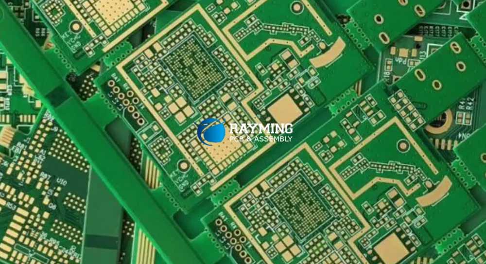
Gerber files are the standard format used to transfer printed circuit board (PCB) design data to manufacturers for fabrication. They encode copper layers, solder masks, silkscreens, drill data, and other information required to produce a physical PCB.

Opening and inspecting Gerber files is an essential skill for PCB designers. Reviewing the files before sending them out for fabrication helps catch any errors in the data. Understanding how to translate raw Gerber data into human-readable information is key.

This guide will walk through the basics of the Gerber format, the types of Gerber files, the tools available for viewing them, and how to open Gerbers in the leading PCB software. With the right knowledge, even novice users can learn to visualize PCB designs from the underlying Gerber files.

What are Gerber Files?

Gerber files use a specific CAD file format native to the Gerber scientific plotting device invented in the 1960s. They have since become a standard exchange format in PCB fabrication and assembly due to benefits like:

  • Vendor neutral data exchange
  • Capability to represent all fabrication data
  • Human readable text codes
  • Reliable validation tools

Some key facts about Gerber files:

  • ASCII text format describing PCB images in Cartesian coordinates
  • Contains codes for primitives like move, draw, flash apertures
  • Includes netlist info and various metadata
  • Individual files represent copper layers, silkscreens, solder masks, drill data, etc.

By combining multiple Gerber files together, manufacturers can fully reconstruct PCB designs. Next weโ€™ll look closer at the typical file types.

Types of Gerber Files

A complete PCB fabrication dataset will consist of multiple different Gerber files carrying specific design data. Here are some of the most common types:

File TypeDescription
Copper LayersThe conductive copper traces and shapes on each layer
Soldermask LayersThe insulating soldermask regions and openings
Silkscreen LayersThe visible silkscreen graphics and markings
Drill DrawingLocations and sizes of all drilled holes
Drill DataThe NC drill file with drill hole tools
Assembly DrawingsMechanical drawings showing PCB outlines, etc.
NetlistsConnectivity data for manufacture testing

Additional files like Inner Layer drawings, testpoints drawings, and scoring lines may also be included.

Knowing the purpose of each layer is crucial for understanding the PCB images when opening the Gerber files.

Why Open Gerber Files?

Before sending Gerber data to a PCB manufacturer, designers will want to open and inspect the files for multiple reasons:

  • Visual validation – Verify images match intended PCB layout
  • Error checking – Look for missing copper, silkscreen issues, etc.
  • Data validation – Confirm all necessary layers are present
  • Manufacturing review – Check for producibility issues like isolation, annular rings, etc.

By reviewing the compiled data files, errors and problems can be caught early before costly PCB fabrication begins. The ability to open and inspect Gerbers is therefore an essential skill for avoiding issues.

Tools for Viewing Gerber Files

There are a variety of options available for opening, viewing, and inspecting Gerber data files. Here are some of the most common solutions:

PCB Design Software

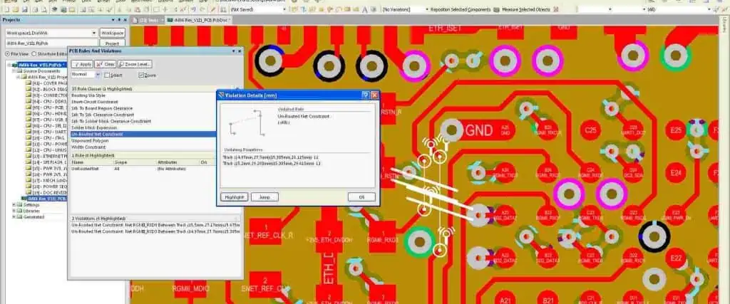
Most PCB design packages like Altium Designer, Eagle, KiCad, OrCAD, and others have native capabilities to import and visualize Gerber files. These tools allow validation directly against the source design.

Gerber Viewers

Standalone Gerber viewers like GC-Prevue and Kicad StepUp provide dedicated Gerber and drill file visualization. They render all layers and offer measurement tools, but lack editing capabilities.

Text Editors

Since they use ASCII text, Gerber files can be opened in text editors like Notepad or Sublime Text. This allows parsing the raw data codes but doesnโ€™t visualize images.

CAM Software

CAM toolchains like Genesis 2000 and Ucamco integrate various validation tools like DRC checking for deeper analysis of Gerber datasets.

Online Gerber Viewers

There are also various free online Gerber viewers that allow file uploads for visualization and sharing of designs. These are accessible to anyone with just a web browser.

In the following sections, weโ€™ll provide specific guidance on opening Gerbers across the leading options.

Opening Gerber Files in Altium Designer

Altium Designer is one of the most popular PCB design systems used to generate Gerber files. It also provides excellent built-in Gerber viewing capabilities:

  1. Select File > Import > Gerber File
  2. Choose the files and select import in single layer mode
  3. Files will appear as new layers in the CAM document
  4. Enable the desired layers in the layer tabs
  5. View the rendered images and measure as needed
  6. Validate against source PCB file if available

Additional functions like performing DRC checks, overlaying drill holes, and generating fabrication outputs are also available.

Opening Gerbers in Eagle CAD

Different software have different method to generate Gerber,EAGLE

The free version of Eagle CAD has limited support for Gerber files, but the premium version includes sophisticated viewing tools:

  1. Use the File > CAM Processor tool
  2. Under modes, choose to enter the CAM editor
  3. Import the Gerber files from the job panel
  4. organizing individual layers as needed
  5. Switch between layers to inspect images
  6. Validate against board file by overlaying layers

Eagle also provides an automated DRC tool for analyzing Gerber datasets.

Viewing Gerbers in KiCad

The open-source KiCad tool has an advanced GerbView utility for inspecting Gerber files:

  1. Launch GerbView from the KiCad main menu
  2. Use File > Load Gerber Files to import a folder of files
  3. Files will appear as layers in the layer manager
  4. Toggle layer visibility to inspect images
  5. Adjust transparency to overlay multiple layers
  6. Perform measurements and export images

KiCadโ€™s GerbView provides extensive options for manipulating, analyzing, and validating Gerber data.

Using Online Gerber Viewers

For quick online viewing, online tools like Pentalogix ViewMate offer straightforward Gerber inspection:

  1. Navigate to www.pentalogix.com/viewmate.html
  2. Drag and drop Gerber files onto the page
  3. Click the layers button to enable different files
  4. Pan, zoom, and measure the PCB images
  5. Optionally export images or share URL

Online tools provide easy collaborative viewing without any software install.

Tips for Inspecting Gerbers

When reviewing Gerber files, here are some useful inspection tips:

  • Check silkscreen layers for desired text and logos
  • Look for complete copper fills with no voids
  • Ensure adequate annular rings around plated holes
  • Look for any exposed copper that should be covered by soldermask
  • Verify board outlines, cutouts, notches all aligned between layers
  • Cross-check any layer misregistration with fab tolerance

Finding potential issues early prevents headaches once boards are fabricated!

Automating Gerber Inspection

Since manually screening every Gerber file is tedious, many designers utilize automation scripts for validation:

  • Script DRC rules validation on layers for potential violations
  • Programmatically check annular ring tolerances around drilled holes
  • Automate layer alignment checks between copper, silkscreen, and soldermask
  • Hash and audit design files for data integrity
  • Execute regression tests on new file generations

Automated checking provides peace of mind that Gerber data is valid before production.

Key Gerber File Insights

To wrap up, here are some key insights on working with Gerber files:

  • Gerber format encodes complete PCB fabrication data into various layers
  • Understanding typical file types provides context when viewing
  • Visual inspection validates designs and catches issues early
  • All leading PCB tools can import Gerbers for validation
  • Online viewers enable quick collaborative reviewing
  • Automation assists in verifying quality and validity of datasets

With the ability to properly open and inspect Gerber files, electrical engineers can have confidence their PCB designs will translate accurately into fabricated boards.

Frequently Asked Questions

What are some common problems found in Gerber files?

Typical Gerber issues include incorrect copper shapes, silkscreen misalignment, voids in copper pours, thin or missing annular rings, insufficient isolation between pads, and incorrect board outlines.

What does aperture mean in Gerber files?

Apertures define the shape and size of the drawing tool. Different aperture codes correspond to tools for drawing circles, rectangles, polygons, etc. These are then flashed to create the PCB images.

Can Gerber files be edited after generation?

While Gerber files are primarily intended as output files, some CAM tools do provide limited editing capabilities, like removing slivers or scraps. But more significant changes typically require modifying the original design files.

How can you validate drill data in Gerbers?

The drill drawing can be visually validated for proper hole locations. The separate drill data file is used by CAM tools to validate the specified drill bit sizes and hole tolerances.

Whatโ€™s the best way to learn to inspect Gerbers effectively?

The open source reference PCB โ€˜BeagleBone Blackโ€™ is commonly used in training. Comparing your own generated Gerbers against the reference validated data helps train an eye for spotting potential issues.

Conclusion

Understanding how to open and inspect Gerber files is an essential skill for avoiding costly mistakes in PCB fabrication. Whether using desktop PCB tools, online viewers, or automated scripts, reviewing Gerbers before manufacturing catches errors early.

This guide covered the basics of the Gerber format, typical file types, reasons for inspecting, leading viewing tools, and tips for effective validation. With the ability to visualize raw PCB design data, electrical engineers can take a proactive role in ensuring their creative visions translate accurately into physical boards.

PCB File:

A file that contains an electrical circuit board pattern is called a PCB file. The PCB stands for “Printed Circuit Board.” You do not require the computer program utilized to produce the file; many Windows application programs with PCB support are acquirable, and each can open up the printed circuit board pattern.

Your blueprint file will hold the mandatory info of levels and other things associated with PCB. Your PCB data file will contain information about all layers and their spread-eagling. Moreover, it will also hold information concerning holes and via sizing along with the lowest and uppermost silk layers.

Your maker will demand this data file to manufacture your electrical circuit design. This data file will state your trusted PCB attributes, finished copper, solder mask via the process, and additional details.

YouTube video

PCB File Formats:

At this spot, it is valuable to mention that your final file will not all of the time bear the .pcb file extension. It may be a PCB file or a Gerber file. Furthermore, each software system will have its particular file type. Frequently, you will run across .pcb files more than other extensions.

PCB design end product is the data files wanted by the makers for planning the PCB. Although operating on a PCB setup, you edit out a data file that is selective to your CAD software system. It is not a general file format, and the data it utilizes is unneeded to the maker. This is how you want to get a different kind of data file as you change the conventional into a physical, electrical circuit board. Almost every electronic gimmick is a PCB onto which the elements are automatically and electrically linked up by soldering. PCB pattern utilizes a CAD (computer-aided design) system. To physically understand the pattern, we must shift the cybernetic blueprint information to a photolithographic computer-aided manufacturing (CAM) system. As various companies typically create computer-aided design and computer-aided manufacturing systems, they must accord on a CAD-to-CAM information exchange format to shift the information. You can also open .pcb files online.

Which file format can you beget or export with a basic software system?

open brd file

In the concern for manufacturing PCB, you will frequently require to create a Gerber file format as Gerber file carries data concerning 2-D artwork that states the maker about the place of solder mask, copper, and so forth.

Thus, you might find out it hard to beget a Gerber file. It does not associate with internet connectivity, blueprint rules, or component libraries. You will require excogitating about distinct configuration details as creating a Gerber file.

As a whole, you will be able to abide by the following two steps for begetting a Gerber file:

  1. Search for a maker who will offer you directions for begetting a Gerber file. The directions will be as per the particular CAD software.
  • And then, you can utilize that CAD software to intent your printed circuit board.

All the same, this is not as effortless as it sounds. All the same, with practice, you will be able to master this piece of work. Further, you can avoid a malfunctioning PCB and held up manufacturing by cautiously following the directions. Well, you can try to open gbr file online it may help you out.

How do I open up a PCB file in Eagle and PCB file viewer?

  • Opening up a PCB file in Eagle Software:

Eagle is doubtless one of the popular software packages of an electronics engineer. Eagle is a PCB design software package and has created the contriving process a joyous one. Instantly, a question might come up in your mind concerning opening up a .pcb file in Eagle software, is it possible to open up a .pcb file in Eagle software? Or can we open gbr files in Eagle?

Unluckily, the .pcb file format is not associated with Eagle software. So, you cannot open up a .pcb file with Eagle, but you certainly can apply different software packages to do so. You can open the file with gerber viewer online free tool.

Furthermore, you will find a user script here that can change your file into something like that Eagle can open up.

  • Refreshing the PCB file in PCB file viewer:

When you have your wanted .pcb file, you require viewing it. Looking at it is determining to be sure that it has everything that you and your maker want. You can refresh your PCB files in a Gerber viewer. You can use the Gerber viewer online for free. It will assure that whatsoever you are posting is a suitable illustration of your pattern files.

Moreover, previewing the .pcb files will also make sure that your data files have been exported correctly.

How To open up or change Your PCB files from some other Software?

  • Eagle to Gerber:

Foremost, you will require opening up your PCB design data file in Eagle. This data file will hold a .brd extension. Later on, that, abiding by the following commands:

  1. Select “File -> CAM Processor.” CAM central processor instrument will open up to create your Gerber file.
  • And then, choose “File -> Open -> Job”.
  • And then go to your default option that is the cam folder of Eagle, choose “gerb274x.cam -> Open”.
  • At last, select the “Process Job” button to beget the Gerber files.

You are also able to open .brd files open. You can try to open .brd file online it might help you so you should not require downloading the software packages.

  • Altium to Eagle:

Fortunately, you will be able to import Altium data files in Eagle. You require to export your Altium blueprint file into ACCEL ASCII file format. Eagle then simplifies this information structure. You will need to tick on Import/File/Pad in Eagle and abide by the commands.

  • Changing Gerber Files (“.gbr”) to “.pcb” files:

For changing Gerber data files (.gbr) to Altium (.pcb) files, you will require to convert the data file extensions. For instance, if you have a peak layer Gerber file called “Layer1. Pho”, you can change it into an Altium file by converting its name to “Layer1.GTL.”GTL” file extension mentions Gerber Top Layer.

PCB files requisites:

Every PCB maker has a few requisites which you require to accomplish before positioning an order. The PCBs data file that you will propose to them must bear these requisites.

PCB design requisites:

FULL PCB MANUFACTURING Quote

As per to a few makers, Gerber files should let in:

  • Drill instrument listing
  • Silkscreen
  • Excellon drill data files
  • Solder mask
  • Internal layers with signs depending upon the pattern
  • Aperture / D-Code listing
  • Board draft
  • Readme file
  • Copper levels
  • Copper weight and insulator thicknesses essentials

You will as well come across a couple of makers who will accept aboriginal blueprint files of:

PCB drill file requisites:

Once again, the makers will demand you to present PCB drill files the accompanying way:

  • Possibly in Excellon format.
  • They had better not bear “G01”, “G54,” and “D” codes if opened up in a text editor.
  • They had better not hold some weird graphic characters; they must hold visible ASCII text.
  • If they are arranged properly, they will have sizing dispensed with “T” codes.
  • In that respect, there had better be a tool write-up holding the drill sizing.
  • Present them NC Drill File or fab graphics for cuts out and slots.
  • For a plated cutout or slot, you had better put the dimension on the drill level. Later on, mention an external layer pad bearing a minimal cutout or slot you would like to be plated.
  • For non-plated cutouts or slots, position them on the draft layer.

Electrical circuit board routing requisites:

Makers commonly get the thought about electrical circuit board routing out from the PCB draft.  You had better keep in mind the coming points while rendering your PCBs file:

During the routing out procedure, we will suggest you apply a copper back set of 0.020? It will assist you in keeping off the damage to copper dimensions. Some makers may as well permit you odd or circular shapes but with a few constraints. Then, once you have accomplished all the above and additional similar requisites, you are all fit to post an order. Exact requirements will hinge upon your makers. Just be sure to let in everything in your .pcb file.

Final Verdict:

A PCB data file is a primary thing that you should bear for manufacturing your electrical circuit design. Here all the details related to a file are discussed. Like what is a PCB file? How is it open up? What are the requirements to open PCB files? And so forth. It would help if you were sure that your PCB files are accomplishing your maker’s requisites. By following the above instructions, you can open your PCB files through the different software mentioned above. It is not so easy but not too tricky it only required practice.

About 94v0 Circuit Board You Should Know

94v0 Circuit Board

You may wonder what a 94v0 circuit board means. Sometimes, some people (engineers and other practitioners) ask about the relevance of this board to their electronic jut. Or you begin to ask why one should selectively pick them over the typical PCBs? All skepticism about the 94v0 circuit board is a result of inadequate information about it.

You need very strong and reliable devices that can stand the test of time. Engineers need them for tough environments and varying temperatures. As a result of this, several circuit engineers have thought of means to compute and assess materials to copy out PCBs. As there is an increase in curiosity, there is the need to decide on the structure that would grade some testing of various PCB design materials. In this article, you shall read a thoroughly researched write-up on what a 94v0 circuit board entails. In the end, you shall see what relevance the board has to your profession.

What Does 94v0 Stand for?

It is very crucial to understand everything about this circuit board. This 94v0 has to do with the flammability standard test. Your devices should be able to withstand a harsh environment. The UL 94 pays attention to the standard of the flammability of the plastic matter of components in any device. It has to do with the testing of flammability of appliances.

The UL 94 simply has to do with the plastic measure of the extent to which it can be flammable. The flammability quality or grade of the plastic is as indicated in the US by the Underwriters Laboratories. It is simply connected to the grade at which the material can put out fire. The flammability standard matters so much.

 Once anything ignites the material, it can further spread flames. The UL 94 is in compatibility with the IEC 60695- 11- 10 as well as 60695-11- 20 with the ISO9772 and 9773. Sometimes, vertical wire burn (VW- 1) evaluation or ranking is incorrectly endorsed with the UL 94. However, it is mostly portrayed by the UL 1581. This is the grading for cables, flexible cords as well as wires by the reference standard. For the flammability of the plastic, some are low flame retardant while others may be high fire retardant.

The testing is mostly carried out on the scale of a 127 mm by 127 mm sample of the lowest amount of confirmed thickness. The following below shows the flammability degrees of some materials.

HB: This has to do with the low speed of consumption by flames or radiation. Its overheating is gradual and burns slowly on some horizontal samples. Its burning rate could be within the range of 76 mm. However, its burning fades away before getting to at least 100 mm.

V-2: This burning ceases at about 30 seconds and some leak or drops of fire fragments could be permitted. The burning is on some vertical samples.

V-1: For this, the burning ends at about 30 seconds. This is often on some vertical samples. Note that leaks of flaming fragments can come up. No inflammation in this scenario.

V-0: This is another form of burning on some vertical samples. However, the burning ceases about 10 seconds before the duration ends. The drips from flaming come up. This can come up as long as there is no inflammation.

5VB: For this, the burning ends within some seconds. This is mostly about 60 seconds of burning on some vertical samples. However, some holes can begin to come upon a plaque sample.

5VA: At this burning period, there are no drops of flaming permitted. However, the burning ceases about 60 seconds within a period of flaming. It is mostly on the vertical samples just like other burning specimens. Note that the plaque sample may not necessarily progress into having some holes.

What Do I Need To Know About the 94v0 Circuit Board?

94v 0 pcb

We have discussed what the 94v0 means. The UL 94 has to do with some circuits present at the Printed Circuit Boards. To discuss this more elaborately, the 94v0 circuit board has circuits engraved on the PCBs which must have gone through some UL 94V-0 testing in relation to its flammability. Note that these kinds of circuits are very optimal or perfect for creating austere electronic equipment.

 Also, it is for the production of equipment that can absorb harsh environmental conditions. These devices are durable and highly powerful. Circuit engineers ensure that the circuit board is a major component in manufacturing electronic equipment.

The 94v0 circuit board has some temperature control or modulation panels. This always helps to regulate heated temperature. In a way, it prevents any form of overheating. This is very important to the PCB. The 94v0 circuit board has some varying degrees of thickness. This is the same way it has its varying sizes. The reliability testing must have been carried out before using it. This is to know how parts of the plastic matter can absorb harsh environmental conditions.

 Some of the other testing includes thermal power test and shock test, solder testing, fixture testing, and flying probe regulations among others. One must ensure that all the parts of the board are well soldered. Also, the proper installation is paramount.

A very good 94v0 board must be effective in many ways. It must serve the purpose of which circuit engineers made it for. It is needed for safety in electronic devices. That is why it goes through flammability standard testing.

The circuit board could be available in different dimensions. It is paramount to consider the various kinds of PCBs that are available. This will enable you to know that some circuit boards could either be single-sided PCBs or double-sided PCBs.

As a result of the varying needs of users, there are different kinds of PCBs. One interesting thing is that the P4v0 circuit board is important in every electronic device. They undergo different stages of production as well as various application prerequisites or conditioning. When choosing your PCB, it is crucial one considers the space needed. Also, you should opt for the one that has electrical stability capacity.

Single-Sided PCBs

The printed circuit board has its different types. Among them is the single-sided one which is quite common. Unarguably, this is the most popular type among PCBs. Above its substrate lies the individual conductant copper stratum. One unique thing about it is that the electrical parts are positioned at a location right in the board.

The whole engraved circuit is seen at the other end. The conductants do not extend over as a result of just a conducting stratum it has. It is fit for underslung density design prerequisite. These single-sided PCBs are seen in some low-cost equipment. These include timing circuits, calculators, and lighting boards.

This kind of PCB has some merits for users. It is not difficult to produce. This is why manufacturers find it very easy to produce. Also, it saves cost. It is not the type that you get at high rates. It is good for some underslung density designs. It is very simple to fix when it gets damaged. Lastly, it is never difficult to design. This is because it has just an individual conductant layer.

Double-Sided PCBs

This is another kind of PCB. Copper is mostly added to the layer above as well as the underneath of the board. This is at the sides. From each side, it can be possible to connect the metal parts through the hole. Circuit engineers use this kind of PCB in devices that are stronger like amplifiers, UPS systems, phone systems, and several others. One advantage of this type is that it is more flexible than the single-sided PCB. Also, there is a larger circuit density in it.

There are certain factors that could be responsible for PCB failure. Yes, the PCB can fail outrightly. This happens on certain occurrences. One major factor responsible for this is the environmental determinant. This factor is the result of particles like dust. Dust is one environmental factor that can badly damage the PCB. Other environmental factors include heat, drops, and moisture. Power surge as a result of overloading badly affects the PCB. This has over time had a terrible effect on the printed circuit board.

More on the 94v0 Circuit Board

The 94v0 circuit board diagram shows the components of the circuit board. It is available online for users to see what each part looks like.

The 94v0 PCB goes through a series of fire tests to determine if it can withstand fire. This shows if the electronic equipment meets the set standards for fire protection of devices.

Fr4 94v0 is also a determinant of the circuit board. It also shows the manufacturer’s taste for a quality board. This is because it must be durable and highly powerful.

Conclusion

The 94v0 circuit board is for the simplicity of life. It makes it safer to use devices because it goes through a series of flammability standard testing. It is both present in smaller and larger devices. It makes it possible for flexibility. Also, it is cost-effective. One does not necessarily have to spend so much on it. It is the belief that from this article, people can now understand what this circuit board entails.

How To Design A High Current PCB

High Current PCB

Introduction

Printed circuit boards (PCBs) are at the heart of countless electronic devices and products. For many applications, PCBs need to safely and reliably handle significant amounts of electrical current flow. Designing PCBs for high current operation requires special considerations during schematic capture, component selection, layout, and analysis.

This guide will provide a comprehensive overview of best practices for creating high current PCB designs. Weโ€™ll cover key factors like choosing the right traces widths, utilizing multiple layers, managing heat dissipation, minimizing inductance, and more. With the right techniques, you can create robust and optimized high current PCBs. Letโ€™s get started!

High Current PCB Design Guidelines

heavy copper pcb

Here are some of the most crucial guidelines to follow when designing a PCB for high current operation:

Use Appropriate Trace Widths

The first requirement is using PCB copper traces wide enough to handle the expected current without overheating. Some key calculations include:

  • Use Ohmโ€™s Law to convert current to amps and target trace resistance
  • Determine suitable trace widths based on copper thickness and ampacity tables
  • Adjust widths based on desired temperature rise and heat dissipation needs

Wider traces are almost always better for higher current capacity.

Enable Thermal Relief and Heatsinking

Managing heat buildup through thermal relief and heatsinking is critical. Key strategies include:

  • Add thermal spokes or planes connected to high current traces
  • Use thermally conductive pads and vias
  • Connect traces to copper polygons or metal pins for heatsinking
  • Ensure adequate clearance around heat-sensitive components

Utilize Multiple Layers and Planes

Distributing current across multiple board layers provides more capacity and reduces heating. Consider:

  • Use a 4+ layer board for inner power and ground planes
  • Alternate signal and power/ground layers
  • Use vias to connect layers for current sharing

Select Low Resistance Components

Choose components rated for high continuous current when possible. Look for:

  • High-power resistors, capacitors, diodes, regulators etc.
  • Components with low ESR (equivalent series resistance)
  • High current inductors if needed
  • MOSFETs, IGBTs, thyristors for switching

Reduce Inductance With Short Paths

Minimizing parasitic inductance improves transient response and reduces voltage spikes. Tips include:

  • Use the shortest possible traces for power flows
  • Avoid right angle turns; use curved and 45ยฐ traces
  • Interleave input and output power paths
  • Use ground plane layers for current returns

Perform Analysis and Simulation

Verify the design through analysis like:

  • Thermal simulation to check temperature rise
  • Current density simulation to identify hotspots
  • Power plane analysis for optimal decoupling
  • SPICE transient analysis to characterize switching

Next, weโ€™ll explore each of these guidelines in greater detail, including trace width calculations, heat management, component selection, and analysis techniques tailored specifically to high current PCB design challenges.

Calculating Appropriate Trace Widths

PCB-Trace-Width-Calculator

The starting point for any high current PCB layout is determining the right trace widths for the expected current levels. Letโ€™s walk through the essential calculations involved.

Gather Key Parameters

First, identify the key parameters that factor into trace width:

  • Target current – The maximum steady state current for the trace, typically in amps. Know the worst-case scenario.
  • Allowed temperature rise – How much heating above ambient can be tolerated? 20ยฐC and 40ยฐC rises are common.
  • Copper thickness – Standard PCB copper thickness like 1 oz, 2 oz, etc. Thicker copper has higher ampacity.
  • Target trace resistance – Typically below 50 milliohms for high power; lower is better.
  • Ambient temperature – The external environment temperature.

Use Ohmโ€™s Law to Find Target Resistance

With the target current known in amps, we can use Ohm’s law (R = V / I) to calculate the resistance needed to avoid excessive voltage drop:

Target Resistance = Target Voltage Drop / Target Current

For example, allowing a 100 mV drop with a 15A current flow means the trace resistance should be around 6.7 milliohms.

Lookup Trace Width Based on Desired Ampacity

Next, use ampacity tables to find the trace width needed to achieve the desired ampacity (current carrying capacity) without overheating.

For instance, for 2 oz. copper with a 20ยฐC rise, 15A requires around a 270 mil (0.27″) trace width. Allowing some margin, a 300 mil trace would be selected.

Ampacity varies based on copper thickness, temperature rise, and other factors. Refer to published tables or calculators to determine appropriate widths.

Account for External Thermal Factors

Environmental conditions and the presence of heatsinking or airflow should also be considered:

  • Increase width at higher ambient temperatures
  • Decrease width if adequate heatsinking is available
  • Adjust for enclosed vs open air environments

Ample trace widths are advisable when possible for high current. Now letโ€™s look at managing heat generation.

Managing Heat With Thermal Relief and Heatsinks

Thermal Relief PCB
Thermal Relief PCB

No matter how wide the traces, significant heating can still occur when conducting high current. Effective thermal management is crucial to ensure the PCB remains within desired operating temperatures for nearby components and materials.

Provide Thermal Relief

  • Thermal relief* refers to design techniques that help dissipate heat away from traces carrying high current:

<!—->

  • Use thermal spokes – radial copper shapes connecting traces to plane layers
  • Surround traces with copper pours for better heat spreading
  • Place thermally conductive vias alongside traces as โ€œthermal viasโ€
  • Use wide, isolated copper regions as heat sinks

Incorporate Heatsinking

Heatsinking refers to dissipating heat by conductively coupling the high current traces to materials with higher thermal mass. This keeps traces cooler under load. Strategies include:

  • Connect traces to large copper regions or thermal pads
  • Link to thicker metal pins, cables, or external heatsinks
  • Embed metal cores or inserts to absorb heat
  • Ensure air flow over board for convection cooling

Proper use of thermal relief and heatsinking prevents excessive trace temperatures during high current operation.

Leave Adequate Clearance Around Heat-Sensitive Components

Ensure that heat generating traces have sufficient clearance from components like electrolytic capacitors that have tighter temperature limits. Use space and isolation to shield sensitive nearby parts from heating effects.

With smart thermal management, the PCB can stay cool even with very high current flows.

Harnessing Multiple PCB Layers

Capitalizing on the use of multiple PCB layers is key for accommodating high current flows. Letโ€™s look at best practices.

Use 4+ Layer Boards

High current PCBs should utilize at least four layers: top and bottom signal layers, and power and ground plane layers internally. This provides more area for current conduction while also helping manage heat.

Additional layers can be added for very high current capacity or to incorporate shielding layers. But four tends to be the minimum for high power applications.

Dedicate Layers for Power and Ground

The internal layers should be dedicated as whole planes for power and ground distribution. This gives maximal current capacity.

Use a grid of vias to connect the planes to surface traces for sharing current across layers.

Alternate Signal and Plane Layers

Alternating signal layers with power/ground layers is ideal for high current stacking:

Copy code

Top Layer (Signal) Plane Layer (Power) Layer 2 (Signal) Plane Layer (Ground) Bottom Layer (Signal)

This allows signals to have low impedance returns through adjacent planes while also simplifying routing.

Incorporate Vertical Layer Transitions

Utilize vias, component pads, and other vertical interconnects to transition current between layers for optimal distribution. The goal is to maximize utilization of the full PCB volume.

A multilayer approach with dedicated power planes is ideal for meeting high current demands.

Component Selection Considerations

extreme copper pcb

In additional to PCB traces, the electronic components used in a high current design must also meet power demands. Letโ€™s review key selection factors.

Choose High Power Resistors

When using resistors, choose appropriately rated power resistors up to several watts. Requirements include:

  • Adequate wattage rating for expected power dissipation
  • Sufficient heat sinking properties
  • Non-inductive type for high frequency applications

Select Capacitors With Low ESR

For capacitors, low equivalent series resistance (ESR) is key. Prioritize types like:

  • Electrolytic capacitors designed for high ripple current
  • Polymer capacitors that withstand heat and surges
  • Low ESR ceramic capacitors for decoupling

Avoid small form-factor capacitors not rated for power use.

Consider High Current Inductors

Standard signal inductors saturate at higher currents. For inductors in power circuits:

  • Choose ferrite, iron powder, or toroidal inductors intended for power use
  • Select inductors with higher saturation current ratings
  • Allow margin above peak current demands

Use MOSFETs, IGBTs, and Thyristors For Switching

When using semiconductors like transistors or ICs for high current switching applications:

  • Choose components rated for adequate continuous and pulsed current
  • Watch peak current, rise time (di/dt) and RDSon specifications
  • Use TO-220, TO-247, or other power packages
  • Look for automotive or motor control rated parts

With robust components selected for the expected current levels, the circuit design is much more likely to operate reliably under high power demands.

Minimizing Parasitic Inductance

For high current PCBs carrying pulsed or AC currents, the parasitic inductance of traces and loops can lead to voltage spikes or ringing. Careful layout is key to minimizing inductance.

Use the Shortest Possible Traces

The number one rule is to make high current traces as short and direct as possible:

  • Avoid meandering, zig-zag, or tightly curved traces
  • Use 45 degree angles instead of 90 degree bends when needed
  • Tightly couple input and output paths together

Shorter traces proportionally reduce parasitic inductance.

Avoid Loop Areas

Minimize the enclosed area of high di/dt current loops. Strategies include:

  • Use ground plane layers for tight signal returns
  • Interleave input and output paths side-by-side
  • Eliminate loops by using low-inductance bidirectional flow

Loops allow magnetic flux buildup โ€“ smaller loops give lower inductance.

Use No-Connect Copper Fills

Flooding non-critical regions with copper fills reduces loop areas. The fills act as continuations of the ground planes without forming shorts.

Simulate Current Density

Current density analysis can reveal localized areas of higher di/dt and associated inductance for mitigation.

With careful layout practices, parasitic inductance can be designed out of the PCB early for robust high current performance.

Verification Through Analysis and Simulation

The final step is leveraging analysis techniques like thermal simulation, power plane analysis, and circuit simulation to verify the design before manufacturing the PCB.

Thermal Analysis

Thermal simulation confirms the PCB will remain within acceptable temperature limits under expected current loads and ambient conditions:

  • Perform steady state thermal analysis to check temperature rise
  • Run electrothermal analysis to account for interdependencies
  • Verify thermal management features are working as intended

Power Integrity Analysis

Power integrity analysis ensures clean power distribution with minimal noise:

  • Run AC analysis to optimize decoupling capacitor placement
  • Check for adequate target impedance levels
  • Identify resonance risks from planes and capacitor banks
  • Verify power stability for all load conditions

Transient Circuit Simulation

SPICE and other circuit simulation techniques characterize performance:

  • Simulate switching behavior and voltage/current waveforms
  • Check for issues like ringing or electromagnetic emissions
  • Account for parasitic capacitance and inductance
  • Assess worst-case transients at high di/dt

These analysis flows validate the design early, before any high current issues appear!

Example High Current PCB Designs

To make these concepts more concrete, letโ€™s walk through a few example high current PCB implementations.

High Power LED Driver

Here is an LED driver PCB designed for constant current output up to 5A for high power LEDs:

  • Uses 4-layer board with power and ground planes
  • LED terminals use wide 500mil traces
  • Vias connect layers for thermal relief
  • Short, direct paths used for current loops
  • Components rated for high power use

High Current Buck Converter

This 15A buck converter steps down voltage for motor drives and other loads:

  • Large high current tracks and polygons
  • Thermal relief techniques used throughout
  • Low ESR capacitors plus ceramic bypass
  • Short, coupled inductor traces
  • Robust MOSFETs and minimal parasitic PCB inductance

High Power Audio Amplifier

Here is a stereo audio amplifier PCB supplying over 50 watts into 4 ohm speakers:

  • Multiple ground plane layers for noise isolation
  • Beefy traces bringing power to amplifiers
  • Thermal vias help heatsink output devices
  • High current resistors used for gain setting
  • Simulation confirms low THD and clean power delivery

These examples illustrate the techniques explored in this guide applied to real-world high current scenarios.

Key Takeaways

To recap, the major best practices for high current PCB design include:

  • Use appropriately sized traces based on expected current
  • Incorporate thermal management strategies
  • Utilize multilayer boards with power/ground planes
  • Select components rated for higher current
  • Minimize parasitic inductance through layout
  • Verify the design through advanced analysis

Combining these practices allows you to create reliable, optimized PCBs for high power applications able to safely handle substantial currents.

The demand for current capacity in electronic devices keeps increasing. By mastering high current PCB design techniques, electrical engineers can meet the needs of the latest LED drivers, battery systems, motor controllers, power converters and other high power electronics.

Frequently Asked Questions

How thick should traces be for 10A current?

For 10 amps, a good starting point is 500mil wide traces on the outer layers using 2oz copper. Wider traces, thicker copper, and inner plane layers can provide additional margin.

What is the maximum current for a 4-layer PCB?

There is no fixed limit, but practical capacities with good design are 30-50A for inner power plane layers, and 15-30A for outer signal layers. More layers proportionally increase capacity. Proper thermal management must be incorporated.

When should heatsinks be used on a PCB?

Heatsinks are recommended whenever localized heating could exceed desired temperatures in a high current region. Large copper planes, thermal pads connected to traces, and external heatsinks help ensure components and materials remain within safe operating temperatures.

How can I reduce inductance for high di/dt currents?

Use the shortest possible traces, interleave input/output paths, utilize ground planes for returns, eliminate loop areas, and flood unused areas to reduce partial inductance. Circuit simulation can also quantify parasitic inductance effects.

What type of analysis helps verify high current PCB performance?

Thermal simulation confirms temperatures remain in check. Power integrity analysis verifies clean power delivery. Transient circuit simulation models high di/dt effects. And signal integrity analysis can check for crosstalk issues. Advanced analysis gives high confidence prior to manufacturing.

Conclusion

Designing printed circuit boards for high current operation requires paying special attention to trace widths, thermal management, layout techniques, component selection, and analysis processes. Using the best practices described in this guide, PCB designers can create robust boards able to handle up to 50A or more of continuous current when properly engineered.

Key takeaways include using adequately sized copper traces, incorporating thermal relief and heatsinking, utilizing multiple PCB layers, choosing components rated for higher currents, minimizing parasitic inductance through careful layout, and leveraging simulation tools to verify the design.

With the growing demand for power electronics, high current PCB expertise is becoming increasingly essential. By following the guidance in this article, electrical engineers can develop expertise in laying out PCBs that perform reliably under high current loads. The ability to design boards with 10A, 20A, 30A or higher capacity takes practice, but by combining the right design processes, PCB engineers can master creating high power circuit boards ready for the most demanding industry applications.

How to become a PCB Engineer ?

PCB Engineer

Printed circuits got famous during the 1950s and the requirement for PCB design engineers to make PCB format designs for electronic circuits took off. Initially, PCB ideas were designed, or “spread out,” on a drafting circuit board at four or even multiple times the real size utilizing tape, blades, stickers, and a consistent hand. When finished, those drawings would be reproduced in video form utilizing a reduction camera, and that film would be utilized to make the PCB tooling at the creation shop. Today inflexible flex PCB format is done on cutting edge Computer-Aided Design frameworks (CAD), they use the output to make the PCB tooling.

YouTube video

The PCB layout engineer will make the models that will be remembered for the print board inside the CAD framework. Then, they made the board design inside the CAD framework utilizing the impressions that have been made. When the entirety of the necessary impressions has been set on the board, they will associate the entirety of the electrical associations utilizing lines that address metal in an interaction called follow steering.

A decent PCB creator is also a process engineer, computer guru, manufacturing expert, and electrical engineer. Generally, notwithstanding, a board design engineer sees past the lines and states of parts on their PC screen to picture the last use of the PCB design. A decent PCB manufacture can make something from nothing while at the same time tackling various riddles.

Education required to be a PCB Designer?

Numerous designers are spreading out their PCB today. To turn into an electrical designer or a mechanical specialist, you will require a BS in those fields. Generally, PCB layout engineers design the board instead of “engineer” segments of the board or circuit boards. Accordingly, the instructive foundation contrasts in a few.

There is no degree committed to PCB manufacturing or PCB design for the individuals who are doing PCB format explicitly. You will likewise find that there are as yet numerous places that do not need the PCB creator to have a level of any sort. Nonetheless, you will have much better accomplishment as a PCB design engineer with experience or a degree that remembers courses for hands-on printed circuit board work, electronic design, computer-aided design, drafting, or other related study spaces. As PCB design becomes more unpredictable, more organizations will require degrees for their PCB model fashioners.

Many PCB declaration courses are useful with the guidelines for how to turn into a PCB design engineer. A few organizations offer explicit fast or multi-facet CAD instructional PCB design courses. Additionally, the IPC Certified Interconnect Designer (CID) course is an outright advantage for the new PCB architect.

Numerous specialists need to be decent PCB cam engineers; however, they come up short on the best way to go about it. It isn’t easy to understand what all means are required, which everyone can acquire.

Essential skills for a PCB design Engineer

pcb design engineer
  1. A detailed design review process

Design audits are essential to make the first time right design. The actual originator finishes the first. Then, at that point, the next survey ought to be finished by the equipment engineer. Afterward, the last audit by another qualified autonomous architect or an outside expert would be great.

  • 3D Model/Mechanical Design

These days a large portion of the PCB Design programming gives an approach to add 3D models of the segments and perceive how the PCB will look after it gets made and segments are amassed. Utilizing 3D models for every part, any issues identified between segment dividing and so on could be distinguished right on time during the design stage itself and helps save PCB updates exertion, cost, and time. Once in a while, it serves to do few models of PCB with connector rapidly, and so forth. Then perceive how PCB will look like and design for a mechanical nook, if all that will fit in or not, how it will resemble, and so on

  • PCB Design Rules

There is numerous normal design rule which needs to follow while designing a PCB. They fall under the accompanying class:

  • Design for assembling rules like track width, freedom, through/cushions size, drill size, and so on.
  • Design for a test like what all contemplations are required to test the sheets is made conceivable.
  • Considerations for power integrity
  • Considerations for thermal integrity
  • Noise decrease, EMI/EMC contemplations, signal integrity rules
  • General rules
  • PCB Layer Stack-up

When designing a multi-facet board, an unmistakable comprehension of the PCB layer stack is basic, interestingly right design.

  • PCB Design Software

Next is acceptable information on managing PCB design programming. One should know how to review via Gerber viewer tools, generate Gerber, create a component library, PCB layout, component placement, and draw schematic. There are numerous PCB design programming accessible on the lookout. It is prudent to pick the one which is broadly utilized in the business.

  • Basic knowledge of PCB

PCB is only a fiberboard that keeps hardware segments together in a most upgraded space and gives an electrical association. It is excellent to know how it is a part of power designs, vias, pads, tracks, electronic design, and so forth. Likewise, how these PCBs are fabricated. It aids in understanding many design rules which are straightforwardly identified with assembling or the actual nature of PCB.

  • Basic Electronics

PCB is exceptionally key to any hardware design, so excellent comprehension of electronic parts, it is interfaced, is essential. If you truly need to be an extraordinary board design engineer, information on electronic parts is significant. It closely resembles how an embedded firmware designer should realize the installed equipment to be a decent embedded design engineer.

Fundamental this an amateur PCB designer should consider

  • Tape-out:ย Compiling the entirety of the information in an arrangement that is appropriate for manufacture and gathering. A decent bet is that all that changes, except for the tape-out date. Documents are regularly broken out among creation and assembly. If you finished in a hurry which is very conceivable, go through and eyeball everything again.
  • The Design Review:ย Be prepared to clarify any choices you made in getting to the ideal format. It is seldom hard to work with one individual. By far, most have good intentions. Blend in a Digital and an Analog sort, and you can be in a back-and-forth. Bigger outfits will have a specialist for everything. You get an opportunity to sharpen your feline crowding abilities.
  • Drafting:ย Notes, measurements, and subtleties like opening outlines and stack-up charts are an indispensable piece of each report bundle. It is notwithstanding the real work of art layers. Metal layers, solder masks, and ink layers make up the heft of the craftsmanship. Information that is not essential for the board that you are additionally liable for incorporates a stencil for the weld glue affidavit and a document that drives the pick and spot machine.
  • Design Rule Checking:ย There will be many limitations that catch the ostensible calculation of the force area and any electrical properties related to different associations. Follow width, length, and separating are the primary concerns; however, numerous nuances are required as the design intricacy increments.
  • Place and Route:ย The primary design work begins with a board diagram and a netlist that pulls in the library and the rationale. Floor designing is the initial step. Deciding the best stack-up is a nearby second. As a rule, these qualities will go through certain emphases.
  • The Library:ย Any new parts should be represented. If your organization has an administrator, you may be sitting tight for certain impressions. Try not to allow that to keep you from getting to the basic pieces of the design. In case you are doing your own, benefit as much as possible from it. A ton of the dialect is prepared into the information sheets past the impression chart.
  • The Kick-off:ย Somebody needs a board, and you landed the position. Expect an information dump and be prepared to give a time of delivery. It appears to be reasonable to sand-bag if something turns out badly. That is a non-starter. They need an ideal situation that you will change as you go. Set a couple of achievements to remain on track. If you need to stay close by, you will execute the arrangement.
  • Getting the Job:ย Interviews can be extreme. Working will help you make the necessary networks with professionals in the field. You will also gain experience that you would otherwise not have found anywhere else.
  • The pioneers:ย Names like Ohm, Gauss, Coulomb, Joule, Volta, Ampere, Henry, and Faraday might be familiar. Likewise, set aside the effort to look into Gustav Kirchoff, who based on Georg Ohm’s work. That prompts Maxwell’s conditions and opens the establishment of hardware.
  • Education:ย Not just gadgets yet additionally basic geometry, mathematics, and physics. Extraordinary relational abilities are an absolute necessity. There is a touch of dramatic artistry engaged with overseeing assumptions. A degree was not constantly needed. You can figure out how to open a few doors following a half year in an exchange school.

The Future of a PCB Designer

The need to design current and to develop PCB advancements is developing. With increasingly more gadgets, for example, IoT getting conspicuous in regular day-to-day existence, the eventual fate of electronic design is exceptionally brilliant. In any case, the pool of experienced PCB makers is contracting as numerous board design engineers are moving toward the time of retirement. The business needs more PCB design engineers, and those that are now included are detailing that their pay and occupation fulfillment is on the ascent.

Do you have an enthusiasm for making things and making them work? Provided that this is true, then, at that point, spreading out printed circuit board designs might be the thing you are searching for. If you are prepared to begin a vocation as a PCB Designer, investigate Altium. Altium Designer is PCB design programming made for architects and PCB creators to make a-list PCB designs. Not exclusively will the product assist you with all parts of your design, yet Altium offers to prepare on programming will assist you with getting down to business.

What is FR5 PCB ?

fr5 pcb

Why are Printed Circuit Boards important?

Electronic items/appliances become functional due to Printed Circuit Boards. These PCBs are made of non-conducive material (the substrate or physical, insulating structure that holds the traces and components on it) covered in copper. PCBs have electric pathways connecting the different electronic components to each other through pads, traces, lines, and other features etched onto the copper plating.

PCBs are used in electronic devices and appliances across many different sectors, from handheld consumer devices to huge machinery and heavy parts. This blog entails details about the FR-5 as PCB substrate and why it is great for your PCB production needs.

Using high quality materials promotes longevity and performance of printed circuit boards. The FR5 Laminateย is a NEMAcertified board, known for its immense strength, chemical resistance, excellent electrical properties, and low moisture absorption capabilities. Its natural color is a yellow-green-tan blend, and it is made of fiber-glass fabric reinforced with high temperature epoxy resin binder similar to G10 / FR4. As you read along, you will receive more information about PCBs in general and FR-5 in particular.

Types of PCBs

PCBs can be differentiated according to their flexibility, number of layers, frequency, and substrate used. Some popular types are discussed below.

PCBs Types according to Flexibility

They can be:

Rigid PCBs are solder masked during production, while flexible PCBs are usually overlaid or cover-layered to protect exposed circuitry. The rigid flex combines the flexibility and lightweight of flex PCBs with the strength of rigid PCBs. Its small size makes it perfect as a space-saving circuit board. FR-5 is a rigid PCB.

PCBs Types according to Number of Layers

PCBs are designed and manufactured in many ways, dependent on their use as:

  • Single-sided (one copper layer). These PCBs are used for simple circuits, as sensors, power sensors, relays, and electronic toys.
  • Double-sided (two copper layers on both sides of one substrate layer). These PCBs are used in mobile test equipment, power monitoring, amplifiers, phone systems, and many other applications.
  • Multi-layered (inner and outer copper layering, alternating with layers of substrate). They are used in high speed circuits as they offer better spacing options for conductor pattern and power.FR-5 falls under this category.

PCBs Types according to Frequency

  • High-Frequency PCBs which are used in the frequency range of 500MHz โ€“ 2GHz. These PCBs are used in for communication systems, microwave PCBs, micro-strip PCBs, etc.
  • Aluminum backed PCBs are used in high power applications, as the aluminum dissipates heat. They are great for applications requiring high mechanical tolerance such LEDs and power supplies, because they offer high rigidity and low thermal expansion.

PCBs Types according to Substrate

PCBs are most often made as substrate, copper, solder mask, and silkscreen. PCBs substrates come in a large variety of options. The most popular substrate of a printed circuit board (PCB) is a thin board made from fiberglass, reinforced with composite epoxy resin, or other laminate materials with a copper foil layer on one or both sides: FR-4 and FR-5 PCB Substrate Materials. However, for classification purposes, there are three major types of materials used for fabrication of PCBs:

FR-5, FR-4 PCB Substrate Materials 

These both are the most common materials used in PCB manufacturing. FR-5 and FR-4ย substrates are made of woven fiber glass reinforced material and a flame-resistant epoxy resin binder. The epoxy used is flame retardant and water resistant, and provides a notable ratio of strength to weight. Lastly the tensile strength of both is very high.

PTFE (Teflon) PCB Substrate Materials

PTFE is a plastic-like material used for high speed, high frequency applications because it does not offer resistance in conductivity. PTFE is very lightweight and flexible, making it suitable for tight tolerance applications. It is also strong and flame resistant, versatile and provides temperature stability.

Metal PCB Substrate Materials

Metals such as iron, aluminum, and copper, amongst others are still used in PCBs because they allow easy integration of components in Surface Mount Technology (SMT). They have a long product life and provide mechanical durability.

The FR-5 Features and Advantage

fr4 PCB vs fr5 pcb

In order to understand the benefit of using the FR-5 PCB, here are some of its noteworthy features.

Moisture Absorption

Moisture can greatly lower the quality of lamination, solder mask, metallization, and production process of PCB board manufacture and assembly. Dampness and humidity inside a multi layer PCB also reduces the glass-transition temperature (Tg) resulting in excess thermal stresses that can damage the board or components causing PCB failure. In the FR5 PCB, the moisture absorption is low making it a prime choice when selecting a PCB material.

Resistance

The FR5 circuit board can resist many things, which lowers the risk of faulty PCB functioning or PCB failure. FR5 PCB is impressively Heat and Radiation Resistant, and Chemical Resistant. It also has a low dielectric loss.

Mechanical Properties

We have already mentioned that FR-5 has low dielectric loss. This means it has high dielectric strength, which can be defined as the maximum voltage needed to produce a dielectric breakdown through the insulating material. FR-5 also has High Tensile Strength which indicates the stress threshold that can be applied to it before it breaks. Its High Flexural Strength is its ability to resist breaking when pressure is applied. These features determine its application and ensure its longevity.

Excellent Performance

Investing in the FR5 PCB is the right thing to do considering the excellent performance. One way of monitoring of the FR5 PCB performance is during the lead-free soldering process. It can be easily applied to the following fields:

  • Circuit Board Holders
  • End Plates
  • Solder Frames
  • Antennal Isolators
  • Test Boards
  • Electrical Equipment
  • Aerospace


Why are FR-4 and FR-5 popular as PCB substrates?

There are many substrate materials used in PCB production. NEMA (National Electrical Manufacturers Association, USA) classification has named a group of laminates as FR. FR stands for Flame – Retardant or Fire Resistant and signifies that the material complies with UL94VO, and the ensuing numbers 1 till 5 differentiate the different materials in the same class. The group comprises of FR-1, FR-2, and FR-3, FR-4, and FR-5, and are popularly used for single sided, double sided and multilayer printed circuit boards, dependent on compliance with strict requirements for mechanical strength.

From single to multilayer PCBs (going up to 40 to 50 layers of substrates and copper layering: theoretically even 100 layer PCBs can be made)  FR-1, FR-2, and FR-3 materials have all been used to manufacture PCBs. FR-4 and FR-5 are used the most. Despite the fact that FR2 and FR3 materials are cheaper than FR4 and FR5 PCB materials, PCB designers prefer these more expensive options because of their reliability and other key features that we will discuss as we go along.

There are many ways in which FR-4 and FR-5ย composite materials based on woven glass-epoxy compounds out-perform their older counterparts.ย Boards made from FR-4 and FR-5 are water resistant, flame-resistant, strong, and provide good insulation between copper layers. This minimizes electromagnetic interference and supports good signal integrity. Their flammability rating is UL94-V0.

FR-5 vs FR-4. Why is the FR-5 CCL (PCB Substrate) Material Better?

The FR5 PCB has many features that make it a popular option in PCB Design and Manufacture. Its maximum operating temperature is 140 degrees, ensuring the circuit board doesnโ€™t overheat or go above recommended temperatures. Also, because of the thermosetting fiberglass composite no additional improvement is required to enhance its flame resistance.

FR-5 has improved functionality as compared to the FR-4 due to its higher operating temperature, giving it superior mechanical properties at raised temperatures, and in humid or dry conditions. The FR-5 laminate has an expansion coefficient of 14 ppm/XC (25XC to 130XC) in the xy plane and the expansion coefficient of the epoxy resin in the z plane ranges from 50XC to 288XC and is approximately 4%. FR5โ€™s glass transition temperature (Tg) ranges from 170-180ยฐC. Continuous operating temperature for FR5 is typically 140ยฐ degrees C.

Because of its high Tg, the FR-5 laminate is best used for higher layer count, multilayer PCBs in the medical, automotive and OEM industries.

Why are FR-4 and FR-5 fierce competitors?

There is a vast similarity between the two FR-4 and FR-5 substrates. Both FR-4 and FR-5 have multiple use cases, including high-temperature applications. Both are compliant with lead-free technology PCB assembly. Additionally, both have a UL flammability rating of 94 V-0.

However, the primary difference between the two lies in the heat resistance and the number of layers that each of the materials can be used.

Epoxy resin + glass fiber fabricEpoxy resin + thermostable glass fiber fabric
FR4 has a Tg of 130ยฐ C (266ยฐ F)FR5 has a Tg of 160ยฐ C (320ยฐ F)
Maximum operating temperature of 110ยฐ C (230ยฐ F)Maximum operating temperature of 140ยฐC – 160ยฐ C (284ยฐ F)

Made of special electronic fiber-glass cloth strengthened with epoxy phenolic resin and other materials, compressed and solidified at high temperature and pressure, both have:

  • high mechanical and dielectric properties,
  • good insulation properties,
  • heat resistance and moisture resistance, and
  • good machinability.

However the FR-5 CCL has better heat resistance, almost twice the FR-4. With a smaller Z-CTE is, the FR-5 is prime for high multilayer boards. The FR-5 has higher Tg (Temperature of Glass Transition) and Td (Time to Delaminate) than FR-4. T288 (Time to delamination) is the time it take for the FR-5 base material to delaminate when subjected to a temperature of 288ยฐC.

Price wise the FR-5 is much more expensive than an FR-4, but the material is that much better. Creating better PCBs with better efficiency and applications comes choosing the right materials. The FR-5 is a very viable option of high purpose PCB manufacturing and can be used to make double-sided PCBs, rigid PCBs and multi-layer PCBs. We hope this blog helped you in making informed choices for your PCB design and manufacturing processes.

Glass PCB – a new raw substrate for electronics

glass pcb

Printed circuit boards surround our everyday lives.  Electronic circuits can be found in high-tech goods, computer tools, and home appliances. There are many types of PCBs and various methods to manufacture them as well. The conventional way to print a circuit is to design a copper-covered board and etch away the undesired copper. However, if you could build your own copper board, there are many creative possibilities. Like other types of PCBs, there is a note on glass PCBs.

What is a glass substrate?

Glass substrates serve as the foundation for a wide range of optical devices. For mirrors and lenses, glass blanks are ground, coated, and polished. Substrate glass is thermally stable and highly homogenous when used in transmission, with diameters ranging from microns thick to meters in diameter.

Glass PCB

Glass PCB usually used in LCB, LED. We can make it with the raw material of glass. In the glass PCB, we have to transfer the circuit onto the copper board using a UV curable mask. UV curable masks provide perfect results even with narrower track widths. This is the technique utilized even in bulk PCB manufacturing. When exposed to UV light, a thin coating of UV curable etches resist hardens. This resistance is applied to the copper board and exposed to a UV light source through an opaque film containing an image of the circuit. The circuit design is cured on the resist film in this manner. The uncured film may be removed using a developer, and the circuit is ready to be etched. Don’t be misled by the term developer; it’s just a low basic solution, similar to baking soda that can remove uncured UV resistance.

UV resist films are classified into two types: positive and negative. When the developer is applied, the exposed portions of the photoresist remain undissolved while the remaining parts dissolve. The opposite of negative is positive. In this Intractable, I’m going to utilize a negative one.

๐Ÿ”ฌ

Glass PCB Engineering Calculator

RayPCB Engineering Tools – Design, Calculate & Optimize

Glass PCB Cost Estimation

Calculate estimated manufacturing costs for your Glass PCB project based on specifications.

๐Ÿ’ก Cost Tip: Glass PCB manufacturing costs 3-8x more than FR4 due to specialized equipment and handling. Order larger quantities for better unit pricing. Contact RayPCB for accurate quotes.

Glass Substrate Material Selection Guide

Choose the optimal glass substrate based on your application requirements.

๐ŸŽฏ Recommended Material

๐Ÿ”ฌ
Borosilicate Glass
Best balance of thermal stability, transparency, and cost for LED applications.
CTE
3.3 ppm/ยฐC
Max Temp
450ยฐC
Dk Value
4.6
Cost Factor
1.5x
Glass Type CTE (ppm/ยฐC) Max Temp Dk Best For
Soda-lime 9.0 250ยฐC 7.0 Basic displays, cost-sensitive
Borosilicate 3.3 450ยฐC 4.6 LED, sensors, general use
Quartz/Fused Silica 0.5 1000ยฐC 3.8 High-temp, RF applications
Sapphire 5.8 1800ยฐC 9.4 Extreme conditions, optical

Thermal Performance Calculator

Analyze thermal characteristics and heat dissipation for your Glass PCB design.

โš ๏ธ Design Note: Glass has lower thermal conductivity than metal-core PCBs. For high-power applications, consider thermal vias, heat spreaders, or sapphire substrate for better heat management.

Glass PCB Design Best Practices

Essential guidelines for successful Glass PCB design and manufacturing.

โœ… Trace Design Guidelines

  • โœ“ Minimum trace width: 75ยตm (0.075mm) for standard, 50ยตm for fine pitch
  • โœ“ Minimum spacing: 75ยตm between traces
  • โœ“ Use curved traces instead of sharp 90ยฐ angles to reduce stress
  • โœ“ Add teardrops at pad-to-trace connections
  • โœ“ Copper thickness typically 9-35ยตm for glass substrates

โš ๏ธ Critical Considerations

  • ! Glass is brittle – design panels with proper support structures
  • ! CTE mismatch between glass and components – use flexible adhesives
  • ! Via processing is challenging – minimize via count when possible
  • ! Edge handling requires smooth finish to prevent cracking
  • ! Solder mask adhesion differs from FR4 – verify compatibility

๐Ÿ”ง Manufacturing Recommendations

  • โœ“ Specify edge chamfering or polishing to reduce breakage
  • โœ“ Use laser drilling for vias (mechanical drilling risks cracking)
  • โœ“ Consider TGV (Through Glass Via) technology for reliable interconnects
  • โœ“ Panel size typically limited to 300x400mm for handling
  • โœ“ Include fiducial marks for optical alignment

๐Ÿ“ Stackup Options

  • โœ“ Single-sided: Glass + adhesive + copper (most common)
  • โœ“ Double-sided: Copper + glass + copper (with TGV)
  • โœ“ Multi-layer: Laminated glass-epoxy hybrid structures
  • โœ“ ITO alternative: Use ITO (Indium Tin Oxide) for transparent conductors

Glass PCB vs Other Substrates

Compare Glass PCB with FR4, Ceramic, and Aluminum substrates for your application.

Property Glass PCB FR4 Ceramic Aluminum
Transparency Excellent None None None
Thermal Conductivity 1.0-1.4 W/mK 0.3 W/mK 24-180 W/mK 1-2 W/mK
CTE (ppm/ยฐC) 3.3-9.0 14-17 6-8 23
Dielectric Constant (Dk) 3.8-7.0 4.2-4.8 9-10 N/A
Max Temperature 250-1000ยฐC 130ยฐC 300-1000ยฐC 150ยฐC
RF Performance Excellent Good Excellent Poor
Cost Factor 3-8x 1x (baseline) 5-20x 1.5-3x
Mechanical Strength Brittle Flexible Brittle Strong
Best Applications LED, Display, Sensors General Electronics Power, High-Temp LED, Power
๐Ÿ“Š Selection Guide: Choose Glass PCB when transparency, optical clarity, or specific dielectric properties are required. For high-power thermal management, consider ceramic or aluminum alternatives.

๐ŸŽฏ When to Choose Glass PCB

๐Ÿ’ก
LED Displays
๐Ÿ“ก
RF/Antenna
๐Ÿ”ฌ
Optical Sensors
โ˜€๏ธ
Solar Panels

Design for Manufacturing (DFM) Checklist

Verify your Glass PCB design against manufacturing requirements before submission.

๐Ÿ“ž Need Help? Contact RayPCB engineering team for detailed DFM review and design optimization recommendations for your Glass PCB project.

The material used in glass PCB

glass pcb board

There is the material that we have to use to make a glass printed circuit board:

  • Piece of glass, as needed
  • UV photo resistance
  • Baking soda
  • The foil made of copper
  • Chloride of iron
  • Printout from OHP
  • Glue

The layout of Circuit

After having the material, we need a layout of our circuit board that transferred to a clean sheet. This may be performed by printing the design on OHP paper. Create a schematic diagram of your circuit first. Then create the PCB layout. After that, using the auto-route tool, route the routes of your circuit. For a novice, this may seem to be a little complicated. But after a few lessons, you’ll be fine.

There are a lot of unnecessary words and component diagrams in the design. Only the tracks and pads are required for our purposes. As a result, after you’re satisfied with your design, isolate the pathways and pads layer in the layer pallet and export the monochromatic picture as a PNG. We utilize the harmful kind of photoresist, which means we must expose the resist to light in areas where we want to keep the copper. As a result, using the “white on black” option in the exporting window is required. It implies that it keeps the tracks and pads white on a black backdrop. OHP paper that is white stays transparent after printing.

Printing Layout

The goal of the OHP print is to create a mask that prevents UV light exposure of the resist in undesirable areas. To do this, the black portions of the OHP print must completely block light. Otherwise, the light would pass through them. However, one layer of paint does not completely block light. As a result, three prints were aligned and bonded together to keep them stable.

Gluing the GLASS to the Copper Foil

Suppose you will use copper placed on glass you have to glue the copper on the glass. In the last steps, we must dissolve unnecessary copper using ferric chloride. Using thick copper foil increases the time required for the procedure. A thickness of approximately 0.05mm is ideal.

To begin preparing the glass, we must first clean it and the copper foil with rubbing alcohol. Otherwise, the copper will cling to the glass. After washing, apply a generous quantity of adhesive on the glass and distribute it evenly. Then press hard with the copper foil. Make sure there are no air bubbles between the glass and the copper foil. Next, squeeze the copper foil to remove the extra adhesive. Allow it to cure thoroughly.

Using Photo Resist

First, cut a piece of the necessary size. The photoresist comes with two clear coverings that cover both sides. The photoresist substance is abrasive. When the cover is removed, it is elementary to attach to the copper board. As previously stated, the resist film has two covers. To adhere to the photoresist, we must first remove the cover. To do this, we may apply two pieces of scotch tape to the top and bottom of the resist film. It is possible to remove a cover by removing such tape pieces. Then, gently put the exposed side of the copper on the copper. Gently press the photoresist to ensure that they have firmly adhered. Make sure there are no air bubbles between the photoresist film and the copper.

Modify the Exposure to Light Setup

After applying the photoresist, we must now create the setting. Please take a look at the OHP printout that we previously created. Place it on top of the copper board. Make sure that the print is placed on the right side. If not, the whole print may be mirrored. Then, put a piece of glass to verify that the OHP print well adheres to the copper board. To keep the arrangement stable, I’ve added two clips. It is now time to expose to light.

Light Exposure

We must now expose the setup to light. You have the option of using an artificial UV source. UV light may be obtained from bright sunlight. A 5-minute exposure to sunshine will be enough. Maintain the stability of the whole configuration during the exposing process. That’s where clips come in handy.

After 5-7 minutes, remove the setup from direct sunlight and dismantle everything. You should be able to see the print has dried somewhat on the resist.

Create the Resistance

On top of the resist, the film is another layer of cover. We must also eliminate it to improve it. Remove the lid once again with the assistance of scotch tape. Make a solution with some backing soda. Any simple solution would suffice. If you can’t locate backing soda, rinse powder will do the trick. Anyway, once you’ve made the developer (backing soda/rinse powder solution), dip the board and set it aside for a minute. Then take it out and gently wash it. You should be able to observe the unexposed portions being rinsed away. Repeat the procedure until all of the exposed parts have been rinsed away. Lastly, you’ll have a copper board with cured resist tracks.

Etching

Take some ferric chloride powder and dissolve it in approximately 150ml of water. The solution should be black. If necessary, add additional ferric chloride. After preparing the solution, immerse the copper board in it. Shake the board often to ensure effective etching. After around 10-15 minutes, all undesirable copper should be eliminated from the remaining pathways.

Final result

The resistance over the copper pathways may be removed using acetone or warm water. Making a PCB on glass may not provide any electrical benefits. However, these kinds of circuits manufacturer may be used for a variety of applications where transparency is required. A led set on this kind of track, for example, might be fantastic.

Advantages of glass PCB

With the 360-degree light-emitting package and clear glass invisible wire decorating, transparent glass PCB is utilized in LED, 5G, LCD, and other applications.

The glass substrate has distinct advantages in terms of flatness, transparency, deformation, heat resistance, tear resistance, and so on; the deformation rate is very low when working at high temperatures for extended periods; the glass PCB can emit 360-degree luminescence, with an 80 color rendering index of 140lmw or more; it does not require a heat sink, and there is no light attenuation. Currently, glass PCB is extensively utilized in LED displays, solar panels, 3D printers, and other applications.

Solidworks PCB vs Altium Designer: What’s the Difference?

solidworks PCB

Introduction

Printed circuit boards (PCBs) are essential components in nearly all modern electronic devices. As such, PCB design software is a critical tool for electrical engineers and hardware developers. Two of the most popular PCB design programs are Solidworks PCB and Altium Designer. But what exactly sets these two platforms apart?

In this in-depth comparison guide, we’ll examine the key differences between Solidworks PCB and Altium when it comes to features, interface, pricing, and more. Whether you’re looking to choose between the two for a new project or simply want to learn about their respective capabilities, read on for a detailed look at how these rival PCB design solutions stack up.

Overview of Solidworks PCB and Altium Designer

Hardware Layout
Hardware Layout

Before diving into a feature-by-feature comparison, let’s briefly introduce both Solidworks PCB and Altium Designer.

Solidworks PCB

Solidworks PCB is a printed circuit board design software offered under the Solidworks brand, which is owned by Dassault Systรจmes. It is tightly integrated with the Solidworks 3D mechanical CAD program, allowing users to design electronics and enclosures together in one unified workspace.

Solidworks PCB offers tools for schematic capture, PCB layout, component placement, design rule checking, and more. It generates manufacturing-ready outputs including Gerber files, NC drill files, assembly drawings, and IPC netlists.

As its name implies, Solidworks PCB is primarily marketed to existing Solidworks users. However, it can also be purchased as a standalone electronics design package.

Altium Designer

Altium Designer is a feature-rich PCB design tool developed by Altium Limited. It provides a unified environment for schematic capture, PCB layout, component management, signal integrity analysis, documentation generation, and FPGA design.

Altium Designer has a long history dating back to the mid-1980s. Over three decades of development, it has evolved into one of the most fully-featured and capable PCB design platforms available.

Whereas Solidworks PCB mainly targets mechanical engineers, Altium Designer is used by a wide range of professionals including electrical engineers, PCB designers, and embedded systems developers. It is an industry-standard electronics design solution.

Now that we’ve introduced both tools, let’s look at how they differ across some key categories.

Feature Comparison

The most significant differences between Solidworks PCB and Altium Designer come down to their respective features and functionality. Let’s compare them across some major areas:

PCB Layout Tools

When it comes to PCB layout, Altium Designer provides more specialized and advanced capabilities versus Solidworks PCB.

Key advantages of Altium include:

  • More customizable and automated routing options
  • Interactive length tuning and matching for signals
  • Extensive high-speed and differential pair routing tools
  • Blind/buried via support and via stitching
  • Sophisticated functionality for power planes and polygons
  • Better support for rigid-flex PCB capabilities

Solidworks PCB has simplified routing that gets the job done for basic layouts. But Altium gives engineers finer-grained control and supports more complex PCB design challenges.

Library and Component Management

Both tools allow you to build custom component libraries and access integrated vendor libraries. However, Altium Designer has a clear edge when it comes to features and flexibility around part management.

Advantages of Altium include:

  • Larger collection of ready-made manufacturer parts
  • Ability to index external component databases
  • Parametric components with full lifecycle support
  • Part choice locking and revision tracking
  • Parts for various design domains including FPGA, embedded, and multi-board

Solidworks PCB has sufficient components for common tasks. But Altium makes it easier to customize, organize, and reuse components across large enterprises and diverse design teams.

Design Reuse and PLM Integration

Altium also excels when it comes to supporting design data reuse and integration with product lifecycle management (PLM) systems.

Benefits include:

  • Native integration with platforms like SVN, Git, and Teamcenter PLM
  • Automatic linkage between schematics, layouts, and documentation
  • Re-use of templates, macros, components, and sub-circuits
  • Design variant and version management
  • Support for manufacturing-ready data packages and handoff

By comparison, Solidworks PCB has lighter PLM capabilities focused mainly on integration with Solidworks CAD tools. The focus is more on managing individual PCB documents rather than enterprise-level design data.

Simulation and Analysis

Both platforms include tools for simulation and analysis to verify circuit behavior and PCB performance before manufacturing.

Altium Designer offers a wider array of options such as:

  • SPICE, IBIS, and mixed-signal circuit simulation
  • Power plane analysis for voltage drop and decoupling
  • DFM analysis for manufacturability
  • Signal integrity analysis for crosstalk and reflection
  • 3D field solving for electrical and electromagnetic performance

Solidworks PCB covers the basics for simulation but once again has fewer advanced capabilities tailored to complex analysis.

Documentation and Outputs

Documentation is a key part of the design process. Both Solidworks PCB and Altium Designer can generate detailed drawings, schematics, BOMs, fabrication files, and other outputs.

Altium provides stronger documentation capabilities through features like:

  • Customizable manufacturing documentation assemblies
  • Automated BOM generation with supply chain linkage
  • Automated PDF generation and report creation
  • Scripting support for mass document production
  • 3D PDF export for interactive visualization

As a CAD-integrated tool, Solidworks PCB excels at creating traditional engineering drawings. But Altium offers more flexibility for manufacturing files, BOMs, and intelligent documentation.

Design Rule Checking

Design rule checking (DRC) is an essential function that validates PCB layouts against fabrication constraints. It is used to avoid costly manufacturing errors.

Both Solidworks PCB and Altium Designer have robust DRC engines. Altium provides additional capabilities like:

  • Rules can be customized using VBScript or JavaScript
  • Supports length tuning rules for high-speed signals
  • Per-net and per-differential pair rule settings
  • Real-time and batch DRC checking modes
  • Detailed reports to waive and document violations

Solidworks PCB has the basics covered for DRC. But Altium makes it easier to define detailed and advanced checking for complex boards.

Pricing Comparison

Altium vs Cadence

Another major difference between Solidworks PCB and Altium Designer is how they are licensed and priced.

Solidworks PCB pricing includes:

  • Bundled with Solidworks CAD seat ($4,295 base price)
  • Standalone license around $7,000 per seat
  • Lower cost options for educational licenses

Altium Designer pricing includes:

  • Subscription from $2,205/year to $7,900/year
  • Perpetual license from $9,720 to $21,500
  • Volume discounts available for teams
  • Free limited functionality option

Solidworks PCB is very reasonably priced when bundled with Solidworks CAD tools. But as a standalone PCB solution, Altium Designer offers more flexibility including subscription options.

For large teams and enterprise customers, Altium Designer tends to provide greater value through volume discounts. But Solidworks PCB can make sense for smaller groups already bought into the Solidworks ecosystem.

User Interface Comparison

In addition to features and pricing, the user interface of each platform is worth considering.

Altium Designer uses a unified interface for schematic capture, PCB layout, library management, and other functions. Some benefits include:

  • Consistent user experience across modules
  • Live connectivity between schematics and PCB
  • Highly customizable UI with dockable/tabbed panels
  • Keyboard-driven workflow for speed and efficiency

Solidworks PCB has separate modes for schematic versus PCB editing. The interface will be familiar to Solidworks CAD users. Pros include:

  • Integrates into Solidworks look-and-feel
  • Clean, simple UI focused on core tools
  • Easy transition for mechanical engineers
  • 3D view link between electronics and enclosure

For electrical engineers doing heavy PCB work, Altium often provides a quicker and more tailored workflow. Solidworks offers a simpler interface targeting mechanical users.

Strengths and Weaknesses Summary

Based on the detailed comparison above, here is a high-level summary of the strengths and weaknesses of each platform:

Solidworks PCB

Strengths:

  • Tight integration with Solidworks CAD
  • Easy to learn for mechanical engineers
  • Lower cost when bundled with Solidworks
  • Sufficient for basic PCB layout needs

Weaknesses:

  • Limited advanced functionality for complex designs
  • Weaker library/component management
  • Less flexibility around licensing models
  • Less capable for large enterprises and teams

Altium Designer

Strengths:

  • Very robust, full-featured PCB design environment
  • Advanced tools for high-speed, RF, FPGA, flex, etc.
  • Strong part creation/management capabilities
  • Great for complex documentation and reporting
  • Flexible licensing models to suit different needs

Weaknesses:

  • Steeper learning curve than Solidworks PCB
  • Overkill for simple or hobbyist PCB projects
  • Can be more expensive as a standalone tool

As shown above, Altium Designer is the superior solution for advanced PCB work, but has a steeper price and learning curve. Solidworks PCB is a more basic tool, but benefits from tight CAD integration and bundle pricing.

Which Should You Choose?

With this exhaustive feature and capability comparison complete, should you choose Solidworks PCB or Altium Designer for your next project?

Here are some guidelines:

  • If you already use Solidworks CAD, stick with Solidworks PCB for simplicity and bundle value. It can handle basic PCB needs when mechanical integration is a priority.
  • For advanced electrical engineering work on high-speed or complex boards, Altium Designer is likely the better choice. It provides deeper functionality and tools tailored to the practicing PCB expert.
  • If you’re part of a small team starting out, Solidworks PCB has a gentler learning curve and lower cost. Altium Designer scales better for large enterprises.
  • For flexibility, Altium’s licensing model with subscription and perpetual pricing provides more options. Solidworks PCB access is tied to Solidworks bundles.
  • Altium Designer has a steeper initial learning investment but can pay dividends on complex projects. Solidworks PCB is quicker to pick up but less capable for extensive designs.

The best option depends heavily on your specific needs. But this guide should help reveal the detailed pros and cons of each platform and guide your purchasing decision. Both Solidworks PCB and Altium Design offer compelling optionsโ€”understanding their respective strengths is key to determining which solution makes the most sense for your next PCB project.

Frequently Asked Questions

What are the key differences between Solidworks PCB and Altium Designer?

The main differences are:

  • Altium provides more advanced PCB layout tools while Solidworks PCB focuses on basics
  • Altium has superior library/component management capabilities
  • Altium integrates better with enterprise PLM/version control systems
  • Altium offers more advanced simulation/analysis functionality
  • Solidworks PCB pricing can be lower when bundled with CAD
  • Altium provides more licensing flexibility including subscription
  • Altium has a steeper learning curve but more powerful long-term capabilities

Which is better for mechanical engineers doing PCB design?

For mechanical engineers new to PCB design, Solidworks PCB is likely the better choice. It will feel familiar from using Solidworks CAD, and the integration between mechanical and electrical design makes collaboration easy. Altium Designer has a steeper learning curve for those without an ECAD background.

When does it make sense to choose Altium over Solidworks PCB?

Altium Designer makes more sense when you need advanced functionality like high-speed routing, differential pairs, RF design, or analysis features that Solidworks PCB lacks. The robust toolset of Altium is also preferred for complex or enterprise-level PCB work. When basic layout capabilities are sufficient, Solidworks PCB is a fine choice.

How does the pricing compare for small teams?

For smaller teams, Solidworks PCB can provide better value when purchased alongside Solidworks CAD tools. The bundle pricing is cost-effective for groups already using Solidworks. Altium Designer is price-competitive with Solidworks on a standalone basis through subscription licensing, but generally more expensive upfront on a perpetual license.

Can Solidworks PCB and Altium Designer work together?

While the tools have different native file formats, it is possible to convert files between Solidworks PCB and Altium Designer. There are reference guides available for moving PCB designs and libraries between the platforms. This allows some interoperability, though it’s best to pick one tool as the primary design environment.

Conclusion

Solidworks PCB and Altium Designer both provide capable PCB design environments with distinct strengths and target use cases. Solidworks PCB is simple to adopt for mechanical users and integrates smoothly with CAD. Altium Designer is the superior solution for advanced functionality and enterprise-level design teams, albeit with a steeper initial learning curve.

By understanding the in-depth comparison presented here between features, interfaces, pricing models, and intended users, both electrical and mechanical engineering professionals can make an informed choice between these leading PCB design platforms.

What is Solidworks PCB ?

SOLIDWORKS PCB delivers the needed productivity to quickly design PCBs. This is ensured with a unique partnership formed between 3D mechanical and electrical design teams. This provides a clear benefit where the ECAD-MCAD partnership is very important for the general success of the design of electronic products.

This PCB design system is easy to use. Also, it delivers a strong and effective set of design tools that help in developing some electronic products. This was designed to suit those that are new or not used to electronics design systems. SOLIDWORKS PCB 2020 provides a unique and refined design environment. Asides from this, they offer advanced features to ensure bidirectional interaction with the MCAD process.

By experimenting with the SOLIDWORKS PCB software, you can easily explore its features and interface.

The Environment of SOLIDWORKS PCB

SOLIDWORKS PCB integrates a lot of PCB design tools, which features an easy-to-use and modern design interface. It has a user interface feature, which supports a workflow that is smooth and intuitive. This can be seen in the PCB design solidworks, schematic, and even in the design release stage. These features include:

  • A refined menu system of ribbon-style
  • Multi-tab, flexible, design editor windows
  • User configuration preferences
  • Dockable panels, which helps when working with design documents
  • A complete set of command shortcut keys
  • web-based and context-sensitive help reference

While moving between tasks in the design workflow of SOLIDWORKS PCB, its system responds to the present requirements. It does this by opening the ribbon menu set, panels, and design editors, which you may need for the current task. The design environment maintains a consistent feel and look, and changes dynamically to present the right windows and tools as you design. The elements of the user interface are nevertheless consistent when it comes to function, positioning, and style.

  • You can open multiple documents for editing, with each giving you a separate Document Tab, which can be found on top of the workspace.
  • While switching between different documents, for example from a PCB design to a schematic sheet, the tool options, and ribbon menu will change automatically.
  • The commands seen in the File tab of the ribbon remain unchanged, regardless of the type of document.
  • Workspace controls like panels can be docked along any of the workspaceโ€™s edges, at the side, or float on top of the application.

Ribbon Command System

The ribbon-style menu of the SOLIDWORKS PCB offers a highly visual and dynamic control system. With this feature, you can quickly find the commands needed.

The arrangement of the menus and commands buttons are done in groups under some series of tabs, which will all change to work with the current task. What results is a command interface that is easy to use and efficient. This makes the best use of the screen space available.

Making use of the ribbon menu is just as easy as choosing the right tab, or flicking through them quickly to locate some commands suitable for your present needs.

To gain access to editing commands and common files easily, the ribbon menu includes a Quick Access Bar area which can be found above the ribbon tabs. It provides buttons to open as well as save a document directly. You can also use the redo and undo buttons for the edits you made last. The leftmost icon button of the SOLIDWORKS PCB offers window controls like Close, Minimize, Maximize, etc.

Start page

The start page of the SOLIDWORKS PCB is opened when you install the software for the first time. This offers a central location where you can access several system configuration options and system tasks.

The page is specially designed to provide a direct and simple way to gain access to the softwareโ€™s routinely used areas

  • To manage the software license of the SOLIDWORKS PCB, Select My Account. This will also help you to sign in and out, as well as change your Account Preferences.
  • If you want to begin a new project (blank), or make use of one from the supplied templates list, click on Start a new PCB Project.
  • To load a library or PCB project you have already started working on, click Open Project
  • From the shortcut list of your recent projects, you can choose a project you have previously opened. You can then open it using SOLIDWORKS PCB.
  • From the shortcut list of your Reference Projects, you can choose one of the reference projects. You can then open it using SOLIDWORKS PCB.
  • To see your currently active project documentsโ€™ graphical preview, just click Project Documents. Then to open a document in SOLIDWORKS PCB, just click a preview twice.
  • To install and access extension modules, which add to the functionality of the SOLIDWORKS PCB and software updates of the system core, click โ€œExtension and Updates.โ€

Document Windows

When a document is opened in the major design window of the SOLIDWORKS PCB, it is now the active document seen in the associated editor.

You can open multiple documents simultaneously. Each of these documents has a selection tap, which can be seen on top of the design window.

The whole workspace can be occupied with documents. Also, you can share the workspace between many open documents through Split commands, which can be seen in the Window menu. You can then drag these documents from any split region to the other.

Reasons why you should choose SOLIDWORKS PCB

solidworks pcb design

Rigid-Flex Design

You can define the rigid-flex layer with angles and bend lines and validation with component clearance checking and 3D folding to ensure the correctness of the layout.

Data and Design Management

With the SOLIDWORKS PDM-based design, SOLIDWORKS PCB-PDM Connector, and the data management workflow, you can design files, manage projects, and make proper documentation.  

You can also index and store and design data securely for quick retrieval. You donโ€™t have to worry about data loss and version control. Also, it is possible to collaborate on design data from more than one location.

ECAD-MCAD Design Collaboration

The collaboration and integration of the ECAD-MCAD with SOLIDWORKS is unmatched. This unifies design data and enforces changes to both sides of the design project.

PCB Design Engine

It features an Altium-based, industry-proven design engine. This helps in the routing and layout of PCBs – printed circuit boards.

Modern Schematic Entry

The Altium solidworks has a schematic capture tool that has great and extensive electrical rules, libraries, and drafting capabilities.

Its Interface is Streamlined

It has an easy-to-use and intuitive interface. Asides from this, it has a use-model and consistent editor between the board layout and schematic capture.

The ECAD-MCAD Engineering Change Order (ECO) process is managed

A managed ECO process handles changes in design. This includes cutouts, mounting holes, component placement, and board shape. This ensures that designs are kept in sync.

3D Clearance Checking

Using components present in the mechanical composure, you can visualize the PCB. This is to help in reducing expensive prototypes by making sure that the board, as well as its components, is perfect for the mechanical enclosures with 3D clearance checking.

SPICE 3f5 Simulator (Mixed-Mode)

You can analyze and simulate mixed and analog-signal circuits from inside the schematic editor. This will help in preventing unnecessary design revisions and making design trade-offs by carrying out a functional validation on the designs before manufacturing or layout.

Supplier Links

Here, you can search online supplier links and databases or fix parametric data to the components of your design. This will help you match pricing, real-time device parameters, and availability. Asides from this, this equips you with updated information all through the whole design process.

By having this information, you will be able to make quick decisions to meet deadlines, budget, and electrical requirements.

Version Control

Compare and manage all the changes made and history to design files and gain higher control over the changes that have been made to your design. By this, you will know exactly what type of changes was made and who made them.

Component Database Support

From a corporate database, you can place the parametric data of the component directly. This keeps the components that have been utilized in your design synchronized with the databaseโ€™s stored data.

Great File Support

With the 3D file support of SOLIDWORKS, you can be assured knowing the intentions of your mechanical designer. This offers a very pure and precise version of component enclosures and models. This makes sure that your check process offers a very good picture on board fit.

Revision Management and Design Commenting

Here, you can take total control of the process your design passes through and understand the changes made to the board design and the time it was made. Comprehensive design revision comments will let you see the history of changes made and with the ability to reject or accept the changes.

Conclusion

The SOLIDWORKS PCB design system is easy to use. It delivers a strong and effective set of design tools that help in developing some electronic products. Also, it provides a unique and refined design environment.

What’s Xilinx XC7K70T-2FBG676C FPGA Price

Xilinx XC7K70T-2FBG676C

Xilinx is one of the core manufacturers of Field Programmable Gate Arrays (FPGAs). One of the reasons why the brand is trusted and patronized by thousands of engineers is because of the wide range of gate arrays they manufacture.

Xilinx ideally categorizes the FPGAs into different families or classes. Each of those Xilinx FPGA classes or families is designed to accommodate different needs for Field Programmable Gate Arrays (FPGAs). One of those Xilinx categories is Kintex-7.

Kintex-7 is one of the FPGA classes under the Xilinx brand. These categories of FPGAs are designed to provide high-end performance without attracting much cost.

The XC7K70T-2FBG676C is one of the Field Programmable Gate Arrays (FPGAs) under the Xilinx Kintex-7 family.

This article explains most of the components of the XC7K70T-2FBG676C, as well as the properties or features the gate array inherits from the primary family โ€“ Kintex-7.

What is XC7K70T-2FBG676C FPGA?

As explained earlier, XC7K70T-2FBG676C is a Field Programmable Gate Array (FPGA) categorized under the Xilinx Kintex-7 series.

One of the features that set this FPGA apart from the others is the multiple product categories. It can double as a Field Programmable Gate Array (FPGA), as well as a Programmable Logic. Either way, rest assured that you can use the gate array to facilitate the configuration and or reconfiguration of circuits.

Technical Components

The XC7K70T-2FBG676C FPGA has some technical components or specifications that we would like you to know.

Here are some of the technical components of the XC7K70T-2FBG676C FPGA:

1. Technology

The technology used in designing or reconfiguring a circuit board. This is because the technology used can either improve the aesthetics of the board or reduce the same.

In the case of the XC7K70T-2FBG676C FPGA, the technology used in designing the IC is very impressive. The semiconductor IC was designed with Surface Mount Technology.

It is understandable if you are wondering why the Surface Mount Technology (SMT) would be used instead of the Through Hole Technology (THT) that is commonly used.

There are many reasons why the Surface Mount Technology is better than the Through Hole Technology. However, we would like to explain more about the SMT so you can understand how it works.

The Surface Mount Technology (SMT) is an electronic manufacturing and assembly process whereby the components to be used for the assembly are mounted on top of the semiconductor IC.

This is both efficient and cost-saving because you do not need to use wire leads. That way, the components would be mounted or placed faster on top of the semiconductor IC, while the costs would be reduced since you wouldn’t need to purchase wire leads or the other associated materials.

2. Style of the Package

Surface Mount Components (SMT) are used in different ways. The method of placement may vary, but the results are the same.

Likewise, there are different styles of packages used for different types of SMT components. It is pertinent to note that each of those package styles works in unique ways.

That is the Xilinx Kintex-7 XC7K70T-2FBG676C FPGA was designed with Grid Array. The full name is Ball Grid Array (BGA) and it is the fourth in the hierarchy of Surface Mount Technology (SMT) components. That notwithstanding, the package style is very effective.

The Ball Grid Array (BGA) works by mounting the components underneath the IC instead of on the side of the package.

The connection pads used alongside the Grid Array package style also come with balls of solder that are melted during the soldering process.

The reason for the balls of solder is to mechanically attach the solder to the board for durability, as well as to improve the sturdiness of the board.

Moreover, the underneath placement of the SMT components in the XC7K70T-2FBG676C FPGA goes a long way to widen the pitch of the connections.

3. MSL Level

The Moisture Sensitivity Level (MSL) of the XC7K70T-2FBG676C Field Programmable Gate Array (FPGA) is one of the outstanding features of this semiconductor IC.

It has an MSL Level of 4 to 72 hours.

Now, we will tell you why the MSL Level is important both on the XC7K70T-2FBG676C or any other FPGA.

What is MSL?

MSL means Moisture Sensitivity Level. It is used to describe the handling and packaging precautions that must be in place to strengthen the durability of the semiconductor.

It also doubles as an electronic standard used for measuring or determining the time it would likely take before the moisture-sensitive device can be exposed to ambient room conditions.

Importance of MSL Level on the XC7K70T-2FBG676C FPGA

The importance or relevance of the MSL 4 to 72 Hours to the XC7K70T-2FBG676C FPGA cannot be undermined. The primary importance is that the components mounted on the XC7K70T-2FBG676C FPGA must be mounted and reflowed within 72 hours.

Doing that goes a long way to prevent the expansion of trapped moisture inside those components. The trapped moisture, would over time, trigger the delamination or internal separation of the plastic. When that happens, internal cracks, separation of the plastic from the lead-frame as well as wire bond damage are more likely to occur.

Therefore, the Moisture Sensitivity Level 4-72 hours on the XC7K70T-2FBG676C FPGA provides the needed atmosphere to quell inordinate expansion, bulging, or popping of the board.

4. Reprogramming Support

Field Programmable Gate Arrays (FPGAs) are designed to bolster or facilitate the improvement, changing, or reprogramming of the electrical components/functionalities on the board.

However, the XC7K70T-2FBG676C FPGA went the extra mile to include support for reprogramming.

This reprogramming support would go a long way to help the design engineer to make important changes in the electrical functionalities inside the device.

Besides, the reprogramming support allows the designer to make the needed changes or modifications either during the assembly process or after the device must have been packaged and shipped to the consumers.

5. High-Performance Logic

Last but not least โ€“ the XC7K70T-2FBG676C FPGA performs much more than you expect.

The high-performance of the board is because of the advanced high-performance FPGA logic that is based on real 6-input Lookup Table (LTU) technology.

Conclusion

The XC7K70T-2FBG676C FPGA reeks of high-performance, reduced costs, and lower power. With this device, you can be confident that the electrical device where it is applied will function better.

What is BGA Chip ?

BGA Chip

BGA (Ball Grid Array) is a technology for surface mounting ICs using small balls on the underside of the chip package instead of pins. BGA is sometimes referred to as CSP (Chip Size Package). The term BGA is most commonly used when talking about packages that are 4, 6, or 8 balls in diameter.

Distinguishing features:

The distinguishing features of a BGA are:

Very small package size (about 1/20th the area of a comparable pin-based package).

All contacts are on the bottom surface of the chip.

YouTube video

Each contact is made with a solder ball, not a wire.

Solder balls usually have to be reflowed in order to make reliable connections to the substrate. The solder balls are melted with a hot gas at temperatures over 400ยฐ C (750ยฐ F). BGA packages typically use larger balls than CSP packages. The larger balls allow for better distribution of the gas at the bottom of the package.

The balls do not have to be round as in CSP packages; they can be made out of any shape and are frequently rectangular or triangular for more reliable mounting to a PCB.

BGA packages are mechanically very robust. The balls are usually attached to the chip with a small amount of adhesive, and not with solder. This allows for some misalignment between the balls and contact pads on the chip without causing mechanical damage. If there is excessive misalignment, it will result in poor electrical contact and possibly solder fatigue.

BGA packages are generally not as reliable as CSP packages (more time consuming and costly to repair). They often have larger pads to accommodate the increased thermal expansion. The small size of the package makes it hard to maintain a good temperature distribution during soldering and to perform reliable visual inspection after assembly.

BGA is not a technology, but rather a device classification. There are many variations of BGAs, such as multi-chip BGAs and flip-chip BGAs.

Are there disadvatages?

BGA packages have some disadvantages compared to pin-based packages:

Each contact point, or ball, must be soldered to the PCB. This requires a reflow process at temperatures above 400 ยฐC. At this temperature, the solder can damage the substrate material. Because of this, BGAs are not used in applications where small size is not essential and a larger package can be used. BGA packages are not suitable for applications where reliability is essential and small size is not an issue.

A high level of heat is required to solder the balls to the substrate, and this can damage the chip. The balls are usually attached to the chip with a small amount of adhesive, and are not soldered in place as with CSPs. Poor thermal contact between the ball and substrate may result in large temperature differentials across the ball, causing solder fatigue and resulting in unreliable operation or even damage to the IC. The BGA must be attached flat on its side to a heat sink or a PCB.

The substrate might not be able to withstand the temperature generated by the soldering process. In this case, the chip must be attached to a heat sink with a good thermal conductivity material in order to dissipate the heat. This is not always possible, for example if the chip must be used in an area where there is no room for a heat sink.

The balls can easily fall off if excessive force is applied to the package during handling. The balls are permanently attached to the substrate with an adhesive. This is usually good for reliability, but if a ball comes off, it will be hard to find it.

What are some solutions to the problems of using BGA?

chips bga

BGA packages can be used in many applications where the benefits outweigh the disadvantages. A few solutions are:

The entire PCB can be coated with solder, and then rework is done using a solder bath or hot air. This allows the use of BGA chips in applications where they would otherwise not be feasible.

BGA packages can be used in low-reliability applications, but only if the surface mounting technology is handled by a skilled operator who is able to do visual inspection after assembly. The operator must be able to recognize if a ball came off the package, which is not always easy because the balls are usually very small.

BGA devices are often used in high-reliability applications where yield is not an issue and the device can be replaced easily in case of failure.

Understanding the importance of BGA Sockets for BGA chips

BGA sockets are used for surface-mounting BGAs onto PCBs. BGA sockets help to mount the BGA chips onto PCBs without much hassle. The main problem of mounting an IC onto a PCB is that it can be very difficult to locate the pins of the IC on a PCB and solder them individually. Also, the mounting process can be very time consuming and frustrating if not done correctly. By using BGA sockets, these problems are solved. A BGA socket is made of plastic in the shape of a rectangle and has spaces on its underside to accommodate each solder ball of the BGA chip.

BGA sockets come in two types: active and passive. An active BGA socket has electrical contacts on its underside to which the solder balls of the BGA chip are connected. A passive BGA socket does not have any contact pads on its underside. Instead, it is connected to a PCB using through-holes or surface mount technology (SMT) components. In this article, we will only be looking at active BGA sockets.

BGA sockets are available in a variety of sizes depending on the size of the BGA chip that they are designed to accommodate. Some BGA sockets are designed to accommodate only one BGA chip, while others accommodate two or even four chips. The size of a BGA socket is usually specified in terms of the number of rows and columns on its underside. For example, if a BGA socket is designed to accommodate a 4×4-ball BGA chip, then it would have 16 contact pads arranged in 4 rows and 4 columns.

BGA chips are available in a variety of sizes. The number of balls on the underside of a BGA chip is usually specified as x4, x6 or x8. A x4-ball BGA chip has 4 balls on its underside. A x6-ball BGA chip has 6 balls, and so on.

BGA chips are available in several different ball sizes. The size of the balls is usually specified as x1, x2, x3, etc. A ball size x1 is the smallest ball size and it has a diameter of 0.4 mm. A ball size x4 is the largest ball size and its balls have a diameter of 1.0 mm. The larger the ball size, the larger the footprint of the BGA chip on the PCB.

Why should manufacturing companies consider BGAs instead of CSP packages:

There are several reasons why a manufacturing company should consider using BGAs instead of CSP packages:

The BGA package can be smaller than its CSP counterpart.

BGAs are capable of greater packing density than any other surface-mount package.

BGA packages are often cheaper to manufacture due to the smaller size, fewer balls, and fewer added features. In addition, BGAs can be made with lead-free solder. The solder balls can be placed on the BGA chip with robotic equipment, which is much more efficient than hand placement of CSP packages.

BGA packages have a greater variety of shapes compared to CSP packages. This allows for packaging that takes advantage of various mounting geometries and reduces the height of the PCB.

The small size of BGAs makes them more suitable for applications where space is limited, such as mobile phones.

BGA packages are less sensitive to misalignment than CSP packages because they use a small amount of adhesive to secure the balls to the chip. This allows for a larger margin of error during mounting.

BGA packages can be used to make a better use of space in high-density applications. For example, stacked BGAs formed by placing one BGA on top of another are commonly used in handheld devices.

Today, BGA chips are used in many different applications from high power radio frequency amplifiers to lowest power sensors. BGA offers the smallest packages available, which are small enough to accommodate a large number of pins on the chip. Additionally, BGAs offer large thermal dissipation capability yet still maintain high reliability due to the small size/mass of the package.

With BGA, you will never have to worry about a connector or a lead breaking off of your device. BGA chips are mechanically very rugged and difficult to damage. BGA does not require a socket, which means there is no need for a secondary carrier board. This makes it very cost effective.

As you can see, BGA is a very interesting technology that gives the utmost flexibility in the design of chip packages, but at the same time it requires a lot more effort and expertise than other surface mount designs. When considering BGA for your product, there are many things to be considered โ€“ size, cost, reliability, complexity of design, but most importantly your specific application.

Top 18 Electronic Prototype Manufacturing Suppliers in the World

electronic prototype manufacturing

Prototyping is a critical phase of product development to validate designs before high volume manufacturing. Partnering with an experienced prototype electronics manufacturer accelerates market launch. This article profiles the top global prototype suppliers recognized for capabilities across mechanical, electrical, software, and supply chain execution.

1. Rayming Technology

Rayming Technology is ranked the leading prototype electronics manufacturer based on its rapid realization services spanning concept design, engineering, pre-certification testing, and pilot production ramp-up. Key strengths include:

  • Accelerated product development process
  • Advanced engineering – electrical, mechanical, software
  • On-demand rapid sheet metal and plastics fabrication
  • Quick-turn surface mount and thru-hole assembly
  • Functional system build combining PCBs, cabling, enclosures
  • Comprehensive testing – design validation, field certification
  • Seamless transfer to mass production

Rayming enables customers to receive fully functioning prototypes within weeks, assembled in multiple global facilities including North America.

2. Proto Labs

Proto Labs offers 3D printing, CNC machining, and injection molding services aimed at prototype through low-volume production. Capabilities include:

  • Automated quotes within hours directly from 3D CAD data
  • In-house design analysis for manufacturability
  • Over 25 resin types for laser sintering 3D printing
  • CNC machining in over 20 metal/plastic materials
  • All-electric and liquid silicone injection molding
  • Custom finishing services like bead blasting and silk screening

Proto Labs brings speed and flexibility to manufacturing plastic and metal components on-demand.

3. Fine Tronics

Fine Tronics provides rapid prototyping of electronic assemblies focused on aerospace, defense, and medical customers. Services include:

  • PCB layout and fabrication in under 5 days
  • Quick-turn SMT and/or thru-hole assembly
  • Functional testing based on product requirements
  • Environmental stress screening (ESS) capabilities
  • Fast fabrication of metal chassis and enclosures
  • Automated programming and test solution development
  • Low to medium volume capabilities

Fine Tronics produces prototypes to meet rigid quality and reliability standards.

4. WaveCircuits

WaveCircuits delivers rapid PCB prototyping including board design, fabrication, assembly, and testing with fast cycle times as low as 24 hours. Capabilities include:

  • Quick-turn fabrication of even complex PCBs
  • SMT and/or thru-hole assembly
  • Full turnkey box build assembly
  • Functional testing to IPC Class 2 or 3
  • High mix support with fast changeovers
  • Conformal coating and potting
  • Supply chain services for challenging components

WaveCircuits enables inventors and startups to iterate prototypes in days not weeks.

5. Aisler

Aisler provides online services to produce professional PCBs and assembled electronics. Designers can:

  • Submit Gerber files for automated DFM analysis and quotes
  • Select from Low-cost global shipping
  • Flexible quantities – Prototype to mid volume production

Aisler’s web-based tools streamline procuring small batches of PCBs or assembled boards direct from the customer’s own design files.

6. Nova Engineering

Nova Engineering offers complete product design, engineering prototyping, testing, and manufacturing services. Capabilities include:

  • Mechanical, electrical, software engineering
  • Rapid prototype machining, 3D printing, sheet metal
  • PCB layout, quick-turn fabrication and assembly
  • Environmental stress screening (ESS)
  • Vibration, drop, and impact testing
  • Design and development of test solutions
  • Low to mid volume production ramp support

Nova Engineering works with customers from initial concept through qualification testing and piloting for quick product launch.

7. Bressner Technology

through-hole assembly process

Germany based Bressner Technology provides contract electronics engineering support from prototyping through ramp to production. Services include:

  • PCB layout in Altium
  • Quick-turn board fabrication and assembly
  • Mechanical engineering including 3D CAD
  • Plastic parts production via 3D printing and injection molding
  • Testing support including environmental stress screening
  • Seamless transfer to volume manufacturing

Bressner Technology helps European startups and companies shorten electronics product development cycles.

8. RFMicron

RFMicron offers rapid printed circuit board prototyping and small batch assembly. Capabilities include:

  • 1 to 7 day turn quick-turn fabrication
  • SMT and/or thru-hole assembly
  • Functional testing
  • Small volume production up to 1,000 boards/week
  • Stencil fabrication for prototype SMT runs
  • Electronic component procurement
  • RF/microwave circuit expertise

RFMicron services aerospace, defense, and telecom customers needing fast PCB prototyping.

9. Wuhan Pixel Electronic Technology

Pixel Electronic Technology provides rapid PCB prototyping and small scale manufacturing in China. Services include:

Pixel Electronic supports startups and inventors needing very fast turnaround on prototype boards.

10. RazorThorn

Florida based RazorThorn delivers custom electronic product design, rapid prototyping, testing, and manufacturing services:

  • PCB layout and rapid fabrication
  • SMT assembly and full box builds
  • FPGA design including for Xilinx and Altera
  • Embedded software and firmware coding
  • Thermal design, vibration, drop and environmental testing
  • Made in USA facility with full ITAR compliance

RazorThorn helps customers with U.S. manufacturing requirements transform concepts into working prototypes.

11. Silicon Valley Circuits

Silicon Valley Circuits provides quick-turn PCB fabrication geared for prototyping needs:

  • Global shipping with ITAR compliance
  • Super fast 24 hour fabrication available
  • Small quantities from 1 to 1,000 boards
  • FR-4, RF, and flex/rigid boards
  • Copper thicknesses to 6 oz. and trace/space to 3/3 mils
  • Solder mask, silkscreen, finishes, lead-free assembly

SVC’s online tools enable easy upload of Gerber files for prototyping quotes.

12. Sparton Corporation

Sparton manufacturers electronic products from prototypes through high volume production for medical, industrial, and defense markets. Capabilities span:

  • Engineering – electrical, mechanical software, systems
  • Quick-turn prototyping
  • PCB layout and assembly
  • Custom cable and wire harness assembly
  • Box and chassis manufacturing
  • Complete product testing

Sparton shepherds products from early concept models through full scale manufacturing.

13. EPIC Technologies

EPIC Technologies offers low-mid volume electronics engineering and manufacturing services:

  • Concept design including DFx analysis
  • Prototype pcba fabrication and functional test
  • Environmental testing – thermal, vibration, etc.
  • Test stand design and debug
  • Transition support to mass production
  • Supply chain management and advanced procurement

EPIC helps customers launching new electronic technologies manage technical risk, quality, and speed to market.

14. Advanced Assembly

Advanced Assembly provides rapid prototyping of populated printed circuit boards:

  • Super fast 2 day assembly
  • Low minimums for small quantity testing
  • SMT, thru-hole, and mixed assembly
  • Quick online quoting from component lists
  • Functional testing
  • Available options like stencils, enclosures, DFS

Advanced Assembly produces functional boards from customer supplied BOMs/Gerbers with fast delivery.

15. Firstrax

Firstrax offers rapid prototyping and on-demand manufacturing focused on low volume and clinical scale production. Services and capabilities include:

  • CNC machining, 3D printing, urethane casting
  • DFx analysis to optimize the design
  • PCB fabrication, SMT assembly in under 5 days
  • Functional test protocol development
  • Environmental stress screening
  • Transfer to higher volume US based production

Firstrax helps inventors prove out concepts before full development investment.

16. Silicon Circuits

Silicon Circuits specializes in advanced electronic engineering services supporting early stage development:

  • FPGA prototyping on Xilinx, Intel/Altera
  • High speed digital, memory, optics, RF PCB layout
  • Package optimization including multi-die BGA
  • Thermal simulation and heatsink design
  • Design reviews to recommend improvements
  • Small scale assembly for prototype testing

Silicon Circuits expertise accelerates silicon verification and hardware-software integration.

17. 4Pcb

China based 4Pcb offers affordable, fast PCB prototyping and small scale assembly geared for startups and makers:

  • 1 to 5 day fabrication turnaround time in China
  • Cost effective assembly of SMT, thru-hole or mixed boards
  • Functional testing available
  • Small MOQ just 10 boards
  • Initial production up to 1,000 boards per week
  • Custom PCB/EDA software design support

4Pcb gives inventors access to low cost prototype services out of China.

18. Gold Phoenix

Shenzhen based Gold Phoenix provides rapid fabrication of prototype boards:

  • Next day rush fabrication available
  • Affordable low MOQs starting at 5 boards
  • SMT, thru-hole, and turnkey assembly
  • Functional testing
  • Small scale batch assembly services
  • Component sourcing assistance

Gold Phoenix fast, budget-friendly services makes iterations accessible for China based startups.

Criteria for Selecting Top Prototype Manufacturers

ย Electronic Circuits
  • Speed – Fastest fabrication, assembly, and test turnaround
  • Engineering capabilities – DFx, optimization for manufacturing
  • Quality processes – Verification, inspection, environmental stress screening
  • Cost – Affordable for iterative prototyping
  • Supply chain support – Component sourcing expertise
  • Global logistics – Fast shipping, ITAR compliance
  • Production transition – Smooth ramp handoff processes
  • Technology – 3D printing, advanced assembly, testing capabilities

Selecting the right prototyping partner enables transforming designs into reality quickly and economically.

Conclusion

Prototyping is a crucial phase in proving electronic product designs and gaining real world feedback prior to market launch. However, delays in procuring prototypes can significantly slow development and testing. The leading electronics prototype manufacturers profiled excel in delivering functional prototypes rapidly by combining engineering expertise, manufacturing agility, and supply chain mastery. Partnering with an experienced prototype supplier helps accelerate time-to-market for innovative electronic products.

Prototype Electronics Manufacturing – FAQ

Q: What are the main benefits of partnering with a prototype electronics manufacturer?

A: External specialists offer greater speed, engineering expertise, manufacturing flexibility, and supply chain capabilities allowing customers to focus internal efforts on innovation.

Q: What is the typical timeline to receive functional electronic prototypes?

A: Leading suppliers can deliver assembled prototypes within 1 week for simple designs up to 4 weeks for complex boards requiring multiple iterations.

Q: What suite of testing is typically performed on engineering prototypes?

A: Common tests include in-circuit test (ICT), boundary scan, environmental stress screening (ESS), HALT, vibration, thermal cycling to validate robustness.

Q: How many revisions are typical during the prototyping phase before design freeze?

A: Simple products may have 1-2 revs while complex devices often require 5+ iterations before design validation and frozen for production release.

Q: When transitioning to mass production, what support should prototype partners provide?

A: Suppliers should offer detailed DFM analysis, process proofing runs, component risk management, test protocol refinement, and pilot build assistance to ensure a smooth ramp.


Why need electronic prototype manufacturing many times before production ?

Designing and creating a prototype is a very important step in the design process. In order to make the most of your time, money and efforts you must be able to validate your design further in order to understand its capabilities so you can make it better before final production.

There are several ways you can validate your design; one is by using a PCB prototype. However, there are various ways of doing this: you can either have them manufactured in-house or use an advanced electronic manufacturing prototype service.

Making an electronic prototype in-house

If you are designing a simple PCB, then it might be worth making the prototype yourself. The process is not difficult, but it does require some skill and patience. You can simply make a PCB and solder in all the components yourself; alternatively, you can use a prototyping board to do the same thing, which makes it even easier to do. As long as you have all the components and tools that you need, then you can create a PCB in no time at all.

However, there are some drawbacks to this method. For one, it is time-consuming. Fabricating a prototype in-house can take anywhere from 2 to 5 days; if you make many prototypes then this can cost a lot of money and time. It also requires some expertise in order to do it; if you are not experienced in creating PCBs then you will most likely need to ask someone else for help.

Hiring electronic prototype companies

If you are looking to create a prototype and make it as fast and easy as possible, then the best option is to hire external PCB prototype services. They can do the entire process for you, from designing your PCB to creating samples and testing them. Some even offer design services if you want to create a new PCB from scratch. This is much more convenient than doing it yourself; not only will you be able to create your PCB much faster, but it will also be done at a much lower cost.

However, there are some disadvantages to this method as well. For one, you have to hire an external service. It can be inconvenient for some people to have another set of people working on your design; they might not be able to do everything that you want or they might not have the same ideas as you do. Plus, it is important to note that the quality of the PCBs that come out of these services cannot be compared to the ones that are made in-house. There is a higher chance that the PCBs will have some flaws; however, this can be avoided if you are working with a reputable company.

For example, if you want to create a PCB prototype for your business, then it is highly recommended that you hire electronic prototype companies to do it for you. They will be able to make your design much faster and at a lower cost than if you did it yourself. Plus, they will be able to test each sample for you and give you feedback about its performance. This way, you will be able to make your design better and avoid mistakes before final production.

Here are the advantages when you choose to use PCB prototype services:

electronic prototyping company

1. Save Time and Money

The process of creating a PCB prototype in-house can be very time-consuming; it can take days to design one and you may need to test it afterwards. However, with electronic PCB prototype services you will be able to create a prototype much faster and at a lower cost.

2. Avoid Mistakes that are Easy to Make if You Designed It Yourself

When designing your own PCB, you might make mistakes that are easily avoidable. For example, you might attach a component the wrong way or you might not solder the PCB correctly. These mistakes could create problems later on and they can be easily avoided by using PCB prototype services.

3. Improve Your Design Faster and Easier

The process of creating a PCB prototype is a great way to improve your design. When developing a new product, it is always important to test it first to see how well it works and if there are any flaws that need to be fixed before final production. Creating a PCB prototype allows you to do this; you can test it and make modifications as necessary. This is not only great because it helps you improve your design, but it also prevents you from making mistakes that are difficult to correct.

4. Get Feedback on a Product Before Final Production

Sometimes the process of creating a PCB prototype can be very time-consuming and expensive; however, it is always worth it. This is because you will be able to get feedback on your product before final production. You can test the prototype and see how well it works; you can also see if there are any flaws that need to be fixed and whether or not a certain component is working properly. This kind of information is very valuable because it not only helps you improve your design, but it helps you avoid mistakes before final production.

What is involved in the electronic prototype manufacturing process?

The process of creating a PCB prototype is quite simple. It only involves a few steps, which include:

Step 1: Designing the PCB

Firstly, you must design your PCB. You can either do it yourself or hire a company to do it for you. The most important thing that you must remember is that the design must be perfect; if there are any mistakes in the PCB then it will have an adverse effect on its performance. If you are making a new design then you must have a blueprint of what it should look like; however, if you are working with an existing one then it will be much easier to create your PCB.

Step 2: Creating the PCB

When the design is ready, you must have it made into a PCB. This can be done using the same methods that are used in-house; you can either use a prototyping board or make your own PCBs. However, if you plan on hiring an outside service then you must ensure that you have all the components and tools that you need in order to do it. You must also ensure that there are no errors in your design; otherwise, the PCB will be useless.

Step 3: Testing the PCB

Once the PCB is made, you must test it to ensure that it works as it should. This step is crucial for a successful prototype; if you donโ€™t test it then you might not be able to fix any errors or improve any features before final production. Therefore, testing is one of the most important steps in the process. You must use a testing method that is most suitable to your design and one that will indicate any issues with the PCB.

Step 4: Making a sample of the PCB

After you have tested the PCB, you must make a sample of it. This is where you will be able to see if it is working as it should; if there are any errors then they will show up during this step. You can either make the sample yourself or have electronic prototype companies do it for you. This step may take a day or two, depending on the complexity of your design.

Step 5: Testing the sample

After creating a sample, you will then test it and try to identify any errors that might be present. You must take extra care when doing this step; otherwise, you might end up with an unusable PCB or one that is not as good as it could be. Ensure that you have used the proper testing method for your design and that it works properly; otherwise, this step will be useless and you will have to start over again.

Step 6: Making the PCB prototype

Finally, you can create your PCB prototype. You can either do it yourself or hire another company to do it for you; however, it is recommended that you opt for an outside service. They will be able to create a sample and test it much faster than if you did it yourself; not only will this save you time and money, but it will also give your prototype a higher chance of working as it should.

In conclusion, creating a PCB prototype is not that difficult; all you have to do is follow a few steps using the proper methods. If you plan properly and use the right materials then you can create a working design in no time at all. However, it is recommended that you hire an outside service; this way, you will be able to create your design much faster and improve its quality before final production.