The demand for multilayer boards has continued to increase due to the complexity of electronic devices. Multilayer boards are widely used in several applications. Also, a 7 layer PCB is a good example of a multilayer board. Any board that comprises over two conductive layers is a multilayer board. Furthermore, the number of layers in a board depends on the application requirements. This article seeks to provide further information about 7 layer PCB.
What is 7 Layer PCB?
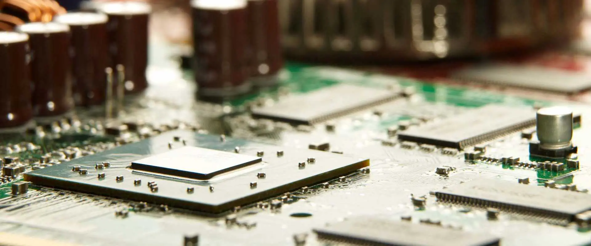
A 7 layer PCB is a more advanced type of multilayer board. This board comprises 7 copper layers. These layers include power planes, ground planes, and routing layers. A 7 layer PCB is ideal for high-speed applications since they include more routing layers.
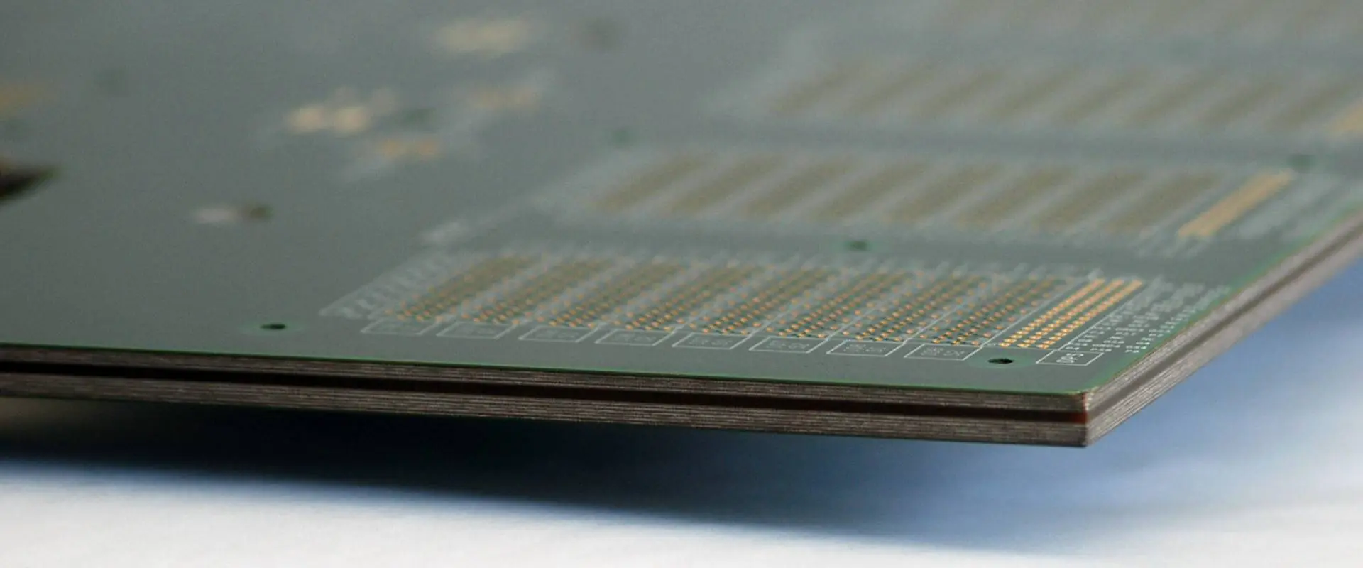
Also, manufacturers use copper-plated holes to interconnect all the layers in this PCB. A 7 layer PCB is complex by design. The top and bottom layers appear as dual PCB. However, there are stacked layers on the two sides of the core. Manufacturers compress all the layers to create a 7 layer PCB.
In a 7 layer PCB, manufacturers assemble the active and passive components on top and bottom layers. The inner layers are for routing. Furthermore, a 7 layer PCB has a top layer, inner layers, and a bottom layer. The thickness of a multilayer board increases as the number of layers increases.
The 7 layer PCB stackup is the arrangement of copper layers and insulators on a PCB. Before designing the final layout of a PCB, manufacturers must create a stackup. It is very important to manage a good 7 layer PCB stackup. A multilayer board is specifically designed to offer solutions to certain problems.
A 7 layer stackup can help to reduce the PCB vulnerability to the external nose. Also, a good stackup can increase efficiency. Good layering can also minimize the board’s impedance and crosstalk. The 7 layer stackup configuration requires proper planning. A poorly designed stackup can increase EMI and crosstalk in a board.
Copper planes in a 7 layer stackup enable signals to route in microstrip or stripline. The function of planes in this stackup is to reduce radiated emissions. A 7 layer stackup comprises signal layers, power planes, and ground planes. In addition, it is important that the signal layer is adjacent to a plane. This helps to reduce the number of signal layers between planes.
Also, manufacturers should couple signal layers tightly to their adjacent planes. In a 7 layer PCB, a power plane can serve as a return path of the signal. Manufacturers add one more plane to the six layer stackup. This helps to improve EMC performance in a 7 layer stackup.
Furthermore, in a 7 layer PCB stackup, a prepreg layer functions as a dielectric between layers. Manufacturers apply pressure and heat to the whole stackup and melt the core and prepreg. This will help the layers to bond well. A 7 layer PCB features more copper layers and dielectrics.
Design Rules for a 7 Layer PCB
There are rules you need to follow when designing a 7 layer PCB. To achieve a functional board, it is very important you pay attention to some things. Here are a few design rules:
Route high-speed signals on intermediated layers. Ground planes can protect and tolerate the radiation coming from the tracks.
Ensure you place signal layers very close to each other.
It is better to use more ground plane boards since they enable signal routing
The mass and power planes must couple rigorously.
Ensure the insulation between a signal layer and adjacent plane is thinner.
Use multiple ground planes. They reduce the ground impedance of a board. Also, they minimize radiation.
A 7 layer PCB is widely used in different applications. This multilayer PCB is well-suited for high-end applications.
Telecommunication electronics
You will find a 7 layer PCB in several telecommunication devices. They are available in radar electronics, satellite, GPS, and more. Also, most of these devices require high signal transmissions. A 7 layer PCB reduces crosstalk and EMI. Therefore, it is ideal for use in such devices.
Computer systems
A 7 layer PCB is available in computer systems. You will find them in graphic cards, motherboards, and other computer systems.
These are electronic devices commonly used in the household. Also, they are important for our daily lives. They include TV remote, smart watches, and more. Due to the complexity of some devices, manufacturers prefer to use this PCB.
Industrial electronics
Electronic devices in industrial systems feature 7 layer PCB. Industrial electronics are different from consumer electronics. Also, these electronics work in harsh environments. Industrial electronics like automated assembly lines and packaging conveyors feature 7 layer PCB.
A 7 layer PCB comprises signal layers, ground planes, and power planes. The signal layers are always used as the top and bottom layer.
Creating the inner layer core is the first step in the 7 layer PCB. This process starts by choosing a laminate that meets the required thickness of the board.
Choose the right materials for prepreg sheets, copper (Cu) foil, and inner layer core. The prepreg sheets comprise glass cloth reinforced with epoxy resin.
Cover the core sheet laminates with copper (Cu) foils. You need to bond the copper to the core material to create the inner layer laminate.
Cover the laminates with photosensitive dry films. This enables the UV light to have contact with the resist.
The internal layers are stacked with prepreg for alignment.
Cover the bottom and top prepreg layers with copper foil.
The next step involves heating the whole unit and fusing the layers in the circuit board.
Drill holes in the circuit board and apply copper on the drilled holes.
After this, add bottom and top circuitry. Cover and plate the circuitry with tin.
Etch away the extra copper and remove the tin. You can now apply a solder mask.
The last stage is testing the board for good performance.
Conclusion
A 7 layer PCB is ideal for use in some applications. This PCB adds to the performance of electronic devices. Also, they help to enhance signal transmission in high-frequency applications.
The PCB interface has long been a challenge. An electronic system must endure an operational temperature range of -55 to 155 degrees Celsius. Alternatively, in extreme cases, it should withstand 250 degrees. So, they need a design with high thermal conductivity.
High thermal conductivity usually means high specific heat capacity and low thermal resistance. They are the two most fundamental properties for designing thermally conductive materials. For example, copper has high thermal conductivity and specific heat capacity. The thermal resistance of copper is relatively low. Thermal conductivity and specific heat capacity are both based on the units of kg/m.K (kilograms per meter per degree). Materials with the same weight have the same thermal conductivity. Unless they have different specific heat capacities, it means their thermal resistances will differ. All else being equal, materials with higher specific heat capacities will have lower thermal resistance than those with lower values.
We use various laminate cores with high thermal conductivity materials to develop very efficient and cost-effective PCBs. In addition, RayMing PCB and Assembly is developing many new laminates to achieve the required thermal performance that the varying markets need.
Mechanically Unsupported, High Thermal Conductivity Laminates RF-60TC PCB is a family of high thermal conductivity laminates that provide 3 to 5 times the thermal conductivity of FR-4 based alternatives.
You need to store the RF-60TC laminates flat in a clean, dry place. Avoid arcing or static discharge.
At temperatures below -40 degrees F, you should protect the laminate from direct exposure to moisture and store it in a dry environment.
Manufacturers anneal the High Thermal Conductivity Laminates Taconic RF-60TC PCB after manufacturing. This means heating the laminate to approximately 200 degrees Celsius, cooling, and reheating over an oven.
Shelf Life
Shelf life for the laminates is five years, but it can last over ten years, depending on the type and application. For example, use in blast furnace applications will have a shorter shelf life than those used in telecommunications.
REPAIR AND REUSING
The laminate color depends upon the processing and the age of the laminate and environmental conditions. The color of RF-60TC laminates resembles that of gold leaf. The laminates may appear to change color as they age. There is no need for concern with this color change.
You can repair or reuse the RF-60TC laminates in most cases. However, you must remove the laminate defects to make an area usable. A common practice is to cut the laminate with a bandsaw such that the damage does not exceed 8mm (3/8”).
HANDLING
PTFE is a thermoplastic material that one can reuse. PTFE is slippery. Handling PTFE requires care not to drop or scratch the material. Passive smoke particles may collect on the surface of the material over time, which will make it look darker but will not impact performance. It is stable electrically and chemically and will not contaminate other materials or cause any adverse effects. RF-60TC laminates are excellent for PTFE substrates as a substrate or top cover.
Avoid mechanical scrubbing, brushing, or sanding
Use a lint-free cloth to dust the laminate surface. Avoid using abrasive cleaners on these laminates as they are very hard-wearing. In addition, stainless steel wool may break at temperatures below 125°C (257°F) and release silica dust that can cause allergic reactions.
Suppose the laminate surface becomes contaminated with a solvent that you cannot remove mechanically. In that case, you can heat the laminate to 175°C (347°F) for a short period. This will evaporate the solvent and recover most of the strength.
It is possible to remove the solder mask from FR-4 PCBs by placing PTFE in water at 60 degrees Celsius (140 degrees Fahrenheit) for over two hours. You can then remove the solder mask mechanically with a pair of tweezers.
Do not pick up a panel horizontally by one end or edge
To inspect the laminate surface, moisten a lint-free cloth with water and hold it in such a way that light shines through but is not visible from all sides. You can obtain the best result with a magnifying glass. If you are curious about the condition of your laminates, you can also use a magnifying glass to inspect them.
It is important to note that a glossy gold or silvery coating on the laminate surface comes from an added metal layer over the material.
Prevent contaminant deposits on the material or copper
Keep the laminates clean during fabrication and assembly. Be careful not to contaminate the surfaces with fingerprints and other soils. They could cause oxidation of the copper or staining of the laminate.
Do not stack panels directly on top of each other
Adherence between the laminate surface and the PCB or PCB substrate is essential. This ensures the excellent performance of the printed circuit. Use a contact material between the PCB substrate and the laminate surface. The contact material must maintain its adhesion over a long period without damage.
INNER LAYER PREPARATION
Taconic recommends connecting the inner layer(s) of the PCB with lands and a power plane. If the inner layer(s) have no connection, vias should connect them to the outer layers.
Acclimation:
The laminate temperature depends on the temperature at which the manufacturers use. Therefore, the surface of the laminates may feel colder or warmer than normal.
The outside layer of most laminate sheets is between 55 and 80 degrees Celsius. At the same time, the glass transition temperature of the core material is between 176 and 205 degrees Celsius.
Scaling:
The thickness of the lamination will relax because of several factors. Reduced cooling will reduce thermal conductivity by 10% from the rated value. Short-term humidity and temperature changes can also affect thermal conductivity. This causes the laminate to have a more abrupt temperature change at one location than another.
LAMINATION
Lamination of the PCB is when you apply a plastic film over a copper clad board to insulate it from temperature, moisture, and vibration changes. The most popular laminate form used today is polyimide with glass fibers. We use other materials for special applications, such as holding metal plating sheets and substrates. Glass fiber laminates are also excellent for separation layers for printed circuit boards.
Flow Patterns / Thieving:
Lamination will have flow patterns different from the ideal planar flow pattern. This occurs because of the lack of proper operation of the laminating machine. Poor adhesion will also cause the feathering of the lamination.
Padding and Conformance Materials:
The laminating process will allow some air trapped on the laminate with gaps between the laminate and the board substrate. Air in this area will cause a decrease in the efficiency of the laminate.
Pressure:
Small cracks may form after removing the laminate’s stress. Therefore, you should not stuff the laminated board with pressure or press it onto it for several minutes after laminating it.
Temperature:
The outer-most layer will have a different thermal conductivity than the core material. This is because the temperature of the outer-most layer has varied during processing.
It is a necessary process that allows for the population of the board with components. Drilling is also used to allow vias between layers and remove material from around features like pin headers and mounting holes. Glass fiber reinforced laminates have excellent drill strength.
Drill Bits:
Polyimide is harder than copper, so that the bit will dull more easily. The composition of the polymer layer may also affect the lifespan of the bit. In addition, the material may have a greater coefficient of thermal expansion than copper. As a result, it will cause durability problems when drilling into polyimide.
Chip Load:
Chip load on the drill bit will affect how quickly it will wear. A high chip load helps generate friction and heat, which may cause the drill bit too dull quickly. You may also scratch the laminate surface, which is especially important for a solder mask that is only 100microns thick. When dull, the bit will also leave rough edges after drilling.
Cutting Speed:
The cutting speed of the drill bit will affect how quickly it will wear. For small hole sizes, a high cutting speed worsens the situation. A lower cutting speed is better for large holes because it diminishes plastic shavings from forming.
Dwell Time:
After drilling a hole, you will have to re-enter the drill bit in the hole. Drill bits that have gotten dull will make this harder. The material may also spoil due to the thermal shock from thermal cycling.
Peck Drilling:
Drilling will generate heat. The polyimide and glass fibers will also generate heat. The thermal expansion and conductivity of the materials will cause thermal cycling. It causes the hole to become oval-shaped and may lead to cracking.
PLATING
The most common plating process is tin deposition, where you deposit a thin layer of the tin onto the surface of the PCB. For solder masks and thin layers of copper, the plating will cause damage to the PCB. Therefore, you should avoid thinner layers. Otherwise, post-plating cleaning may become hazardous.
Metal:
The surface of the copper-clad board does not have to be 100% pure copper. Larger amounts of lead or other metals may cause corrosion problems for electrical connections. The surface may also become pitted after electroplating, especially if there is a large difference in the plating thickness.
Tin Thickness and Coverage:
It is essential to know whether the plating system used will build up in on all areas of the PCB. For example, copper-clad boards with wider than 0.1mm features may have full tin coverage over some areas while having no tin coverage over other areas.
Base Material:
Use the glass fiber reinforced laminates for plating. They are more conductive than their PVC counterparts and do not have the same problems with cutting.
Drill Thickness:
If the drilling process is too aggressive, it may cause damage to the PCB.
Overflow:
The plating tank may not adjust its acid levels, which will cause the plating to overflow onto the board.
SOLDER MASK
Solder mask is a photo-sensitive polyimide film applied to the PCB before placing the components. The solder mask will protect the areas of copper and prevent the solder from flowing there. In addition, the solder mask is dielectric, so the solder will not stick to it. This is important because if solder masks cover the surface of vias and other features such.
After soldering, you will expose the mask to a light source. The polyimide will convert to its original composition. A chemical reaction will occur between the polyimide and the exposed solder. The polyimide will decompose and oxidize in a process referred to as “exposure.” Paste-down:
Conclusion
Lab testing confirms that the High Thermal Conductivity Laminates and High Thermal Conductivity Boards are very efficient in dissipating heat. It allows for an excellent performance of the PCB in a range of applications. This family of laminates will revolutionize PCB thermal performance at Taconic. In addition, it will provide new opportunities for design engineers seeking high-performance laminates.
Electronic devices usually find it difficult to carry high currents. However, with 6oz PCB, you will get a good solution and answer to the problem. With 6oz PCB, you will get the ideal copper thickness to serve any PCB application requiring maximum current.
We believe that after reading this article, you will understand the best possible thickness for the surface of your PCB. Let’s begin.
6oz PCB: What is this?
6 oz copper PCB has to do with a thick printed circuit board that has 6 oz (about 170-09 gm) of copper present in 1 sq ft area of the layer of the surface. This is approximately a thickness of about 8.22 mils.
This PCB is worthwhile because it carries a higher load of current. This low dielectric constant, high temperature for decomposition, and an effective cost will enhance its use in different PCB projects.
Copper thickness helps in promoting the device’s functionality via a surface that is much flatter. This means that 6 oz pcb is a very great option for PCB applications requiring high volume.
6oz pcb features some great dielectric materials. The dielectric materials offer some flexibility in the devices. All these materials offer enough dielectric strength, which helps in Let us consider these materials
CFM
This is called composite epoxy materials. This has to do with a blend of phenol, epoxy, and glass. You apply these materials in through hole technology and surface mount technology of the 6oz PCB.
This fiberglass and resin combined together. With resin, 6 oz PCB will offer impedance stability. Also, it maintains a halogen-free nature.
Fire Retardant
6 oz copper PCB features different materials for fire retarding like FR4. FR4 is seen in glass-based epoxy materials. It offers great glass transition temperature. This plays a vital role in the thermal management of any PCB application.
Once again, the PCB materials feature low harmful halogens. Asides from that, it is lead-free. The dielectric materials (FR1 and FR2) are usually phenol and paper compounds.
Is 6oz PCB Better when Compared to the Standard?
Compared to the standard thickness of printed circuit boards, its clear that 6 oz copper PCB has more superiority. These can be seen from different angles.
More efficiency in transferring the high current in contrast to standard PCBs
The thickness of the 6oz PCB offers a better and more effective mechanical strength against any external forces in contrast to the thicknesses of standard PCBs.
6 oz copper PCB has a very impressive heat conduction, which is higher compared to the standard type.
With 6oz PCB, it is more convenient to place your components in contrast to the standard type. However, standard PCBs don’t offer enough flat surfaces for the efficient placement of components of your printed circuit boards.
This thickness helps in enhancing the impedance of layers of printed circuit boards. Standard PCBs on the other hand cannot enhance the resistance found between the layers.
Best Technologies for the Component Mounting of 6oz PCB
To mount the components of your 6oz PCB, you can make use of the through-hole technology and surface mount technology.
For this, you place the PCB components lead into a hole found on the surface of the PCB. Mounting 6oz PCB with this technology comes at a high price. Also, this mounting technology has a more complicated process compared to surface mounting.
This technology is useful for any tiny PCB component. Here, you place the components on the pad via soldering. This ensures permanent and smooth electrical joints among the components of your PCB. This technology works great for very fast data transmissions.
Design Techniques of 6oz PCB
Before going ahead to design the 6oz copper PCB, there are some factors to consider. These include minimum spacing, dimensions, type, etc. Below are some design techniques you should work with for 6 oz copper PCB.
Levels of copper fill with resin materials ought to be above 75%. If this is not so, delamination occurs.
Make use of more copper when doing galvanic coating
The least spacing required for a copper foil of 105 m thickness must be 13 mils
The solder resists layer thickness has to have at least 0.25 mm
The pathway requires a minimum of 12 mils
A perfect design ensures that the electric circuit undergoes little thermal stress. This is one reason why you must take a look at these techniques before you go ahead to design your 6oz pcb.
With 6oz PCBs, you can be sure that the placement of the component on the surface via soldering is stable. This is why you must fabricate it with care. PCB fabrication includes etching and plating.
You must cover that copper surface area you desire with any photopolymer. This serves as a form of protective layer. After this, keep the PCB in ferric chloride solution. This is to ensure that etching takes place. This solution gets rid of any bare portion of the 6 oz copper PCB.
With etching, there is a reduction in the circuit’s path width via an undercutting effect. During this process of fabrication, you cannot apply any electrostatic spray. Fill the substrate of the 6oz PCB by making use of a solder mask, after which you should apply the solder resist.
This process will surely affect the PCB’s efficiency. With the right fabrication, the 6 oz copper PCB will ensure that it works well with high-power tasks and projects.
What Type of Surface Finish Process Works Best for 6oz PCB?
ENIG finish serves as the most effective finish. This ensures that the efficiency of the copper PCB is promoted to a large extent. Also, ENIG improves the 6 oz copper PCB’s lead-free compatibility. This also helps in widening the surface of the PCB, which promotes the component placement’s productivity. You can design the PCB’s solder joints easily.
Furthermore, ENIG helps in resisting the surface of the PCB from corrosion. This gives the device more longevity.
Conclusion
6oz PCB is a trustworthy option to improve the performance of your device. With this, you’ll get the best possible output of your electric circuits. With the different benefits of the 6 oz copper PCB, you will surely design your superlative projects with ease.
The digital age is upon us, as is the need to produce increasingly robust and reliable products. That’s where manufacturers like Taconic come in. Their manufacturing facilities offer you several solutions for your product requirements. Also, the accompanying demands that go with such sophistication.
It is necessary to look at some essential features before we can stop talking about the various ways in which Taconic materials are crucial. This will not only help you when it comes to choosing the best product for your needs. But it will also inform us about its various capabilities.
Taconic materials are exceptional in many ways. One of the most critical aspects of such materials is their high degree of strength. It is why they are available in several different forms. Taconic is famous for its products based on polyurethane resin. We use it to create durable and reliable products that hold up well under intensive usage conditions.
Another essential element for Taconic materials is their resistance to damage. Besides being strong, they can also resist various types of wear and tear. It means that they remain functional even if we expose them to extreme conditions. This means that there is no need for you to spend extra money on more repairs and maintenance later.
The NF-30 ceramic composite material is one of the most popular and dependable products that Taconic offers. It is available in many different forms, and it is incredibly robust as well. Its ceramic fibers embedded within the material make it exceptionally resistant to wear and tear. It means that you can use it for a long time without worrying about its durability. This will save you money, as you will not have to spend additional funds on repairs and maintenance later.
We need to store NF-30 laminates flat when not in use. The NF-30 series offers exceptional resistance to impact and abrasion. It is another essential feature for any product you want to buy. So, you should look for products that exhibit excellent longevity and resistance to wear and tear. This will ensure that you can use the material for a long time. It will help reduce spending on repairs and maintenance later.
Another essential feature that you can find in the NF-30 ceramic composite material is its ability to resist heat and cold. When we expose the products to extreme conditions, we must treat them with various types of protection. This makes them more attractive to manufacturers, as they can access a wider range of customers who need their services.
How to handle the Taconic NF-30 PCB
NF-30 laminates are without a woven glass fiber binder. This means that once they are in their state, you can handle them without fear of breaking into smaller pieces.
A customer should handle rather than handle Taconic laminates with care.
NF-30 laminates are generally easier to handle and process than most similar materials. But this depends significantly on the individual product you are working with. It is always good for manufacturers to work with individuals who experience the product when using it. This makes it easier to tailor the material to meet your specific needs while ensuring that you can always get the most out of it.
When it comes to handling materials, one of the most important aspects is ensuring that you do not damage them in any way. The NF-30 ceramic composite materials are relatively easy to handle if you take care of them.
Taconic NF-30 copper PCB
The copper NF-30 is a low thermal conductivity material. It is not suitable for heat transfer applications. It is therefore not at all ideal for this type of application. This makes it a very poor choice from a manufacturing point of view.
NF-30 copper laminates will have some crystallization defects on board near the edges. It will also have connector failures. These are also possible due to thermal shock during processing or transport.
NF-30 copper laminates (if rounded) will deteriorate uniformity at the edges and corners. If rounded, they may also have internal defects and pins breaking off.
We can use NF-30 copper laminates for panel mounting only. The process is not suitable for pelletizing.
Another factor that we often overlook is their resistance to heat and cold and their very high durability. A highly durable material used in heat transfer applications can be a desirable option for some clients, as it will save them money in the long term.
Taconic NF-30 aluminum PCB
NF-30 aluminum laminates are not suitable for this type of application.
NF-30 Aluminum laminates have limited-service life. They will have tape distortion, peel apart of laminate edge, and water droplets on the surface when cupped.
We can use NF-30 Aluminum laminates for panel mounting but not for other applications. The process is not suitable for pelletizing.
Besides the fact that the Taconic materials are heat resistant, they are also very resistant to corrosion and wear and tear. This makes them a very versatile material that you can use for different purposes, depending on the application at hand. It is often good to use these materials for heat resistance applications.
Properties
Taconic offers many different types of composite materials suitable for various applications. The NF-30 series can offer exceptional mechanical and thermal properties in heat resistance. The material can maintain its excellent physical and chemical properties. It does this even when exposed to various abrasive and corrosive wear. This means it is a trendy choice in the manufacturing world.
These materials are very versatile, meaning that we can use them as a mat or pad, as well as a molded or expanded piece. However, it can be challenging to work with this material without the correct manufacturing production line. Manufacturers must ensure that they look for a company like RayMing PCB and Assembly with extensive experience working with NF-30 composites.
This type of material is also resistant to heat, meaning that it is durable and can survive many types of wear and tear. But it is a desirable option for those looking for a durable material for their manufacturing line. It will ensure that it lasts for an extremely long time.
Benefits of using Taconic NF-30 PCB
1. Non-reinforced laminate
NF-30 laminate is an accurate, flexible material. So, it does not need internal reinforcements to produce a stable and rigid finished product. As such, it is possible to produce PCBs that are very lightweight and, at the same time, very durable. In the end, this saves the customer money in the long term.
2. Exceptional low electrical loss for microwave applications
The NF-30 is a pure ceramic material, making it very insulating. Consequently, it can offer outstanding electrical resistance in microwave applications. This means that it will be challenging for customers to pick up radio signals and signals on their radio.
3. Excellent adhesion to Very Low Profile copper foils
Taconic materials are among the most flexible materials used for PCB production. They are extremely strong, so it is also possible to use them for various applications where strength is not essential.
4. Stable dielectric properties vs. temperature & frequency
The Taconic materials are much more heat resistant than standard PCBs. They also have very stable dielectric properties. They do even when exposed to higher temperatures and frequencies. This means they are a very popular option for various heat transfer applications. They work best in the aerospace industry.
5. Dimensionally stable for multilayer applications
The Taconic materials are among the most stable materials used in multilayer applications. They are beneficial for RFID applications, especially for devices like cards and tags.
Taconic makes various products used in the aerospace industry. They include electronic parts and heat shields. We use these specialized composites in the manufacturing process of various products. They include radomes, sensors, antennas, and even components. The non-reinforced laminates are especially useful for lightweight yet durable applications. Taconic has even developed a unique metal particle system for this material that we can use to produce such components. This is a significant improvement because it makes the manufacturing process even less expensive.
We often use this type of material in passive components. Passive components are small and cheap RFID tags. We need them to be lightweight, reliable, and resistant to wear and tear. As a result, Taconic’s non-reinforced materials are a popular choice for passive components.
3. Global Positioning System Antennas (GPS)
Taconic materials’ heat resistance and high resistivity are instrumental in GPS. So, we use the materials to produce the antennas in this system. It ensures that the product will outperform many of its competitors. This is a critical component of any GPS product because the antenna makes sure that different satellites can pick up the signal.
4. Automotive Radar Sensors
We also use Taconic materials to produce the radar sensors found in cars and trucks. Most radar sensors use thermal imaging, an essential part of radar technology. As such, the Taconic materials are beneficial in these applications. We also use them in applications where we need RFID components. Some examples include parking sensors and license plate readers.
Remote Contravening Elements are essential in various industries and fields. They include many sectors within the automotive industry. As a result, Taconic materials have become very popular in this field. We use them as countersinks and surface shapes on instrumentation modules. It is necessary to ensure that we can integrate the components with other electronics systems without problems.
Conclusion
When choosing a material for your manufacturing processes, you will find that numerous factors can make or break the process. Therefore, it is so important to look for a high-quality provider. They should have a great deal of experience and expertise in the field. You should consider various materials before making your final decision.
Taconic NF-30 PCB materials are an exceptional choice for several applications. It can also cause many problems for your manufacturing line when misused. Make sure that you choose the correct materials. After several different options, you should find the perfect item to work with.
In the past, designing a PCB board meant that you would have to purchase expensive CAD tools from a single company that could cost thousands of dollars for an annual subscription. However, as the industry has grown over the last decade, multiple options are available to engineers and hobbyists alike. Nowadays, some people recommend Altium – whereas others prefer Kicad – but it can be challenging to know which one is best for you and your needs.
The good news is that both programs are entirely free to use. Kicad offers a 100% open-source design platform that allows you to use any brand of components in your projects. On the other hand, Altium is entirely proprietary and tightly controlled by its parent company. They do not allow you to use open-source components or share your designs with others. These programs are available for Windows and Mac computers. They get frequent updates (sometimes on different schedules).
So, the first thing to consider when choosing a design program is whether you need a schematic editor or a PCB layout program. Schematics are the blueprints of your electronics and cover voltage, current, and other measurements. However, they are also helpful. They allow you to connect components like resistors, transistors, diodes, and integrated circuits into a circuit board. PCB layouts specifically refer to the physical layout of a PCB board. Each of these programs has its strength in schematics or PCB layouts.
To help you decide which one is best for you, it is essential to know what each program can do.
Before we begin, it’s essential to keep in mind that PCB design is a particular field that requires expertise and knowledge. While these are for beginners, they contain valuable information on easing into the process.
Kicad has been around for several years before Altium. It was initially created in 2003 by Jean-Pierre Charras and is available for Windows, Linux, and Mac. Back then, the company’s main goal was to provide a user-friendly interface for hobbyists who wanted to design a board without paying thousands of dollars for a single program.
Both Kicad and Altium depend on the open-source community to help improve programs and provide support when there are issues. Therefore, upon initial installation, you must install several other programs for Kicad to function properly. The installation process can take anywhere from three to six hours, depending on your system.
However, it’s well worth the time because it has many powerful features. They include customizable drill sizes for different board materials. These materials are very helpful when dealing with small-scale PCB design tasks. Furthermore, this tool is open-source, so it’s free for private and commercial use.
Grading Criteria
It’s important to note that all the following criteria depend on a scale of 1 to 5. One is the worst, and five is the best. There is no single “best” program out there. It varies from user to user, depending on your requirements.
Usability
As far as usability goes, PCB design – especially for beginners- is worth noting. It can be challenging because it requires patience and practice to become adept at using the tools. Therefore, it’s essential to keep this in mind and make sure that you understand the process before making any significant decisions.
Kicad has a very straight forward layout that’s easy to understand and even includes “preview” mode. It allows you to see how a design will look once you print it. However, it is essential to note that several people have said some errors in the PCB design process due to Kicad being open source.
Furthermore, it’s important to note that Kicad is incompatible with Windows 10. Therefore, if you have upgraded from Windows 7 or 8.1 to Microsoft’s latest operating system, then you will have to run an older version of Windows for the program to run correctly.
Numerous components are available (more than 55,000)
Can automatically create a netlist based on the design in Eagle.
Cons :
Poor documentation, although we expect this since it is open-source software and “user-specific.” It cannot align nets like other PCB design programs. It uses a BSD license, so it cannot create commercial designs that use the original code. Limited Gerber viewer – cannot view traces, pads, drill holes, etc. Can export files in DXF format (Altium does not offer this option)
We should purchase programs like Kicad for the experience of using a complete open-source apparatus. In other words, you purchase the tool and become the owner/developer of it instead of purchasing a service from a giant company that has adequate training but does not make you an active part of its community.
What do Kicad and Altium Offer?
Both Altium and Kicad are pieces of software that allow you to create PCB boards. With both programs, you can easily lay out your circuit design and flow it from your schematic to the printed board itself with little trouble.
But the benefits of Kicad tend to be more focused on its open-source nature. You can use anything compatible with Eagle, such as Altium brand electronics and sensors.
On the other hand, Altium also offers a suite of machine components compatible with Eagle right out of the box. However, these ‘generic’ parts tend to be more expensive than their Altium counterparts.
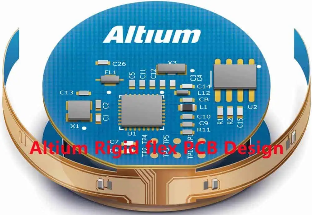
Kicad rigid flex
Companies often tout Kicad rigid flex PCB design as a cost-effective method to produce your PCB. This is because, if you are only designing prototypes and small batches of products, using Kicad rigid flex and hand assembly can be very convenient and inexpensive in the short term. However, Kicad rigid flex PCB is not without its disadvantages. One of the main drawbacks of this design method is that you cannot use the software to generate Gerber files and print your board. If you want to create boards using Kicad flex PCB, you must obtain a PCB maker to manufacture your prototype boards professionally. Fortunately, it is possible to purchase Kicad rigid flexArduino shields to access all the features included with their paid version.
Manufacturing PCBs using Kicad flexible PCB is also time-consuming, challenging for the impatient. On average, it will take you around two to eight hours to complete a design using Kicad rigid flex – depending on how familiar you are with the software. Using this method also requires patience when uploading designs to your computer. You may need to wait anywhere between fifteen minutes and six hours for the board files to finish uploading before you can test them.
As far as the basic ‘package’ goes, Altium offers three different options for new users. However, it’s important to note that each package has varying costs attached. The most basic package costs $200 per year – and they can only create a handful of boards. On top of this, most Altium users will find that they don’t need to purchase the newest parts in the package – but that their designs will still be available in their library.
For a nominal annual fee ($120), you can use all Altium’s tools and parts. However, this option comes with a decreasing amount of content for each board. For instance, the number of parts and files diminishes.
The next package up is the Professional package. This cost is $500 per year but comes with over 90 components included in the design library. Additionally, one can easily make each board work on multiple rigid flex PCB altium thicknesses – medium and thick.
Finally, the most expensive package is Altium Designer. This costs $600 per year. It contains over 600 parts and access to all the latest components from Altium. It also comes with a fully-featured editor, which makes it possible to modify designs and layouts continually – if you so choose.
Flex And Rigid-Flex Design Challenges
It is possible to design both rigid and flexible PCBs using Kicad’s rigid flex method. However, even though you might create a circuit using the rigid flex method, you may find that they are difficult to solder and assemble.
On the other hand, it can be challenging to get anything to stick together when creating PCB boards with Altium flex rigid toolset. The parts and connectors tend to be a bit too tight together when manually laying out your designs. This can make it difficult for components to align and the board to fit in properly.
Kicad’s rigid flex, on the other hand, is one of the easiest ways to get started with PCB prototyping, whether you are a CAD user or not. Since all electronics and components integrate into one software platform, you can ensure that your designs will work.
On the other hand, Altium’s rigid-flex toolset does not have the consistent functionality that we find with Kicad. In addition to this, it is difficult for you to lay out the board yourself – since you will need to purchase a PCB maker to produce your boards.
Altium Designer vs. Kicad
Altium Designer is the most expensive, professional-level package. Kicad offers a simple installation process and easy usage of its system. We can send each design directly to the manufacturer for fabrication online – without any interaction from your end. So, Kicad’s installation process is a little bit trickier than Altium’s.
Additionally, while small, Kicad’s community is still an excellent resource for new users to learn more about their software. Because Kicad is open-source and free to use, its forums are always full of eager learners. Altium’s forums, on the other hand, haven’t received updates very often in recent months – which can be a bit of a challenge for new users.
In this sense, the main difference between Altium and Kicad lies in the community behind them.
Advantages of using Kicad
1. One of the most significant advantages of using Kicad is that all parts and components integrate into their system. This means that it’s very easy for anyone to start creating a PCB design without purchasing any expensive tools or machines.
2. Kicad is also user-friendly, so new users will have no problems getting started with their designs. In this sense, it’s easier to learn how to use Kicad than Altium designer.
3. Kicad also offers many parts – from essential components like resistors, capacitors, and transistors to more sophisticated ICs and sensors. This makes it very easy for engineers to fabricate prototypes using the latest technologies in electronics.
4. Kicad also has a very affordable cost structure for users looking to start circuit boards quickly.
5. Finally, you can use Kicad online to create your designs without the need for a computer. This allows you to create your PCB designs and upload them directly to their manufacturer for fabrication.
Disadvantages of using Kicad
1. It is somewhat difficult to lay out the design on the screen in a way that accurately represents what your final product will look like when you manufacture it on a board.
2. Some Altium users have complained that they find it challenging to use Kicad online, particularly when multiple designers are working on one project simultaneously.
3. In addition to this, it is challenging to add components and parts to your designs in a way that will look aesthetically pleasing. This can be tricky for new users who are still learning to work with their designs and layouts.
4. Finally, it isn’t easy to get a circuit diagram to look as clean using Kicad as it does in Altium designer. However, both Altium and Kicad offer users the ability to test-run their designs before sending them for fabrication. It is a true advantage for engineers who are not very experienced with PCB design software.
Advantages of Altium
1. Altium is a high-quality, professional-level PCB design software that comes with all the bells and whistles you would expect from a top-of-the-line program.
2. We can use Altium to create everything from nothing with their circuit maker to more complex designs using the freely available library of components. This makes the toolset very versatile and accessible for many electronics engineers.
3. Altium also offers an array of tutorials and other documentation that will help you improve your design. This means that it is easy for even the most novice users to learn how to use the software and get started with their designs.
4. Its online community is also beneficial for new users, who can ask questions about the software if they need assistance. Since it centers around the same principles as other microcontroller programming languages like Arduino, it is easier for new users to study and understand how the program works.
5. Finally, Altium rigid flex toolset is one of the most advanced software platforms on the market today. The flexible board used to build circuits is easy to assemble and solder. It makes it a perfect choice for engineers who are just getting started with PCB design tools.
Disadvantages of using Altium
1. Altium can be expensive for new users, especially since it does not have a free trial version because Altium offers so many features that their license fees are higher than Kicad’s.
2. We can also use online like Kicad – which means that users will need a computer to learn how to use the toolset properly.
3. However, we offset this by the availability of additional documentation and help within their community forums and reports on the toolset.
4. It may be more difficult for new users to use Altium without the available training materials. Especially for those still learning about the programs and the structure of rigid flex PCB altium design software in general.
How to use Kicad to create rigid flex
You should know that there are two ways to create a circuit – rigid and flexible. Rigid flex PCBs have the rigidity of a typical PC board, and we can manufacture it using any fabrication process. Flexible PCBs have the flexibility of a wire, and companies manufacture them using selective metal stamping processes that use metal powder as a mold rather than inkjet printing. This process allows you to easily design your circuit with readily available blank PCBs in plastic or FR-4 material.
This process includes:
1. To start creating a PCB using Kicad, you must first sign up for a free account. Then, you need to download the Kicad software.
2. Once you have downloaded the software, you will want to open the starter kit. This is the file included with your copy of the program when you purchase it online.
3. The starter kit file will contain all the necessary parts to create your PCB. However, you will still want to download your free Kicad library. This file contains all the parts and components that you can use when designing a PCB.
4. Once you have downloaded your free components and parts, open up Kicad and create a new blank project.
5. Then, you need to select the correct hardware for your design by navigating to the customize tab and clicking on the board types button located on the left-hand side of the program.
6. A new window will appear, allowing you to select the type of hardware you would like to use for your project.
7. After selecting the right board type, you will want to navigate back to the “customize” tab and click on “library.” This will give you access to your new library and the components and parts included with it.
8. You can then start designing your circuit by attaching several components according to how you want your design to function. After finishing with your design, you can save it and then save it as a PDF file.
9. Finally, you can then upload it to one of the dedicated fabrication sites that are available online. This will allow for a quick turnaround time for your finished PCBs in high-quality PCB material.
Altium Designer is one of the most widely used PCB design software programs on the market today. The program is perfect for electronics engineers and hobbyists who are just getting started with the industry.
1. To start creating a PCB using Altium Designer, you will first want to download the application.
2. Next, it will take you to the software – which will look like a web browser – and allow you to create a new project in seconds.
3. Once you have created a new project, you can customize the board by selecting the correct hardware and components.
4. You can then add a variety of components to your circuit – including resistors, capacitors, transistors, and more.
5. Once you have finished designing your circuit using Altium Designer, you will use the “fabrication” tab to generate the final design file that you need to manufacture your PCBs in a professional facility.
6. After you have finished this step, you can review your design and ensure it is correct before sending it off to the fabrication facility of your choice.
7. After producing and manufacturing, you will receive it in a matter of days. It means that Altium Designer is one of the best choices for anyone who wants to create a flexible PCB at home quickly and easily.
The Future Of PCB Design Software
The future of PCB design software is trying to utilize all the latest technology, mainly in simple operation. Therefore companies like Altium, Kicad, KiCad, and many others are trying to develop something that could be a game-changer. These programs are already something they call “one-click PCB,” where you can design a circuit in one click.
This software is getting more and more user-friendly with the help of big companies. If this trend continues, it is evident that we need future generations to design their circuits at home. These latest developments will allow practical 3D circuit simulation, a more intuitive way to design schematics and other options to make circuit design easy.
These are just some tips that you can use to create your flex PCB. It may seem like these programs can do everything on their own – which is why so many people have started using them in recent years.
The truth is that as we move forward in time and technology, there will be more and more ways for us to design our circuit boards. It is truly amazing how far developments have come. If you plan to create circuit boards at home shortly, you should already be familiar with creating PCBs using these programs.
Conclusion
Both Altium and Kicad are excellent choices for any PCB designer that needs a professional solution. Altium is straightforward to use if you’re looking to recreate a design or plan it out from scratch. They also offer plenty of content in their design library – as well as a wide selection of parts and electronics on their website.
Kicad, on the other hand, is a little bit more complicated. However, they offer so much freedom to their users when modifying their designs. All of Kicad’s changes are open-source and available for everyone to view. If you’re not afraid of coding, then you’ll enjoy using this software. You can rest assured that your designs will always be compatible with the community.
PCB is a resilient non-conductive board put up on coated based structure. The PCBs are mainly used to supply electrical bonds and mechanical aids to a circuit. Also, they are frequent in electronic gadgets, mostly visible as a green-colored board.
The bonding of components found on the board that serves as a pathway to electric signals is through the copper. Active and passive components are firmly mounted on the PCB to meet the form factor of a final design. The form factor is the hardware properties that indicate vital physical properties of a PCB.
To determine the design of a PCB, these form factors are necessary for consideration. PCBs have advanced over time. The advancements experienced in the electronic industry birthed the multilayer PCB. They vary in complexity while the design began from single layer to complex design such as 28 layer PCB.
The growth factor in the electronic industry hinges on the capacity to route electrical signals upended. Vias and surface mount devices enable the smaller size of boards with increased components. The ideal number of layers on a PCB relies on the application needed on the design. Thus, a 28 layer PCB is a design with 28 layers. Also, its space could accommodate the needed number of elements.
A multilayer board has more than 3 layers present in the design. An increase in demand for multilayer was due to the desire of end-users for small complex devices. Also, it is a perfect choice for numerous professional electronic gadgets. The 28 layer PCB consists of numerous laminated layers. It allows for extra circuitry and wiring for composite applications.
The versatility of the multilayer PCB contributed to its growth. As the request increases, so do the number of layers produced increases. Thus, the 28 Layer PCB was specifically produced to meet the demands of composite designs. Applications such as satellite systems, file serve, GPS technology, and many more.
It is crucial to note that the 28 layer PCB could come in a different layout. However, mostly it is a multilayer rigid PCB design. A rigid PCB design comprises solid materials that do not give room for bend or twist of shape. It has a high lifespan, thus it is the preferred option for use in computers like CPU and GPU.
The 28 Layer PCB being a multilayer rigid design is compact. The number of layers involved aids its compactness. These layers help to impede electromagnetic interference produced by the device. It also offers low design and installation costs for the high-volume fabricating task. It is cost-friendly due to the material selection and holes required for the manufacturing process.
Characteristic of the 28 layer PCB
This type of PCB design is being manufactured massively. Its characteristics are valuable to the growth of the electronic industry. The 28 layer PCB is a multilayer design present in devices like the computer motherboard. The following are the characteristics of a rigid multilayer PCB.
The 28 layer PCB is a conventional PCB. It has a flame retardant build-up which increases its rigidity. Also, it maintains a solid shape that can’t fold or twist to any other shape.
It also consists of copper traces and paths integrated into the single board. These copper traces connect various elements on the board. Solid substrate forms the base material of the board. It enhances the board’s strength and rigidity.
It has solid characteristics that imply the design can only maintain a certain shape. Also, it does not allow for any modification or folding.
Another main characteristic of 28 layer PCB is its cost-efficiency. It is cheaper than other types of PCBs. The multilayer PCBs are common in various electronic devices.
It is excellent at connecting multiple electronic elements on the circuit boards.
Components of a 28 layer PCB Stackup
Being a rigid multilayer design, the 28 layer PCB comprises different layers. It has a solid shape from different layers joined by adhesive and heat. To develop such design, the following materials are crucial
Substrate Layer
The substrate layer could also be referred to as the base material. It is made of fiberglass that ensures rigidity and solidity of the board. Epoxies and Phenolics could also serve as the base material. However, they are not as efficient as FR4. They are cheaper with a special lousy smell.
This explains the placement of laminated copper foil on the top of the substrate layer. Applied heat and adhesives aid in the lamination process. Both sides of the board require copper lamination. They could come with varying thicknesses described in ounces per square foot.
The solder mask layer stays above the copper layer. It serves as the insulator on the copper. This helps to avoid damages that could arise from conductive materials.
The silkscreen stands above the solder mask layer. It is the material used to add symbols and characters to the board. These characters and symbols help to understand the board better.
The structure of the board consists of the following:
Through-Hole/Via: Via is an element used to insert components on the board. It makes lines for the connection of more than two layers. However, the non-plating hole is to fix the screw during the assembling process. It is suitable for surface mount positioning.
Marking/Silkscreen: This is an unessential structure. Its primary task is to indicate each part’s name and spot frame on the board. This helps to expedite identification and maintenance after completion.
Dielectric: This material serves as the insulating layer of a 28 layer board. Manufacturers use it to bond the layers of a circuit board. It is also known as copper foil.
Conclusion
A 28 layer PCB comprises different layers of coppers. It is a reliable and functional board. The growing demands of compact devices resulted in the advent of multilayer boards. A 28 layer PCB is a great option for applications that require impedance control. Therefore, this board is well-suited in advanced electronic devices.
Sometimes, the struggle that surrounds choosing an ideal laminate material for your PCB design becomes painstaking. Perhaps, it is best understood by those who have designed printed circuit boards before. For instance, what material can work for PCB applications, yet avoid interfering with your PCB attributes?
Typically, your application area will determine and influence your PCB material choice. Regardless of the application, you must become smarter to ensure a reliable, consistent, and thermally stable PCB. It becomes more critical to design a PCB for a high-power application.
So why not forget about your typical FR4 material for a moment and think outside the box? An excellent alternative in the Taconic TSM-DS3M laminate can work wonders. This article will explore Taconic TSM-DS3M material, its attributes, and how it makes your PCB better for your unique application.
TSM-DS3M comes as a trendsetting and thermally stable low loss core. You can already get the picture when you start considering its Df of 0.0011 at 10GHz. It gets fabricated with consistency and predictability of RF4 (glass-reinforced epoxies). However, TSM-DS3M is a unique ceramic-filled (to reinforce) material with a low fiberglass content – mostly less than 5%. It rivals epoxies mainly in the fabrication of large format complicated multilayers.
A TSM-DS3M PCB by design proves ideal for high power areas of application. In such applications, it becomes necessary to ensure the dielectric material of the PCB conducts the generated heat away from other sources of heat. Therefore, TSM-DS3M has low CTE (coefficients of thermal expansion), especially for exerting thermal cycling.
In most instances, you will find TSM-DS3M combined with a fastRise 27 prepreg. With a Df of 0.0014 at 10 GHz, the material combination proves a perfect solution with the least dielectric losses only comparable to epoxy-like fabrication temperatures of 420-degree Celsius. Further, the characteristic low insertion losses can only compare to fusion bonding – where Teflon laminates get melted within a range of 550 degrees faradays.
Why Avoid Fusion Bonding?
Fusion bonding proves an expensive technique. Besides, it also leads to excessive movement of the material. It would help if you also watched out for the extra stress the movement causes on the plated through-hole. In an instance where you want to design a multilayer, the price or cost of poor yields will increase the ultimate cost of the final product. Therefore, we at RayMing PCB often advise alternative materials and parts like Taconic TSM-DS3M. The fastRise component of the material will allow for the sequential lamination of the product – TSM-DS3M at a paltry 420-degree Fahrenheit.
Important Notes to Consider when Designing Your PCB Using Taconic TSM-DS3M
The intended application should rank the highest in the factors you must consider when designing your PCB using Taconic TSM-DS3M. For instance, if you want to use your printed circuit board for RF or microwave application, then TSM-DS3M can become useful. It will ensure that the vital spaces between traces in couplers and filters have little to no movement with temperature due to the low CTE values of the x, y, and z-axis. Additionally, TSM-DS3M can get deployed with low-profile copper foils, which yield smooth edges on either side of the coupled lines.
If you desire variation and yield in copper weights, you should consider registration over numerous layers. Further, copper etching across the panel at times leads to non-linear movements. Consequently, you may end up with a non-registration of some of the pad’s drilled holes, ultimately leading to open circuits.
TSM-DS3M comes compatible with OhmegaPly and Ticer resistive foils. The resistor foil’s stability comes when you laminate at a low temperature, primarily when using AGC’s fastRise family prepreg. Additionally, TSM-DS3M’s intended application entails RF circuitry and thus needs an original electronic manufacturer design validation when intended for digital circuits.
Taconic TSM-DS3M Product Features
It is dimensionally stable and a laminate with low loss attributes
Has a Dk+ tolerance of 2.94 with a plus or minus margin of 0.05
It has a DF of 0.0011
Low Z-axis expansion
Compatibility with resistive foils
Predictable and consistent attributes during manufacturing
Benefits of a TSM-DS3M
Industry-leading PDF of 0.0011 at 10GHz)
A low Z-axis expansion, especially for military areas of applications
In most cases, the dielectric constant’s thermal coefficient gets abbreviated as T, K. However, the dielectric values from dielectric test approaches depend on the specific approaches. T, K proves similar and will rely on an approach that applies pressure with securing or clamping to eradicate air gaps between the pattern cards and dielectric substrates. Whenever you measure it with a fabricated printed circuit board, variations of circuitry patterns (width and length) can get observed. It explains why the PTFE consistently demonstrates a negative T, K.
Another crucial factor encompasses molecular vibrations or interactions that escalate with temperature. It thus results in an increase in dielectric constant (Dk) with temperature. It is a common occurrence with many epoxy-based laminates. For IPC standard approaches, clamping of the samples under pressure tends to prevent the normal expansion of the laminate in the z-axis. As a result, it may not represent the military or industrial application.
Aspects to Consider for Your Taconic TSM-DS3M Laminate
To design, develop, and use a Taconic TSM-DSM PCB, you must understand some basic aspects of the material. It includes storage, handling, layer preparation, lamination, etc.
Storage
If you want your TSM-DS3 material or laminate to stay perfect, you need to store it flat in a clean area and at room temperature. Additionally, the core gets preserved well when stored between stiffeners. It helps avert any unnecessary layer bending. You can use soft slip sheets to keep debris and dust from embossing into the material. What’s more? The storage conditions determine the shelf-life of the Taconic TSM-DS3M laminate.
Handling
The composition of the TSM-DS3M makes it a unique laminate for Taconic TSM-DS3M PCBs. Because of its properties, it becomes crucial to avoid any mechanical scrubbing. You also have to stop picking up the panel horizontally using either side of the edge or end.
Other handling considerations should entail the prevention of contaminant deposits on the copper or material, avoiding any panel stack up – one on top of the other. It is also crucial to avoid mechanically abrading the PTFE surface post etching.
Layer Preparation
It is crucial to acclimatize and scale when preparing the layers for lamination. However, during the actual lamination, you need to follow the set guidelines to ensure a proper and functioning TSM-DS3M PCB,
Final Thoughts
Taconic TSM-DS3M is an excellent laminate material for high-RF applications. However, while picking it in isolation might appeal to anyone, you have to remember that it works in combination with fastRise prepreg for best results.
The RF-35HTC is a single-sided, thru-hole plated dielectric laminate with a silver (Ag) surface and aluminum oxide ceramic substrate. The Ag surface on the RF-35HTC laminate provides an effective heat dissipation material. At the same time, it maintains low thermal resistance. This combination makes this product suitable for high-power/high-performance applications. You enjoy this where we would require larger heatsink areas without this board. The RF-35HTC has a pre-expanded copper pad on one side to allow for larger pads on the other side of the PCB. Established manufacturers such as RayMing PCB and Assembly plate this product through a single gold (Au) layer, then exposed and plated on both sides with aluminum oxide (Al2O3). The RF-35HTC board is non-metallic, electrically conductive, and is available in many grades from 15 µin (0.058mm) to 4 in (100mm). This laminate is available in both FR and CFR material types.
Copper Layer Information
The Taconic RF-35HTC surface plating combines an oxygen plasma etch and a tin (Sn) electroplating process. The US industrial standard (AIM) specification limits board thickness to less than 500µin via dry film. We should consider the aluminum oxide “cap” on the RF-35HTC laminate part of the overall board thickness for FR and CFR materials. Then we plate the RF-35HTC laminate with an oxygen plasma etch to pass the surface. Afterward, we plate it by an Sn electroplating process, which provides Ag anodes for the Au plating process.
They plate the RF-35HTC laminate with a tin (Sn) electroplating process. This process builds up the Ag (Ag + Sn2+) anode layer by adding another layer of Ag and Sn to the surface. The final Au layer on this laminate does not contain Ag since we anneal it. However, it does provide both electrical conductivity and a barrier against copper oxidation.
This surface is then exposed to a 400 Watt Oven bake at 50C (122F) to evaporate the Sn, leaving behind Ag. They apply a final Au plate over the entire laminate. You cannot directly bond the AU layer to the Ag layer because of the annealing process, so the Au traces and pads must electrically connect it. This Au layer is then exposed to a passive anneal.
This passive anneal softens the Au conductors, allowing them to “flow” into the grain boundaries of the Ag plating. The Au will not enter the Sn grain boundaries as it is incompatible. This flow creates electrical continuity between the Au surface and the underlying Ag plating.
The final step in this process is a second 400WO bake at 50C (122F). This second bake “evapuates” the Au out of the grains.
The RF-35HTC laminate is a dual-sided double conductive epoxy board. They plate both sides with copper via Ag electroplating. You can accomplish this by creating a copper (Cu) layer on one side and the remaining copper epoxy (CE).
We plate the Cu side similarly to the Tin side, with an Ag electroplating process and a 400WO bake.
After creating the Cu layer, we expose it to a dry film deposition (DFD) to reduce its thickness. This reduces surface impedance, spacing, and cost by reducing the thickness of the conductor. The final step in this process is a second 400WO bake at 50C (122F). This second bake “evaputes” the copper out of the grains.
They then expose the CE layer to a 400WO bake. This process evaporates the CE out of the grains, leaving behind Cu. Then we apply a final Au layer over the entire laminate. You cannot directly bond the CU layer to the CE layer since we anneal it. However, it does provide both electrical conductivity and a barrier against copper oxidation.
The conductivity of the RF-35HTC laminate
The Copper Epoxy Layers are non-metallic, electrically conductive, and are available in many grades from 15 µin (0.058mm) to 4 in (100mm). This laminate is available in both FR and CFR material types.
The RF-35HTC laminate is relatively conductive. However, it will not be an ideal board for high-power applications without a highly conductive surface layer. This is because the RF-35HTC laminate does not have the electrical resistance of a conventional PCB (the “R’ term). However, it has an effective resistance of 100Ω or less. This, combined with the high thermal resistance of this laminate, means that heat transfer and dissipation can be slow. They design this material with this in mind.
Impact Resistance of the RF-35HTC Laminate
The laminate composition is not a very good heat transfer compound. Instead, it is primarily an electrical insulator. To become a suitable heat transfer medium, it must have multiple skin effects. It must also have diffusion layers that increase its conductivity and decrease its resistance (the “T’ term). The RF-35HTC has an effective thermal coefficient of expansion (E) of 6.7×10/°C, an absorption coefficient (A) of 1.0×10/Wm, and a dielectric constant (K) of 0.36 to maximize its heat transfer. To increase this thermal expansion coefficient, the laminate consists of non-brittle materials. It has no voids or voids that will cause buckling or void formation when the temperature increases:
The E value for copper is 5.4×10/°C.
People often denote the effective thermal expansion coefficient for a laminate as E.
Also, we define it in terms of the coefficients for each material in the laminate.
The RF-35HTC through-hole copper thicknesses are 0.00254in, 0.00638in, 0.06060in and 0.125in or 2.54µin, 6.38µin and 12.7µm (0.00255mm, 0.00639mm and 0.06065mm). The RF-35HTC surface layer thickness is approximately 500µin (0.05 mm), 1/97in (1.3 µm) for FR and 400µin (0.04 mm) or 1/96in (1.2 µm) for CFR. It has a surface resistance of 100Ω or less. The entire assembly thickness is approximately 3oz (85g/m).
Benefits of using Taconic RF-35HTC PCB
The key to the low thermal resistance of the RF-35HTC surface is the increase in conductivity resulting from high-quality surface treatments applications. To increase conductivity, we use substrate materials with lower thermal expansion coefficients. We also use special techniques to create through-holes so that conduction can conduct heat transfer.
1. “Best in Class” Thermal Conductivity
The RF-35HTC is the only copper PCB with a thermal coefficient of expansion (E) less than or equal to 5.4×10/°C.
All the other copper PCBs in production use materials with a higher thermal coefficient of expansion. It increases the effective thermal resistance.
2. “Best in Class” Surface Conductivity
The RF-35HTC is the only PCB laminate with a surface resistance of 100Ω or less. Other copper PCB laminates have a higher surface resistance because of the copper thickness. The RF-35HTC laminate has a surface conductivity of 10-12W/mK. It is 30x higher than other copper laminates with similar thermal resistances available on the market.
3. Low Loss Tangent
A PCB’s weakest point is often at the edge of the copper or aluminum layer as it must interface with a device. This interface is often sharp at the copper alloy surface, causing a high angle loss and poor signal transfer. The RF-35HTC tapers along its edges to reduce its thicknesses progressively over its entire surface area. It reduces high angle loss.
4. No Glass Reinforcement
The RF-35HTC is the only copper laminate requiring glass fiber to provide support. This results in a lower thermal impedance. The glass fibers are only helpful for mechanical support. We do not need them for heat transfer.
5. Resists Thermal Oxidation
There are many materials in the RF-35HTC laminate that resist thermal oxidation. To prevent an oxidation layer from forming on the surface of the laminate, we plate it with an As (arsenic) based alloy for a thin base layer. Then, we apply additional surface treatments to further protect against thermal oxidation.
6. High Dimensional Stability
The RF-35HTC laminate has two strong surface layers limiting its dimensional instability at high temperatures. Since these surface layers are electrically conductive, they provide an insulating interface. It increases the strength of the laminate and limits dimensional changes in the copper layer.
We use the RF-35HTC in Aerospace, Avionics, Military/Navy, Medical, and High-Performance Systems. Its use in commercial industries is on the rise due to the significant advances made in its thermal properties. The RF-35HTC was previously not considered for most commercial applications. This is because of its high thicknesses and large thermal resistance (R). However, the Surface Resistance technology has reduced this thermal resistance by up to 50%. It makes it an ideal material for high-performance systems.
Satellites
We use this material for satellites as its thermal conductivity needs to be as high as possible. Its dimensional stability must also be very high. The RF-35HTC is also used in earth-to-satellite applications as it is a highly flexible PCB, and we can laminate it to any shape.
Aircraft
We use the RF-35HTC in aircraft because it has equal or better electrical properties than gold-plated copper laminates. The RF-35HTC is less electrically resistant and more flexible. It allows surface mount applications on curved surfaces without using a flat flex cable.
Military Systems
Due to the increased demand for military systems, from helicopter and UAV platforms, to warships, this material quickly becomes a critical component for military applications. This is because the RF-35HTC’s thermal conductivity needs to limit the need for high electrical insulation. It becomes more important at higher temperatures and in light of increased power dissipation.
High power applications such as filters, couplers, dividers & power amplifiers
We use the RF-35HTC in high-power applications that have rapid power changes. The RF-35HTC material is the only electrical component to handle over 1,000V of DC current. It allows for higher power consumption.
Conclusion
The RF-35HTC laminate is a premium board for high power and high heat applications. However, it does not provide a conventional board’s resistance or heat dissipation. We can use this product in any system with 100% reliability and all components attached to the PCB. It is common for systems requiring USB, Ethernet, analog, or digital signals because only this material will allow that. The through-hole construction of this laminate provides better signal integrity into ultra-thin printed circuit boards. For instance, some mobile phones and small laptop computers.
Battery internal resistance is a critical performance parameter that determines the runtime, power delivery, current capabilities, efficiency and health of a battery. Measuring the internal resistance allows you to analyze battery characteristics and performance for design optimization, production testing or periodic maintenance.
This article provides a comprehensive guide on techniques to measure the internal resistance of different battery types along with the required test circuits and calculations. We will cover:
Importance of battery internal resistance
Factors affecting internal resistance
DC measurement methods
Voltage drop method
Discharge test method
AC measurement methods
Impedance spectroscopy
AC conductance method
Calculations and formulae
Measurement errors and accuracy
Understanding suitable methods to determine the internal resistance will help you characterize battery performance for your application or properly evaluate battery condition during field use.
The internal resistance represents the resistive elements within a battery including the electrolyte, electrodes, active materials, interconnects and separators. The key aspects influenced by the battery internal resistance include:
Voltage drop under load – Higher internal resistance causes larger voltage drops during discharge. This reduces the usable capacity at higher current draws.
Power delivery – Internal resistance dissipates power as heat during operation, reducing battery efficiency.
Runtime – Increased internal resistance shortens battery life before voltage cutoff.
Effective capacity – Usable capacity is decreased due to voltage drops across internal resistance at higher discharge currents.
Current capabilities – Internal resistance limits the maximum continuous or pulse discharge currents.
State of health – Increase in internal resistance over time indicates battery aging or damage. Periodic measurement can gauge battery health.
Design factors – Internal resistance determines required cell configurations to meet voltage, current and runtime targets.
Safety – High internal resistance can lead to battery overheating during operation.
Measuring internal resistance at production or periodically during service life is critical to evaluate these battery performance factors.
What Impacts a Battery’s Internal Resistance?
Many design, material, operational and environmental factors influence the internal resistance of a battery. Understanding these effects allows interpreting resistance measurements and correlating to battery performance.
Battery Design Factors
Electrochemistry – Internal resistance varies significantly between battery chemistries.
Interconnect welds – Weak welds between electrodes and terminals increase resistance.
Operating Conditions
Temperature – Elevated temperatures reduce electrolyte resistance.
Discharge current – Internal resistance can increase at very high discharge currents due to electrochemical effects.
SOC level – Resistance generally increases at very high and very low state of charge.
Cell aging – Gradual increase in resistance due to physical and chemical changes.
Environmental Factors
Extreme temperatures – High or low temperatures increase resistance.
Mechanical damage – Cracks, dents, cause internal disconnects increasing resistance.
Improper storage – Environmental exposure can accelerate aging and resistance rise.
By measuring resistance under controlled conditions, the impact of these factors can be evaluated.
DC Measurement Methods
Internal resistance has a complex behavior based on electrochemical factors. However, it can be approximated by DC measurements under specific conditions using Ohm’s law.
Voltage Drop Method
This simple test involves passing a DC current through the battery and measuring the voltage drop which manifests due to the internal resistance.
Test Circuit
The battery is discharged at a low steady current ITest. A voltmeter measures the terminal voltage V1 without load and V2 under the test current drain.
Calculations
The internal resistance is calculated using Ohm’s law:
The test current should be low enough such that the voltage drop is less than 10% of the battery’s open circuit voltage. Typically 10-50mA per Ah capacity is appropriate.
Pros
Simple and fast to implement
Minimal equipment required
Cons
Only valid at low currents due to nonlinearity
Poor resistance resolution
Discharge Test Method
This test determines internal resistance based on the battery’s runtime under load to a discharge cutoff voltage.
Test Circuit
A constant discharge current load is applied to drain the battery till a cutoff voltage level. The discharge time to reach the cutoff voltage is measured.
Calculations
The battery’s theoretical capacity without internal resistance is:
$$Capacity_{Theoretical} = I_{Test} x t$$
Where ITest = Discharge current in Amps
t = Time to cutoff in hours
The actual deliverable capacity considering resistance is:
AC techniques help overcome some limitations of DC methods and provide more detailed resistance analysis.
Electrochemical Impedance Spectroscopy
This method measures the battery‘s complex impedance over a range of AC excitation frequencies.
An AC signal with varying frequency is applied to the battery and the current response is measured to determine impedance. The real part of impedance provides resistance while the imaginary part reflects reactive effects.
Measuring the impedance spectrum allows separating resistance contributions from different sources:
High frequency region correlates to electrolyte resistance
Mid-frequency region indicates charge transfer resistance
Low frequency impedance represents total internal resistance
An electrochemical impedance analyzer instrument is required for such measurements.
Pros
Provides frequency-dependent resistance behavior
Measures electrolyte, charge transfer and total resistances
Cons
Requires expensive test equipment
Complex testing and data analysis
AC Conductance Method
This method involves applying an AC current signal to the battery and measuring the conductance response to determine resistance.
An AC current of fixed amplitude and frequency is passed through the battery while measuring the AC voltage response. The conductance is calculated as:
$$Conductance = \frac{I_{acRMS}}{V_{acRMS}}$$
The internal resistance is the inverse of conductance:
$$R_{internal} = \frac{1}{Conductance}$$
Typically a 1kHz AC excitation signal is used since it correlates well with the DC resistance.
Pros
Simpler testing than full impedance spectroscopy
Good approximation of DC resistance
Cons
Still requires AC source and measurement capability
Limited frequency-dependent data
Test Procedure Guidelines
Follow these guidelines for reliable internal resistance measurements:
Discharge battery to 50% SOC before testing for best results.
Allow battery to stabilize at room temperature of 25°C ±2°C.
Securely connect test leads to minimize contact resistance.
Apply test currents for sufficient time duration for readings to settle.
For DC methods, use low currents (~50mA/Ah) to avoid nonlinearity.
Take average of multiple measurements for more consistent results.
Size test currents based on battery capacity rating.
Compare similar measurement conditions when tracking resistance over time.
Typical Internal Resistance Values
The table below provides typical internal resistance values for common battery types to provide a reference:
Battery Chemistry
Typical Internal Resistance Range
Lithium-ion (Li-ion)
50 – 150 mΩ
Nickel-metal hydride (NiMH)
100 – 300 mΩ
Lead-acid
1 – 6 mΩ
Alkaline (primary)
150 – 300 mΩ
However, factors like cell size, construction, quality and operating conditions impact the resistance. Consult manufacturer’s datasheets for expected resistance values.
Identifying battery aging and determining end of life
Diagnosing cell damage or deterioration
Verifying battery health after storage, transportation or cycling
Ensuring specifications are still met during service life
Internal Resistance Measurement FAQs
Q: What is the easiest and cheapest way to measure battery internal resistance?
The voltage drop method provides the simplest approach using just a voltmeter and DC load. But it only works at low currents. For a basic measurement, a purpose-built resistance meter is reasonably affordable and simple to operate.
Q: Which provides more accurate resistance measurement – DC or AC methods?
AC techniques like impedance spectroscopy generally provide more accurate and repeatable measurements. However, DC methods can also achieve good accuracy if properly implemented.
Q: How often should I measure battery internal resistance?
For new batteries, measure initial internal resistance as a baseline. Then re-measure periodically during service, such as every 6 months or after certain cycle counts. Check resistance more frequently for batteries exposed to high-stress conditions.
Q: How do I calculate power loss from internal resistance?
Power loss due to internal resistance is calculated using:
$$P_{loss} = I^2R_{internal}$$
Where I is the discharge current and Rinternal is the internal resistance value. This gives power loss in Watts.
Q: What is a normal internal resistance change as a battery ages?
It’s typical for internal resistance to increase up to 2x over a battery’s lifespan. For example, a Li-ion cell resistance may rise from 50mΩ to 100mΩ. Drastic or sudden resistance increases likely indicate a fault or battery failure.
Conclusion and Summary
Key points to remember:
Battery internal resistance determines runtime, capacity, efficiency and discharge capabilities.
DC methods like voltage drop and discharge testing provide simple resistance measurement but have limitations.
AC techniques like impedance spectroscopy give detailed frequency-based resistance analysis.
Test conditions like SOC, temperature, connections and currents impact results.
Compare measured resistance values to manufacturer’s datasheets.
Monitor resistance change over time to identify aging and detect battery faults.
Determining the internal resistance by suitable DC or AC methods allows fully characterizing battery performance to meet application requirements.
If you are anything like me, you can never get tired of designing printed circuit boards. Among the fundamental aspects of PCB design includes your application area. It determines the materials and parts you must incorporate into the design. However, numerous materials can confuse even the best of us at times. Do you use a Taconic RF-30A, an Isola, or something else?
You do not need to worry; we will canvass everything you need to know about Taconic RF-30A, its advantages, application, typical values, etc., to help you decide during your design process.
It is a low-loss dielectric material or substrate with a low-profile copper foil. The low-profile copper ensures stable electrical attributes with enhanced PIMD levels. It also has a lower insertion loss, especially over a range of broadband frequencies.
You also get to enjoy other aspects of RF-30A laminates like lower CTE values, more rigidity which reduces the impact of other factors on the RF components. A crucial aspect of RF-30A entails its peel strength – ½ and 1 oz RT copper. It is crucial to conduct a repeated reflow or rework the entire process. The laminate has an ultra-low moisture absorption rate with a stable loss tangent. It helps in reducing the phase shift in diverse humidity and temperature environments. Further, less dimensional motion or movement adds to the stability phase over a broadband range of frequency.
RF-30A gets its optimization from the ceramic and thus has a low Z-axis coefficient of thermal expansion for an enhanced PTH (plated through-hole) reliability. It also helps ease the fabrication of multilayer electronic circuits. You can always rely on such properties for stable performance (PIMD).
PIMD is an acronym for passive intermodulation distortion in multi-frequency communication systems. PIMD properties get influenced by a variety of factors, including the following: power density distribution, circuit design, cables, connectors, PCB processing, soldering, and base materials. Other equally critical factors encompass worst PIMD performing parts, impedance discontinuities, etc.
However, most PTFE laminates with low-profile copper foils have the best performance. It is, however, crucial to remember that in other applications such as microstrip transmission lines, extra factors influence PIM levels. But RF-30A shows stable PIM performance besides proving less amenable to external influence. It also exceeds the PIM requirements in printed circuit boards with –153 dBc with a CL1/CL1 cladding developed or processed with modern parameters and processes.
Benefits of RF-30A
It has an incredible PIM value in printed circuit boards, especially when measured below –160 dBc
RF-30A PCB has an enhanced plated through-hole quality
It has steady mechanical properties and proves stable at high temperatures and frequencies
RF-30A also has a low moisture absorption rate and an excellent performance/price ratio.
Lastly, it has an incredible peel strength.
Application Areas
You can use the RF-30A in subcomponents and antennas
If you want to design and have your FR-30A PCB fabricated, you must understand what it takes to process the material. It helps preserve its integrity and ensures optimum performance once it gets deployed. So, what processing guidelines should you consider when using a Taconic RF-30A laminate?
Handling
It is crucial to handle the RF-30A laminate with care. The laminate comes very similarly to a typical foil, and thus you must avoid scratching its surface. It is also prudent to avoid leaving your prints (fingerprints) by handling the laminate on the edges without gloves. Additionally, ensure an automatic load where no contamination or damage of the process equipment or unload equipment happens.
Precleaning
Using an RF-30A laminate unburdens you from having to bake the cores before precleaning. Further, baking can result in surface defects, which you will not want to happen. Additionally, micro-etching becomes obsolete as a requirement for roughening the surface. However, for precleaning purposes, RayMing PCB advises using an acid (5-10% sulfuric acid than a neutral to caustic rinse. It is also important to ensure it completely dries.
Resist Application
You must apply the resist material immediately after finishing the precleaning. Here, you can use the tacky roll cleaner, especially removing debris. You can also use dry film or liquid resist in optimizing pressure and temperature for dry films. However, it is vital to reduce the hold time between its application and its expose / imaging (resist).
Imaging
You have to re-scale the Artwork, especially when processing thin cores or/and tight registration. For instance, cores with a CL copper will demonstrate less shrinkage than standard cores. What makes the RF-30A more interesting in this regard includes adjusting the Artwork lines in taking advantage of the superior etch factors. For imaging, you can perform the step wedge, as this will optimize the imaging energy. It also reduces the hold time between imaging/expose and development.
Develop Resist
It allows you to perform breakpoints also adjust the speed according to what you want. For instance, you may need to reduce the Developer’s speed or raise the pH or temperature. The Insure Developer also possesses a regular or consistent cleaning schedule.
Etch Copper
Like the Develop Resist phase, you can perform the breakpoint and adjust the desired speed. However, it may become necessary to slow the stripper or raise the concentration or temperature. Further, the Insure Stripper possesses a consistent cleaning routine.
Automatic Optical Inspection
It is always important for you to process the cores immediately after the resist strip to reduce oxidation. You may also have to incorporate an anti-tarnish to the resist strip. After that, you have to optimize the inspection parameters by ensuring the following.
The CL becomes less reflective besides ensuring the thresholds get adjusted.
Possibility of de-sensitizing ‘dishdown’ channel, especially for the laser-based systems
That the part number designation ‘CL’ remains ‘CL’ to avert confusion on the settings
You standardize a single foil manufacturer as the treatment may vary from one supplier to the next.
Oxide
Begin with an alkaline cleaner before minimizing the micro-etch for this process. Optimize the Dwell Time in the oxide to get the anticipated cosmetics and weight gain. It becomes possible to reduce the time if you want to gain the same weight gain. For a minimum number of scratches, please ensure the right operator training.
Important Points to Note
CL copper offers an array of benefits in manufacturing besides desirable properties for multilayer printed circuit boards. Additionally, you can use the existing processes to consider the CL attributes and adjustments. For instance, micro-etching, oxidizing, and etching times can reduce. Stripping and Developing times can get increased. Hold times can get minimized to avert ‘lock-in,’ and finally, Artwork can require re-scaling besides the spaces/lines needing adjustment.
How does RF-30A Compare with TSM-DS3M and EZ-IO-F?
The most fundamental aspects you can always use to compare and distinguish between laminate products include their dielectric constant (DK) and tolerance, besides their loss factor. So how does RF-30A compare to TSM-DS3m and EZ-IO-F laminates?
Part Name
RF-30A
TSM-DS3M
EZ-IO-F
Loss factor
0.0020
0.0011
0.0015, 0.0014
Dk + Tolerance
2.97 ± 0.05
2.94 ± 0.05
2.80, 2.77 ± 0.05
Final Thoughts
Picking apart can sometimes prove a complicated affair, especially as a beginner in designing and fabricating printed circuit boards. However, understanding the diverse parts, laminates, and their attributes come in handy in picking the correct one. But if you want to design a PCB for a subcomponent and antenna, RF passive components, or PA, then picking an RF-30A laminate or part can work a treat. However, consider all the attributes and values before making your material or part’s decision.