
RAYPCB / RF MATERIALS & FABRICATION
Taconic RF-30A PCB Material: Properties & Design
Antenna material with an exact A suffix. Use the source context, engineering checks and project tools below to turn the material name into a usable fabrication specification.
Request a Taconic PCB quote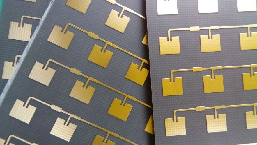
What to specify for RF-30A
Taconic RF-30A is covered here as a named RF material. RF-30, RF-30A and RF-30A2 are separate grade designations. Do not silently replace a historical RF-30 requirement.
| Field | Specification context |
|---|---|
| Material identity | RF-30A |
| Reference Dk | 2.97 |
| Reference Df | 0.002 |
| Test context | Dk: 1.9 GHz; Df 0.0020: 10 GHz (0.0013 at 1.9 GHz), modified stripline |
| Thermal conductivity | 0.42 W/m·K; see specimen/test condition |
| Supply status | Confirm current grade, thickness, foil and order quantity; no stock promise |
Do not miss: RF-30, RF-30A and RF-30A2 are separate grade designations. Do not silently replace a historical RF-30 requirement.
Reference trail: Supplier material reference · Grade data sheet · Processing guide. Numerical values are typical material references, not purchase acceptance limits, live stock or guaranteed fabricated performance.
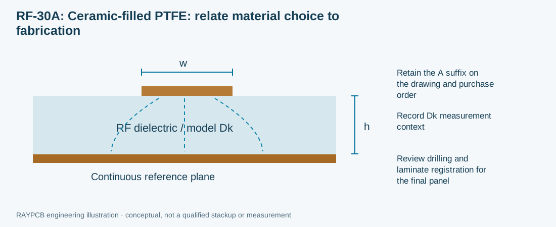
Ceramic-filled PTFE: relate material choice to fabrication
A ceramic-filled PTFE material combines an electrical and mechanical construction that must be identified by its full grade. A similar nominal Dk in another resin system is not sufficient for a drop-in change. The drilling, surface preparation, bonding and etching plan should be reviewed against the grade-specific processing guide.
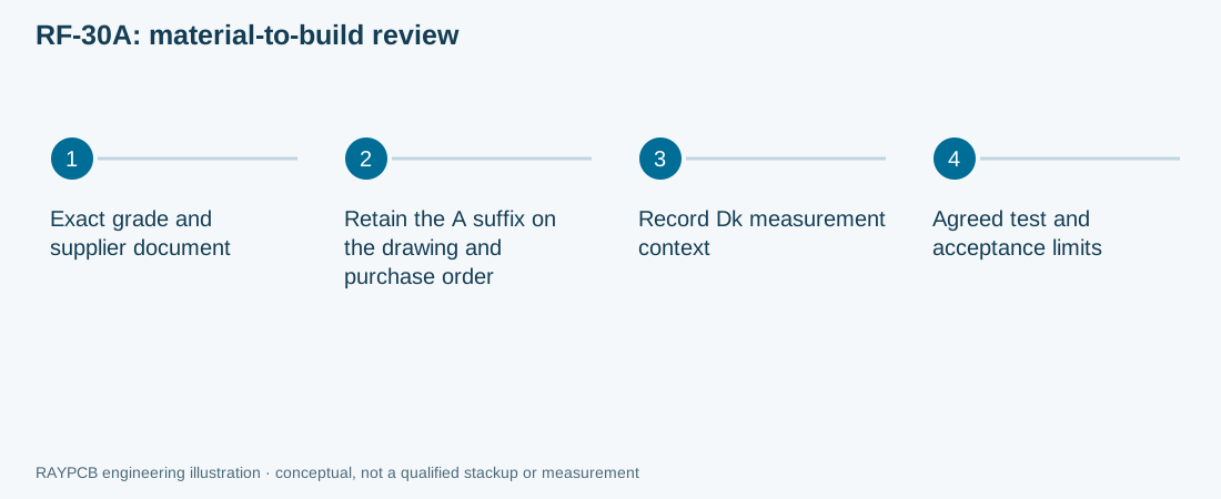
- Retain the A suffix on the drawing and purchase order
- Record Dk measurement context
- Review drilling and laminate registration for the final panel
RAYPCB ENGINEERING
Taconic RF EngineeringTaconic PCB Design Workbench
Loading Taconic PCB Design Workbench…
The RF tool uses an editable model Dk; the preset is a supplier reference at its stated method and frequency. It is not a universal design Dk. Blank parameters stay blank until you provide a value. Geometry calculations do not approve a fabrication tolerance.
For microstrip, h is the dielectric separation to the reference plane; for symmetric stripline it is the total plane spacing. Propagation follows λg = c/(f√εeff). Thermal screening uses R = h/(kA). Read the selected model’s exclusions beside the result.
For more geometries and fabrication tolerance context, use the PCB impedance calculator and design guide.
From material callout to fabricated PCB
01
Material release
Name RF-30A, the supplier revision, thickness and foil. Separate approved substitutions from suggestions awaiting approval.
02
CAM and stackup
Review layer references, panelization, copper balance, minimum features and finished geometry. Retain the A suffix on the drawing and purchase order.
03
Process definition
Use the applicable laminate and bonding guides. Agree drilling, hole-wall treatment and lamination details for this construction; do not assume a universal FR-4 recipe.
04
Patterning and final build
Control conductor geometry, hole quality, mask openings and finish on exposed RF areas. Include special edges, cavities or connectors in the release.
05
Inspection and acceptance
Define dimensional, netlist and impedance checks. RF loss or phase measurements need a separate coupon/fixture, frequency range and acceptance limit.
Review the manufacturing capability tables for general process limits and quality documentation and acceptance planning for supplier review. A listed material property is not a RAYPCB test report.
RF-30A PCB cost & quotation brief
A quote for RF-30A depends on the approved material construction, purchased sheet utilization, quantity, layer count, drilling/lamination work, finish and inspection scope. There is no defensible fixed “Taconic multiplier” across these products. For older designations, sourcing confirmation may be the first cost decision.
RAYPCB ENGINEERING
Taconic RF EngineeringTaconic PCB Cost & Quotation Brief
Loading Taconic PCB Cost & Quotation Brief…
Use the brief without prices, or enter your own setup and fabrication-area allowances to explore a simple two-layer planning range. The tool does not contain verified current supplier rates. Hybrid, multilayer, bonding-film and RF-qualified builds are routed to engineering quotation.
| Cost question | Information to provide |
|---|---|
| Material | Exact code, thickness, foil, substitutions allowed or prohibited |
| Fabrication | Gerber/ODB++, drill data, stackup, copper, outline and special features |
| Acceptance | Net classes, impedance target/tolerance and any RF test fixture |
| Order | Quantity, requested delivery date, repeat-build needs and assembly scope |
RF-30A questions before ordering
What does the RF-30A material name guarantee?
It identifies a material or family to resolve in the supplier documentation. The exact code, thickness, foil and data-sheet revision still need to be specified. It does not guarantee RAYPCB stock, lead time or an application qualification.
Which Dk should I use in my RF model?
Dk: 1.9 GHz; Df 0.0020: 10 GHz (0.0013 at 1.9 GHz), modified stripline. Use a model Dk appropriate to your geometry and frequency. A process test value is useful reference data but is not automatically the effective permittivity of a microstrip.
Can I replace RF-30A with another Taconic or Rogers grade?
RF-30, RF-30A and RF-30A2 are separate grade designations. Do not silently replace a historical RF-30 requirement. Compare the complete electrical, mechanical and processing requirements, then approve the alternate explicitly.
What design detail deserves the first review?
Retain the A suffix on the drawing and purchase order. Keep core and bonding-layer properties separate in the RF model.
Does a netlist test verify RF performance?
No. Netlist testing checks connectivity. RF performance requires defined measurement structures, frequency range, reference planes and limits. State the required measurement in the RFQ.
How do I obtain a usable quotation?
Send the fabrication files, drill data, stackup, exact material code, quantity and acceptance requirements. Include your requested date; the delivery commitment depends on sourcing and process review.
Next useful references: Taconic PCB manufacturing · full Taconic material directory.
Send the design with its material context
Preliminary files are welcome. Identify the design revision and open material decisions so the enquiry can address the actual manufacturing scope.
Send RF-30A files for review