Top 16 High Frequency Material Manufacturers for RF PCB Design

high frequency pcb

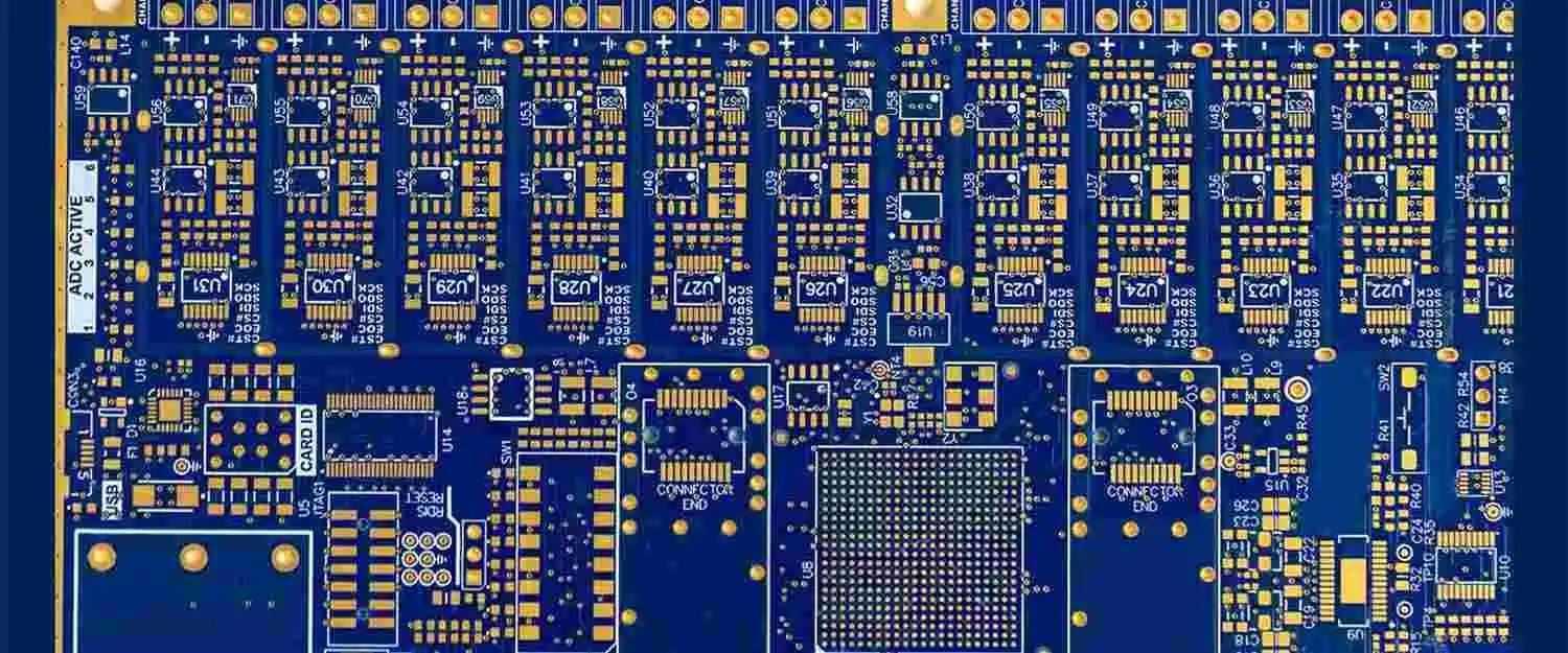
The selection of a material and its integration forms an important aspect of the fabrication of printed wiring boards. Our expertise concerning advanced material combinations and types helps us to deliver customers with the best solution for virtually all challenges related to PCB design.

Whether you desire a better dimensional stability or higher signal integrity, you can trust us to make the best recommendation that suits all packaging challenges.

There are several high frequency material manufacturers for RF PCB Design. We are going to consider 16 of them and the great qualities they possess.

16 High Frequency Material Manufacturers for RF PCB Design

Rogers

Rogers pcb circuit board

Rogers is highly regarded as a world technology leader having over 185 years of vast engineering knowledge. In addition, Rogers offers advanced elastomer components, DUREL drivers, and elastomeric material, connectivity, and different solutions for power electronics to markets all over the world.

Furthermore, Rogers is involved in the manufacturing of high frequency bondplys, laminates, and prepregs that are engineered to serve your performance requirements. The specialty materials of the company that feature a great dielectric constant control works best for aerospace applications, automotive radar sensors, 5G wireless communication, and satellites.

In addition, these materials are useful in these industries and applications. These include general industrial, connected devices, hybrid electric vehicles and electric vehicles, communication systems, and antennas. You can also find them in wired infrastructure, solar and wind, wireless infrastructure, and thermal solutions.

Rogers also has several bondply, prepreg, and laminate materials. These include 92ML materials, CuClad Series, CLTE Series Laminates, AD Series Laminates, IM Series Laminates, and DiClad Series Laminates. Others are Kappa 438 laminates, MAGTREX laminates, IsoClad Series Laminates, RT/duroid laminates, RO3000 Series, RO4000 Series, TMM laminates, TC Series laminates, and more.

Arlon

Arlon is a business owned by a veteran, which was established back in 1969. It is a main manufacturer of the specialty high performance prepreg and laminate materials that are used in different PCB applications.

Furthermore, Arlon specializes in some materials. These include epoxy products, low flow products, polyimide products, controlled thermal expansion, and surface mount technology. The company also offers low loss thermoset prepreg and laminate systems as well as controlled thermal expansion.

All these applications need laminates having specialized mechanical, thermal, or electrical, or other related performance features, which surpasses those of the standard FR4 materials. In addition, you can find these resin systems on different substrates. These include non woven aramid and woven glass.

In addition, there are some typical applications that these materials are suitable for. These include advanced military and commercial electronics like avionics, heat sink bonding, semiconductor testing, microvia PCBs, and high density interconnect.

The materials of the Arlon microwave deals in fluoropolymers, ceramic filled fluoropolymers, as well as ceramic hydrocarbon low loss thermoset laminates, which delivers the required electric performance in the circuit applications that are frequency-dependent.

DuPont

FULL PCB MANUFACTURING Quote

DuPont is a manufacturer or electronics materials having great comprehension of the advanced technology. It also has a huge industry expertise and knowledge, as well as a long innovation history. In addition, DuPont provides the largest high performance electronic materials in the industry and it is also proud to have one of the best manufacturing capabilities. Also, they have a great team that comprehends the best ways of creating solutions for customers.

Also, DuPont deals in the manufacturing of materials and substrates for the flexible and rigid circuits. These include polyimide films, materials for circuit imaging, and different laminates.

Concerning high temperature materials, DuPont is a great leader. This means they are great for high-temperature flex circuits that are useful in the automotive, oil, aerospace, military, as well as healthcare industries.

Using advanced fabrication techniques and equipment coupled with the high temperature materials of DuPont in fabricating the state of the art flex circuits, which has the ability to operate in different temperatures that are higher than 250 degrees centigrade. These solutions offer additional options regarding the solving of challenges of high temperatures.

Evonik

Evonik is known as one of the worldโ€™s largest companies that is devoted to special chemicals. ROHACELL, which is one product manufactured by them, is widely used in the fabrication of printed circuit boards. Furthermore, this ROHACELL is a structural foam, which has favorable transmission as well as very low dielectric constants.

This specific product is used in PCBs in these industries. These include aerospace, aviation, electronics, antennas, railcars, radomes, military, shipbuilding, automotive, leisure and sport, healthcare and medical technology, wind energy, and more. Furthermore, applications include mammography plates, CT machines, and X-ray and miniature antennas.

Evonik comes with other benefits, which includes a cell structure that is extremely fine, which ensures minimal uptake of resin as well as problem-free compatibility. The processing of fine-cell materials is possible by vacuum, prepreg, or layup infusion techniques, at a pressure of about 0.3 Mpa, as well as temperatures reaching 130 degrees centigrade.

Some companies make use of ROHACELL instead of the air spacer present in-between elements and radomes in the antenna application through the application of ROHACELL to the antenna PCB.

Hanwha

This company was established as a brand new corporation in year 2020. This company is highly regarded as a world leader when it comes to manufacturing chemicals and materials. In addition, the company has three main divisions, which include machinery, defense, and global.

Hanwa offers products and services for different industries, which include finance, solar energy, mechatronics, aerospace, construction, lifestyle/leisure, and finance. Some companies make use of the unreinforced polyimide, flexible laminate, which features copper clad on its two sides. Furthermore, it is useful as the main component of the construction of flex circuits.

In addition, Hanwha materials feature some processing benefits over the other manufacturers. Also, they could be very cost-effective.

Isola

This company is a global company that is fully focused on the design as well as manufacture of copper-clad laminates, as well as dielectric prepregs that are used in the fabrication of multilayer PCB. In addition, Isola is known to offer innovative solutions, as well as high quality solutions since the establishment of the company back in 1912.

Furthermore, with its history of great excellence, this company is known as the only provider of laminate with capabilities of research & development in Asia, Europe, and the United States.

The high performance materials of Isola are useful in some industries and markets. These include consumer electronics, storage, computing, and peripherals; medical, instrumentation, and industries; microwave and radio frequency; communications and networking; as well as transportation and automotive.

In addition, this company invests so much in its research & development. This is to develop important products that meet even strict performance requirements demanded from customers, original equipment manufacturers, designers, and PCB fabricators.

The Isola products include 370HR, FR406, FR408, FR408HR, P95/P25, P96/P26, G200, IS680-300, IS620i, IS415, IS410, GETEK, Green Speed, and 185HR. Others include 370HR, FR408HR, I-Speed, I-TERA MT40, I-TERA MT40 (RF/MW), Terra Green (RF/MW), Terra Green, Astra MT77, Tachyon 100G and a new product released in the second quarter of 2019 โ€“ IS550.

Megtron

Another popular material that is useful in the fabrication of printed circuit boards is Megtron. It is manufactured by the circuit board materials of Matrix, which was founded in 1977. Furthermore, Matrix is known to have four divisions, which are imaging products, carbide tools, chemicals, and laminates. Also, its technical team offering support possesses vast experience with all the parts of the manufacturing processes of the printed circuit board.

In addition, companies make use of Megtron 6 due to its low Dk (dielectric constant). It also has a better stability compared to the Teflon material. Furthermore, the Megtron 6 has low loss of transmission, low dissipation factors and a high heat resistance.

The design of these materials is for use in mainframes, high speed equipment, IC testers, as well as measuring instruments of high frequency. In addition, the Megtron 6 features great through hole reliability. Also, it works fine with lead free RoHS soldering.

Nelco

Nelco is a global entity, which is widely known for offering medical shielding, as well as industrial solutions and products. With respect to printed circuit boards, this company produces better mechanical and thermal performance materials. In addition, the company takes pride in its global leadership. Nelco is over 85 years old, and it has been offering unparalleled innovative solutions.

Nelco materials are all RoHS compliant. Many of these materials also offer CAF resistance and high thermal reliability for lead free assembly compatibility. In addition, this company offers lots of materials for fabrication of printed circuit boards. These include BT, Cyanate ester, Polyimide, as well as high speed and high Tg epoxy.

In addition, the PCB materials of Nelco are designed to serve printed circuit boards with a high layer count. It also includes high speed digital applications like lead-free assemblies, backplanes, automotive, wireless infrastructure and handsets, as well as networking and communications equipment.

Their hydrocarbon prepreg and laminates include HB-360, HF-350 FTC, HF-350F, HF-330F, and HF-300F. Also, they have lots of RF/Microwave materials as well as glass reinforced woven PTFE laminates, specialty materials, and prepregs/bond plies.

Ohmega

For over four decades, Ohmega Technologies has been able to manufacture OhmegaPly, which is a material that is useful in the construction of electronic devices. The company also has a well-known history of reliability and is fully focused on product enhancement and innovation.

Some companies make use of OhmegaPly as the resistors layer that are created making use of the standard PCB print as well as etch process. The technology permits the designer to be able to free space on the PCBโ€™s surface through the embedding or buying of the resistor components.

In addition, the material serves as a โ€œblank slateโ€™ offering a PCB designer with the main tool for looking into electronic issues that require passive resistive films or resistors. Also, OhmegaPly is useful in some PCB applications. These include military and aerospace, which includes missiles, space probes, satellites, aerial vehicles, and fighter aircraft. Also, they are applicable in consumer products like microphones and cell phones.

Panasonic

Panasonic MEGTRON M R-5735 PCB

This company is a well-known technology company all over the world. They are also recognized as oje of the leaders in the world of electronics. They offer different services and products. These include smart mobility, industrial devices, tablets, computers, AV solutions, and more.

This company manufactures PCB materials, advanced films, and more. Due to the advance of PCB technologies and semiconductor, this company has met the needs of customers by creating optimum materials that will serve next generation technologies. Among them are technology for the design of compound material, technology for materials evaluation, as well as resin design technology that serves state of the art electronics.

As a result of their high-quality assurance system that integrates the methods of manufacturing management like SPC, this company can supply the multilayer laminates or materials, which satisfies the needs of customers by making use of different evaluation technologies.

The materials of Panasonic can be seen in many PCB applications. These include appliances, mobile products, and network antenna.

Sheldahl

This high frequency material manufacturer is seen as a leader in the industry in the deposition of thin film on adhesive formulations, flexible materials, patterning, finishing, and laminations. All these are produced in completely high volumes and done using the latest technology and equipment.

With over 65 years experience, this manufacturer boasts of being a leader in the industry, which delivers consistently on great quality as well as great customer satisfaction. In addition, the brand materials of Sheldahl are made up of different specialty products. These include flexible laminates, cable tapes, high performance splicing tapes, advanced coated films, and flexible materials for different global markets.

In addition, they can process substrates that are as thin and thick as 1.5 micrometer and 350 micrometers respectively. Sheldahl manufactures circuits and materials for different industries. These include medical, health solutions, defense and aerospace, automotive, heaters, human machine interface, consumer, and industrial.

Taconic

This manufacturer is a global leader when it comes to the manufacturing and development of advanced composite materials. They manufacture high quality pcb materials for various industries. Taconic is known as a leader in PCB materials supply due to their high commitment to great customer service. This also includes their zeal to deliver reliable and high quality materials. Also, it includes the ability of the company to work in line with the changing needs of the industry.

Having started the production of PTFE coated fabrics, as well as other non-stick and high temperature materials, this manufacturer is now one of the best suppliers for the industry of food processing. Also, they supply many different coated materials, which include belts, fabrics, and tapes for different industrial applications.

Also, Taconic offers advanced materials for high-speed, RF, and microwave digital applications. These include Telecommunications (transmitters, power amplifiers, splitters/filters/combiner/components, base station antenna/antenna) and automotive (monitoring tire pressure, high temperature reliability, cruise control).

Others include military (telemetry, radar, and guidance systems), multilayer (satellite, RF multilayer, digital multilayer, and Chip/ATE testing. We also have mechanical (gasket, Flex PCB assembly, and non silicon masking tape), and medical (medical scanners, and wireless body area network).

Ventec

Ventec is known as a global leader when it comes to producing high performance and high quality copper clad prepregs and laminates. Through its U.S. and European subsidiaries, this company provides local services to its customers through its global reach. It also delivers complete research & development and development capabilities.

Ventec offers different products, which serve the copper clad laminate and prepreg markets. These include a complete range of different polyimide products that includes prepregs that suit hole filling (with no-flow and low-flow options).

Commonly, Ventecโ€™s FR-4 material is very useful for daily PCB fabrication. It is possible to manufacture the high quality epoxy glass prepreg and laminate material in custom as well as standard core thicknesses. Typically, they are useful in high and low power applications and they are well known for their great dielectric properties and high Tg.

Furthermore, these Ventec materials for PCB are very useful in different applications. The common Ventec materials include -5A2, Tec-speed 20.0, VT-901, VT-4B series, VT-47, and standard FR4.

Tatsuta

This company is fully focused on conducting research as well as meeting the needs of customers via sustainable processes. Established as the electric cable and wire business, this company supplies electric cables and wires of high performance coupled with functional materials that are used in bonding wires, printed circuit boards, medical products, sensors, etc.

The value materials of the company play a major role in advanced technology. Furthermore, Tatsuta produces many optical components and electronic materials, like FFC application films, EMI shielding film, optical fiber couplers, and conductive paste.

Some companies make use of the CBF300 and AE3030 materials of TATSUTA. Both materials are copper pastes that are useful as a non-conductive or conductive material for via hole fill. In addition, these materials feature a thermal conductivity that is very high. Also, they are highly efficient in constructing thermal vias in many high heat applications.

ThinFlex

ThinFlex is another company involved in the manufacturing of high frequency materials. This company is based in Taiwan and is involved in manufacturing and distributing coverlays and FCCLs (flexible copper clad laminates). ThinFlex has gained a wide reputation due to its excellence.

Furthermore, one product from the company that takes the same name, made a great mark on the PCB market. Due to its recognition for its cutting-edge and innovation technology, this company is ranked among the best in the IC and FCCL packaging industries.

ThinFlex manufactures single-sided adhesiveless copper clad laminates as well as double-sided adhesiveless copper clad laminate. This single-sided type is well known for its excellent textural endurance, great dimensional stability, and high tensile strength. On the other hand, the double sided type is well known for its great chemical and heat resistance, etching capabilities, as well as high flexural endurance.

Flexible copper clad laminates are applied during the manufacturing processes of some applications. These include medical equipment, cell phones, cameras, LCD panels, aerospace products, fax machines, printers, computers, photocopiers, scanners, and industrial equipment.

You can apply coverlays during the manufacturing of notebook computers, cameras, printers, household computers, cell phones, scanners, and more.

Ticer

Ticer technologies was established in 1884. However, back then it was called Gould Electronic Materials. Now, this company has become one of the best manufacturers of the electrodeposited copper foil.

Later in the year 1999, Gould created TCRยฎ, known as the resistor technology. Furthermore, this material which is included among those of the next-generation helps in providing solutions for aggressive, new applications. Furthermore, it meets the demands relating to performance of the advanced PCBs (printed circuit boards). Letโ€™s go on to consider what the Ticer material is, as well as their applications.

Ticer technologies is known to produce high performance, thin film embedded-resistor copper foils for RF and digital PCBs (printed circuit boards).This next generation technology for embedded resistors is best suited to help in meeting challenges that are posed by new materials and designs  and increase the performance requirements both for future and current electronic packages.

Enhanced as a result of the reliability and capability of TCR, the solutions of Ticer make use of the most recent with respect to laminate systems that are advanced.

Asides from its being RoHS-compliant, the TCR works fine with different resin systems, which includes high performance, standard, specialty, and lead-free products. In addition, TCR also increases the space that is available for the components. It also helps in reducing the PCBโ€™s weight, and overall, it improves the performance of the product. Also, regarding the thermal stability, it provides an exceptional one.

Conclusion

The above are the 16 companies involved in the manufacturing of high frequency materials. All the materials these manufacturers produce are of top-quality and they are useful in different applications. If you need assistance and guidance regarding your choice of material, you can contact us. We at RayMing PCB & Assembly will answer all questions and attend to all your needs. Also, we work with the best materials that suit the PCB needs of customers.

Ohmega Materials in PCB Manufacturing

Ohmega Materials

Ohmega technologies have been producing materials for PCB manufacturing over the years. This company focuses on product enhancement and innovation. The increasing demand for high speed PCB packaging has led to the use of embedded passives in PCB designs.

Ohmega materials have become the best choice in circuit applications. These materials are globally used as a cost effective and high volume alternative to other PCB materials. Also, there are several benefits of integrating Ohmega PCB materials in PCB fabrication.

Types of Ohmega Materials

FULL PCB MANUFACTURING Quote

OhmegaPly

The OhmegaPly is a thin film planar resistor used in PCB manufacturing. It is an embedded layer of resistors created with an etch process and a standard PCB print. This resistor enables designers to maximize space on a PCB surface. This Ohmega material functions as a blank state that offers designers means to address contemporary electronic challenges that require passive resistors.

OhmegaPly comprises a film resistive alloy layer and a copper-conducting layer deposited on a copper foil. Also, this material comes in different standard sheet resistivities. PCB manufacturers can bond this material to any dielectric material.

Furthermore, a wide range of applications has been integrating OhmegaPly since the 1970โ€™s. For the past decades, this material has featured long-term reliability and stability. Also, it has become a good alternative to other embedded resistors. The OhmegaPly resistors in designs are widely used in advanced applications.

Also, ohmegaPly comprises nickel-phosphorous (NiP) alloy. During the production process of this material, the engineer electro-deposits about 1.00 microns of alloy on the copper foil. This copper foil is electrodeposited. This Ohmega material is available in 50 ohm per square , 10 ohm per square, and 100 ohm per square at +-5% tolerance, +-3% tolerance, and +-5% tolerance respectively.

OhmegaPly offers both cost and design advantages. The elimination of discrete resistors help engineers to realize cost saving benefits. Also, higher resistor density indicates more cost savings. This Ohmega material is widely used in several applications. Some industry leading OEMs like Apple, Advance Fibre, and Boeing integrate these resistors in their products.

Also, the resistorโ€™s size and the type of dielectric material determine the amount of power applied. The typical power rating of OhmegaPly is about 1/8 watt. However, the use of laminate materials with higher temperature can increase this rating.

Ohmega ฮฉ Resistivity Meter

This is one of Ohmega materials used in PCB fabrication and electronics manufacturing. Ohmega ฮฉ is a portable earth resistivity meter that can measure resistance over a wide range of conditions. Also, this material has proved its performance in temperatures beyond 45oC. Also, Ohmega ฮฉ is specially designed to enable easy use.

An impact-resistant Peli case houses the Ohmega ฮฉ resistivity meter. This Peli case features a lifetime guarantee, therefore, it replaces catches and broken handles for free. When this material functions in unfavorable wet weather over a period of time, it can corrode. Also, Ohmega ฮฉ comes with a battery charger and 4 stainless steel electrodes.

Benefits of Ohmega Materials

Ohmega materials offer a wide range of benefits when used in circuit boards and electronics. For years, Ohmega has been delivering high-quality materials to PCB manufacturers and OEMs.

Improved signal integrity

Ohmega materials offer a high signal integrity in applications. With good quality electrical signals, these materials operate at high frequency and high speed. Also, high signal integrity is crucial for enabling data to pass between PCB components. Also, these materials allow interpretation of signals by a receiver component.

Greater reliability

Ohmega materials feature high reliability and stability. Also, the electrical and thermal properties of these materials are responsible for their performance and reliability in applications.

Reduced surface EMI

EMI shielding is crucial in any electronic circuit. Ohmega offers electromagnetic interference shielding materials. Electromagnetic waves usually occur when there is a contact between an electric field and a magnetic field. EMI occurs when external radiation or conduction generates a disturbance which affects an electrical circuit. However, Ohmega materials protect circuits from electromagnetic interference.

Low insertion loss

The OhmegaPly features exceptional low insertion los and excellent stability due to the nature of the copper foil integrated. This material has proved that it can operate beyond 40 GHZ

Improved inductive reactance

Ohmega products offer a high level of inductive reactance. For instance, the Ohmega ฮฉ offers improved inductive reactance. Inductive reactance measures the opposition to a current change. Therefore, it is an electrical property that opposes current.

Applications of Ohmega Materials

The OhmegaPly is widely used in various RF and microwave circuits. Asides from that, it is suitable for use in advanced applications.

Telecommunications

You will find Ohmega materials in telecommunication switching cards, antennas, and cellular telephone modules. These materials offer absolute reliability and as such, are ideal for use in the manufacturing of telecommunication devices.

Consumer electronics

The OhmegaPly is a great material for consumer electronics. This material is available in computers, smartphones, and microphones among others. Also, OhmegaPly can replace discrete resistors and as such, offers great performance in this application

Military and aerospace

The military and aerospace industries rely on Ohmega materials. Also, these industries integrate these materials in their devices. Military supercomputers and unmanned aerial vehicles comprise Ohmega materials. Also, in the aerospace sector, Ohmega materials offer a wide range of benefits. You will find them in fighter aircraft, space probes, and more. These materials offer great electrical and thermal properties, ensuring great performance in aerospace devices.

Medical electronics

Ohmega materials have impacted the production of some medical devices. These materials are ideal for use in this application due to their properties and benefits. Also, these materials offer high frequency and reliability. Medical devices like pacemakers, cardioverter defibrillators, and more feature Ohmega materials. OhmegaPly reduces EMI and noise produced by other components. Therefore, it offers great performance in medical devices.

Conclusion

There are several benefits of integrating Ohmega materials in PCB fabrication and electronics manufacturing. These materials have become very popular in the PCB and electronics industry. Also, they offer great thermal and electrical properties. Ohmega has been delivering high-quality products over the years.

How the Megtron 6 PCB Laminate Material Benefits Your PCB Projects

Megtron 6 pcb

So many types of materials and laminates are useful for both computing and industrial applications. These include building PCBs (printed circuit boards). This process of bonding lamination has to do with the building of many layers into waterproof so as to protect and strengthen different substances.

These internal layers are also placed on extreme temperature and pressure to help in slowly curing, releasing, and cooling the material in order to create the multilayer PCBs. Particularly, Megtron 6 PCB is a durable and highly efficient laminate, which is seen in so many printed circuit boards (PCBs). If you have been wondering if you should make use of the Megtron 6 PCB material, then keep reading to know their benefits, as well as ways where they can make your products better.

What Is Megtron 6 PCB Laminate Material?

Megtron 6 PCB Material is a high-speed laminate material that is useful in different PCB fabrication types. You will also find them useful in PCB fabrication, as well as manufacturing for so many applications. This basic material has been designed to serve many high frequency instruments for measurement, mainframes, and integrated circuit testers.

Also, the Megtron 6 PCB Material features a thick layer count, low transmission loss, as well as so many layers that helps in enhancing a high speed network equipment. Furthermore, the laminates feature electrical properties, which rival the PTFE material. This is possible thanks to their unique benefits and high processability.

Furthermore, making use of the Megtron 6 PCB laminates makes sure the performance of the system is enhanced in so many fields. These include router, high speed transfer, telecommunications, and computing applications. In addition, the Megtron 6 PCB material sheets feature increased stability, high-density interconnect, high thermal resistance, and low dielectric constant.

Furthermore, they also work fine with lead-free soldering. They can avoid signal reflections at very high frequencies having low-profile foils for the RF PCBs. In order to produce the Megtron 6 PCB laminate, the two conducting materials majorly copper, as well as insulating materials like the fiberglass epoxy materials are usually used.

We have explained some of the features of the Megtron 6 PCB Material. Now, let us consider the major attributes, which helps in distinguishing this particular material from the other Megtron Laminates

Main Features of the Megtron 6 PCB Material

FULL PCB MANUFACTURING Quote

Below are the main features of the Megtron 6 PCB Material

Low dielectric constants

A low dielectric constant is great for high-frequency and power applications. This is because they help in reducing loss of electric power. Furthermore, these laminates feature great properties, which help in increasing electrical conductivity. With their dielectric constant of about 3.7, they feature less current storage, thereby making them great for these applications.

Low dissipation factor

Low dissipation factors reveal how much a specific material can hold energy or behave like an insulating material. The lower this dissipation factor value, like the Megtron 6 PCB laminates, the more efficient its insulator system will behave. The Megtron 6 PCB Material has a low dissipation factor, which stands at 0.002. This provides reduced leakage of the electric current during operations.

High Heat Resistance

The Megtron 6 PCB laminates have the ability to withstand a large amount of heat. This is due to their great dissipation features. You can be very sure that making use of these sheets for different applications in harsh and extreme temperatures, or with some thermal clads, without damaging the surfaces or creating any dangerous environment.

Low loss of transmission

Many printed circuit boards need materials with a low loss of transmission. This helps in reducing the conductor and dielectric loss necessary to achieve the PCB materials demand. Fortunately, the Megtron 6 PCB laminates have a low loss of transmission. This makes them great for these applications.

What are the Applications for the Megtron 6 PCB Laminates?

The Megtron 6 PCB Material is best suited for the following applications.

High speed network equipment

The Megtron 6 PCB laminates are useful for any communication equipment. This is because it helps in improving operations on different devices for interconnect routing and local area networks.

High frequency measuring equipment

The Megtron 6 PCB laminates are great when operating this equipment. Every time, they will offer very accurate results.

High speed IC testers

The Megtron 6 PCB laminateโ€™s mechanical properties help the IC testers in offering very efficient and accurate results during the testing of other integrated circuits.

High speed mainframes

Computer systems or high speed mainframes which help in processing large data can get some benefit from the Megtron 6 PCB laminates. This is because they help in increasing the devicesโ€™ efficiency. This is possible through the maintenance of the system and then ensuring it runs at an optimal operating condition.

What are the Benefits of Megtron 6 PCB Laminates?

The Megtron 6 PCB laminates work efficiently in offering lots of benefits for many different applications. Below are the main benefits of making use of the Megtron 6 PCB laminates.

High Efficiency Rates

Working with the Megtron 6 PCB laminates, you will be able to see accurate results and work more efficiently. This will happen without you having to compromise on the performance standards for the high-frequency applications.

Through Hole Reliability

These laminates feature excellent resiliency and through hole reliability. This makes them great for several applications. Furthermore, through hole components allow these components to be able to endure a high environmental stress thereby creating a stronger connection between the layers.

High Electric and Thermal Conductivity

The Megtron 6 PCB laminates are great insulators. They can enhance proper electrical currents flow, coupled with reducing the leakage present in electric and thermal applications. In addition, these laminates also facilitate enhanced heat conductivity thereby improving efficiency and productivity.

Very Durable

This laminate is very durable. Their strength permits the material to be able to hold as well as stay useful for very long periods.

Conclusion

The Megtron 6 PCB Laminate has great features and that is why it is useful in different applications. It will definitely be useful for your PCB projects.

General Properties and Applications of the Megtron 4 PCB Laminate

Panasonic HEPER R-1755E PCB

The task of choosing an appropriate Megtron 4 PCB laminate could be overwhelming. This is why we will be making everything easy for you. We will explore the basic aspects of these laminates.

In this article, weโ€™ll explain what they are, their general properties, benefits, applications, and more. Please stay on this page to understand the topic better.

What are Panasonic Megtron 4 PCB Laminates?

The Megtron 4 PCB laminates is a multiple layer PCB material having low loss of transmission and is very heat resistant. Furthermore, the Megtron 4 PCB laminates are useful in protecting your PCB from effects of water, dust, and excess heat.

General Properties of the Megtron 4 PCB Laminates

The Megtron 4 PCB laminates have both extensive and intensive factors, which reveal the way they function in their different environments.

Also, you must make sure that the Megtron 4 PCB laminates have such properties in them to ensure the laminates have proper authenticity

Below are the general properties of Megtron 4 PCB laminates, which you must consider

Chemical Properties

For the chemical properties, youโ€™ll be considering the Megtron 4 PCB laminates properties whenever they are exposed to some chemical elements

Some important chemical properties you need to consider are reactivity, flammability, toxicity, combustion, acidity, and more

Thermal Properties

For the thermal properties, you have to consider how the Megtron 4 PCB laminates reacts hen exposed to very high temperatures

What we mean is that, youโ€™ll consider all the Megtron 4 PCB laminates properties with respect to heat conductivity. The features you must consider are thermal conductivity (denoted as k), coefficient of thermal expansion (denoted as CTE), and decomposition temperature (denoted as Td).

Mechanical Properties

The mechanical properties refer to Megtron 4 PCB laminates physical properties, which you can observe after applying a force on them. Some mechanical properties you have to consider are tensile strength, elongation, fatigue limits, elasticity, and modulus.

Benefits of Making Use of Megtron 4 PCB Laminates

FULL PCB MANUFACTURING Quote

Consider making use of the Megtron 4 PCB laminates as a result of the many benefits of making use of the laminates. Below are some of the benefits you will get when making use of the Megtron 4 PCB laminates.

Low dielectric constant

The dielectric constant of the Megtron 4 PCB laminates is very low. It has insulating materials, which stores charge between the different metallic plates. With this, the Megtron 4 PCB laminatesโ€™ electrical conductivity will increase. This improves the general performance of these PCBs (printed circuit boards).

Lead Free Soldering

This Panasonic laminate is one of the safest with the lead free soldering. This is what makes it environmentally friendly. Furthermore, you can use it without getting scared that it may hurt you or case pollution to the environment.

Dielectric Dissipation Factors

For this, youโ€™ll enjoy the Megtron 4 PCB laminatesโ€™ dielectric dissipation factors which boosts their performance generally. Furthermore, at 1GHz, the Megtron 4 PCB laminates has a dissipation factor and dielectric constant of 0.005 and 3.8 respectively

High Heat Resistance

For applications that are heat laden, you will work with your machine as these laminates assist in resisting much heat. In addition, it works with thermal clads that conducts heat from your appliance therefore making them very cool.

Quality Compliant

As a result of the high quality features and properties of the Megtron 4 PCB laminates, you can use them for long periods. As a result of quality compliance, you can use it because it doesnโ€™t produce any toxic material.

Through-Hole Reliability

The Megtron 4 PCB laminates feature great through hole reliability, which is much better compared to the FR4 materials. Drilling the through-hole in the Megtron 4 PCB laminates in a manner that is more reliable is easier compared to others.

Low loss of transmission

During the electric currents transmission from a point to another point, you will be able to experience extremely low losses of transmission. Furthermore, there is very little leakage of an electric current via the Megtron 4 PCB laminates.

What are the Applications of the Megtron 4 PCB Laminates?

Youโ€™ll make use of the Megtron 4 PCB laminates when manufacturing different PCBs (printed circuit boards). This provides the PCBs with the appropriate features in performing appropriately in some applications.

Below are some applications whereby the Megtron 4 PCB laminates are useful.

Communication Industry

The Megtron 4 PCB laminates are useful during the lamination of PCBs to be used for communication purposes. It offers PCBs with appropriate conduction and insulation properties to ensure the right data transfer.

Medical Industry

For this industry, youโ€™ll utilize the Megtron 4 PCB laminates in manufacturing printed circuit boards that are useful for different medical appliances. Its thermal properties can work appropriately in some high-thermal medical applications like radiology machines.

Automobile Industry

For the world of automobiles, you can use the Megtron 4 PCB laminates in some appliances. Furthermore, it enables proper lighting, communications, and data transfer in different automobiles.

Materials Used in Manufacturing the Megtron 4 PCB Laminates

Here, there are some materials that are useful in manufacturing the Megtron 4 PCB laminates. One of such materials that you will find on these laminates is the fiberglass epoxy material. You will make use of this fiberglass epoxy for the construction of Megtron 4 PCB laminates due to its great insulation properties.

Furthermore, the fiberglass epoxy features polystyrene core materials, which prevents electric current leakage. Also, you can make use of it with conductor materials like aluminum and copper that helps in offering these dielectric properties.

Asides from this, fiberglass epoxy features the most appropriate flex out in the waves, and will be able to survive the different conditions of the environment. Also, you can make use of epoxy resin to serve as the major insulating material during the manufacturing of the Megtron 4 PCB laminates.

Processing Technology Used for Manufacturing the Megtron 4 PCB Laminates

When making or manufacturing the Megtron 4 PCB laminates, youโ€™ll utilize some manufacturing technologies. Out of all the technological processes, the most common of them is called the electrolytic foil process of manufacturing.

This manufacturing technology is very important because it helps to include the materials of the copper foil into the fiberglass epoxy. This is also called the electrolysis principle.

Conclusion

Megtron 4 PCB Laminates is a high-quality material with lots of benefits and different applications. You can try them out today and discover if it works for you.

Evonik ROHACELL Materials for PCB

Evonik ROHACELL PCB

For more than 40byears now, Evonik has been providing a wide range of products for several industries. The PCB industry has benefited from the products manufactured by Evonik. Also, Evonik ROHACELL offers solutions for various applications for fiber-reinforced composites. Most of its composite products are mainly used by aviation, construction, wind power, and automotive industries.

Evonik has been offering several industries unrestricted possibilities for lightweight manufacturing of products or parts made from composites. ROHACELL is one of Evonikโ€™s products commonly used in the fabrication of printed circuit boards. We will be focusing more on Evonik ROHACELL and its usefulness across industries.

What is Evonik ROHACELL?

ROHACELL is one of Evonikโ€™s several products. It is lightweight structural foam used in the manufacturing of PCBs. Also, this foam has very low dielectric constant and offers favorable transmission. Evonik ROHACELL is widely used across a wide range of industries. This product features very fine cell structure which enables compatibility with metallic materials. Also, it has minimal resin uptake and no corrosive effects.

Furthermore, Evonik ROHACELL is a fiber-composite that offers an extraordinary low-loss barrier. This barrier is much better than that of air. Also, this foam is ideal for use in advanced RF/Microwave PCBs. ROHACELL foam offers high temperature resistance of about 220oCand exceptional dynamic strength. This lightweight foam is easily machined.

Also, this foam is usually attached to circuit boards. Engineers have devised several ways of attaching this composite in PCBs. In addition, Evonik ROHACELL offers high pressure resistance even at increased temperatures. Also, these foams are very effective, especially at very high processing pressures and temperatures. They are cost-effective materials for PCB fabrication.

You can cure Evonik ROHACELL at high temperatures since it features high creep and thermal resistance. RoHACELL is polymethacrylimide-based foam that offers creep compression strength and great mechanical strength superior to other rigid foams. This material is often integrated as a structural core. Also, its stiffness is useful for winding, performing processing, and braiding.

Engineers can integrate ROHACELL to build a complex sandwich design. This helps to ensure a stable and efficient process. Also, this material is well-known for its unique properties and benefits.

Features of Evonik ROHACELL

FULL PCB MANUFACTURING Quote

Evonik ROHACELL offers a wide range of unique features which include:

Low weight

ROHACELL is a lightweight structural foam. Its lightweight feature makes it a suitable core sandwiched between plastic skins of fiber composite. Also, its low weight saves more energy and as such, enables environmental protection.

Exceptional dynamic strength

This structural foam has great dynamic strength. Also, you can apply pressure on this material repeatedly. Therefore, it is ideal for use in applications exposed to high pressure and temperature.

Exceptional mechanical properties

Due to its great mechanical properties, it is suitable for composite structures. Also, ROHACELL offers exceptional mechanical properties at low densities and over a wide range of temperatures. This structural foam offers high mechanical performance at an extreme low weight.

High creep resistance

ROHACELL offers extraordinary compressive creep properties for processing of about 190oC. Due to its high creep resistance, you can cure this material at very high temperatures. ROHACELL is the only core material that provides such fast curing.

High temperature resistance

ROHACELL offers an excellent temperature resistance of about 210OC in post-cure processes. Also, this foam is a unique core material that has proved to withstand high pressures and processing temperatures.

Benefits of Using Evonik ROHACELL

Cost-effective

Evonik ROHACELL is a cost-effective alternative for composite foams. It can be easily processed. Also, it provides cost savings in the production of a complete component.

Versatile

One of the main benefits of ROHACELL is its high-end versatility. Also, this lightweight structural foam is ideal for use in a vast range of applications and industries. From aviation to communication and medical, ROHACELL has proved to be a reliable core material.

Easily machined

This structural machine can be easily machined. There is design freedom for engineers who integrate ROHACELL. You can shape the foam using thermoshaping, machining, or thermoforming.

Customizable cell sizes

The cell sizes of ROHACELL are customizable to various processing methods. You can choose from different cell sizes. Also, ROHACELL comprises closed cells. This material features no heavy metals or CFC.

Applications of Evonik ROHACELL

Evonik ROHACELL is widely used across several applications and industries.

Medical technology

ROHACELL plays a crucial role in the manufacturing of medical technology equipment. This structural is a core material in CT scans and patient tables for X-Ray that minimizes patientsโ€™ exposure to radiation in diagnostic procedures. Therefore, it helps to prevent unfavorable effects on human health while offering great image quality for accurate diagnosis.

Wind power

ROHACELL is widely used in wind turbines. For example, expanding offshore and traditional offshore both have foam core in their blades. This foam core is lightweight which helps to reduce load. Also, lighter blade in turbines help to extend their service life.

Electronics and communication systems

Radar devices carry out several positioning and navigation tasks during flight operations. Antenna devices such as cover of radar are specially designed as a composite structure. This cover must possess some mechanical requirements due to exposure to external factors and high speeds. ROHACELL offers dielectric properties that meet requirements of the radar system. Also, ROHACELL is widely used in mobile phonesโ€™ loudspeaker membranes.

Transportation

ROHACELL is ideal for use in several modes of transportation like trains and ships. Its lightweight nature offers several advantages in the air and on the road. Cars, ships, trains built with lower weight materials save fuel and also enable minimized emissions. Reducing the weight of vehicles is a great advantage for electric cars as it helps to improve range. Also, you will find Evonik ROACHELL in advanced racing cars.

Aviation

ROHACELL has played a significant role in the aviation industry for a very long time. It is a light and efficient alternative to metal materials. For instance, rotor blades of helicopters feature ROHACELL. The sandwich design protects the rotor blades from local buckling.

Conclusion

Evonik ROHACELL is a high-end core material in PCBs and other electronics. It serves a wide range of functions and offers unique benefits.

Characteristics and benefits of HUBER+SUHNER RF Components

RF Components

RF passive components are helpful in the transmission of electromagnetic energy. As a result, these components are useful in various applications and platforms. For example, they are necessary for aircraft for flight tests and telemetry applications, missile experiments, data link communications, robots, and electronic warfare systems. They are also ideal for wireless communications between aircraft.

We can use RF passive components in wireless communication base stations and indoor distribution systems. These systems provide continuous coverage of wireless signals indoors by splitting the signal from a base station. To achieve this, we distribute the signal to the antennas of coverage points. The antennas of the coverage points then receive the signal, achieving continuous indoor coverage.

Passive components can control the flow of energy in a circuit. In contrast, active components are devices that produce electrical signals. These devices include transistors, silicon-controlled rectifiers, and diodes. Active components require an external power source to function. On the other hand, passive components influence the flow of power without requiring an external power source.

The RF Unit

An RF unit is a device that emits radio frequency waves. These devices are commonly in power lines and streetlights. There are several ways to protect yourself from this radiation. One way is to de-energize the RF unit and then work around it. Another way is to maintain a safe distance.

Another form of RF unit is a mobile device. These devices can move from location to location. They are often suitable for use with at least 20 cm separation from the transmitter and the user’s body. Some examples of mobile devices include smartphones and tablet computers. These devices can connect with other devices.

RF components are also helpful in televisions and media players. These devices use RF modulators to change the signals they receive. These devices can change audio and video signals from any source. This way, you can control how much output you get. Sometimes, you can control how much power your television can handle.

The FCC regulates RF components. They are classified based on their components and devices and are subject to different rules. Therefore, you can incorporate an RF module that meets the applicable requirements to avoid violating FCC rules.

The RF Circuit in low noise amplifier

An RF circuit is an electronic device that uses radio waves to transmit information. It is highly sensitive to noise, such as voltage glitches. To reduce the chance of failure, one should design it so that it can withstand voltage glitches and still perform its function. For this reason, it is essential to place decoupling capacitors strategically. For example, if a circuit contains an IC component, it should have two decoupling capacitors placed in parallel with the component.

RF PCBs are becoming increasingly popular in mobile phones and cellular networks. As a result, they have evolved from simple thick copper-clad boards to multilayer PCB that can handle higher frequencies. These multilayered boards are made of thin copper layers and are incredibly flexible. This makes them easy to integrate into mobile devices and other space-constrained equipment.

An RF circuit is a complex device that uses active devices to adjust signal frequencies. It includes various components, low and high-power amplifiers, modulators, and demodulators. An amplifier increases the voltage of an RF signal, typically to a few millionths of a volt, while a modulator alters the RF carrier’s frequency. A demodulator, on the other hand, extracts information from the modulated carrier.

RF Circuit Design

RF design involves the placement of decoupling capacitors. The simplest circuit has two decoupling capacitors placed in parallel with an IC component. Each capacitor should be on the same layer as the other. The decoupling capacitors should also have individual ground vias. In addition, they should be in ascending order of their capacitance from the power supply. This means that the lower capacitance capacitor should be closest to the power supply.

RF componenets operate at high frequencies and high power levels. With higher frequencies, these constraints become even more critical. In addition, the reactance of the signal traces becomes increasingly essential. As a result, microwave circuits require much more power than a conventional circuit can handle. The physical layout of the circuit must account for this.

RF circuits are ideal in many applications, but wireless communication is one of the most popular. The block diagram in figure a shows a typical wireless communication system. Figure A shows the receiver and transmitter circuits. It also shows the digital processing part that processes the digital signal.

Types of Active radio frequency Components in Circuits

There are two basic types of active components: voltage-controlled devices (VDS) and current-controlled devices (BJTs). Voltage-controlled devices operate by supplying energy to a circuit whenever the current leaves the positive terminal. Current-controlled devices are constant, nonvolatile sources of current which control the flow of charge in the circuit.

On the other hand, passive components cannot control the flow of electricity, although they can store energy, produce an inductance, and resist the electric current. Both types of active components are commonly used in every electronic device and have a variety of applications. Some active components include computing power, built-in batteries, and LED lights.

Active components, which include diodes and integrated circuits, can be used in RF circuits. They are also helpful in other circuits, such as analog and low-frequency digital circuits. However, RF circuits are different because their designs require different objectives and challenges. They may also use integrated circuits that perform functionality unique to RF systems. In addition, they may be unfamiliar to designers unless they’ve worked with RF circuits for a long time.

The two main types of RF circuits include power amplifiers and low-noise amplifiers. A power amplifier provides power and a low noise figure, while a low-noise amplifier provides a high voltage gain and low noise figure. In addition, both RF circuits typically include a mixer that mixes two signals: the transmitter mixer and the receiver mixer. Finally, a filter controls the signal energy and is essential for preventing cross-talk between radio signals.

HUBER+SUHNER Components

FULL PCB MANUFACTURING Quote

HUBER+SUHNER is a company that develops and manufactures radio frequency and microwave components. Their products include Broadband directional couplers, Fixed attenuators, and RF-over-Fiber modules. They are also certified by ISO 14001, TS 16949, IRIS, and EN(AS) 9100.

HUBER+SUHNER develops and manufactures radio frequency and microwave components

HUBER+SUHNER is a Swiss-based company that develops and manufactures components for optical and electrical connectivity. The company’s products serve the Communications, Transportation, and Industrial markets.

The company’s product range covers various technologies, including optical and radio frequency. The company focuses on delivering high-quality, high-reliability products to global markets. The company has subsidiaries in over 80 countries. HUBER+SUHNER’s expertise lies in its extensive knowledge of radio frequency synthesizer, state-of-the-art test methods, and comprehensive understanding of surface coating.

Broadband directional couplers

The HUBER+SUHNER Broadband Directional Coupler portfolio provides broadband directional couplers for indoor applications. They support frequency ranges from 380 to 2700 MHz. They also provide the flexibility to use multi-band antennas and wireless base stations. Available with N or G interfaces, they can minimize signal degradation.

HUBER+SUHNER Broadband Directional Couplers are typically essential for use with industrial wireless communications systems. They can be mounted directly to access points or cabinets. They are also suitable for installation on building walls. Their design flexibility makes them suitable for a broad range of applications.

Fixed attenuators

HUBER+SUHNER specializes in the development and manufacturing of electrical and optical components for a variety of applications. Their extensive knowledge of radio frequency technologies and state-of-the-art test methods help them develop components with superior performance and minimal impact on signal quality. The company also designs custom designs for specific applications.

RF attenuators are used in communication and test & measurement applications to decrease the power of a transmitted signal without distortion. They are available in fixed and adjustable versions. In addition, they are used to improve the impedance matching between subsystems and to protect test equipment.

RF-over-Fiber modules

RF-over-Fiber modules from Huuber+Suhner combine radio frequency components with fiber optic technology to provide bidirectional communication over a single channel. The modules can be used for various communications applications, from defense systems to test environments. In addition, they offer a small footprint and are ideal for harsh environments.

The company’s RF-over-Fiber modules can meet the demands of industrial, transportation, and communication markets. They combine low-frequency technology with high-performance, long-life, and quality components. HUBER+SUHNER is headquartered in Germany but has subsidiaries in more than 80 countries worldwide.

The growing RF-over-Fiber market is due to the increasing use of smart devices, high-speed internet, and mobile users. This technology provides a future-proof connectivity platform. In addition to RF-over-Fiber modules, HUBER+SUHNER also offers optical switches and DE multiplexer modules. The growth of this market will continue over the coming years as the use of RF-over-Fiber solutions continues to increase.

RF subminiature connectors

HUBER+SUHNER has a large selection of RF subminiature connectors. These connectors have excellent performance and size-weight balance. In addition, they are available in various connector types. We test them according to CECC 22220, an international standard for micro coaxial connectors. While these connectors are similar in basic design, the coupling mechanisms and frequency range vary slightly.

Huber+Sohner is a global leader in radio frequency components and has many years of experience in the engineering of coaxial connectors. In addition to a wide range of standard connectors, the company also manufactures customized connectors, cable assemblies, and integrated assemblies.

Advantages of a HUBER+SUHNER DC Block

RF PCB Manufacturer
RF PCB Manufacturer

A DC block is a device that separates DC voltage from RF frequency. Its function is to protect devices from being damaged by DC voltage. This product is available from over 60 manufacturers. Its advantages include excellent quality, reliability, and long service life.

A DC block is a high-pass filter to keep direct current (DC) from flowing through a transmission line. Because DC voltages have a frequency of zero Hertz, they can interfere with sensitive RF components. DC blocks consist of capacitors placed in series with the transmission line. They prevent the flow of DC energy while still allowing RF signals to pass through with very little attenuation.

Why Advanced Technologies Have the Best RF Devices

RF components are a key part of modern electronics. They allow for higher levels of integration, security, and flexibility. However, many of these devices still rely on cell towers, which can become overloaded during an emergency situation and result in poor reception. This is a significant issue for healthcare, manufacturing, and public safety teams, who must remain connected.

RF technology is a critical component of modern electronics

The latest RF components are available on the market. They offer the most advanced performance, allowing users to communicate with other devices easily. These technologies are also very cost-effective, enabling thousands of devices to connect. They also have a frequency range of 15 kilometers, which is ideal for large-scale Internet of Things applications.

RF components are suitable for various applications, ranging from telecommunications to consumer products. In addition to providing radio frequency energy for these purposes, they also have other uses, such as producing mechanical vibrations or accelerating charged particles. RF components fall under the jurisdiction of the FCC and must comply with specific rules and regulations. Examples of such products include fluorescent lighting, halogen ballasts, arc welders, microwave ovens, and medical diathermy machines.

Today’s wireless devices also need to support multiple standards. Wi-Fi standards have become increasingly complex, with RF components requiring higher frequencies. For example, Wi-Fi 6E and 7 enable high throughput and low latency, but their higher frequencies require complex modulation schemes and system co-design. To meet the requirements of these standards, manufacturers can use Qualcomm ultraBAW filters to optimize performance.

RF semiconductors offer higher levels of integration

The demand for more compact handsets has led to higher integration levels in the handset RF semiconductor industry. To keep up with the increasing demand, suppliers have shifted their focus from traditional integration techniques to modular design and development of complete radio solutions. These developments have spurred the development of more advanced RF semiconductor devices for handsets, increasing the dollar value of these RF devices. As a result, RF semiconductor designers must constantly upgrade their designs and migrate to new process technologies and updated manufacturing techniques to keep up with this trend.

The cost of developing RF components has become extremely high, making vendors seek new materials to cut manufacturing costs. These new materials depend on materials other than silicon, such as GaAs and InP. These materials are well-suited for high power and a frequency synthesizer, as they reduce energy losses while allowing for smaller form factors.

Increasing production volume is one solution for semiconductor shortages. However, this approach requires a significant investment and a long ramp-up period. For example, a new semiconductor fab requires three to five years to reach full production levels. This may allow a manufacturer to increase output quickly, but the results will be long-term and expensive.

They are more flexible

Advanced RF components will be necessary for both the military and commercial sectors. One of the most ambitious projects is creating a global Wi-Fi network. It will involve a constellation of over four thousand satellites in orbit to provide service worldwide. These satellites will use frequencies in the Ku and Ka bands.

They are more secure

Until recently, the device policy in a secure building was “No Devices Allowed.” However, recent developments have opened up new exceptions, such as personal health monitoring and operation-associated devices. These exceptions require a stratified policy and sophisticated technology to distinguish between approved and unauthorized electronic devices.

How to analyze and measure the operational limits of a small signal amplifier

Small signal amplifier

Amplifiers are electronic devices that make signals louder by boosting their amplitude. We accomplish this by making the input signal larger while reducing the distortion. These devices come in many shapes and sizes. This article will explore some of the types of amplifiers.

One type of amplifier is a transistor. This device can either be an inverting or non-inverting amplifier. The inverting amplifier does the opposite of a non-inverting amplifier, producing an output 180 degrees out of phase in relation to the input. On the other hand, the non-inverting amplifier maintains an equal phase relationship between the input and the output waveform.

The frequency range that an amplifier covers depends on its use. For example, an audio signal has a frequency range from 20 Hz to 20,000 kHz, while a video signal covers a broad band of frequencies from low audio to very high radio. An amplifier works best at specific frequencies than others, so it is essential to choose the right one for your needs.

Another type of amplifier is a power amplifier. This amplifier is helpful in wireless receivers, compact disc players, and audio tape. Its purpose is to amplify signals in small frequencies while generating minimal internal noise.

What Is Signal Amplifiers?

small signal amplifier schematic

Signal amplifiers are electronic devices that amplify and convert an input signal into a more powerful one. They are a fundamental part of modern electronics. There are several types of amplifiers, each with different characteristics and uses. For example, an audio amplifier can amplify a sound signal up to 20 kHz. In contrast, an RF amplifier can amplify radio frequencies up to 300 GHz. Instrumentation amplifiers, on the other hand, may work with very low frequencies or direct current.

Signal amplifiers come in various form factors, including rack-mounted models, integrated circuits, and printed circuit boards. Rack-mounted signal amplifiers, for example, can be installed inside a standard 19″ telecommunications rack. Free-standing signal amplifiers are also common and often feature integral interfaces.

To be effective, signal amplifiers must work in a wide range of frequencies. An input signal’s amplitude will determine the device’s power output. As the input amplitude increases, the output’s distortion will increase. If the input signal exceeds the amplifier’s amplitude, the result will be clipping and higher noise levels.

The main objective of signal amplifiers is to increase the amplitude of the output signal from a transducer. The secondary goal is to maintain an accurate, current gain.

The Difference Between a Power Amplifier and a Small Signal Amplifier

A power amplifier can increase the power of a signal. We determine its efficiency by the percentage of the input signal it conducts. Its efficiency is determined by how much power it dissipates as wasted heat. Therefore, it is essential to choose a suitable amplifier for your application.

Input signal

A power amplifier converts DC power from a power supply to an AC voltage signal. The gain of an amplifier must remain constant for varying input signals. Therefore, choosing an amplifier that doesn’t add noise to the signal is also important. Furthermore, the gain should be stable with temperature variations.

While an amplifier boosts a signal, it is limited to how much it can boost without clipping. To overcome this limit, amplifiers often connect in a chain. One amplifier’s output feeds the next input, and so on.

We measure an amplifier’s power output in watts or kilowatts. Efficiency is the ratio of signal power output to total input power. Efficiency is always less than 1. Audio power amplifiers are generally thirty to fifty percent efficient, while wireless communications and broadcast transmitters have higher efficiency. A power amplifier’s efficiency is also essential, affecting the sound quality.

Power amplifiers are essential in broadcast transmitters, hi-fi audio equipment, and wireless systems. The most common type of power amplifier is the bipolar transistor. However, vacuum tubes are becoming more popular with professional musicians. Many believe that the fidelity of music produced by vacuum tubes is superior. A vacuum tube will provide an exceptional listening experience if you have an ear for music.

In the audio industry, power amplifiers are in classes based on their mode of operation. Class C amplifiers have high efficiency and good frequency response. However, they have reduced linearity and conduction angle. Therefore, class C amplifiers aren’t suitable for audio amplification as class A amplifiers.

In general, power amplifiers are larger than voltage amplifiers. This is because voltage amplifiers have low input voltages, while power amplifiers have high input voltages. Both types use the same transistors, but they have different physical sizes.

How Small Signal Amplifiers Work

The Miller effect is helpful for low-pass filters in IC op-amps. However, large capacitors are difficult to fabricate and take up a lot of space on the IC. The solution to this problem is to use the Miller effect to scale up the behaviour.

In the basic design of a simple amplifier stage, feedback comes in by a small emitter resistor (RE), also known as series feedback. This feedback is proportional to the relative signal level dropped across the resistor. As the voltage drop across the resistor, it is out of phase with the signal at Vout, thus reducing its amplitude. In general, gain approaches unity as the value of the emitter resistor approaches that of the collector load resistor.

Small signal amplifiers work by determining the active region of a device. In MOSFET and BJT transistors, this region is also the saturation region.’ In this region, a small leakage current flows through the device, and the output voltage and current are equal to the supply voltages.

Analyzing Small Signal voltage gain

A small signal amplifier is a device that amplifies small signals using one or more transistors. Typically, one transistor conducts half of a signal’s waveform, and the other conducts the other half. Each transistor spends half of its time in its active region and the other half in its cut-off region. This method limits the current gain of the amplifier.

You must first know how the input signal changes to analyze small signal amplifiers. For example, you can calculate the voltage at point V0 and the voltage at point V0. Then, you must know the difference between the input voltage (V0) and the output voltage (Vgs). This value will be the gain of the amplifier or gmVGS.

The output power no longer increases when the input signal reaches a certain level. This means that the amplifier has reached its saturation point and no longer operates in a linear region. The input and output signal characteristics of an amplifier determine its classification. The output voltage must remain stable over long periods if you want it to operate properly.

We can make the difference between large and small signal amplifiers by separating the capacitor from the R1/R2 voltage divider circuit. Then, you can apply the result of the analysis to an amplifier circuit. The DC analysis, which is more accurate, is done using large signal modeling.

How to Measure a Transistor’s Saturation Region and Cut-Off Region

A transistor has a saturation region and a cut-off region. We can characterize the saturation region of a transistor by zero current at the base and a significant depletion layer. The cut-off region is the open circuit. We can characterize this region by high input resistance and lower mobility. The transistor has two different modes of operation: amplification and switching.

The transistor is at a state of saturation when its voltage drop below its threshold. To measure this region, you need to plot the current through the collector of a transistor. You can use a short circuit between the collector current and the threshold voltage. Alternatively, you can apply a fixed-bias configuration.

You can also use a transistor simulator to determine its operating point. This software lists the operating points of many different transistors. Then, compare these values with the transistor’s saturation voltage, or Vds. You must also check the output stage for saturation and remember that without feedback, you cannot control the voltages at the output stage.

When a transistor is in active mode, it flows current from the collector to the base. This mode is also known as the amplifier mode. A transistor in this mode will have a lower b than one in the cut-off region. As a result, it will have a higher VCC, collector, and base voltage.

The Inverting Voltage Amplifier

The inverting voltage amplifier is a current amplifier that uses a common emitter as the source of electricity. The basic principle is that the amplifier gives a 180-degree inversion of its input signal to its signal. As a result, it increases the current flowing through the transistor’s base and collector circuits.

An inverting voltage amplifier is similar to a common emitter-source amplifier, except its output voltage being 180 degrees out of phase. This is because it shares the emitter lead with the common emitter transistor. It is challenging to handle reversed voltages, so we must offset it with a DC voltage. We call this offset voltage biasing. In a common emitter amplifier, we measure output voltage between the emitter and the collector and is 180 degrees out of phase in relation to input voltage waveform.

A common emitter amplifier is a simple transistor amplifier, using a single resistor between the base and collector to control transistor bias. However, it does not have the high performance required by many circuits. Transistors have varying gains and can alter the circuit’s operation. To overcome this issue, a bias resistor is connected between the base and collector to prevent the base from overheating. An additional coupling capacitor and decoupling capacitor are helpful for AC operation.

A common emitter amplifier has a voltage saturating at 46 dB, which means that a single-stage common-emitter amplifier cannot provide higher than 46 dB. Therefore, to increase the voltage gain, a multi-stage amplifier is used.

BJT Small Signal Amplifier

BJT small signal amplifiers use one or more transistors in series to create a signal. The capacitor separates transistors, which limits the collector voltage swing. They also have a built-in collector/source resistor, which limits the input impedance. These features make them useful as impedance matching devices.

A BJT small signal amplifier can fall into two basic classes: Class-A and Class-B. Class-A operation uses a single switching transistor in each stage, while Class-B uses two separate transistors in the output stage. When the high input resistance is zero, the transistor is in an idle state, while a positive voltage causes the transistor to conduct. This class-A configuration is slow because it transforms DC supply power into AC signal power.

The capacitor’s reactance controls the output resistance of a small signal amplifier. Therefore, a high-frequency input signal will increase the voltage gain of the transistor. This voltage gain is directly proportional to the value of the emitter resistance R’ and collector resistance R L. Therefore, the transistor’s voltage gain depends on the emitter resistance R E and collector resistor R L.

We calculate the active and cut-off voltages of a BJT small signal amplifier from the input & output signals. The Base Bias voltage is then added to the input signal to allow the transistor to reproduce the entire input signal. This characteristic allows the BJT small signal amplifier to be helpful in audio applications, such as loudspeakers and motors.

Regions of Operation of Small Signal Amplifiers

The common emitter/source amplifier is an example of a small signal amplifier. Common emitter/source amplifiers can have a high current gain but have a very low input dynamic range. This is due to their strong dependence on bias current and temperature, making their current gain unstable. However, the presence of negative feedback reduces this problem.

The power gain of a transistor amplifier is the difference between its input and output signals. We express it in decibels. Typically, a gain of ten dB means that the transistor amplifier will double the input signal by the same amount.

In a simple amplifier stage, we can introduce feedback by a small value emitter resistor. This technique is the series feedback. The feedback amount depends on the relative signal level dropped across the emitter resistor (RE). The signal across RE is out of phase with the signal at Vout, so it subtracts from the output signal as the emitter resistor value approaches the value of the collector load resistor and the power gain increases.

5 Series Feedback and Emitter/Source Degeneration

Emitter/source degeneration is a technique used to linearize the output of a transistor amplifier. We can implement it in various ways, including an original transistor circuit with a degeneration resistor ac shorted, a resistor divider with two resistors, and a series of resistors.

The basic idea of emitter/source degeneration is to protect transistors from drift. It also helps to linearize the output of a small signal. This technique is helpful in BJT common emitter (CE) amplifiers with an exponential transfer characteristic and hyperbolic tangent function.

In a common emitter amplifier, we apply emitter degeneration to both the input and output impedances. Then, a large bypass capacitor is used for high-frequency inputs to eliminate RE2 from the circuit effectively. This technique is widely helpful in a wide variety of applications. It is a powerful way to improve the performance of any amplifier. Moreover, it is easy to implement. And it can save you a lot of money in the long run!

First, draw a circuit with emitter and source nodes to convert a typical N-channel JFET common source circuit to a 5 Series feedback circuit. Vx denotes the voltage at node X, and Vxy denotes the voltage between nodes X and Y. Similarly, we denote the current passing through terminal X by Ix. Finally, note that the variable DK represents the change in value from K to K + DK

How to Determine the Output Resistance of an Operational Amplifier

The output resistance of an operational amplifier (Op Amp) is the DC resistance that appears in series with its output from an ideal amplifier. It is usually very low. However, the device can experience large reactance when a high frequency is involved. This is a significant drawback when using Op Amps for high-frequency applications.

First, calculate the input and output resistances to determine the output resistance of a circuit. You will find a device’s input and output resistances through the datasheet. For the input resistances, you must subtract the input resistance from the output resistance to get the supply voltage. Then multiply these values together. If the two values equal one another, the output resistance is a negative number.

To avoid this, the output impedance of an audio circuit should be at least ten times higher than that of the source. A higher output impedance will help prevent the amplifier from losing musical energy and stressing itself out. In addition, using the right output impedance level will improve the sound quality of your audio system and ensure that your speakers will last for a long time.

The output impedance measures the amount of restriction a device has on the current flow. It can be measured using a series or parallel circuit with the device’s input. In some cases, the output impedance can be lower than the input impedance.

The technical working of Low Noise Amplifier

Low Noise Amplifier

A low-noise amplifier is a device that helps to reduce the noise level of a signal. It is often helpful in high-frequency and intermediate-frequency radio receivers and electronic detection equipment. This device uses an essential gain element to reduce the noise level of the signal. The DC voltage level of an input signal is subtracted from the output DC voltage level before it enters the amplifier. The difference between the input and output DC voltage levels is the bias of the amplified signal.

LNAs are typically helpful in communication systems where a weak signal needs to amplify. These devices do this without degrading the ratio. The maximum gain, noise figure, chip area, and linearity of an LNA are some of the characteristics that can help you choose the right LNA for your application.

The source resistance and bias point determine a low noise amplifier’s noise figure. A low noise amplifier contributes about 1.5dB of noise to the output signal. Therefore, an excellent low-noise amplifier will have a noise figure below 3dB. In addition to a low noise figure, it will have a linear characteristic, which means amplifying the signal without distortion.

LNAs depend on transistors and field-effect transistors. Those with a low noise factor will also have a maximum gain. A low-noise amplifier should also have a high compression or inter-modulation point. It has a wide frequency range. Typical LNAs will be able to handle signals in the Ku, Kv, and C bands.

Uses

An ideal low-noise amplifier has a noise figure of F=1 (zero decibels). This means the output ratio equals the received signal. Typical LNAs can reach noise levels of less than 3 decibels. We measure noise performance in terms of noise temperature Te, where T0 is the room temperature, and Te is the noise temperature measured in Kelvin (K).

A low-noise amplifier is a critical component in the receiver section of an RF radio. Its main function is to amplify a weak signal while keeping the noise level low. There are several factors to consider when determining low noise amplifier performance. This amplifier is helpful in applications from passive remote sensing to Earth science radiometry.

LNAs are helpful in electronic equipment to amplify signals with very low power without degrading the signal-to-noise ratio (SNR). They are useful in many applications, including radio communication systems, medical equipment, mobile phones, and electronic test equipment.

LNAs use transistors and field-effect transistors as active elements. The circuit design includes transistor serial feedback and input-output matching circuits. The output matching circuits are usually based on microstrip transmission lines and are optimized for noise, gain, and return loss.

How Do I Choose a Low Noise Amplifier?

rf low noise amplifier

LNAs reduce noise and improve signal sensitivity in various applications. In addition, they are typically available in receivers and reduce power consumption. Here are a few factors to help you choose the best low-noise amplifier: Gain, noise figure, chip area, linearity, power consumption, and bandwidth.

A low noise amplifier should have a noise figure of zero (Db/Hz), meaning that the output signal-to-noise ratio is the same as the received signal. LNAs often achieve noise figures below three decibels. We also measure noise performance in terms of noise temperature, expressed in Kelvin (K).

LNAs compensate for loss introduced in the RF signal path. By adjusting the gain and noise figure, they restore the original signal level and maintain the signal-to-noise ratio. This means that they are ideal for enhancing weak signals.

LNAs are generally associated with RF applications but are also essential for lower frequency analog applications. For example, they are necessary for buffering data converters, pre-amplifying microphone outputs, and strain gauge signals. Noise performance is a direct function of the design of the circuit.

The Basics of Low-Noise and Power Amplifiers in input and output impedance

Low-noise amplifiers (LNAs) work by converting input signals to a real scalar inside the model and then converting the output to electrical at the output. We can subtract the input DC voltage level from the received signal before passing it to the amplifier. The output DC voltage level then adds to the amplified signal’s bias.

Signal quality

Low-noise and power amplifiers are essential in wireless designs and communication systems. They increase signal sensitivity and data transfer rates while adding very little noise. LNAs have ultra-low noise figures, high linearity, and low power consumption.

LNAs are electronic amplifiers placed close to the receiving device to increase signal strength and reduce noise. Adding more noise would corrupt the weak signal, so LNAs are usually helpful in systems where the signal-to-noise ratio is high or when power needs boosting. These devices are crucial circuit elements in a wireless receiver.

LNAs are often helpful in millimeter-wave wireless applications. They feature a common-emitter configuration and cascode amplifier topology. We measure their linearity in dB/dB. They are capable of boosting a signal with very low noise, and they do so without distortion

Signal leakage

The low-noise amplifier (LNA) can be modeled as an essential gain element, with the input converted to a real scalar and the output converted back to a real scalar. This way, the input DC voltage level is subtracted from the output DC voltage level, and the amplifier is biased by adding the resulting level to the input.

The Signal leakage occurs when a signal from a local oscillator passes through an unintentional path in a mixer. This leakage causes a DC offset in the output signal. This offset becomes more severe as the frequency increases. Signal leakage is particularly troublesome for receiver architectures that directly translate the power gain from radio frequency to baseband frequency.

Noise figure

A noise figure measures the ratio of available gain to noise. It is helpful to describe the performance of a power amplifier. An amplifier with a low noise figure produces a high signal gain. An amplifier with a high noise figure is unstable.

Noise figures vary based on signal level and frequency. Optimal noise figures are essential for both small and large-signal applications. In large-signal systems, nonlinear mixing is also necessary. The noise figure is often a compromise between sensitivity and noise. Increasing the gain can make weak signals strong, but it also causes harmonic distortion and nonlinear mixing. Noise figure can be an essential criterion for determining the efficiency of a particular LNA. It can also be helpful to compare a specific LNA’s noise figure to a state-of-the-art LNA’s.

Noise figure is also an essential factor when designing a low-noise amplifier. A high-power, high-linearity amplifier can help improve the signal-to-noise ratio. It is necessary to balance the noise figure against other design goals. For example, a cellular base station requires a sub-1-dB noise figure.

Components

FULL PCB MANUFACTURING Quote

To design an amplifier, the first step is to understand the operation of its components. This process involves setting the core circuit parameters and applying linearisation. Linearisation affects the input and output impedance of the terminals. High-power amplifiers require matching circuits at the input and output. An amplifier also requires a device for gain, usually consisting of a bipolar or field-effect transistor. Other options for gain generation include tunnel diodes.

Low-noise amplifiers (LNAs) are critical interfaces between antenna and electronic circuits. LNAs must amplify low-power signals while keeping noise low. These amplifiers are similar in their operating frequency and bandwidth, and they typically contain gain-control circuitry to accommodate a wide dynamic range of input signals. This is important for mobile applications, where power gain strength often varies widely. In addition, the loss from the base station to the phone can vary throughout the connection cycle.

Design considerations

Low-noise and power amplifiers are critical components in modern wireless designs. They need to provide good transmission quality and have a large bandwidth. In addition, they need to have low noise and high gain. Design considerations for LNAs include a balanced design and a passive DC bias network instead of lumped elements to minimize parasitic effects.

The output impedance of a PA device must be fully characterized by the vendor and matched to the antenna. These matching circuits typically consist of inductors and capacitors. It may be part of the product’s pc-board or packaging. In addition to matching impedance, it must be able to sustain the PA’s power level. To accomplish this, a Smith chart is crucial.

Synthesizing Impedances

The present invention relates to devices capable of synthesizing impedances. The devices may be small and suitable for placement on a printed circuit board. They may include attenuators and phase shifters. We synthesize impedances by applying an appropriate attenuation or phase shift to the input signals.

Historically, the topic of network synthesis has focused on passive networks. However, the problem of impedance synthesis has no restriction on passive networks. Many types of networks can be synthesized, including multi-band and multistandard applications. For example, a multi-resonant network can provide a matching of complex loads.

Another approach for synthesizing impedances is to use a variable attenuator to set the reflection factor. This method involves coupling back waves with different coupling factors with a variable attenuator. This solution is helpful in cases where there is limited tuning capacity.

The telephone switching system is one example of a 2 wire input impedance circuit. This type of circuit interfaces a central office with a subscriber station. It couples the intelligence signal and supplies power to the subscriber station. Consequently, a telephone network is not a simple system.

The Sensitive Role of Low Noise Amplifiers in signal-to-noise ratio

Low noise amplifiers (LNAs) are devices that boost weak signals to high levels. Their operation ranges from microvolts to half or one volt. Typically, they operate at low signal amplitude levels, about -87 dBm for a 50-ohm system. They can also act as high-frequency preamplifiers.

In addition to reducing unwanted signal, LNAs reduce power consumption by reducing the signal-to-noise ratio. Therefore, most receivers include these devices. However, a high-gain front-end is required to avoid noise contributions from subsequent stages, which reduces system bandwidth.

LNAs are helpful for applications where the signal-to-noise ratio is essential. For example, they are useful in tower-mounted amplifiers, transceiver wireless communication cards, and remote/digital wireless broadband head-end equipment. Their low noise index and high linearity make them popular for these applications. They can also help improve the data transfer rate of a system and reduce power consumption.

LNAs are an essential component of a receiver’s circuit. Their main function is to increase the signal above the noise floor so it can be processed. This amplification function reduces the noise by about 50%, which is critical when the high signal-to-noise ratio. LNAs can also be helpful in passive remote sensing and Earth science radiometry.

LNAs can operate at a low noise level, although their input matching network has to be higher than 60 dBm for linear operation. The output signal is distorted for nonlinear operation and may be up to +5 dBm. Typically, this value ranges from 18 to 20 dBm.

Design Concepts of Low-Noise Amplifier for Radio Frequency Receivers

LNAs are helpful in radio receivers and high-sensitivity electronic detection equipment. These amplifiers work to reduce the signal-to-noise ratio by reducing the interference from weak signals. There are various design concepts of LNAs, including small signal gain and Transistor-based LNAs.

Gain control strategy

A good gain control strategy ensures that the total noise figure of a low-noise amplifier for radio frequency reception (SNR) is linear concerning the signal power. This strategy ensures that the total SNR increases monotonically with decreasing signal power. It also compensates for the nonlinearity of the receiver by increasing the VGA or PMA gain.

The RF front end is the first stage of the RX chain. Therefore, its noise figure performance is an important characteristic. At high power gains, the SNR of the input signal increases, while degradation of NF performance is negligible at low power gains. Therefore, for a desired signal, the NF performance of a low-noise amplifier depends on the design parameters of the RF front-end.

The proposed architecture has 12 gain steps and is compatible with two commercial standards: mode 0 and mode 1. It provides the same performance in both modes. It also covers a wide frequency range. Further, it is possible to implement programmable gain steps in a low-noise amplifier.

Low-noise amplifiers amplify the signal in a radio frequency receiver before mixing it with the local oscillator. These low-noise amplifiers are programmable, meaning the feedback resistance value can vary to adjust the gain. They also have a bandpass filter, which filters the signal.

Variable capacitance diode parametric amplifiers

Variable capacitance diode parametriic amplifiers for radio frequency receivers use varactors, which have a variable capacitance. This characteristic allows these circuits to produce lower internal noise levels than conventional circuits based on resistance. Since noise is one of the main concerns in receivers, this feature is particularly useful for these circuits. Hence, sometimes we refer to them as REACTANCE Amplifiers.

These amplifiers can operate in a heterodyne system. To make this work, the IF coming from mixer 18 must be stable. To accomplish this, a varactor diode 113 is employed to up-convert the frequency. The circuit also includes an f bandpass filter 59 and a low-pass filter 69. Lastly, an idler-frequency bandpass filter 61 performs similar functions to the f bandpass filter 31.

Variable capacitance diode parametriic amplifiers are commonly helpful in television tuners and electronically tuned AM and FM radio receivers. These devices are also beneficial in communications equipment and industrial equipment. Initially, the first varicap diodes useful a reverse voltage range of 0-33 V and a capacitance range of one to ten pF. Today, they can handle higher carrier frequencies and are available in various packaging materials.

The principle behind these circuits is that an alternating current is applied across a resonant cavity and causes a change in capacitance. The electrical pump action of a varictor in this circuit is phase-sensitive, meaning that the input signal is often wrongly phased.

Transistor-based LNAs

Transistor-based LNAs are much smaller than traditional LNAs and offer better spectral efficiency. This is especially beneficial in millimeter-wave applications. In addition, they can be helpful in radio frequency receivers and can be stacked to increase gain.

These amplifiers are made with two gain stages and gain more than 20 dB across a wide bandwidth. The power consumption of these amplifiers is also low, and the overall noise figure is low. The present LNA is suitable for millimeter-wave receivers, 5G communication systems, and Ka-band applications.

In addition to the LNA, the phased array feed is becoming a common component in radio astronomy. These feeds require very low-noise, repeatable, and simple manufacturing processes. In addition, cryogenic SiGe HBT LNAs are helpful in the focal L-band array of the Green Bank Telescope, a joint venture of Brigham Young University and the National Radio Astronomy Observatory.

Despite the difficulty of developing a low-noise amplifier, the LNA is an essential component of communications systems. We should have an LNA focusing on radio frequency front-end receivers using a high-electron-mobility two-stage transistor cascade amplifier. Its minimum estimated noise figure is 0.8 dB, and its peak gain is 25 dB when at room temperature. Moreover, this LNA uses a gallium arsenide field-effect transistor, which provides reliable low-noise performance within the microwave frequency bands.

Another consideration for designing LNAs for radio frequency receivers is input/output impedance. In some cases, the output impedance needs to be higher than the input impedance, such as in a superheterodyne receiver. In contrast, a direct conversion receiver does not have this problem.

CMOS fabrication process

The design of a low-noise amplifier (LNA) has been active in different technologies. The cellular base station is a typical application for this type of device. Its requirement for a sub-1 dB noise figure and high linearity set exciting design challenges. Table 3.4 summarizes some of the topologies helpful for LNA fabrication. GaAs amplifiers can better meet the requirements for linearity and output compression points because they have a higher breakdown voltage.

The CMOS fabrication process allows for the implementation of millimeter-wave integrated circuits at lower costs. However, these circuits are usually multi-stage LNAs with passive losses in the matching networks between each stage. As a result, the amplified signal has insufficient gain, and the signal amplitude is too low to be processed by the rest of the receiver circuitry.

One can fabricate the proposed LNA using 45 nm CMOS SOI technology. But, first, we manufacture its unit cell designing the larger device. Passive structures are also crucial for mmWave frequency designs, and CMOS SOI technology offers high resistive substrate and low parasitics. These factors combine to produce low-noise amplifiers with better performance.

The cascode device can be treated as a three-terminal device and has a better stability. This is because we fabricate its high-speed flip-chip 28 GHz phased-array core-chip using a CMOS SOI process.

Modeling and layout tools

To design an LNA, designers need advanced modeling and layout tools. The output and input signals of the LNA must route correctly. Impedance matching and poor layout can degrade the performance of even the best parts. Smith charts and simulation software are essential for creating accurate models.

The front end of radio receivers usually contains a low-noise amplifier (LNA). Its gain and noise figure influence the sensitivity of a receiver. This mixer translates RF signals to intermediate frequencies or the difference between the RF and LO signals.

Smith charts

A low-noise amplifier (LNA) reduces the noise contribution of the devices ahead of it. An LNA is low-noise if its gain is less than 12 dB. The Smith chart can determine the LNA’s gain and noise figure.

We trade off the LNA’s gain and noise during the design process. Therefore, input matching performance is also considered an essential factor. This is measured by plotting noise circles on a Smith chart. This diagram shows how the LNA’s noise performance varies with tuning.

The essential receiver block is the low-noise amplifier. It consists of a two-stage cascode amplifier and transmission line matching. This circuit s ideal for use in high-frequency radio receivers.

A good gain control strategy requires a linear gain function of the input signal power. This ensures that the signal power at the ADC is constant. The cumulative gain must decrease as the SNR increases.

LNAs are essential components in receivers. By defining their equivalent noise temperatures, LNAs can reduce the integration time. This is vital for receivers that require long integration times.

The Role of the ARM Institute in Robotics Advanced Technologies

Robotics Integration

The ARM Institute is a national consortium of industrial and academic members aiming to advance robotics technologies. Among its key areas of focus are human-robot interaction and industry 4.0. ARM institute leverages on a nationwide workforce development skilled in robotics systems to achieve its goals. Here are some ways it can help you prepare for a future in robotics:

The Arm institute is working with the Department of Defense to develop more advanced cybersecurity systems and help military and civilian organizations develop industrial robots that can perform dangerous tasks. It also works on advanced robotics and automation systems, which can perform deep-sea travel and factory automation tasks. In addition, the Arm Institute leverages its collaborative research program on artificial intelligence that aims to produce breakthroughs in combat casualty care, oxygen delivery to tissue, shock management, and burn treatment.

Autonomous robots are critical elements of the future of military and civilian robotics. These advanced robots can interact with their human counterparts and perform tactical tasks. They will also be able to work autonomously and suggest plan changes. They will be considered a team member, much like military working dogs are a unit with their handlers. Future scenarios could include dyads or triads of robotic assets and humans. They may also include autonomous vehicles or a vehicular robotic “wingman.”

The Army has a long history of collaborations with universities, manufacturing institute, and research institutions, and they’re working with UT to further their capabilities in areas of mutual interest. UT faculty will bring their research expertise to bear on critical technical issues faced by the Army. Students will benefit from this collaboration, as they will have the chance to work directly with military personnel and researchers. This collaboration will benefit the Army, the industry, and academia.

Unconventional Knowledge About Advanced Robotics That You Can’t Learn From Books

This article covers the challenges of adopting advanced robots, the impacts on the job market, and the skills required to operate them. It also discusses the costs associated with using these cutting-edge machines. It is not for the faint of heart! But it is certainly fascinating and worth reading if you’re passionate about robotics. If you’re a budding roboticist, this book will provide the insight and context you need to understand the future of robot technology.

Challenges to adoption

Although the speed at which new technology is developed and adopted is accelerating, several challenges still stand in the way of the global adoption of advanced robotics. First, small and mid-sized enterprises (SMEs) are often shut out of robotics adoption. Since the SMEs typically produce small batches and alternating products, the costs of advanced robotics systems are lower, but installation costs can more than triple the base unit cost. For these reasons, SMEs may rely on other means of reducing manufacturing costs.

There is a wide adoption of advanced robotics in highly progressiveย post-industrial economies with significant capital and inexpensive human labor. However, the recent growth of advanced robotics for manufacturing in Thailand and China shows that even the smallest post-industrial economies can benefit from the technology. These countries are utilizing advanced robotics ensuring aย move away from cheap labor and towards automation.

Skills required to operate

Despite the advances in robotic technology, you still need some skills to keep up with the competition. While some are not replaceable, many can be easily transferred to other fields. Regardless of industry, roboticists must be analytical and critical thinkers. These skills will be essential in identifying and assessing problems and weighing the strengths and weaknesses of possible solutions.

Cost of advanced robots

While the cost of advanced robots that you can’t use in the real world is not trivial, you can certainly get a feel for the cost by browsing through the featured robots. Some conventional robots are inexpensive, while others are costly. Most advanced robots on the website cost between $50 and $200. While some of these robots require advanced coding knowledge, learning to program a robot is still possible with robotics solutions manufacturing institute.

Robots will destroy jobs

Robots may hinder the future of workforce development. The World Economic Forum’s Future of Jobs Report suggests that industrial robots may take over 85 million jobs by 2025, leaving 97 million positions open. The good news is that robots are not necessarily the end of jobs; they will create new ones that are better for early career professionals.

While automation may create better jobs for some, it can also destroy jobs for those without appropriate skills. New technologies will require millions of people to re-skill to compete with robots. In addition, governments will need to put in place stronger safety nets for displaced workers.

Workplace of the future

As more companies engage in various types of advanced robotics, the workplace will require a complete overhaul. Businesses must establish a broad range of capabilities, from industrial software to edge computing. They must consider advanced robotics’ costs, risks, and benefits. These capabilities will help companies choose strategic supply chains. Companies can select the best technology for their business with well-developed system architecture.

Increased productivity

Advancements in robotics have accelerated the rate of industrial automation. Today’s advanced robots are equipped with superior mobility, perception, and integrability. These characteristics enable them to complete tasks faster and more efficiently than human workers. In addition, these technologies also allow for faster setup, commissioning, and reconfiguration. These capabilities allow flexibility and adaptability, making them more useful to advanced manufacturing companies. As conventional robots become more sophisticated, the software will gradually replace hardware as the primary driver of functionality.

The ARM Institute and Its Projects

The Arm institute is a membership-based organization that is part of the Manufacturing USA network. It comprises a group of industry, government, and academic leaders devoted to helping the US automotive industry become more competitive and profitable. In addition, the manufacturing institute works to increase awareness of and access to advanced manufacturing and engineering technologies that help the global manufacturing economy prosper.

ARM Institute is a nonprofit organization with 27 members organizations. Its projects represent those organizations’ expertise and are designed to help manufacturers overcome the nation’s greatest challenges of a robust manufacturing innovation ecosystem. These projects feature collaborative approaches that span industry and academia, with collaborations ranging from Carnegie Mellon University to Boeing and ATI to Texas Manufacturing Assistance Center. In addition, the ARM Institute’s projects are the only ones based in Pittsburgh.

ARM also works with eight regional collaboratives across the US to support the development of robotic education programs. These regional collaboratives are comprised of volunteer members from a particular region. These regional collaboratives are an extension of ARM in that area. In addition, ARM benefits from the insights gained through these collaborations. This collaboration makes it possible to provide the latest training and technology for those who want it.

Is it bringing revolution?

ARM Institute is a consortium that works at industry, academia, and government confluence. The organization’s mission is to catalyze the development of advanced robotics for manufacturing and leading robotics education programs to help US industries grow. The manufacturing institute is a part of the Manufacturing USA network and is sponsored by the Department of Defense.

ARM Institute is seeking new research on artificial intelligence and robots for manufacturing. The projects focus on two key research topics: artificial intelligence (AI) and data for advanced manufacturing robotic systems. In addition to pursuing these three research topics, ARM Institute will also host a webinar aimed at the general public on July 27. Additionally, ARM members can attend a virtual Tech Day on July 13 to learn more about the ARM Institute’s new research projects.

The ARM Institute has released a call for technology project proposals to accelerate the development of robots for manufacturing. This funding opportunity seeks to bridge the gap between technology and funding needs. ARM is looking for submissions that address specific needs of the manufacturing industry and the Department of Defense.

ARM Endorses a Robotics Education and Research Consortium

The ARM Institute is the nation’s leading robotics education programs and research collaborative. It is a public-private partnership that catalyzes robotic technologies, workforce development, and education solutions while strengthening the US industrial base. Its diverse membership includes government agencies and workforce development organizations.

The ARM (advanced robotics for manufacturing) Institute’s focus areas include collaborative robotics, artificial intelligence, robot control learning and adaptation, dexterous manipulation, autonomous navigation and mobility, and perception and testing. Its robotics training programs prepare students for manufacturing careers.

While there is no one “right” program, ARM Institute endorses a variety of programs for students. These programs are available in various formats, including community colleges, traditional universities, and high schools. A program must meet specific standards to qualify for an ARM institute Endorsement.

The ARM (advanced robotics for manufacturing) Institute is a nonprofit organization with 27 members organizations. These organizations pool their resources to solve nation’s greatest challenges for manufacturing. Many of these projects involve a partnership of industry and academia. For example, there has been the featuring of the collaborations between Siemens, Carnegie Mellon University, GelSight Inc., and Boeing. ARM is only one of the Pittsburgh-based organizations involved in projects. The ARM Institute is proud to support the development of the next generation of advanced robotics.

Summary

Robotics advanced is also a viable way to address the increasing complexity of manufacturing operations. Recently, the number of product variations, the frequency of new product launches, and the demand for customized products have increased dramatically. Conventional automation is not up to meeting these producers’ needs for flexibility, transparency, and productivity. In addition, workforce development shortages are increasing the pressure on producers to automate tasks, making advanced robotics a great option.

How to make a layman understand what digital and analog circuits are in an easy-to-understand way?

To figure out digital circuits analog circuits, you must first figure out what a digital signal is and what an analog signal is. The natural signals that can be found everywhere are analog signals. Analog signals are continuous in time and in value, and are drawn as a continuous curve that completely “simulates” the natural signal. Digital signals are discontinuous in time and in value. The digital signal is “sampled”, the value of the digital signal can only change at the sampling point. The digital signal is “quantized”, the value of the digital signal can only be taken to some discontinuous fixed values, such as 0,1,2,3, not to the middle 1.1, 1.2, 1.428571โ€ฆโ€ฆ digital signal used in digital circuits Generally, only 0 and 1 can be taken.

Then it’s simple. A circuit that uses and processes analog signals is an analog circuit; a circuit that uses and processes digital signals is a digital circuit. Circuits that process both analog and digital signals (such as digital-to-analog converters and numerical control oscillators) are called mixed digital-to-analog circuits, but they are generally classified as analog circuits if they are forced to be dichotomous. MOSFETs, BJTs, and even vacuum tubes can be built on both digital and analog circuits. Integrated circuits in the analog and digital circuits are integrated in the same chip, they use the same basic components. The majority of common circuits are generally digital circuits, because large-scale digital circuits are much easier to design than large-scale analog circuits, so analog circuit computers were eliminated a long time ago. Nowadays, analog circuits are generally focused on input and output and power modules, such as wireless/wireline transceivers, clock generation circuits, bandgap reference sources, etc.. And arithmetic circuits are basically all done by digital circuits.