
RAYPCB · ENGINEERING GUIDE
Electret Microphone Circuit: Bias, Coupling and Preamplifier
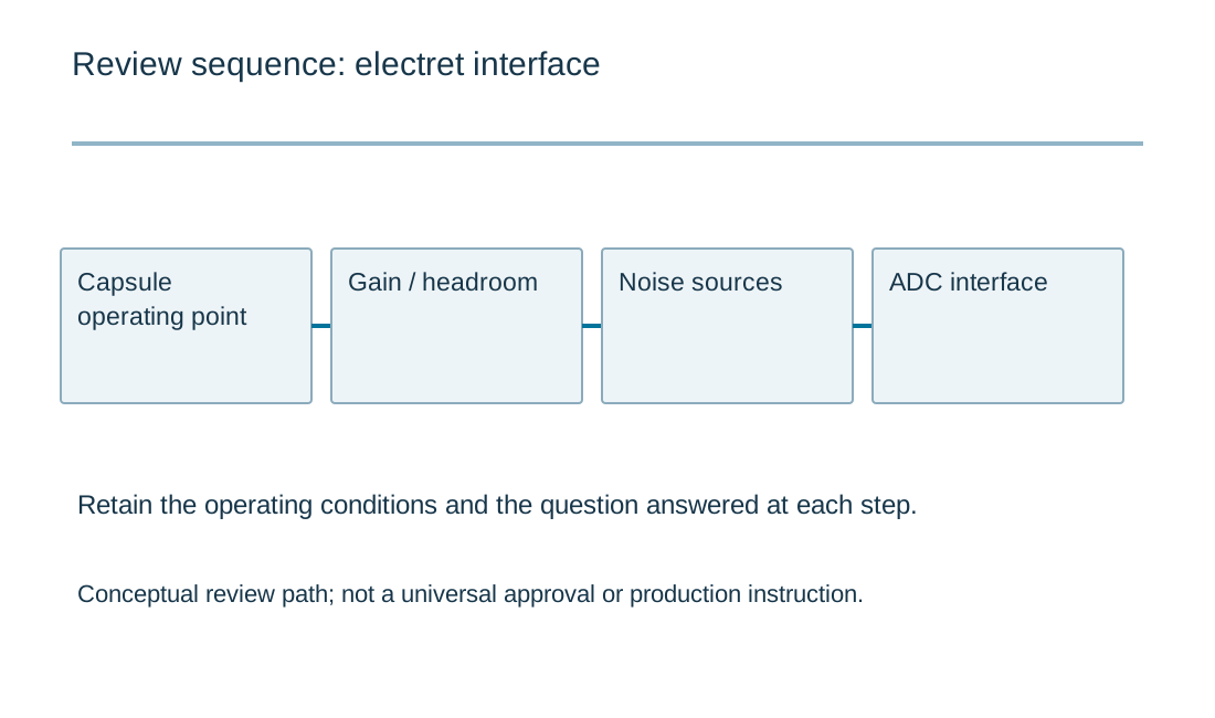
An electret microphone circuit supplies the capsule's internal electronics and extracts a small audio signal for amplification or conversion. Bias current, source impedance, coupling and noise all influence the result. A capsule that produces a signal is not necessarily operating at its intended point or using the available dynamic range well.
This guide covers a common two-wire capsule interface and its front-end PCB. It is separate from general power-amplifier design. The worksheet estimates a nominal bias condition and a simple coupling corner, making the assumptions visible before the actual capsule and amplifier circuit are evaluated.
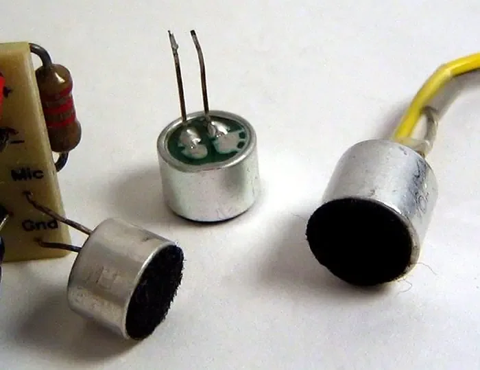
Identify the capsule rather than assuming a universal pinout
Use the exact capsule data for terminal assignment, permitted supply conditions, current and sensitivity. The metal case may have an electrical connection that matters to mounting and grounding. A mechanically similar capsule can have different electrical behavior or acoustic directionality. Do not identify terminals solely from a photograph of another part.
The internal field-effect-transistor arrangement of a typical two-wire electret capsule requires a suitable bias network. A resistor to a quiet supply establishes a load and operating condition, while the audio signal appears as a small variation around that point. The capsule is not an ideal fixed-voltage source, so its actual operating voltage should be established from data or measurement.
Specify the acoustic task: speech pickup, equipment sound, event detection or another use. Required bandwidth, signal level and environment influence the electrical design. A circuit optimized for one task may deliberately reject frequencies or levels important to another. Keep the acoustic requirement with the schematic rather than treating it as a later software problem.
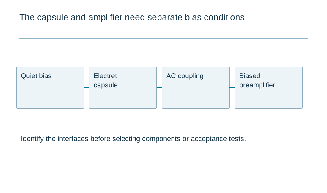
Estimate bias current at a declared operating point
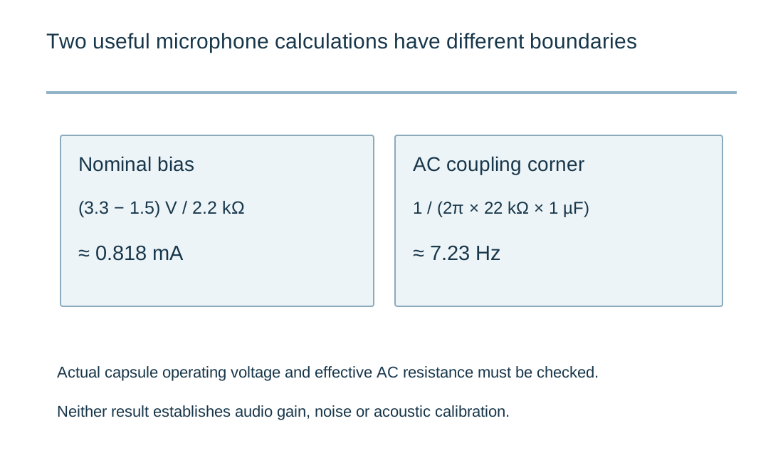
The worksheet uses the difference between bias supply and an assumed capsule operating voltage divided by the bias resistor. With 3.3 V supply, 1.5 V at the capsule and 2.2 kΩ, the resulting nominal current is about 0.818 mA. This is a circuit arithmetic example, not an automatically selected operating point for every capsule.
Check the actual capsule's allowed conditions and the load presented by the following stage. Supply ripple can enter the audio path through the bias network. Filtering may be useful, but the network's impedance and startup behavior should remain compatible with the required operation. Measure the capsule node under the intended conditions instead of assuming the entered voltage will appear.
The preamplifier input must tolerate the DC and AC conditions at its connection. A coupling capacitor can remove the capsule's DC level from the following bias arrangement, but it does not eliminate the need for a valid amplifier common-mode point. Review both sides of the capacitor in powered and unpowered states.
| Review item | What to establish |
|---|---|
| Capsule | Exact part, terminals, operating conditions and acoustic task. |
| Bias | Measured capsule point, quiet supply and permitted load. |
| Signal | Coupling, gain, clipping and ADC acquisition requirements. |
| Environment | Switching noise, vibration, airflow and enclosure geometry. |
| Evidence | Separate electrical injection, acoustic verification and calibration. |
Set coupling and gain from the whole signal chain
For a simplified capacitor feeding a resistive input, the high-pass corner is 1/(2πRC). A 1 µF capacitor and 22 kΩ load give about 7.23 Hz in that model. The actual effective resistance may include source impedance and additional bias paths. The tool therefore labels the result as a nominal first-order estimate rather than a complete measured frequency response.
Select gain with both quiet sounds and maximum expected input in mind. Too much gain can clip large signals or disturbances before software has a chance to process them. Too little gain can waste converter range and make downstream noise more significant. Account for amplifier output swing and ADC input requirements at the actual supply and load.
TI's TIPD181 is a primary reference example for an electret microphone preamplifier. Its design resources can help identify the kinds of bias, gain and measurement information required. Copying one resistor value from a reference does not reproduce its performance with a different capsule, supply or converter interface.
Electret bias and coupling estimate
Electret bias and coupling estimate
Use the current inputs and keep the assumptions
Load the example to inspect its units, then clear it before entering your own revision. Example values are deliberately labeled assumptions. Complete every field; an empty numeric input is not zero. Record the operating condition behind a value rather than copying the first number found on a component summary. For a comparison, keep the measurement boundary and units consistent.
Calculate after checking the inputs. Any edit invalidates the old result and disables its report download until you calculate again. An edited example remains identified as an example. Results and reports are generated locally without uploading a circuit or populating Contact. Attach the downloaded text manually if it helps explain the question. You can request a review directly without completing the tool.
| Input | What to establish before using it |
|---|---|
| Review reference | Nonconfidential revision label. |
| Bias supply · V | Quiet nominal supply. |
| Assumed capsule operating voltage · V | From actual capsule data or measurement; the capsule is not a fixed voltage source. |
| Bias resistor · kΩ | Between bias rail and two-wire capsule output. |
| AC input resistance · kΩ | Simplified resistive input load seen by the coupling capacitor. |
| Coupling capacitor · µF | First-order model; source impedance and bias network may change the effective resistance. |
Keep electrical noise distinct from acoustic noise
Route the low-level input away from switching nodes and digital edges where practical, with an appropriate return and shielding strategy for the installation. A long high-impedance trace can collect interference. At the same time, adding a ground area without considering capsule mounting or capacitive coupling may not solve the actual problem.
Regulators, clocks, displays and wireless activity can create repeatable artifacts. Test the audio path while those functions operate in representative modes. A quiet bench test with the processor idle may miss the disturbance heard during normal use. Preserve the operating state and spectrum or waveform when diagnosing the source.
Mechanical vibration and airflow can also produce microphone output. The acoustic opening, enclosure cavity and mounting material are part of the sensing system. Do not classify every low-frequency signal as electrical hum without checking the physical setup. A change to the enclosure can alter response while the PCB remains identical.
Design the ADC interface and data validity
If the signal enters an ADC, establish its input range, reference and acquisition requirements. The preamplifier may need to drive a sampling network rather than a simple resistor. Anti-alias filtering belongs to the relationship between analog bandwidth and sample rate; a coupling capacitor alone does not provide that low-pass function.
Keep clipping, startup settling and unavailable data identifiable in the processing chain. An amplitude number calculated from a saturated waveform can appear stable while being wrong. If sound level is reported in physical acoustic units, a suitable calibration and frequency-weighting method are required. Raw ADC counts or arbitrary software volume are not automatically sound-pressure level.
The PIR front-end guide also discusses filtering small sensor signals, but its temporal and optical requirements differ from audio. A photodiode front end uses a different current-to-voltage relationship. Share layout discipline where useful without transplanting one sensor's gain or filter assumptions into another.
Verify the finished interface and release it clearly
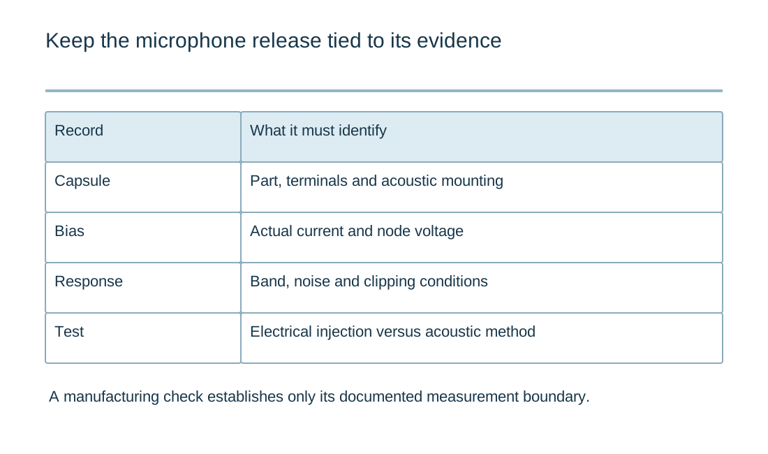
Measure DC bias, response over the intended band, clipping and noise under documented conditions. Use a repeatable acoustic or electrical stimulus appropriate to the test objective. Electrical injection can examine the amplifier path while bypassing the capsule and enclosure; an acoustic test includes those elements but needs a controlled source and geometry.
For manufacturing, supply the exact capsule, mounting orientation, acoustic opening and approved handling requirements. Identify the electrical checks, any calibration and the acceptance record required from the assembly supplier. A powered continuity or bias test should not be described as a complete microphone sensitivity verification.
Send RAYPCB the current schematic, board outputs, BOM and intended test boundary for a PCB or PCBA review. State whether the main concern is bias, noise, converter interface or mechanical integration. The local worksheet report can clarify assumptions, while the actual component documentation and measured response establish the design's suitability.
Validate the installed measurement chain
The sensor measures a local physical condition through a particular mounting and signal path. Its nominal resolution is not the accuracy of the installed system. Define the quantity, reference, useful response time and environment before deciding that a high-rate output or a long decimal value is meaningful.
Preserve raw observations, calibration coefficients and the conditions under which they were obtained. Check intermediate points and relevant environmental changes rather than only fitting endpoints. Separate invalid, stale and out-of-range data from valid low readings. Manufacturing tests should verify the electrical and assembly tasks actually agreed; field calibration and application validation need their own methods. Keep personal or confidential project details out of public worksheet labels and attach controlled records through the normal inquiry process.
Standards, source context and limits
Use the exact device revision and application conditions when applying manufacturer guidance. Reference designs are evidence about a specified implementation, not automatic validation of a modified board. Workmanship inspection, functional verification, product safety and application performance are different acceptance tasks. Public summaries do not replace the applicable licensed standards or a project-specific acceptance specification.
For fabrication scope and the agreed construction requirements, see PCB manufacturing.