In the ever-evolving world of digital electronics, Field-Programmable Gate Arrays (FPGAs) have become indispensable tools for designers seeking flexibility, performance, and efficiency. Among the various FPGA families available, the Xilinx Kintex-7 series stands out as a powerful and versatile option for a wide range of applications. This comprehensive guide delves into the Kintex-7 FPGA family, with a particular focus on three popular models: the XC7K325T, XC7K160T, and XC7K410T. We’ll explore their features, applications, and how they can be leveraged to create high-performance designs.
Understanding the Xilinx Kintex-7 FPGA Family
The Kintex-7 FPGA family, introduced by Xilinx, represents a significant advancement in FPGA technology. These devices are designed to deliver high performance and power efficiency, making them ideal for a variety of applications ranging from communications infrastructure to high-end consumer products.
Key Features of Kintex-7 FPGAs
28nm HPL (High-Performance, Low-Power) process technology
High-performance DSP slices for efficient signal processing
Flexible memory options, including block RAM and distributed RAM
Advanced clocking technology with low-jitter clock management
High-speed serial transceivers for efficient data transfer
Reduced power consumption compared to previous generations
The Kintex-7 Advantage
Kintex-7 FPGAs offer a balance between performance and cost, positioning themselves as an excellent choice for designers who need more capabilities than entry-level FPGAs but don’t require the extreme performance of high-end devices. This makes them particularly attractive for applications in telecommunications, medical imaging, and industrial automation.
Leveraging Kintex-7 FPGAs for High-Performance Designs
Now that we’ve explored the specifications of these Kintex-7 models, let’s discuss how to leverage their capabilities for high-performance designs.
Optimizing DSP Performance
Kintex-7 FPGAs feature advanced DSP slices that can significantly boost signal processing performance. To make the most of these resources:
Utilize DSP inference in your HDL code to ensure efficient mapping to DSP slices
Consider using Xilinx’s DSP IP cores for complex operations like FFTs and FIR filters
Implement pipelining to achieve higher clock frequencies and throughput
Efficient Memory Utilization
The Kintex-7 family offers various memory options, including block RAM and distributed RAM. To optimize memory usage:
Use block RAM for larger data storage requirements
Leverage distributed RAM for smaller, faster memory needs
Implement proper memory partitioning to avoid bottlenecks
Utilize Xilinx’s memory interface solutions for external memory connections
High-Speed I/O and Connectivity
The high-speed transceivers in Kintex-7 FPGAs enable efficient data transfer. To maximize their potential:
Implement proper signal integrity techniques for high-speed designs
Utilize Xilinx’s SelectIO technology for flexible I/O configurations
Consider using PCIe interfaces for high-bandwidth connectivity with host systems
Power Optimization Techniques
While Kintex-7 FPGAs are inherently power-efficient, further optimizations can be achieved:
Utilize clock gating to reduce dynamic power consumption
Implement power-aware placement and routing strategies
Use Xilinx’s Power Optimization tool to identify areas for improvement
Design Tools and Development Environment
Xilinx Kintex fpga
To effectively design with Kintex-7 FPGAs, it’s crucial to use the right tools and development environment.
Xilinx Vivado Design Suite
The primary development environment for Kintex-7 FPGAs is the Xilinx Vivado Design Suite. Key features include:
High-level synthesis for C/C++ to RTL conversion
Advanced timing analysis and optimization tools
Integrated logic analyzer for on-chip debugging
Power analysis and optimization capabilities
IP Cores and Reference Designs
Xilinx provides a wealth of IP cores and reference designs that can accelerate development with Kintex-7 FPGAs:
DSP IP cores for signal processing applications
Communication protocol cores (Ethernet, PCIe, etc.)
Memory interface solutions
Video and image processing IP
Third-Party Tools and Ecosystem
A robust ecosystem of third-party tools and IP providers further enhances the Kintex-7 design experience:
High-level synthesis tools from vendors like Mentor Graphics and Cadence
Specialized IP cores for specific applications
System-level design and verification tools
Real-World Applications and Case Studies
To better understand the capabilities of Kintex-7 FPGAs, let’s explore some real-world applications and case studies.
Case Study 1: 5G Base Station Design
A telecommunications company utilized the XC7K410T to develop a high-performance 5G base station. The abundant DSP resources allowed for efficient implementation of complex signal processing algorithms, while the high-speed transceivers enabled rapid data transfer between different system components.
Case Study 2: Medical Imaging Equipment
A medical device manufacturer leveraged the XC7K325T for a new generation of MRI scanners. The FPGA’s balanced resources allowed for real-time image processing and data acquisition, significantly improving image quality and reducing scan times.
Case Study 3: Industrial Automation
An industrial automation company used the XC7K160T to create a versatile control system for manufacturing plants. The FPGA’s compact size and ample resources enabled the implementation of complex control algorithms and multiple communication interfaces in a single device.
Future Trends and Developments
As technology continues to evolve, the role of FPGAs like the Kintex-7 series is likely to expand. Some future trends to watch include:
Increased integration of AI and machine learning capabilities
Enhanced support for edge computing applications
Further improvements in power efficiency and performance
Greater emphasis on security features and encryption
Conclusion
The Xilinx Kintex-7 FPGA family, particularly the XC7K325T, XC7K160T, and XC7K410T models, offers a powerful and flexible platform for high-performance designs across various industries. By understanding the unique features and capabilities of these devices, designers can leverage their potential to create innovative solutions that meet the demands of today’s complex applications.
Whether you’re working on telecommunications infrastructure, medical devices, industrial automation, or any other high-performance application, the Kintex-7 FPGA family provides the resources, performance, and efficiency needed to bring your designs to life. As the world of digital electronics continues to evolve, the Kintex-7 series stands ready to meet the challenges of tomorrow’s technologies.
In the world of embedded systems and electronics, PIC microcontrollers have become a cornerstone of innovation and development. These versatile chips, often referred to as PIC micros, PIC controllers, PIC MCUs, or PIC chips, have revolutionized the way we approach electronic design and automation.
What is a PIC Microcontroller?
A PIC microcontroller is a small, integrated circuit designed to perform specific tasks in embedded systems. PIC stands for Peripheral Interface Controller, which hints at its primary function – to control various peripherals and interfaces in electronic devices.
Brief History and Evolution
PIC microcontrollers were first introduced by Microchip Technology Inc. in the mid-1980s. Since then, they have undergone significant evolution, with each new generation bringing improvements in processing power, memory capacity, and peripheral features. Today, PIC microcontrollers are among the most widely used MCUs in the industry, powering everything from simple hobby projects to complex industrial systems.
Importance in Embedded System Design
The importance of PIC MCUs in embedded system design cannot be overstated. They offer a perfect balance of performance, cost-effectiveness, and versatility, making them suitable for a wide range of applications. From consumer electronics to automotive systems, PIC microcontrollers play a crucial role in bringing intelligence to everyday devices.
To fully appreciate the capabilities of PIC microcontrollers, it’s essential to understand their underlying architecture and the advantages it brings to embedded system design.
General Architecture of a PIC Processor
PIC microcontrollers are built on a solid architectural foundation that contributes to their efficiency and performance:
Harvard Architecture: PIC MCUs use a Harvard architecture, which separates program and data memory. This allows for simultaneous access to both instruction and data memory, enhancing overall performance.
RISC-based Design: PIC microcontrollers employ a Reduced Instruction Set Computing (RISC) architecture. This means they have a smaller set of instructions, each executed in a single clock cycle, leading to faster and more efficient processing.
Memory and Peripherals: A typical PIC microcontroller includes various types of memory:
Flash memory for program storage
EEPROM for non-volatile data storage
RAM for temporary data storage
Additionally, they feature a wide array of built-in peripherals such as timers, ADCs, PWM modules, and communication interfaces.
Advantages of PIC Microcontrollers
PIC microcontrollers offer several advantages that have contributed to their widespread adoption:
Cost-effective: PIC MCUs provide a high level of functionality at a relatively low cost, making them accessible for both hobbyists and large-scale industrial applications.
Low Power Consumption: Many PIC microcontrollers are designed with power efficiency in mind, making them ideal for battery-operated and energy-conscious applications.
Wide Availability: With a vast range of models catering to different needs, PIC microcontrollers are readily available, ensuring that developers can find the right chip for their specific requirements.
Robust Ecosystem: PIC microcontrollers benefit from a mature ecosystem of development tools, software libraries, and community support, making development easier and more efficient.
III. Key Families of PIC Microcontrollers
Microchip Technology offers a diverse range of PIC microcontrollers, each tailored to specific application needs. Let’s explore some of the key families:
A. PIC16 Series (8-bit)
The PIC16 series represents the backbone of 8-bit PIC microcontrollers, offering a perfect balance of performance and affordability. Within this series, the PIC16F877A stands out as one of the most popular and versatile options.
Focus on the PIC16F877A Microcontroller
The PIC16F877A has become a favorite among hobbyists and professionals alike due to its rich feature set and ease of use. Let’s delve into its key features:
8-bit RISC Architecture: The PIC16F877A uses an efficient 8-bit RISC core, allowing for fast execution of instructions.
Memory: It offers 368 bytes of RAM and 256 bytes of EEPROM, providing ample space for data storage and program memory.
I/O and Peripherals: With 33 I/O pins and 5 channels of 10-bit Analog-to-Digital Converters (ADC), the PIC16F877A is well-equipped for interfacing with various sensors and actuators.
Communication Interfaces: It supports multiple communication protocols, including USART, SPI, and I²C, facilitating easy integration with other devices.
Timer Modules: The PIC16F877A includes several timer modules, enabling precise timing control in applications.
Use Cases for PIC16F877A
The PIC16F877A finds applications in a wide range of projects, including:
Robotics: Controlling motors, sensors, and decision-making logic
Home Automation: Managing lighting, temperature control, and security systems
Educational Projects: Serving as an excellent platform for learning microcontroller programming
Industrial Control: Monitoring and controlling industrial processes
B. PIC18 Series (Advanced 8-bit)
The PIC18 series represents an evolution of the 8-bit PIC architecture, offering enhanced performance and additional features compared to the PIC16 series.
Key Features of PIC18 Microcontrollers
Improved Performance: PIC18 MCUs offer higher clock speeds, typically ranging from 40 MHz to 64 MHz, allowing for faster execution of instructions.
Enhanced Peripheral Set: These microcontrollers come with an expanded set of peripherals, including more advanced timer modules, enhanced PWM capabilities, and improved communication interfaces.
Larger Memory: PIC18 series offers increased program and data memory, supporting more complex applications.
C Compiler Optimized: The architecture is optimized for C language programming, making it easier to develop complex applications using high-level languages.
Applications of PIC18 Series
PIC18 microcontrollers are commonly used in:
Automotive Systems: Engine control units, body electronics, and infotainment systems
Industrial Control: PLC systems, motor control, and process automation
Consumer Electronics: Appliances, remote controls, and smart home devices
Medical Devices: Patient monitoring equipment and portable diagnostic tools
C. dsPIC30/dsPIC33 (16-bit Digital Signal Controllers)
The dsPIC series, particularly the dsPIC33, represents Microchip’s venture into the world of Digital Signal Controllers (DSCs). These devices combine the features of a microcontroller with the signal processing capabilities of a Digital Signal Processor (DSP).
Key Features of dsPIC33
16-bit Architecture: The dsPIC33 uses a 16-bit core, offering higher processing power compared to 8-bit PICs.
DSP Capabilities: It includes hardware multipliers and accumulators for efficient digital signal processing operations.
High-Speed Operation: Many dsPIC33 models can operate at clock speeds up to 150 MHz, enabling real-time processing of complex algorithms.
Advanced Peripherals: dsPIC33 controllers often include specialized peripherals for motor control, power conversion, and high-speed communication.
Applications of dsPIC33
The dsPIC33 family is particularly well-suited for applications requiring both microcontroller functionality and signal processing capabilities:
Motor Control: Precise control of electric motors in industrial and automotive applications
Power Conversion: Digital power supplies and inverters
Audio Processing: Digital audio effects and sound processing in consumer electronics
Sensor Fusion: Combining data from multiple sensors in IoT and automotive applications
IV. Tools and Software for PIC Development
Developing applications for PIC microcontrollers requires a set of specialized tools and software. Microchip Technology provides a comprehensive ecosystem to support PIC development:
Popular PIC Programmers
PICkit: A series of low-cost programmers ideal for hobbyists and small-scale development. The latest version, PICkit 4, offers support for a wide range of PIC and dsPIC devices.
MPLAB ICD (In-Circuit Debugger): A more advanced tool that allows for programming and real-time debugging of PIC microcontrollers.
MPLAB REAL ICE: A high-end in-circuit emulator for professional development, offering advanced debugging capabilities.
MPLAB X IDE and XC Compilers
MPLAB X IDE: Microchip’s free, open-source Integrated Development Environment (IDE) for PIC development. It provides a user-friendly interface for writing, debugging, and managing projects.
XC Compilers: A suite of C compilers optimized for different PIC families:
XC8 for 8-bit PICs
XC16 for 16-bit PICs and dsPICs
XC32 for 32-bit PICs
Simulators and Debuggers
MPLAB Simulator: An integrated simulator within MPLAB X IDE, allowing developers to test code without physical hardware.
Proteus: A popular third-party simulation software that supports various PIC microcontrollers and allows for virtual circuit design and testing.
Tips for PIC Microcontroller Programming
Start with simple projects to familiarize yourself with the PIC architecture and development environment.
Make use of Microchip’s extensive documentation and application notes.
Utilize built-in peripherals whenever possible to optimize code efficiency.
Implement proper debouncing techniques when working with buttons or switches.
Use interrupt-driven programming for time-critical tasks.
V. Applications of PIC Microcontrollers
PIC microcontrollers have found their way into numerous applications across various industries. Their versatility, cost-effectiveness, and robust feature set make them suitable for a wide range of projects:
Consumer Electronics
Remote Controls: Many TV, air conditioning, and other appliance remotes use PIC microcontrollers for their operation.
Smart Home Devices: PIC MCUs power various IoT devices, from smart switches to environmental sensors.
Digital Clocks and Timers: PIC16 series chips are often used in digital clock applications.
Medical Devices
Blood Glucose Meters: PIC microcontrollers handle the data processing and display in portable glucose monitoring devices.
Digital Thermometers: PIC chips manage temperature sensing and display in digital thermometers.
Pulse Oximeters: PIC18 or dsPIC33 controllers process signals from optical sensors in these devices.
For those new to PIC microcontrollers, getting started can be an exciting journey. Here’s a guide to help you set up your development environment and create your first PIC project:
Setting Up a Development Environment
Installing MPLAB X IDE:
Visit the Microchip website and download the latest version of MPLAB X IDE.
Follow the installation wizard to complete the setup.
Install the appropriate XC compiler for your PIC family (XC8 for 8-bit PICs, XC16 for 16-bit PICs).
Choosing a PIC Board: For beginners, it’s recommended to start with a development board. The PIC16F877A development board is an excellent choice due to its versatility and extensive documentation.
Writing Your First Program (Blinking LED Example)
Let’s create a simple program to blink an LED using a PIC16F877A:
 #include <xc.h>
#include <stdint.h>

// Configuration bits
#pragma config FOSC = HS        // Oscillator Selection bits (HS oscillator)
#pragma config WDTE = OFF       // Watchdog Timer Enable bit (WDT disabled)
#pragma config PWRTE = OFF      // Power-up Timer Enable bit (PWRT disabled)
#pragma config BOREN = ON       // Brown-out Reset Enable bit (BOR enabled)
#pragma config LVP = OFF        // Low-Voltage (Single-Supply) In-Circuit Serial Programming Enable bit (RB3 is digital I/O, HV on MCLR must be used for programming)
#pragma config CPD = OFF        // Data EEPROM Memory Code Protection bit (Data EEPROM code protection off)
#pragma config WRT = OFF        // Flash Program Memory Write Enable bits (Write protection off; all program memory may be written to by EECON control)
#pragma config CP = OFF         // Flash Program Memory Code Protection bit (Code protection off)

#define _XTAL_FREQ 20000000     // 20 MHz oscillator

void main(void) {
    TRISB0 = 0;                 // Set RB0 as output

    while(1) {
        RB0 = 1;                // Turn LED on
        __delay_ms(500);        // Wait for 500 ms
        RB0 = 0;                // Turn LED off
        __delay_ms(500);        // Wait for 500 ms
    }
}
This program will cause an LED connected to pin RB0 to blink every second.
Programming the PIC Microcontroller
Connect your PIC programmer (e.g., PICkit) to your computer and the development board.
In MPLAB X IDE, create a new project and select your PIC model (PIC16F877A in this case).
Copy the above code into the main source file.
Build the project and program the PIC using the “Make and Program Device” option in MPLAB X IDE.
Congratulations! You’ve just programmed your first PIC microcontroller. This simple example demonstrates the basics of PIC programming, including port configuration, digital output, and timing delays.
VII. Choosing the Right PIC MCU for Your Project
Selecting the appropriate PIC microcontroller for your project is crucial for its success. Here are some factors to consider:
Factors to Consider
Memory and Speed Requirements:
Assess the amount of program memory and RAM your application needs.
Determine the processing speed required for your tasks.
Peripheral Support:
List the peripherals your project requires (e.g., ADC, UART, I2C, SPI).
Check if the MCU has the necessary number of I/O pins.
Voltage and Power Considerations:
Determine the operating voltage of your system.
Consider power consumption, especially for battery-operated devices.
Cost and Availability:
Balance the features you need with your budget constraints.
Ensure long-term availability for production projects.
Comparison Table: PIC16F877A vs PIC18F vs dsPIC33
Feature
PIC16F877A
PIC18F452
dsPIC33FJ128GP802
Architecture
8-bit
8-bit
16-bit
Max Clock Speed
20 MHz
40 MHz
80 MHz
Program Memory
8K x 14 words
32K x 16 words
128K x 24 words
RAM
368 bytes
1536 bytes
16K bytes
EEPROM
256 bytes
256 bytes
None
ADC
10-bit, 8 channels
10-bit, 8 channels
12-bit, 9 channels
I/O Pins
33
34
28
UART
1
1
2
SPI/I2C
Yes
Yes
Yes
PWM
2 channels
2 channels
6 channels
DSP Capabilities
No
No
Yes
Typical Use Case
General Purpose
Advanced 8-bit
Motor Control, DSP
This comparison illustrates the progression in capabilities from the 8-bit PIC16F877A to the more advanced 8-bit PIC18F452, and finally to the 16-bit dsPIC33FJ128GP802 with its enhanced processing power and DSP features.
VIII. Tips and Resources for PIC Enthusiasts
To help you on your journey with PIC microcontrollers, here are some valuable tips and resources:
Forums, Books, and Communities
Microchip Forums: The official Microchip forums are an excellent place to ask questions and share knowledge with other PIC developers.
Books:
“PIC Microcontrollers: Know It All” by Lucio Di Jasio
“Programming 8-bit PIC Microcontrollers in C” by Martin P. Bates
“Designing Embedded Systems with PIC Microcontrollers” by Tim Wilmshurst
Online Communities:
Stack Overflow’s [pic] tag
Reddit’s r/PIC_Programming subreddit
EEVblog Forum’s Microcontrollers section
Recommended Starter Kits
PICkit 3 Starter Kit: Includes a PICkit 3 programmer/debugger and a development board with various peripherals.
PIC18F Starter Kit: A more advanced kit featuring a PIC18F46K22 MCU and multiple sensors and interfaces.
dsPIC33 Motor Control Starter Kit: Ideal for those interested in motor control applications using dsPIC33 controllers.
Best Practices in PIC Microcontroller Design and Programming
Use Timer Interrupts: For precise timing, rely on timer interrupts rather than delay loops.
Implement Proper Debouncing: When using buttons or switches, implement software debouncing to prevent false triggers.
Optimize Power Consumption: Utilize sleep modes and peripheral management to reduce power usage in battery-operated devices.
Comment Your Code: Maintain clear and comprehensive comments in your code for easier maintenance and collaboration.
Leverage Built-in Peripherals: Make use of built-in hardware peripherals whenever possible to offload tasks from the CPU.
Keep Up with Documentation: Regularly refer to datasheets and errata to stay informed about device-specific features and limitations.
IX. Conclusion
The world of PIC microcontrollers offers a vast playground for both hobbyists and professionals in the field of embedded systems. From the versatile 8-bit PIC16F877A to the powerful 16-bit dsPIC33 series, these microcontrollers provide a scalable platform for a wide range of applications.
The PIC family’s strength lies in its diversity, offering solutions for simple control tasks to complex signal processing applications. Whether you’re building a home automation system with a PIC16F, developing an industrial controller with a PIC18F, or designing a high-performance motor control system with a dsPIC33, there’s a PIC microcontroller suited for your needs.
As we’ve explored throughout this guide, the ecosystem surrounding PIC microcontrollers is rich with development tools, resources, and community support. This comprehensive environment makes PIC MCUs an excellent choice for both learning and professional development.
We encourage you to explore the capabilities of PIC microcontrollers hands-on. Start with simple projects, gradually increase complexity, and don’t hesitate to experiment with different PIC families. The skills and knowledge you gain will be invaluable in the ever-evolving world of embedded systems and IoT.
Remember, the journey of mastering PIC microcontrollers is ongoing. Stay curious, keep learning, and most importantly, enjoy the process of bringing your ideas to life with these powerful little chips!
X. FAQ (for Featured Snippets and SEO Boost)
What is the difference between PIC and other microcontrollers? PIC microcontrollers use a Harvard architecture and RISC instruction set, offering efficiency and speed. They are known for their wide range of options, from simple 8-bit to advanced 16-bit DSC models, and have a mature ecosystem of development tools.
What is PIC16F877A used for? The PIC16F877A is a versatile 8-bit microcontroller commonly used in hobbyist projects, educational settings, and simple industrial applications. It’s popular for tasks like motor control, sensor interfacing, and basic automation due to its balance of features and affordability.
How do I program a PIC chip? To program a PIC chip, you need:
A PIC programmer (like PICkit)
MPLAB X IDE and appropriate XC compiler
Write your code in C or assembly
Compile the code and use the programmer to flash it onto the PIC chip
Is dsPIC the same as PIC? dsPIC is a subfamily of PIC microcontrollers. While regular PICs are general-purpose microcontrollers, dsPICs are Digital Signal Controllers that combine microcontroller features with Digital Signal Processing capabilities, making them suitable for more complex signal processing tasks.
What is the best PIC programmer for beginners? The PICkit 3 or PICkit 4 is often recommended for beginners. These programmers are affordable, easy to use, and support a wide range of PIC microcontrollers. They also integrate well with Microchip’s MPLAB X IDE, providing a smooth development experience for newcomers.
In the ever-evolving world of electronics and computing, two terms often come up in discussions about smart devices and embedded systems: microcontrollers and microprocessors. While both play crucial roles in modern technology, they serve different purposes and have distinct characteristics. In this comprehensive guide, we’ll compare microcontroller vs. microprocessor to highlight their key differences and real-world applications, helping you understand when and where to use each technology.
Whether you’re a budding engineer, a curious hobbyist, or a professional looking to make informed decisions about component selection, understanding the nuances between these two technologies is essential. Let’s dive into the world of microcontrollers and microprocessors, exploring their unique features, strengths, and ideal use cases.
A microcontroller, often abbreviated as MCU (Microcontroller Unit), is a small computer on a single integrated circuit. It’s designed to be a compact, self-contained system for controlling specific operations in embedded systems. Think of it as a tiny, specialized computer that’s optimized for specific tasks rather than general-purpose computing.
Architecture of a Microcontroller
The architecture of a microcontroller is what sets it apart from other computing devices. A typical microcontroller includes:
CPU (Central Processing Unit): The brain of the microcontroller, responsible for executing instructions.
Memory: Both RAM (Random Access Memory) for temporary data storage and ROM (Read-Only Memory) or flash memory for storing the program code.
I/O (Input/Output) Ports: For interfacing with external devices and sensors.
Peripherals: Built-in hardware like timers, ADCs (Analog-to-Digital Converters), and communication interfaces (UART, SPI, I2C, etc.).
All these components are integrated into a single chip, making microcontrollers compact and energy-efficient.
Common Features of Microcontrollers
Microcontrollers are known for several key features that make them ideal for embedded applications:
Low Power Consumption: Designed to operate efficiently in battery-powered devices.
Compact Size: Ideal for small, space-constrained applications.
Built-in Timers and Counters: For precise timing and event counting without external components.
Integrated ADCs and DACs: For interfacing with analog sensors and actuators.
Multiple I/O Ports: Enabling easy connection to various external devices.
Real-Time Capabilities: Suitable for applications requiring immediate response to events.
Examples of Microcontrollers
Some popular microcontrollers include:
Arduino: A family of microcontroller boards widely used in hobbyist and educational projects.
STM32: ARM Cortex-M based microcontrollers from STMicroelectronics, known for their performance and versatility.
ATmega328: The microcontroller used in many Arduino boards, known for its simplicity and ease of use.
PIC Microcontrollers: A series of microcontrollers made by Microchip Technology, popular in industrial applications.
What is a Microprocessor?
Definition and Core Concept
A microprocessor, often simply called a processor, is a more complex and powerful computing unit compared to a microcontroller. It’s the central processing unit (CPU) of a computer system, designed to perform general-purpose computing tasks. Unlike microcontrollers, microprocessors typically require additional external components to form a complete computer system.
Microprocessor Architecture
The architecture of a microprocessor differs significantly from that of a microcontroller:
CPU: The microprocessor itself is essentially just the CPU, containing the arithmetic logic unit (ALU), control unit, and registers.
External Memory: Requires separate RAM and ROM chips for program and data storage.
I/O Interfaces: Needs external chips to handle input/output operations.
Peripherals: Generally lacks built-in peripherals, relying on separate chips for additional functionality.
This modular approach allows for more flexibility and power but results in larger, more complex systems.
Key Characteristics of Microprocessors
Microprocessors are distinguished by several important features:
High Processing Power: Capable of handling complex computations and multitasking.
Flexibility: Can be used for a wide range of computing tasks.
Scalability: Easy to upgrade or expand system capabilities.
Advanced Instruction Sets: Support for complex operations and programming paradigms.
Higher Clock Speeds: Generally operate at much higher frequencies than microcontrollers.
Examples of Microprocessors
Some well-known microprocessors include:
Intel Core Series: Popular in desktop and laptop computers (e.g., Intel Core i7, i9).
AMD Ryzen: Competitive high-performance processors for personal computers.
ARM Cortex-A Series: Widely used in smartphones and tablets.
IBM POWER: Used in servers and high-performance computing systems.
Microcontroller vs. Microprocessor: Key Differences
Understanding the differences between microcontrollers and microprocessors is crucial for selecting the right component for your project. Let’s break down the key distinctions in a comprehensive comparison table:
Feature
Microcontroller
Microprocessor
Architecture
All-in-one (CPU, memory, I/O)
CPU only, requires external components
Power Consumption
Low
High
Cost
Generally inexpensive
More expensive
Size
Small, suitable for embedded systems
Larger systems
Performance
Lower processing power
High-speed computing
Memory
Limited on-chip memory
Expandable external memory
I/O Capabilities
Built-in, specialized
Requires external interfaces
Instruction Set
Often simplified, application-specific
Complex, general-purpose
Interrupt Handling
Fast, suited for real-time applications
Can be slower due to complex architecture
Multitasking
Limited
Extensive
Development Tools
Often proprietary, specific to the microcontroller
Widely available, standardized
Applications
Real-time embedded tasks
Complex computational tasks
Customization
Limited, fixed hardware configuration
Highly customizable with external components
Boot Time
Near-instantaneous
Longer boot process
Operating System
Often runs without an OS or with a simple RTOS
Requires a full-fledged OS (e.g., Windows, Linux)
This comparison highlights the fundamental differences between microcontroller and microprocessor architectures and capabilities. The choice between them often comes down to the specific requirements of the project at hand.
When to Use a Microcontroller
Microcontrollers excel in specific scenarios where their unique characteristics provide significant advantages. Here are some key application areas and reasons to choose a microcontroller:
1. IoT Devices
Internet of Things (IoT) devices often require low power consumption, small form factor, and the ability to interface with various sensors. Microcontrollers are ideal for:
Smart home devices (thermostats, lighting controls)
Wearable fitness trackers
Environmental monitoring sensors
2. Home Automation
In home automation systems, microcontrollers can efficiently control various aspects of a smart home:
Automated blinds and curtains
Smart door locks
Irrigation systems
3. Wearables
The compact size and low power consumption of microcontrollers make them perfect for wearable technology:
Smartwatches
Health monitoring devices
AR/VR controllers
4. Automotive Electronics
Modern vehicles incorporate numerous microcontrollers for various functions:
Engine control units (ECUs)
Anti-lock braking systems (ABS)
Climate control systems
5. Industrial Control Systems
In industrial settings, microcontrollers are used for precise control and monitoring:
Microcontrollers offer several advantages in embedded system design:
Real-Time Performance: Quick response to inputs and interrupts.
Reliability: Simplified architecture leads to fewer points of failure.
Cost-Effectiveness: Lower component count reduces overall system cost.
Energy Efficiency: Ideal for battery-operated or energy-harvesting systems.
Compact Design: Allows for miniaturization of devices.
When to Use a Microprocessor
Microprocessors are the powerhouses of computing, designed for scenarios that require high performance and flexibility. Here are some key applications and reasons to opt for a microprocessor:
1. Personal Computers
The most common application of microprocessors is in personal computers:
Desktop computers
Laptops and notebooks
All-in-one PCs
2. Smartphones
Modern smartphones rely on powerful microprocessors to handle diverse tasks:
Running complex mobile operating systems (iOS, Android)
High-speed data acquisition and processing systems
5. Gaming Consoles
Modern gaming systems use powerful microprocessors to deliver immersive experiences:
PlayStation and Xbox consoles
High-end gaming PCs
Advantages of Microprocessors
Microprocessors offer several benefits in these applications:
High Processing Power: Ability to handle complex calculations and data processing.
Multitasking Capabilities: Can run multiple applications simultaneously.
Scalability: Easy to upgrade or expand system capabilities.
Flexibility: Can be programmed for a wide variety of tasks.
Advanced Features: Support for technologies like virtualization and advanced security features.
How to Choose: Microcontroller or Microprocessor?
Selecting between a microcontroller and a microprocessor depends on various factors. Here’s a decision-making guide to help you choose the right component for your project:
Decision Factors
Cost and Size Constraints
Limited budget or space? → Consider a microcontroller
Larger budget and space available? → A microprocessor might be suitable
Power Availability
Battery-operated or low-power requirement? → Microcontroller
Access to continuous power supply? → Microprocessor is an option
Performance Needs
Simple, dedicated tasks? → Microcontroller
Complex computations or multitasking? → Microprocessor
Peripheral Requirements
Need built-in peripherals (ADC, timers, etc.)? → Microcontroller
Require flexibility in peripheral selection? → Microprocessor
Non-time-critical applications? → Microprocessor can work
Development Complexity
Simple, focused application? → Microcontroller
Complex software with OS requirements? → Microprocessor
Scalability and Future Expansion
Fixed, specific functionality? → Microcontroller
Potential for significant expansion? → Microprocessor
Decision Flowchart
To simplify the decision-making process, consider the following flowchart:
Start
Is the application battery-powered or requires low energy consumption?
Yes → Lean towards Microcontroller
No → Continue
Does the application require complex computations or heavy multitasking?
Yes → Lean towards Microprocessor
No → Continue
Is real-time response critical?
Yes → Lean towards Microcontroller
No → Continue
Are built-in peripherals (ADC, timers, etc.) necessary?
Yes → Lean towards Microcontroller
No → Continue
Is the application space-constrained?
Yes → Lean towards Microcontroller
No → Consider Microprocessor
End
Remember, this flowchart is a general guide. Some applications may have unique requirements that don’t fit neatly into these categories.
Future Trends
The landscape of microcontrollers and microprocessors is continuously evolving. Let’s explore some emerging trends and future directions:
1. System on Chip (SoC)
SoCs are blending features of both microcontrollers and microprocessors:
Integrating powerful processors with microcontroller-like peripherals
Examples: Apple M1, Qualcomm Snapdragon series
Enabling more powerful, yet energy-efficient devices
2. AI and Machine Learning Integration
Both microcontrollers and microprocessors are adapting to support AI:
Microcontrollers with built-in neural processing units for edge AI
Microprocessors with dedicated AI accelerators
Enabling local processing for IoT and smart devices
3. Edge Computing
The rise of edge computing is influencing chip design:
More powerful microcontrollers for local data processing
Energy-efficient microprocessors for edge servers
Reducing latency and bandwidth requirements in IoT ecosystems
4. Advanced Manufacturing Processes
Continued advancements in semiconductor manufacturing are impacting both technologies:
Smaller process nodes (5nm, 3nm, and beyond)
Increased energy efficiency and performance
3D chip stacking and advanced packaging techniques
5. Specialized Architectures
We’re seeing a trend towards more specialized chip designs:
Domain-specific architectures for AI, graphics, cryptography
Quantum computing integration with classical processors
Neuromorphic computing mimicking brain functions
6. Security Enhancements
With increasing concerns about cybersecurity:
Built-in security features in both microcontrollers and microprocessors
Hardware-level encryption and secure boot capabilities
Trusted execution environments becoming standard
As these trends continue to develop, the line between microcontrollers and microprocessors may blur further, leading to more versatile and powerful computing solutions for a wide range of applications.
Conclusion
In the microcontroller vs. microprocessor debate, there’s no universal winner. Each technology has its strengths and ideal applications. Microcontrollers excel in embedded systems where size, power efficiency, and real-time performance are crucial. They’re the go-to choice for IoT devices, wearables, and many industrial control applications.
On the other hand, microprocessors shine in scenarios requiring high processing power, flexibility, and complex computations. They form the heart of our personal computers, smartphones, and servers, driving the digital world we live in.
The choice between a microcontroller and a microprocessor ultimately depends on your specific project requirements. Consider factors like power consumption, processing needs, size constraints, and development complexity when making your decision.
As technology advances, we’re seeing exciting developments like System on Chip (SoC) designs that blend features of both worlds, and specialized architectures optimized for AI and edge computing. These innovations promise to open up new possibilities in computing and embedded systems.
Whether you’re developing the next smart home device, designing an industrial control system, or building a high-performance computing application, understanding the strengths and limitations of microcontrollers and microprocessors is key to making informed decisions. By choosing the right technology for your needs, you can optimize your design for performance, efficiency, and cost-effectiveness.
Frequently Asked Questions (FAQ)
1. What is the main difference between a microcontroller and a microprocessor?
The main difference lies in their architecture and purpose. A microcontroller is a self-contained system with a processor, memory, and peripherals all on a single chip, designed for specific tasks in embedded systems. A microprocessor, on the other hand, is primarily just a CPU, requiring external components for memory and I/O, and is designed for general-purpose computing tasks.
2. Which is better: microcontroller or microprocessor?
Neither is universally “better” – it depends on the application. Microcontrollers are better for embedded systems, IoT devices, and applications requiring low power consumption and real-time performance. Microprocessors are superior for complex computing tasks, multitasking, and applications requiring high processing power.
3. Can a microcontroller replace a microprocessor?
In some cases, yes, especially with the advent of more powerful microcontrollers. However, for applications requiring high processing power or complex operating systems, a microprocessor is still
Counterfeit electronic components are a major issue facing the electronics supply chain. Unknowingly using fake or substandard parts can jeopardize product quality, reliability, and safety. Unfortunately, counterfeits have infiltrated authorized distributor channels and even original component manufacturers (OCMs). Combating counterfeits requires diligence across organizations involved in sourcing, procurement, quality control, and production. This article provides guidance on detecting counterfeit electronic components to aid in keeping them out of your supply chain.
How Counterfeits Enter the Supply Chain
To protect against counterfeits, it’s important to understand how they infiltrate the electronics ecosystem. Common paths include:
Independent distributors – Unscrupulous brokers re-sell used, recycled, remarked, or outright fake components acquired through various means.
Contract manufacturers – Some CM’s cut costs by quietly sourcing from unauthorized channels susceptible to fakes.
Online marketplaces – Counterfeiters leverage sites like Alibaba and eBay with little oversight on authenticity.
Phony franchises or manufacturers – Imposter operations pose as authorized sources and sell remarketed or fake parts.
Recycled materials – Legally recycled e-waste can get unlawfully mixed into new stock.
Theft and remarking – Components rejected or scrapped by OCMs get stolen and resold as new.
While motivations and sources vary, the common thread is introducing counterfeit components into supply chains that lack adequate screening processes.
Require suppliers provide detailed test reports from independent labs proving parts meet OEM specifications.
Contractual Obligations
Bind suppliers to contracts requiring:
Notification if any indication parts may be counterfeit or at risk
Certificates of Conformance with accompanying documentation
Indemnification against financial damages from supplying fakes
Right to conduct unannounced audits of facilities, processes, and inventory
Access to traceability and anti-counterfeit records
Anti-Counterfeit Technologies
Some OCMs are adopting emerging tech like blockchain, smart tags, and DNA marking to track, authenticate, and confirm component provenance throughout the supply chain. Require use of these protections whenever possible.
For less critical commercial goods, these measures may be prohibitive. But when lives depend on it, it’s worth the extra diligence and cost.
Conclusion
While counterfeit components continue infiltrating electronics supply chains, taking proper precautions can greatly reduce your organization’s risk. By partnering only with certified, authorized sources, inspecting diligently, and integrating robust counterfeit avoidance practices across procurement, logistics, quality control, and production you can safeguard product integrity. With growing threats from fake parts, enacting comprehensive anti-counterfeiting measures is a wise investment.
Frequently Asked Questions
Q: How extensive of an issue are counterfeit electronic components?
Counterfeit electronic components have grown into a massive issue, with some estimates indicating up to 10% of parts procured from independent distributors are fake. This problem has mushroomed as global supply chains have become more complex. The impact of counterfeit parts can undermine product integrity on a large scale once they enter global distribution channels.
Q: What are some warning signs a supplier may not be trustworthy?
Red flags include reluctance to provide requested documentation like certificates of conformance, audit rights, and test reports. Lack of industry certifications, evasive answers, unusual payment terms, prices that seem too good to be true, vague company ownership, and other shady attributes also warrant further scrutiny of a supplier’s authenticity.
Q: Is it safe to use components purchased from online marketplaces like Alibaba and eBay?
Generally it is risky and not advisable to source electronic components through online marketplaces. These platforms lack oversight to ensure authentic, authorized parts. The prevalence of counterfeits from such marketplaces makes it an unreliable sourcing channel for anything beyond hobbyist or experimental use. For production applications, only trusted franchised sources should be used.
Q: Can visual inspection reliably detect all counterfeit parts?
While valuable, visual inspection alone is not sufficient in many cases. High quality counterfeits may superficially look identical to authentic parts. More advanced techniques like x-ray imaging, sample destructive testing, electrical parameter validation, and supply chain auditing is often required to reliably weed out sophisticated fakes. The right combination of inspection methods and supply chain controls is needed.
Q: What liabilities can arise from using counterfeit electronic components?
Knowingly or negligently sourcing and installing counterfeit parts in shipping products can open companies up to significant legal liabilities. Product liability lawsuits, regulatory fines, and breach of warranty costs can occur if counterfeits cause systems to malfunction, fail prematurely, or result in other damages. It is imperative to demonstrate reasonable efforts were taken to prevent infiltration of fakes.
Farewell to Counterfeit Electronic Components
Everything that is made on earth by humans has a specific life that it works, after that, this product starts to decay or degrade in performance and in the end it may totally collapse or become obsolete. The designers of that product either it be mechanical or electrical takes numerous parameters into consideration to enhance the life time of that product. So these types of electronic items those which have completed their time and become obsolete or have become faulty, or out dated or damaged and become non-repairable will be thrown as “scrap items”. These scrap electronics is what contributes to e-waste. The business of scrap and e-waste is a very big industry or multibillion dollar industry.
There are countless electronic products that are being scrapped on daily basis throughout the world and this scrap or e-waste is being bought and sold at various prices. Mostly the e-waste or scrap is exported from the USA to China and other countries where it is washed in polluted water of river and then put on sideways to dry up. After that it is then forged by numerous ways like sanding, painting and applying false marks to make it look new. Hence we can say that the biggest source of the counterfeit components is the e-waste or scrap electronic market itself. It is the responsibility of the governments to devise a strategy to properly dispose of e-waste and scrap electronics so that it may not be accessible to “counterfeiters”
Many of us might have gone through some electronics parts to be used in hobby projects. Let’s say a 555 timer IC is used in an A-stable multi-vibrator circuit. Now the circuit is developed on breadboard and all the wire connections are intact. Power supply is good and you just turned ON your circuit and put oscilloscope at the output of 555 timer IC but you did not get the waveform. You then checked the oscilloscope settings and found perfectly fine. Now you start to think why my output is not coming, because you have blind believe in IC that it has no problem. You are constantly looking errors in your connections, breadboard, oscilloscope and other passive components, then after struggling half or one hour you realize that the IC itself is “counterfeit” or “fake”. So what happened in the process is the complete waste of your time, money and effort. This what counterfeit components do..!
A counterfeit component is the low quality, faulty and underrated component that is disguised as high quality or new component and it does not perform function correctly or malfunction causing problems for end users or buyers.
Why Counterfeit Electronic Components are made..?
Now that we understand what is counterfeit electronic components and from where mostly they emerge. As for the reason why they exist in markets is the simple reason “Money”. Yes, it has been estimated that this counterfeit electronic components industry is so huge that semiconductor industry alone was hit by a huge loss of around $75 billion each year. This monetary loss to the genuine semiconductor industrial sector is converted as earnings for “counterfeiters”. But it may be noted that Original Component Manufactures (OCM) have their manufacturing facilities in various countries of the world like China, Singapore, Indonesia and Malaysia. For-example the headquarters of a particular OCM may be in USA but its facilities/factories working in China may develop various levels of quality of a particular component, but they do mention about the quality, performance and also gives guarantees and warranties which is not the case in counterfeit electronic components being sold by “counterfeiters”.
Reason Why We should not use Counterfeit Electronic Components:
As mentioned above by the example of simple 555 timer IC, the main reason why you should avoid using counterfeit electronic components is because it will not work as expected, it will malfunction, it will be a waste of time, your energy and money. This is with aspect of a student or hobbyist working on a final year project or doing experiments for learning so it may not be a big loss. However if you are an ECM (Electronic Contract Manufacturer) and your production facility has ordered 100,000 pieces of 555 timer IC and out of which 1000 counterfeit then this will be a big issue. The losses are multiplied in terms of every aspect like production cost will increase due to counterfeit components themselves, waste of resources used in production line for example if the components are soldered then whole PCB batch may have to be discarded, the labor cost (hourly wages) of that batch run was wasted, other overhead charges and electricity charges are also counted as loss due to only those counterfeit parts.
Moreover, these above mentioned losses are in the case when the faulty PCB batch (due to counterfeit parts) was caught on right time. But if the production facility members could not catch the problem then the resulting faulty or underrated product will be distributed in market thus annoying the customers and degrading the company’s (ECM’s) reputation. This will cause lower future orders and customers may lose confidence.
The counterfeit electronic components can damage other electronics parts on the PCB thus rendering the PCB unable or very difficult to repair. The counterfeit electronic components if found in sensitive medical instrument in operation theatre or surgical device can make it stop working randomly thus causing serious issues to human life and can be life threatening. A counterfeit electronic component if found in aircraft electronics can raise serious risk of lives of many passengers and pilot thus these losses are irreversible. This is why medical and aerospace components are always high grade i.e. military spec so there is almost no chance of counterfeit components to get through.
Another reason Counterfeit components should not be used is because they can be dangerous to the overall device or system where they are installed or soldered. Because they can malfunction, or can become short circuit leading to sparking or catching fire or totally damaging the end product/device or even injure the person using it. For example a counterfeit Lithium ion battery can swell and exploded thus injuring the mobile phone user.
There is a large number of electronic components sellers, distributors, resellers, wholesalers and manufacturers who deal in electronic components. Majority of them are selling genuine parts but many of them are also among those “Counterfeiters”. These counterfeit components are also called forged or fraudulent components that exist in almost every electronics market. Talking about the ECM, it is the responsibility of supply chain and procurement department to contract very carefully with only those distributors or franchises that are authenticated by OCM (Original Component Manufacturers). It is best to buy components directly from OCM but if not possible then always search for genuine authorized dealers from OCM in your respective country. There are many types of counterfeit components you can encounter. Some of them are
1- Low Specification Components Are Disguised as High Specification Component:
This type of counterfeit component is the one in which a poor quality part’s surface is “sand down” to remove the original markings and then reprint the fake part number to resemble the new high quality component which it is not in actual. Then they polish the surface using thin layer of Blacktopping material. Sometimes they mix small quantity of low spec parts with large quantity of genuine parts so they cannot be easily identified and sell the whole lot with price of high spec/genuine part per piece.
2- Defective Parts:
As the case above shows the low quality or low grade component are sold by tuning their appearance, here in this case the completely defected component is taken and then same procedure above is repeated and made it look like new part and sold at higher prices. You should be aware of these illegitimate practices of counterfeiters as they can strike a serious dent in your business as discussed above in detail.
3- Used Parts sold as New:
In this case, the used parts are polished and appearance is changed and looks shinier than the genuine part. The problem is that they do not tell their customers that this is used component and it is refurbished but they sell them as new and charge cost of new component which is totally illegal.
The most important question is how to determine an electronic component to be counterfeit or genuine. In order to do this, you must be an expert or have some experience with electronic components especially with Integrated Circuits. Some basic tools to examine an electronic component are
1- Microscope with high magnification
2- High Definition camera to take pictures then correlate with genuine and counterfeit parts and
3- A solvent like acetone or a solvent that is a mixture of 3 parts spirit and 1 part alcohol in order to remove any fake coatings/markings on the surface of IC.
4- X-Ray machine to examine the inner workings of the IC
5- Electrical testing setup like DMM, Oscilloscope, Function generator and test circuit from Datasheet or Application note.
The common methods to identify a counterfeit component are
1- Check for misspellings and wrong information on labels.
2- Ensure that part number and date coding on the label match those on the part itself.
3- Verify the part number against the genuine part number as OCM uses and ensure it is correct.
4- You can check out for any blunder mistake like date code of the “future” labeled on the IC package.
5- Check out for incorrect logo
6- Confirm that the font used on the suspected counterfeit part matches the font used on genuine part.
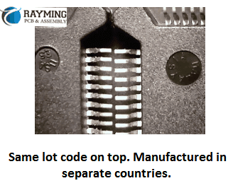
7- Verify the country of origin against the lot code number as the two lots with same code number cannot be manufactured in different countries. So for example if the country of origin name printed on suspected counterfeit part is Malaysia and other genuine part shows Philippines and both parts have same lot code number than it confirms the one is counterfeit part.
8- Examine the indents. The number one and strongest way to catch the counterfeit component is to examine the indents. Because counterfeiters have a very difficult time keeping the indents clean and consistent during their refinishing process.
For example, in the picture on the right, these two parts were received in the same lot and have identical part number markings. These are the same ends next to each other and you can see that one has 3 indents and the other has just 2. The shape and size of the indents are also different. One is a rounded cavity and the others are all flattened.
Another example of indent is this shown in the figure. The indents from the manufacturer or OCM are always clean and uniform in each and every part of the lot. However this indent shown has been filled up with blacktopping materials that was used to disguise the surface by hiding the old surface.
One more example shows the clear and obvious difference between the two parts having same part number printed from same lot. As shown in figure below the indent on one is much larger and on other it is nonexistent. This is clear and obvious example of counterfeit electronic component.
3- If not possible to buy from OCM, then go for OCM authorized dealers, suppliers or franchises
4- Look for any reputable distributor who has good reputation and customer feedback if you could not manage points 2 and 3 above
5- Deploy an inspection team that will examine the incoming parts as per the guides hints discussed
6- If you cannot deploy an inception team due to budget constraints then you can outsource the job to third party Company to avoid this headache and speed up the process.
7- Always try to avoid obsolete components in your designs but if unavoidable always look for trusted partner in component sourcing that will not deceive you.
Conclusion:
There are numerous examples of counterfeit electronic components that are floating in the electronic markets. Countless number of sellers, distributers and shops are dealing in these semiconductor electronic ICs, but it is the responsibility of the procurement division of the ECM (Electronic Contract Manufacturer) to rigorously control purchase source and always try to buy directly from OCM (Original Component Manufacturer) or any authorized dealer or franchise of OCM so that the risk of obtaining forged parts is minimized.
FPGA stands for Field Programmable Gate Array. An FPGA is an integrated circuit that can be programmed or configured by the customer or designer after manufacturing. This allows the FPGA to be customized to perform specific functions required for an application.
FPGAs contain programmable logic blocks and interconnects that can be programmed to implement custom digital circuits and systems. Unlike microprocessors that have fixed hardware function, the hardware logic and routing in an FPGA can be changed as needed by reprogramming. This makes FPGAs extremely versatile for many applications.
Some key capabilities and benefits of FPGAs include:
Customized hardware functionality
Parallel processing for high performance
Reconfigurable digital circuits
Prototyping and testing new device designs
Flexible I/O configurations
Low power consumption
Short time to market
FPGAs are widely used for prototyping of new custom ASIC designs, specialized parallel processing applications, aerospace and defense systems, automotive systems, IoT and embedded devices, and other applications requiring flexible or high-speed processing.
Major manufacturers of FPGAs include Xilinx and Intel (formerly Altera). There are many different types of FPGAs optimized for applications like high-speed processing, DSP, low power, or high I/O density.
The concept of field programmable logic devices emerged in the 1980s to fill a gap between inflexible application-specific integrated circuits (ASICs) designed for a specific task and programmable microprocessors that lacked performance for many niche needs.
In 1984, Xilinx co-founders Ross Freeman and Bernard Vonderschmitt invented the first commercially viable field-programmable gate array. This allowed circuit designers to configure the interconnections between a set of logic blocks to create custom digital circuits by programming rather than manufacturing a new chip each time.
Other FPGA companies like Actel (now Microsemi) soon followed in bringing programmable gate arrays to market. Early FPGAs were relatively simple with 1-10k gates and used in glue logic applications. As silicon manufacturing advanced, FPGA density and capabilities grew rapidly.
By the 1990s to 2000s, FPGAs with tens of thousands to over a million gates became more common. This allowed implementation of complex systems like entire microprocessors within a single FPGA chip.
FPGA architectures also evolved to add more embedded functions like memory blocks, DSP slices for math processing, programmable I/O, high-speed transceivers, and embedded microprocessor cores. Major vendors today like Xilinx and Intel produce FPGAs with billions of transistors capable of extremely sophisticated and demanding processing tasks.
FPGA Architecture Basics
The internal architecture of an FPGA consists of the following major components that can be configured:
Configurable Logic Blocks (CLBs) – The basic logic units that can implement simple Boolean functions and more complex functions. CLBs contain “look-up tables” that allow them to be programmed to perform any logic operation.
Input/Output Blocks (IOBs) – Provide the interface between the I/O pins on the FPGA chip package and the internal configurable logic. Support various signal standards.
Interconnects – The programmable routing between CLBs and IOBs. Allows flexibility in connecting internal components to implement a desired circuit function. Can include various lengths and types like global, regional, direct connects.
Memory – Many FPGAs include dedicated blocks of memory that can be used by the circuits mapped into the device. Saves integrating separate memory chips.
Embedded IP – Hard IP processor cores, DSP slices, PCIe interfaces, transceivers and other built-in functions may be included on higher performance FPGAs to optimize them for target applications.
Clock Circuitry – Managing and distributing clock signals across the FPGA is critical. Clock inputs, PLLs, DLLs, and clock buffers help achieve this.
The user programs the FPGA by specifying the Boolean logic functions for the CLBs, the interconnect wiring between blocks/IOs, use of memory and embedded IP, clocking resources, and I/O settings. This overall programming is called the configuration.
FPGA vs ASIC Differences
Xilinx Zynq fpga
FPGAs differ in important ways from Application Specific Integrated Circuits (ASICs):
FPGA
ASIC
User programmable after manufacturing
Custom manufactured for fixed function
Reconfigurable – logic can be updated
ASIC function is fixed once produced
Easier to prototype and implement changes
Costly and slow to change function once made
Parallel processing well suited for data flow applications
Often better performance and efficiency for fixed function
Generally lower volume applications
Higher volume justifies design costs
Lower development costs
Much higher development and fabrication costs
FPGAs are more flexible and quicker to develop with but less optimized in final form factor or performance than a custom ASIC. The reconfigurability and lower cost of FPGAs make them popular for low and medium volume products where custom ASICs may not be justifiable. FPGAs are also widely used to prototype ASIC designs for testing before committing to ASIC fabrication.
FPGA Design Flow
The general workflow to implement an application with an FPGA consists of the following steps:
Design Entry – The digital logic to be implemented is captured using a hardware description language like VHDL or Verilog or a schematic diagram. This is the source code describing the desired hardware functionality.
Synthesis – The source code is synthesized into lower-level Boolean logic gate representations and optimized for the target FPGA architecture.
Simulation – The design is simulated pre- and post-synthesis to verify correct functional behavior. Simulation aids debugging.
Place and Route – The logic gates are “placed” into specific FPGA hardware resource blocks and “routed” together using available interconnect paths.
Bitstream Generation – The placed and routed design is converted into a binary file that programs the FPGA configuration. This file is called the bitstream.
Configuration – The bitstream is loaded into the FPGA device to actually configure its hardware resources to implement the user’s design.
In-System Verification – The real world functionality on the FPGA is tested and debugged after configuration and integration.
FPGA vendors provide design and programming software tools to assist and automate this design flow. Popular tools include Xilinx Vivado and Intel Quartus Prime. HDL languages like VHDL and Verilog are used for design entry.
FPGA Programming Technologies
Several methods and technologies exist for programming the configurable logic in an FPGA:
SRAM Based – SRAM cells control the logic and interconnect configuration of the FPGA. Volatile, needs reconfiguring on power up. Most common approach used by major vendors.
Antifuse – One time programmable connections between logic blocks. Used in some lower cost FPGAs. Permanent once programmed.
Flash/EEPROM – Flash or EEPROM cells used for configuration cells. Allows reprogramming but nonvolatile so retains configuration on power loss.
CPLD – Complex Programmable Logic Devices have architecture between PALs and FPGAs. Smaller with more predictable timing.
Security/Encryption – Advanced FPGAs may have encryption and authentication protections on bitstreams to prevent IP theft.
SRAM programming is dominant due to its combination of reconfigurability and density. Antifuse, Flash and CPLD serve niche lower density roles. Security features help protect FPGA IP designs.
Major Applications of FPGAs
The flexibility and performance of FPGAs make them very attractive for many advanced applications including:
Aerospace and Defense – Used in guidance systems, radar processing, satellites, and mission computers where radiation-hardened FPGAs provide reconfigurable reliability.
IoT/Embedded – Provide custom logic, low power consumption, and small form factors needed for sensors, wireless, and battery-powered devices.
Image/Video Processing – Hardware acceleration for algorithms like convolutional neural networks, encoding/decoding, and analytics.
5G Telecom – High speed connectivity and processing for networking gear using FPGAs with high bandwidth I/O and DSP.
AI Acceleration – FPGA inference engines that provide optimized parallel processing for neural networks and machine learning.
Prototyping – FPGAs used to model and verify functionality of new ASIC designs before manufacture.
FPGAs continue growing in capability and bridging into applications traditionally addressed by CPUs and GPUs. Their flexibility makes them the ideal choice when custom hardware acceleration is needed.
The FPGA market continues to see intense innovation and new entrants even as it consolidates around Xilinx and Intel. The growth of 5G, AI, embedded vision, and other applications is driving demand for more advanced programmable logic solutions.
Trends and Innovations in FPGAs
FPGAs continue to evolve rapidly to increase capabilities and provide advantages over other processing technologies for specialized requirements:
Heterogeneous Integration – Combing FPGA fabric with hard processor cores (ARM, RISC-V), transceivers, memory, analog, etc. on a single chip provides “system-on-chip” capability.
High Level Design – Raising design abstraction above HDLs by using C/C++, OpenCL, MATLAB, and other languages to describe FPGA behavior. This expands accessibility.
3D Packaging – Stacking FPGA dies and integrating with other dies like HBM memory enables much higher bandwidth and density.
Security – Root of trust, bitstream encryption/authentication, and other features to protect FPGA configuration and IPs from tampering or theft.
Cloud/Datacenter – Adoption in public cloud FaaS offerings and datacenter acceleration using FPGAs for their flexibility and performance per watt.
Soft MCUs – Soft microcontroller cores implemented internally within an FPGA for low cost embedded applications.
AI Acceleration – Optimized FPGA deep learning processors for inference using low precision and quantization to achieve efficiency.
FPGAs will continue to blur into adaptive computing devices as they evolve beyond basic programmable logic into heterogenous systems-on-chip. Their flexibility to reconfigure hardware logic on the fly makes them a foundational technology for the future.
Frequently Asked Questions
What are the main differences between FPGAs and CPLDs?
Complex Programmable Logic Devices (CPLDs) differ from FPGAs in several ways:
Less logic capacity – typically thousands not millions of gates
Based on sum-of-products architecture
Optimized for predictable timing
Live at power up (no configuration bitstream)
Often lower cost and power
Can be built-in flash/OTP instead of SRAM
So CPLDs serve simpler glue logic roles rather than implementing complex systems like FPGAs.
What are the advantages of using VHDL vs Verilog for FPGA design?
VHDL tends to be preferred for larger ASIC and FPGA designs requiring rigorous verification for manufacturability. Verilog started as a simulation language and is popular with front-end designers. Key differences:
VHDL
Strongly typed, English-like syntax
Large set of data types
Excellent tool support
Suited for verification & top-down modeling
Verilog
C-like syntax, weaker typing
Fewer data types
Suited for behavior modeling
Fast simulation, prototyping
Widely used in education
How are FPGAs programmed/configured?
Most FPGAs are SRAM-based and programmed by loading a bitstream:
Design logic is created and outputs a binary bitstream file after place & route
On power up, bitstream loads from flash/storage into SRAM cells
SRAM settings define logic, I/O config, routing to implement design
This can be reprogrammed by flashing a new bitstream
So FPGAs provide complete hardware configurability via programmable SRAM-based bitstreams.
What types of CAD tools are used for FPGA design?
Common FPGA CAD tools include:
Xilinx Vivado – For synthesis, place & route, bitstream gen
FPGA vendors like Xilinx provide integrated environments that take design entry through bitstream. Additional tools help with simulation, PCB design, IP reuse, and C-level design.
What are the main challenges when working with FPGAs?
Some common challenges with FPGA design include:
Steep learning curve programming with HDLs like Verilog and VHDL
Complex toolchains require expertise to optimize through the flow
Timing closure and routing congestion as designs push capacity limits
Power usage control and thermal management
Debugging within hardware description languages
Cost of tools and IP add to development overheads
Staying current as architectures rapidly evolve
But continuous improvements in design tools, abstraction levels, and embedded debug capabilities are helping overcome these challenges.
Summary
FPGAs are integrated circuits whose logic and routing can be reconfigured after manufacturing. This provides hardware-level flexibility compared to fixed-function ASICs. FPGAs contain logic blocks, I/Os, and interconnects that can be programmed using HDL or schematic design entry.
Leading FPGA applications include aerospace/defense systems, 5G infrastructure, automotive electronics, IoT devices, and hardware acceleration for AI inferencing. Major vendors are Xilinx and Intel/Altera, but new entrants continue to push innovation in FPGAs for embedded, cloud computing, networking, and other uses.
Trends in FPGA evolution include heterogenous integration, raised abstraction levels, 3D packaging, and security. As FPGAs grow beyond basic programmable logic into adaptive computing platforms, they will play an increasingly important role in diverse electronic systems.
An Introduction to FPGA
FPGA stands for (Field Programmable Gate Array). As the name implies, the FPGA is an integrated circuit (IC) that is basically an array of logic gates and is programmed/configured by the end user in the field (wherever he is) as opposed to the designers.
The basic logic gates are the core building blocks of the FPGA. It is not like the FPGA IC is full of these logic gates, but FPGA is based on digital sub-circuits carefully interconnected with each other to perform the desired function. It is like for example to make a shift register the AND gates and OR gates ICs are required, so there are two ways either to buy these individual ICs and interconnect them together to obtain the functionality of Shift register. The other way is to buy a shift register IC instead and make your design much more compact.
This is the case with FPGA assembly, the sub-circuits are already made of basic AND, OR and NOT gates and these sub-circuits are then interconnected very accurately to design the internal hardware blocks called Configurable Logic Block (CLB).The CLBs can also be defined as Look up Tables (LUT) that is programmed by Hardware Description Language (HDL) to achieve desired output.
These thousands of CLBs are then connected with IOBs to interface with external world circuitry. The IOB stands for “Input Output Blocks”. These IOBs are made of pull up, pull down resistors, buffer circuitry and inverter circuits.
Reprogram-ability of FPGA:
The biggest advantage of FGPA is its ability to be reprogrammed at the field. Its flexibility to be used as microprocessor, graphic card or image processor or all of them at the same time make it solid upper hand to basic micro-controllers or micro-processors.
These FPGAs are programed by HDL like VHDL or Verilog. Some additional features are being added nowadays in FPGAs like dedicated hard-silicon blocks for attaining functions of External Memory Controllers, RAM block, PLL, ADC and DSP block and many other components.
Difference between the Micro-controller and FPGA:
Today, many of the projects are based on micro-controllers. As our trend in developing student project, professional circuits, industrial products development is based on micro-controller based circuits, we did not got much familiarized with FPGAs.
The main difference between the micro-controller and FPGA is that, “A micro-controller is versatile IC and can be programmed in different ways to fit in various types of applications while the FPGA is a dedicated IC specifically designed to perform special functions according to the needs of a particular application”.
Another important difference is that “The FPGAs are hardware Configurable Logic Blocks (CLBs) based ICs that can be interconnected to external circuits through Hardware Description Language HDL codeby means of IOBs while micro-controllers are based on software/programming/coding where instructions are executed sequentially.”
The micro-controller / micro-processor has constraints of inability to execute multiple instructions simultaneously and also functionality you want to perform must have the availability in instructions sets of a particular controller/processor.
The FPGAs are somewhat similar to ASIC “Application Specific Integrated Circuits” but not very much. The key difference in FPGA and ASIC is that CLBs in FPGA can be reconfigured to perform different task/operation/function but in the case of ASIC the dedicated ASIC chip will perform the same operation for the entire life time for which it was designed.
The analogy of FPGA and ASIC is that you build a house using LEGO parts, then you demolish it and built a car using same LEGO parts. These LEGO parts are same as CLBs of FPGA.
The analogy of ASIC is that you build the same house using concrete blocks and cement (not the LEGO) but now you cannot demolish it and build other thing from this. This work is permanent. Hence this is ASIC.
So the ASICs are dedicated ICs in which digital circuitry (logic gates and sequential circuits) is hardwired or permanently connected internally on silicon wafer.
FPGAs are suitable for low volume production and require much less time and money as compared toothier ASIC counterparts. FPGAs require less than a minute to reconfigure. Another important advantage is that FPGAs can be partially reconfigured and rest of FPGA portion is still working.
However, FPGAs on the other hand are slower and more power hungry due to their large area size due to dense routing programmable interconnection. This complex interconnection accounts for 90% of the total size of FPGA.
Detailed Insight of FPGA Structure:
The main constituents of FPGA are
Configurable Logic Blocks (CLBs)
Input Output Blocks (IOBs)
Switch Box (SB)
Connection Box (CB)
Look Up Table (LUT)
Horizontal and Vertical Routes
Configurable Logic Block (CLB):
A CLB is made up of the cluster of BLE (Basic Logic Element) through a dense interconnect scheme. A BLE has the multiplexer, SRAM and D Type Flip Flop. These three components forms the BLE and the cluster of BLEs form the CLB
Input Output Blocks (IOBs):
These are the blocks that make interconnection between the FPGA and outside circuitry. The IOBs are the end connection of the programmable routing network.
Switch Box (SB):
Switch Box is the collection of switches to connect different horizontal and vertical routes (tracks). Ability of a track to connect to multiple tracks is defined as the connectivity of SB.
Connection Box is the collection of switches to connect CLB to multiple routes. Ability of the CLB to connect to multiple routes/tracks is defined as the connectivity of CB
Look Up Table (LUT):
The lookup table is made of multiplexer and SRAM. A 4 input LUT requires (24) 16 SRAM bits to implement a 4 bit Boolean expression.
Horizontal and Vertical Routing Channels:
The horizontal and vertical lines/routes that creates the mesh network of FPGA
Flexibility of CB:
The flexibility of CB is defined as (FC). A FC = 1 means that all the adjacent routing channels are connected to the inputs of CLB
Flexibility of SB:
The flexibility of SB is defined as (FS). It is defined as the total number of tracks with which every track entering the SB connects to.
Conclusion:
It is therefore concluded that FPGAs have advantages over other options like ASIC and microprocessor / micro-controller in the sense that FPGAs are handy and easily reconfigurable at the user end. It can be customized by a simple HDL code and are easily available in the market for reasonable rates between 50 to 100 USD.
A programmable logic controller (PLC) is a digital computer used for automation of industrial processes, such as control of machinery on factory assembly lines. PLCs can be programmed to perform logical functions, timing, counting, arithmetic, and data handling tasks needed for controlling industrial equipment and processes.
PLCs have input and output devices that allow them to monitor and control machines and processes. The input devices collect data from sensors that measure things like temperature, pressure, speed, etc. The PLC then processes this data according to a program and determines what the output devices connected to it should do in response. The output devices can control actuators, valves, motors, lights, or other equipment.
History of PLCs
The origins of PLCs go back to the late 1960s when the automotive industry was seeking a way to replace complex relay-based control systems with a more flexible, software-driven approach. Engineers at General Motors (GM) developed the first PLC, introduced in 1968 under the trademarked name Programmable Logic Controller.
GM’s early PLCs used ladder logic diagrams, borrowing from the relay-based control systems they were replacing. Ladder logic made PLC programming more intuitive for engineers accustomed to working with electrical control schematics. The first PLCs had limited memory and logic compared to modern devices, but already offered major advantages in terms of flexibility, ease of programming, and reliability.
PLCs were soon adopted by other industries like steel mills, chemical plants, and food processing due to their ability to control complex systems safely and efficiently. As technology advanced, PLCs became more sophisticated and powerful. Early PLCs could only handle boolean (on/off) logic but later versions introduced more complex functions like timers, counters, arithmetic, and analog I/O handling.
Today’s PLCs are highly advanced computation and control devices capable of managing entire automated factories and processes with precision and reliability. Major PLC manufacturers include Allen-Bradley, Siemens, Mitsubishi, Omron, and Schneider Electric.
PLCs provide many benefits that make them invaluable for industrial automation and process control:
Flexibility – PLC logic can be reprogrammed when needed to make changes or implement improvements in the controlled system. This avoids having to rewire circuits or rebuild equipment when system changes are needed.
Reliability – PLCs are solid state devices with no moving parts that can operate for years in harsh industrial environments like dust, moisture, vibration, and extreme temperatures. This makes them highly reliable compared to electromechanical relays.
Scalability – Most PLCs can be expanded and reconfigured to add I/O points and capabilities. This allows the control system to grow over time as new sensors, processes, or equipment are added.
Ease of Programming – Ladder logic and other PLC programming languages are relatively easy to learn. Programs can be simulated on a PC before loading into the PLC. Troubleshooting and editing programs is straightforward.
Communication Capabilities – PLCs can communicate with other devices and controllers on local networks and larger distributed control systems. This allows coordination and monitoring across an entire automated facility.
Cost Effectiveness – Although the initial investment is higher than simple relays, PLCs offer very competitive long-term value given their flexibility, expandability, and durability.
Enhanced Control Capabilities – PLCs can implement advanced regulatory control, motion control, data acquisition, alarm handling, and other sophisticated automation functions beyond simple on/off control.
How PLCs Work
The basic operation of a PLC involves three primary functions:
Input Scan – The PLC gathers input data from connected devices like sensors, switches, push buttons, etc. It examines the status of these input devices and saves their on/off states to memory.
Program Scan – The PLC then executes the logic program, line-by-line, examining the input states and running any logic instructions programmed by the user. During this scan, the PLC may energize and de-energize internal relay coils based on programmed logic. The results or “solutions” are stored in memory.
Output Scan – Finally, the PLC updates the physical output devices like motors, lights, valves, etc. based on the internal memory solutions from running the user program. The updated outputs then cause a change in the controlled process or machine.
These input-processing-output scans repeat many times per second to achieve real-time automation control. The PLC program determines exactly how the PLC will react to various inputs with appropriate outputs.
PLC Hardware Components
The main hardware components of a PLC include:
Processor – This is the central processing unit or “brain” containing the main memory, arithmetic logic unit (ALU), control unit, and instruction set to execute the PLC program.
Power Supply – Provides regulated DC power to the PLC processor, I/O modules, and field devices. Usually 24VDC.
I/O Modules – Interface between field devices and the PLC processor. Analog I/O modules convert sensor measurements to digital data. Discrete I/O modules convert device states to on/off signals the PLC understands.
Communication Modules – Allow the PLC to communicate with HMIs, data networks, remote I/O racks, and other devices. Common methods are Ethernet, serial, WiFi, and fieldbus modules like Profibus and Modbus.
Chassis or Backplane – Metal enclosure housing the processor, power supply, and I/O modules and providing internal communication buses.
Programming Device – Portable unit used to program the PLC. Can be a laptop, programming panel, or proprietary programmer. Connects to the PLC via USB, Ethernet, or other methods.
PLC Programming
PLCs are programmed using special software running on a PC or laptop. Programming involves three main steps:
Design the program logic and enter via programming software.
Simulate and debug program offline on the computer.
Download tested program to the PLC for execution.
There are different techniques and languages used for PLC programming:
Ladder Logic
The most common PLC programming method which uses ladder diagrams based on circuit diagrams. Ladder logic has contacts, coils, instructions, and functions.
Example Ladder Rungs
Structured Text
Similar to Pascal programming language using statements, functions, variables, and other high level code structures.
Example Structured Text
Copy code
IF Level > 10 THEN Valve = Open ELSE Valve = Closed END_IF
Function Block Diagrams
Graphical language representing logic as interconnected function blocks. Used in continuous control systems.
Example Function Block
Instruction Lists
Low level basic instructions similar to assembly code. Not as commonly used today.
Ladder logic is the most popular and widespread PLC programming language because it is easy to learn and mirrors old relay control schematics. But other languages are gaining use for more advanced functions.
Choosing a PLC
Factors to consider when selecting a PLC:
Number and type of I/O required (analog, digital, specialty modules)
It is best to select a PLC model that offers built-in room for expansion in case your I/O or program memory needs grow in the future. Getting the right PLC for an application involves balancing performance, capabilities, and cost.
Modern PLCs communicate with many other devices and systems using a variety of networking methods and protocols. Communication capabilities a PLC may have include:
Programming – Used to upload/download programs from a PC to the PLC. Connections such as USB, Ethernet, RS-232, RS-485.
HMIs – Human-Machine Interfaces like industrial PCs and touch screens connected to a PLC to display system data and allow operators to monitor and control the process.
SCADA Systems – Supervisory Control and Data Acquisition systems connected to multiple PLCs and HMIs to monitor and control an entire factory or facility from a central computer.
Industrial Networks – PLC communication with other PLCs on high speed networks like Ethernet/IP, Modbus TCP, and EtherCAT to coordinate distributed control systems.
Fieldbuses – Connecting PLCs to remote I/O devices, drives, sensors using fieldbus networks like Profibus, Modbus RTU, and DeviceNet.
Wireless – Technologies like WiFi and cellular allowing PLCs to communicate wirelessly with mobile HMIs, data historians, asset management systems, and remote troubleshooting devices.
PLC Applications
PLCs are highly versatile devices used for automation in many industries and applications including:
The flexibility, computing power, and communication capabilities of modern PLCs make them a fundamental component of automated systems in virtually all industrial sectors.
Advantages and Disadvantages of PLCs
Advantages:
Flexible, customizable programming
Reliable and rugged industrial computing platform
Built-in communications for networking and HMI connectivity
Scalable I/O configurations
Advanced capabilities beyond basic control (motion, data collection, etc)
Integrated diagnostics and troubleshooting
Mature technology with deep application knowledge base
Disadvantages:
Higher initial investment cost than simpler controls
Requires electrical design and programming skills
Advanced functions may require costly specialized modules
Troubleshooting problems requires specialized tools and training
Proprietary programming languages vary by manufacturer
The Future of Programmable Logic Controllers
PLCs will continue advancing in response to the needs for more sophisticated automation and “smart manufacturing” concepts. Key developments shaping the future of PLC technologies include:
Hardware advances – Smaller, more powerful, faster, cheaper PLCs with denser I/O and specialized modules
Increasing emphasis on software, connectivity, and remote access rather than just hardware logic
Use of PC-based controllers and soft PLCs running on industrial PCs
Programming enhancements integrating IEC 61131-3 languages with object-oriented extensions
Pressure Sensors – Measure liquid, gas, or hydraulic pressures.
Flow Sensors – Measure liquid or gas flow rates.
Level Sensors – Measure liquid levels in tanks or vessels.
What are the main advantages of PLCs over relay logic?
PLCs offer numerous advantages compared to traditional relay circuits:
Flexible programming that is easier to change
Much faster response and scan times
Not susceptible to contact issues like sticking or corrosion
Higher density I/O in smaller space
Communication and data collection abilities
Advanced capabilities beyond basic logic
How do you troubleshoot problems with a PLC?
Common techniques for troubleshooting PLC issues include:
Monitoring status LED indicators on modules
Checking I/O signals with a handheld digital tester
Verifying proper voltage at power supply and I/O modules
Uploading program to computer to check logic and spot errors
Monitoring PLC diagnostics memory addresses
Forcing inputs/outputs manually or inserting simulator signals
Checking communication connectivity and data flow
Comparing behavior to simulation programs or known good backups
What precautions are important when wiring inputs and outputs to a PLC?
Key wiring precautions include:
Separating AC power wires from DC I/O wiring
Properly grounding the PLC and field devices
Using shielded, twisted pair cables for analog signals
Avoiding running I/O wiring in parallel with power cords
Keeping wire lengths short to avoid electrical noise issues
Double checking wiring before energizing
Verifying rated voltage and current limits
Following all electrical safety procedures
How can better cybersecurity be ensured for PLC systems?
PLCs used for critical infrastructure need protections like:
Blocking unused communication ports
Disabling unnecessary services and protocols
Encrypting network traffic where possible
Using whitelisting to only allow authorized access
Proper password policies and access controls
Virtual private networks (VPNs) for remote access
Security tools like firewalls, intrusion detection, backups
Physical security restricting physical PLC access
Regular penetration testing to find vulnerabilities
Summary
Programmable logic controllers or PLCs are rugged, reliable computerized control systems used for automation in industrial applications. PLCs contain a processor, power supply, I/O modules, and communication modules housed in a chassis. Input devices like sensors are monitored by a PLC which then runs a logic program to determine the appropriate response from output actuators according to programmed instructions.
Ladder logic is the most common PLC programming language, but other methods like structured text and function block are also used. Leading PLC brands include Allen-Bradley, Siemens, Omron, and Mitsubishi. Choice of PLC depends on factors like number of I/O, speed, memory, and communications requirements.
PLCs provide flexible, scalable, and reliable control well-suited for harsh industrial environments. They offer advanced capabilities beyond what could be achieved with simple relays. Modern PLCs incorporate sophisticated communications, HMIs, motion control, safety systems, data collection, and more. PLCs will continue advancing in response to automation needs for IoT connectivity, machine learning, and other smart technologies.
Micro-electromechanical systems, or MEMS, are tiny integrated devices that combine mechanical and electrical components on a common silicon substrate. MEMS extend the fabrication techniques developed for the integrated circuit industry to add mechanical elements like beams, gears, diaphragms, and springs to chips.
In this comprehensive guide, we will cover:
The components and operating principles of MEMS devices
Various types of MEMS sensors, actuators, and other applications
MEMS materials, manufacturing processes, and packaging
Design and simulation considerations for MEMS
Current and future applications using MEMS
MEMS industry landscape and key players
Advantages and challenges with MEMS technology
FAQs
By the end, you’ll have a solid grasp of what micro-electromechanical systems are, how they work, where they are used, and their impact. Let’s get started!
Micro-electromechanical systems integrate miniature:
Sensors – To detect physical phenomena like motion, pressure, chemical levels, etc. Common examples include accelerometers, gyroscopes, pressure sensors, and gas sensors.
Actuators – To provide physical movement or action. Examples include micromirror arrays, valves, pumps, and manipulators.
Electronics – To process signals from sensors and control actuators. The circuitry includes components like ASICs, capacitors, transistors, and bond pads.
Mechanical Structures – The micromachined components that enable physical functionality like cantilevers, gears, membranes, channels, and diaphragms.
By combining these miniaturized elements on a chip, MEMS enable new categories of tiny sensors, actuated devices, and integrated systems not achievable with conventional electronics.
MEMS operate through principles like:
Thermal actuation
Piezoelectric transduction
Capacitive sensing
Electrostatic actuation
Resonant energy harvesting
Microfluidic control
These enable functions difficult to implement conventionally at such small scales. Cutting edge fabrication techniques make MEMS possible.
Types of MEMS Devices
There are several major categories of MEMS devices:
MEMS Sensors
Sensors detect physical phenomena and convert them into electronic signals for processing.
Accelerometers – For measuring acceleration and tilt along 1, 2 or 3 axes. Critical for airbags, phones, navigation, vibrations, and more.
Gyroscopes – Measure angular velocity and orientation in space. Used in drones, VR/AR, robotics, and other applications needing precision orientation.
Pressure Sensors – Gauge applied pressure. Used in weather monitoring, touchscreens, biomedical devices, and more.
Chemical Sensors – Detect gaseous chemicals and concentrations. Enable smart gas detection and analysis.
Inertial Measurement Units – Combine accelerometers and gyroscopes to precisely track motion and orientation for navigation and guidance.
Resonant Sensors – Vibrating MEMS structures shift frequency based on mass or other changes, allowing extremely precise measurements.
MEMS Actuators
Actuators provide movement or mechanical action. Examples include:
Micromirror Arrays – Control light beams by tilting tiny mirrors for displays, scanning, and fiber optics.
Microvalves – Regulate fluid flows in miniature channels and pipes. Used in miniature gas chromatography systems, lab-on-a-chip devices, etc.
Optical Switching – Route optical signals between fiber optic channels. Used in telecommunications and data networking equipment.
RF MEMS Switches – Switch high frequency electrical signals for tuned impedance matching and signal routing. Used in tunable filters, phased arrays, and reconfigurable antennas.
Microspeakers – Vibrate to generate sound waves and audio output. Used in earphones and integrated device sound.
MEMS Pumps – Generate controlled microfluidic flows or pressure differentials. Used for drug delivery, analyte sampling, microcooling systems, etc.
Other Types of MEMS
Beyond sensors and actuators, other types of MEMS include:
Microfuel cells – Generate electricity from fuel sources through electrochemical reactions on a chip.
Micromotors – Spin tiny rotors using electromagnetic forces or thermal actuation. Used for micro gears, pumps, and other mechanisms.
Microbolometers – Measure infrared radiation for thermal imaging applications. Used in fire detection, autonomous vehicles, and security cameras.
Microneedle patches – Contain arrays of microneedles for drug delivery through the skin.
The diversity of MEMS devices enables sophisticated miniature systems across a huge range of applications, as we’ll explore next.
Silicon is the most common substrate material due to well-controlled microfabrication techniques developed by the IC industry.
Other options include glass, ceramics, metals, and polymers.
Deposition Processes
Depositing thin films of structural and sacrificial materials through processes like chemical vapor deposition (CVD), sputtering, and molecular beam epitaxy.
Lithography
Patterning masks and exposing photoresists using techniques like photolithography, e-beam lithography, and X-ray lithography.
Etching
Removing material selectively through wet etching with acid solutions or dry etching using plasma.
Doping
Ion implantation and diffusion to dope structural layers like polysilicon with boron, phosphorus or other dopants.
Bonding
Anodic bonding of micromachined silicon wafers with glass layers.
Micromachining
Bulk micromachining to selectively etch inside silicon or other substrates.
Surface micromachining to build structures by patterning layers on top of the substrate.
Careful sequencing of these microfabrication steps allows constructing the mechanical and electrical components needed for MEMS.
MEMS Packaging
Once fabricated, MEMS dies require specialized packaging to:
Protect delicate MEMS structures from damage
Facilitate required gas or fluid flows
Allow space for movements
Electrically connect bond pads
Mount components like application-specific integrated circuits (ASICs)
Enable integration into larger systems
Common packaging approaches include:
Ceramic and plastic packaging
Wafer-level packaging and encapsulation
Multi-chip module packaging
Printed circuit board integration
Innovations in MEMS packaging continue advancing capabilities while reducing size and cost.
MEMS Design and Simulation
Designing MEMS requires cross-functional physics simulation and modeling tools. Key analyses performed include:
Mechanical – Stress, vibration, fatigue life, resilience, etc.
Electrical – Drive circuitry, feedback signals, noise, etc.
Fluidic – Air/liquid flows, pressure differentials, turbulence, etc.
Optical – Light reflection, diffraction, scattering, etc.
Each MEMS application has unique multiphysics requirements that must be modeled across mechanical, electrical, fluidic, and thermal domains synergetically.
Standard 3D CAD tools combined with multiphysics solvers address MEMS modeling needs for precision design optimization.
Current and Future Applications of MEMS Technology
Thanks to their tiny size, low cost, and sophisticated functionality, MEMS devices are enabling innovative applications across every industry:
Transportation – Inertial guidance, ESP, safety sensors in airbags, tire pressure monitoring, etc.
Consumer Electronics – Accelerometers, gyroscopes, microphones, and displays in smartphones, game consoles, etc.
Medical – MEMS pressure sensors in catheters, microneedle drug delivery, implants, diagnostics.
Industrial – MEMS accelerometers for vibration monitoring, gas sensors for leak detection, microvalves for control.
Defense – MEMS inertial measurement units in missiles and drones, chemical threat detection, research into MEMS robots and smart dust.
Auto – Tire pressure sensors, inertial sensors, infrared detectors for night vision systems.
The next wave of innovation in self-driving vehicles, IoT devices, AR/VR, Industry 4.0, and more will be enabled by MEMS. The opportunities are boundless thanks to the unique capabilities MEMS provide.
MEMS Industry Landscape
MEMS
The global MEMS industry is projected to grow to around $90 billion by 2025. Key players include:
Semiconductor foundries like TSMC, GlobalFoundries, and SMIC that fabricate MEMS devices.
Fabless MEMS designers including STMicroelectronics, Bosch Sensortec, InvenSense, and mCube.
IDMs with internal MEMS manufacturing like Texas Instruments and Analog Devices.
Applied Materials, SUSS MicroTec, and DISCO providing fabrication equipment.
OSATs packaging and testing MEMS including ASE, Amkor, and JCET.
Automotive Tier 1s producing MEMS sensors for vehicles, such as Denso, Delphi, and Infineon.
While initially driven by a small group of IDMs, today’s MEMS industry involves an advanced supply chain enabling high volume foundry production. Economies of scale continue driving increased adoption.
Advantages and Challenges of MEMS
Some key benefits MEMS provide versus conventional implementations:
Benefits
Extreme miniaturization impossible through other means
Fully integrated devices combining electronics and mechanical elements
Low power consumption due to reduced size
Cost effective high-volume fabrication
Performance improvements from scaling effects
Challenges
High development costs and long design cycles
Need for advanced modeling and simulation skills
Strict process controls and expertise required
Packaging for protection while allowing operation
Metrology of 3D microscopic features
By capitalizing on their advantages while navigating inherent challenges, MEMS stand to revolutionize nearly every industry much like ICs did for electronics.
Frequently Asked Questions
Here are some common MEMS-related questions:
Q: How small are MEMS devices typically?
A: MEMS range from 20 micrometers to 1 millimeter. Very small yet large enough to allow practical microfabrication. State-of-art processes steadily allow smaller MEMS over time.
Q: How are MEMS different from ICs?
A: While fabricated similarly to ICs, MEMS add physical micromechanical structures rather than just electronic circuits. This allows mechanical sensing and actuation.
Q: Are MEMS always made from silicon?
A: Most use silicon substrates due to readily available silicon micromachining techniques from the IC industry. But some MEMS leverage materials like polymers.
Q: How durable and reliable are MEMS components?
A: MEMS can last decades in many applications with careful design. However, certain environments with high temperatures, pressures, radiation or contaminants can impact reliability.
Q: Are MEMS expensive to produce?
A: MEMS fabrication has high upfront costs for masks and process development. However, the per unit costs become very affordable in high volume thanks to batch manufacturing principles.
Conclusion
In summary, micro-electromechanical systems fuse electrical and mechanical components on integrated chips to enable transformative applications. With ongoing innovations in manufacturing and design, MEMS will continue growing as a key technology across industries from automotive to medical to consumer electronics and more. Their unique advantages of microscopic size, integration, low cost, and sophisticated performance open up new possibilities. While engineering MEMS requires specialized expertise, the benefits make the investment well worth it for next-generation products and capabilities.
Resistors are one of the most fundamental components used in electronics and electrical circuits. To easily identify resistor values, a color coding system is commonly used to mark the resistance on the body of the resistor.
Learning how to read these color codes is an essential skill for anyone working with electronics. In this comprehensive guide, we will cover:
What resistance and resistors are
Resistor color code systems
3 band
4 band
5 band
Decoding color bands to read resistance value
Calculating resistance from color codes
Determining tolerance from color code
Identifying special values like EIA
Practical examples and exercises
Common mistakes to avoid
Other resistor markings
Frequently asked questions
After reading this tutorial, you will be able to easily decipher the color codes to determine the resistance value of any common resistor. Let’s jump in!
To understand resistor color codes, we first need to understand what resistance means and what resistors are.
Resistance is the property of a material that opposes the flow of electric current. It is measured in ohms and represented by the Greek symbol Ω.
Resistors are electrical components explicitly designed to provide resistance in a circuit. Some key properties of resistors:
Made of resistive materials like carbon, wire windings, metal oxides
Designed with a certain resistance value
Used to limit current flow, divide voltages, damp signals, and more
Available in many form factors like axial, SMD chip, rectangular, etc.
By adding resistors into circuits, we can finely control voltages and currents as needed. But to utilize them properly, we need to know their resistance values. This is where resistor color coding comes in.
Resistor Color Code Systems
There are a few standards for marking resistance values on resistors with colored bands. Let’s look at the common systems.
3 Band Color Code
This system uses three colored bands to denote the resistance as follows:<img src=”https://imgur.com/BEnfSfR.png” width=”200″>
1st and 2nd band – Digits for resistance value
3rd band – Multiplier
(Optional 4th band – Tolerance)
For example, green-blue-red equates to a 56 x 100 = 5600 Ω resistor. Very simple and common coding.
4 Band Color Code
This expands the 3 band code by adding a 4th tolerance band:<img src=”https://imgur.com/gBrjaXR.png” width=”200″>
1st band – 1st digit
2nd band – 2nd digit
3rd band – Decimal multiplier
4th band – Tolerance
So yellow-violet-red-gold decodes to 47 x 100 = 4700 Ω with 5% tolerance.
5 Band Color Code
This further expands the code with an extra significant figure digit:<img src=”https://imgur.com/Tbye4Wf.png” width=”250″>
1st and 2nd band – 1st and 2nd digit
3rd band – 3rd digit
4th band – Multiplier
5th band – Tolerance
For example, brown-black-orange-red-gold equates to 10,000 x 100 = 1,000,000 Ω ± 5% tolerance.
This allows expressing higher resistances with greater precision.
The color of the tolerance band indicates the precision of the marked resistance value. Common tolerances include:
Brown – ±1%
Red – ±2%
Gold – ±5%
Silver – ±10%
None – ±20%
Higher precision resistors have tighter tolerances printed on them. For example, a gold band means the actual resistance should be within ±5% of the marked value.
So a 100 Ω ± 5% resistor can have an actual resistance between 95 to 105 Ω. Tolerance gives the acceptable margin of error.
Identifying EIA Values
There is also a special variant of 4-band color codes for EIA preferred values. It is denoted by:
1st and 2nd bands – Standard codes
3rd band – Decimal multiplier
4th band – Gold or silver ±5% tolerance
Gold as 4th band = EIA value x 0.1 Silver as 4th band = EIA value x 0.01
For example:<img src=”https://imgur.com/N5MWUqf.png” width=”200″>
Red-Red-Gold = 22 x 0.1 = 2.2 Ω
Brown-Black-Silver = 10 x 0.01 = 0.1 Ω
Both are standard EIA values. This code helps identify them.
Practice Exercises
Let’s practice decoding some example resistor color codes:
Orange-Orange-Red
Brown-Green-Brown-Silver
Red-Violet-Yellow-Gold
Blue-Grey-Black-Brown
Green-Brown-Orange-None
Scroll down to check your work!
Solutions:
33 x 100 = 3300 Ω
15 x 10 = 150 Ω ± 10% tolerance
27 x 10,000 = 270,000 Ω ± 5% tolerance
68 x 1 = 68 Ω ± 1% tolerance
58 x 1000 = 58,000 Ω ± 20% tolerance
How did you do? With practice, you will be able to read resistor codes effortlessly.
Common Mistakes
Here are some common mistakes to avoid when decoding resistor color codes:
Forgetting the multiplier – Make sure to apply the multiplier band or else your value will be way off.
Mixing up tolerance and multiplier – It’s easy to flip these two adjacent bands by accident. Double check their order.
Misreading similar colors – Red/orange or blue/violet can look alike on small resistors. Take care!
Assuming wrong # of bands – Always confirm the band count before reading the resistor.
Decoding non-standard codes – Some resistors use custom codes. Verify it is a standard scheme.
Faded colors – If bands fade to almost white, they may be indistinguishable.
With experience, you will learn to avoid these pitfalls. When in doubt, check the datasheet or use a multimeter to measure the actual resistance.
Other Resistor Markings
While color coding is the most common, resistors may also be marked in other ways:
Multiplier written numerically such as 10M or 10MΩ for 10 million ohms
Tolerance written out like ±5% rather than color band
3 or 4 digit codes starting with the multiplier e.g. 471 = 470Ω
Actual resistance printed numerically e.g. 10k
SMD resistors marked with just a number string
So you may encounter alternate formats beyond the standard color codes. With practice, you’ll learn to interpret all the common schemes.
Frequently Asked Questions
Here are some common questions about resistor color codes:
Q: Why are colors used instead of just printing the resistance value?
A: The color bands allow cheap, permanent, and unambiguous marking without requiring printed text or symbols.
Q: What do more than 3 bands indicate on a resistor?
A: Additional bands denote tolerance and extra significant figure digits for higher precision.
Q: Why do resistors have a tolerance?
A: Due to manufacturing variations, the actual resistance cannot match the target value exactly. Tolerance specifies the allowable error range.
Q: What is the gold or silver multiplier on 4-band resistors?
A: These denote EIA preferred values. Gold = multiply by 0.1, silver by 0.01.
Q: Can you read a resistor’s value without decoding the color bands?
A: Yes, you can directly measure a resistor’s resistance using a multimeter if you need to confirm its value.
Conclusion
Understanding resistor color coding is indispensable for working with resistors in circuit design and analysis. This guide provided a comprehensive overview of decoding color bands including:
Resistor coding systems – 3, 4, and 5 band
Looking up digit values, multipliers, and tolerance
Calculating resistance from color codes
Identifying EIA values
Avoiding common mistakes
Handling non-standard markings
With this knowledge, you can now easily decipher resistor color codes and determine resistance values. Receiving a handful of resistors is no longer an intimidating puzzle!
Practice reading a variety of example resistor color codes until it becomes second nature. Mastery of these fundamentals will give you confidence working with resistors and building circuits.
BGAis the abbreviation of Ball Grid Array. This, in a general form, is an array of small sized / tiny metallic conductor balls that are arranged in a harmonies form on the Board that we proceed towards making a PCB. Nowadays; due to increased demand of only BGAs, companies (manufacturers) has formed (Example- Xilinx).
These balls are eventually used to making connections using small and precise soldering while putting microprocessors and integrated circuits; in order to make the complete circuit that we intend to make / work out for. The process of connecting the small balls is called SMT (Surface Mount Technology).
Reason of BGA being so popular in modern technology:
There is a bunch of reasons why modern technology depends on BGA on a great extent. The most important one is that, BGA has superlative thermal dissipation capability, making the core to be cool while in operation; hence prolonging the products lifetime. Heat is the most important measure to deal with and BGA is the reason why tech products work so smooth while being normal in temperature while working at even full load. Second most important reason is the electrical properties. The shortest distance connections with lower possible resistive ways make the purpose of using BGAs even more valuable and worthy. Third most important reason is Compatibility. Being able to use the smallest space while working with greater number of balls allows the manufacturer to place more and more workable options in the product that makes it even more valuable and of value. This is indirectly related to lower production cost while making valuable and better priced products for the production and market customers.
Types of BGA:
There are different types of BGA that are being used in most of the countries by most of the manufacturers but the most popular ones and widely used ones are detailed below with a short description to each-
PBGA (Plastic Ball Grid Array):
PBGA is the abbreviation of Plastic Ball Grid Array. This is the most popular type for double-sided PCBs that are being used recently. It was first invented by the company MOTOROLA and is now being used widely by most of the manufacturers. The core is of bismaleimide triazine (BT) resin that is used as the substrate material. This along with the application of over molded pad array carrier (OMPAC) sealant tech or glob to pad array carrier (GTPAC) is highly reliable and is verified by JEDEC (Level 3). Such BGAs carry starting from 200 to about 500 ball arrays, which is really good for a good number of applications to put on!
CBGA (Ceramic Ball Grid Array):
As the name implies, this is Ceramic type BGA. The ration between tin and lead is 10:90 in this type. Having a very high melting point, this type BGA requires C4 Approach (Controlled Collapse Chip Connection) for making the bridge between BGAs and PCBs. The cost is a little high than that of PBGAs but this type BGA is extremely reliable for better electrical performance and better thermal conductivity.
The only disadvantage of TBGA is that this always costs higher than PBGA but if its about making thin products that should have strong core materials with better heat dissipation and superlative electrical connectivity properties, definitely TBGA is the one to select. Whether the ICs / Chips has to be faced up / down; this is the approach for making products worth while keeping the cost optimum. If chips are facing up wire bond is recommended and when chips are facing down flip chip approach is recommended in this type of BGA.
EBGA (Enhanced Ball Grid Array):
Enhanced Ball Grid Array is the summation of PBGA & additional heat sink options. Around the electronic components/ chips on the substrate, a dam is built on its boundaries and then the liquid compounds are added to seal the components on it. In this type, chips are always faced down & wire bond is used for conduction between PCB & Chips used.
FC-BGA (Flip Chip Ball Grid Array):
This is absolute similar to CBGA while the only change in it is the ceramic substrate. Instead, BT resin is used in this FC-BGA. This way, the additional cost is saved in this type. The main value lies in the shorter electrical pathways than any other BGA types; hence better electrical conductivity and faster performance. Tin & Lead ration in this BGA type is 63:37. Another advantage in such BGA type is that, chips used on the substrate can be realigned to correct position without flip-chip alignment machine approach.
In this type, metal ceramic is used as the substrate. Chips are faced down in this approach and circuits are made up of sputtering coating in this type. Wire bonding is what is used to make connections in this approach. This array is very good for very good electrical performance as well as better thermal heat dissipation values.
Micro BGA:
Tessera is the name of the company that has invented Micro BGA. In this approach, chips are always faced down while the substrates are made up of packaging tape. The value lies in the use of elastomer between the tape and the chip that helps to thermal expansion stress. The most important value of Micro BGA is that they are as named, mini sized. Therefore, allowing manufacturers to plan for high tech yet small sized products. On top of that, this type is the core of higher storage products while the numbers of pins are low. Therefore, better accessibility while lower liability.
Need regarding BGAs?
BGAs are the core of the products you want to make. Not only this depends on the type of products you want to make but also you have to deal with the total production cost, weight of the final product, quality of the product while quantity of heat generated and a lot of other things. Comparing all these all at once and helping in sourcing the best-studied type we will help you to get the best pick for your purpose.
A buck converter is a switched-mode DC-DC converter that steps down a higher input voltage to a lower output voltage. By quickly switching a series transistor on and off, voltage is converted efficiently without requiring a linear regulator’s power dissipation.
This article provides a comprehensive overview of buck converter operating principles, design considerations, key parameters, common applications, and integration into larger systems. After reading, you will understand exactly what role buck converters serve in regulated power supplies.
Buck Converter Basics
A buck converter, also called a step-down converter, performs DC-DC conversion from a higher input voltage to a lower output voltage. For example, converting 12V to 5V or 48V to 1V.
Key characteristics of a basic buck converter circuit:
Converts DC input to a pulsing stepped waveform
Smooths output with an LC filter
Wastes less power vs. linear regulation
Output voltage is a function of duty cycle
Requires just four main components
Very efficient (up to 95%)
The buck topology is popular due to its simplicity, efficiency, compact size and flexibility. Let’s examine the internal circuitry and operation.
A basic buck converter contains four primary components:
Switch / Transistor (M1) – The transistor acts as a switch, turning on and off rapidly to chop the input voltage. A power MOSFET is commonly used due to its fast switching speed and minimal loss.
Diode (D1) – The diode provides a return current path for the inductor when the transistor switch is off. Schottky diodes are frequently used for their fast recovery times.
Inductor (L1) – While the switch is on, the inductor stores energy in its magnetic field. This energy transfers to the load when the switch turns off.
Capacitor (C1) – The capacitor smooths voltage ripple at the converter output for steady, regulated DC.
Now let’s walk through a complete switching cycle to see how these components interact to convert and regulate voltage.
Buck Converter Switching Cycle Analysis
The buck converter regulates output voltage by rapidly switching the transistor on and off. This drives the connected inductor to store and release energy to the load in a controlled manner. Each cycle involves two distinct circuit states:
Switch ON State
In the ON state, the transistor switch is closed allowing current to flow from the input source to the inductor:
Input voltage is applied directly across the inductor
Inductor current ramps up linearly, storing energy in a magnetic field
Load current is supplied by the capacitor
Diode is reverse biased blocking current flow
Switch OFF State
In the OFF state, the transistor switch opens interrupting current flow:
Inductor magnetic field collapses, maintaining current flow
Stored inductor energy transfers to the load
Diode becomes forward biased, providing a return path
Capacitor charges from the inductor/diode
Rapidly alternating between these two states generates a pulsed output voltage. The relative ON vs. OFF durations determine the average output voltage.
Buck Converter Duty Cycle
The output voltage of a buck converter is proportional to the duty cycle D of the switching transistor.
Duty cycle D is defined as:
D = Ton / (Ton + Toff)
Where:
Ton = Time switch is ON
Toff = Time switch is OFF
Ton + Toff = Total switching period
For example, with Ton = 5us and Toff = 15us:
Total period is 20us
Duty cycle D is 25% (5us / 20us)
Output voltage is 25% of input
This demonstrates the buck converter’s step-down effect – by rapidly switching with a low duty cycle, high voltages can be converted to much lower regulated outputs.
Buck Converter Voltage Transfer Function
The relationship between buck converter input voltage (Vin), output voltage (Vout) and duty cycle is:
Vout = D * Vin
Where D is the duty cycle between 0 and 1.
This means the output voltage is equal to the duty cycle multiplied by the input voltage.
If Vin = 12V and D = 0.25, then Vout is 0.25 * 12V = 3V
This shows how the buck converter steps down based on duty cycle. The voltage transfer function is key to designing a buck regulator.
Overall, buck regulators provide an excellent balance of efficiency, flexibility and simplicity. Now let’s examine some key design considerations.
Buck Converter Design Considerations
Some important buck converter design factors include:
Input Voltage Range – The maximum and minimum input voltage specification ensures the buck converter operates over the intended supply range.
Output Voltage – The required steady-state output voltage. Lower output voltages require lower duty cycles.
Output Current – The maximum load current helps size the inductor, diode, capacitor and transistor ratings.
Switching Frequency – Higher frequencies allow smaller inductors and capacitors but increase switching losses. Optimize for efficiency and size.
Transient Response – The allowable overshoot/droop during sudden load changes guides compensation network design.
Carefully considering these parameters ensures the buck converter is designed properly for the particular application requirements.
Selecting Buck Converter Components
The four main buck converter components must be selected properly for the design specifications:
Transistor – Select based on required current handling, voltage rating, RDS(ON) resistance, and switching speed. Include margin above maximum load current.
Inductor – Size inductance based on desired current ripple. Higher value gives lower ripple but larger size. Rated for peak switch current plus margin.
Diode – Rated for maximum load current. Fast recovery time Schottky diode. Low forward voltage drop improves efficiency.
Any application with higher DC input voltages and lower DC load voltages can benefit from the simplicity, efficiency and compact size of properly designed buck converter circuits.
Integrating Buck Converters Into Systems
Buck regulators are commonly integrated within larger electronic systems:
Input Filtering – An input pi filter reduces EMI and voltage ripple from the upstream power source.
Protection Devices – Fuses, thermistors and TransZorbs clamp overcurrent and transients on input and output.
Feedback Compensation – An op amp may generate the PWM signal sent to the transistor based on voltage feedback.
Paralleling Converters – Buck regulators can be paralleled using diodes for higher output currents.
Sequencing – Where multiple voltage rails must be powered on/off in order, power sequencing ICs control regulator timing.
Properly incorporating buck converters into the greater design ensures robust performance meeting all system requirements.
Summary of Buck Converter Function and Applications
The key points regarding buck converter function and applications covered here include:
Buck converters step down a higher input DC voltage to a lower regulated output voltage efficiently by rapidly switching the input power on and off.
Regulation is achieved by adjusting the switching duty cycle to maintain the intended output voltage based on feedback.
Only four primary components are required – a transistor, diode, inductor and capacitor – making buck regulators simple and cost effective.
Careful component selection and control loop design ensure proper voltage conversion and regulation for the intended application over expected operating conditions.
Buck converters are ubiquitous DC-DC converter circuits used across countless applications due to their simplicity, flexibility and high efficiency.
Hopefully this overview clearly explains what role buck converters serve in regulated power supplies and inspires further learning about their design and integration.
Frequently Asked Questions
What are the main advantages of a buck converter vs. an LDO?
Key advantages of buck converters compared to low dropout (LDO) linear regulators include:
Far higher efficiency – up to 95% vs. <50% for LDOs
Can output high load currents – tens of amps vs. one amp or less
Wastes less power as heat enabling smaller size
Lower cost at higher currents
Higher input to output voltage differential – step-down vs. just small dropout
So for most higher power applications, buck converters are superior to LDOs.
What are some key disadvantages or limitations of buck converters?
Some potential downsides of buck converters include:
Output voltage must be lower than input voltage
Switching can produce noise needing filtering
Inductor core losses reduce efficiency at high frequencies
Core losses in inductor material due to hysteresis
Capacitor equivalent series resistance and inductance
Feedback circuit bandwidth limitations
EM radiation becoming problematic
Practical switching frequencies for buck regulators generally range from 100 kHz to 5 MHz at most. Minimizing loss mechanisms allows pushing to higher frequencies for smaller size.