
RAYPCB · ENGINEERING GUIDE
Buck Converter PCB Design: Ripple, Hot Loop and Feedback
A buck converter PCB turns a step-down switching circuit into a physical network of current loops, parasitic impedances and thermal paths. Choosing an inductor from an equation is useful, but it does not settle placement, control stability or electromagnetic behavior. Start with the operating envelope, calculate an initial power-stage condition, then use the selected controller's layout and verification requirements.
This page focuses on the buck stage itself. The broader power PCB service remains the place for construction and manufacturing scope, while inverter design and flyback module design cover different switching architectures. A buck worksheet cannot establish their isolation, reset or gate-drive requirements.
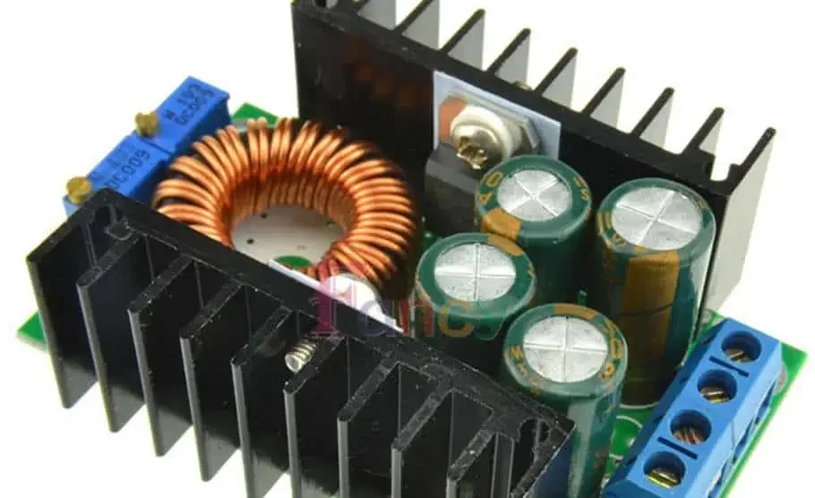
Define the input and output envelope
Specify input minimum, nominal and maximum at the converter terminals, including the source impedance and allowed transients. A bench supply set to a nominal voltage does not represent every cable, battery or upstream converter condition. On the output side, record continuous load, transient load, startup sequence, allowable ripple and the behavior required if another rail is already powered.
Select the controller using its operating range and control method, not only the largest voltage and current printed in a summary. Minimum on-time, maximum duty, current limit, light-load operation and compensation requirements can change the usable design space. An ideal duty-cycle result below 100% does not guarantee that a practical device can regulate at that operating point.
Choose switching frequency with component loss, size, measurement bandwidth and interference in mind. A smaller nominal inductor obtained by increasing frequency may impose different switching loss and layout demands. Keep a table of the worst input/load corners and the reason each corner matters. That table becomes a verification plan rather than a single attractive nominal calculation.
Operating points that answer different questions
| Condition | Review focus | Evidence |
|---|---|---|
| High input | Duty, ripple and switching stress | Actual controller mode and waveform |
| Low input | Dropout and maximum duty | Terminal voltage including source loss |
| Light load | DCM, skipping or reverse-current behavior | Exact control mode and observed output |
| Load transition | Feedback response and rail limits | Defined step and probing method |
Use the ideal CCM calculation as a bounded first step
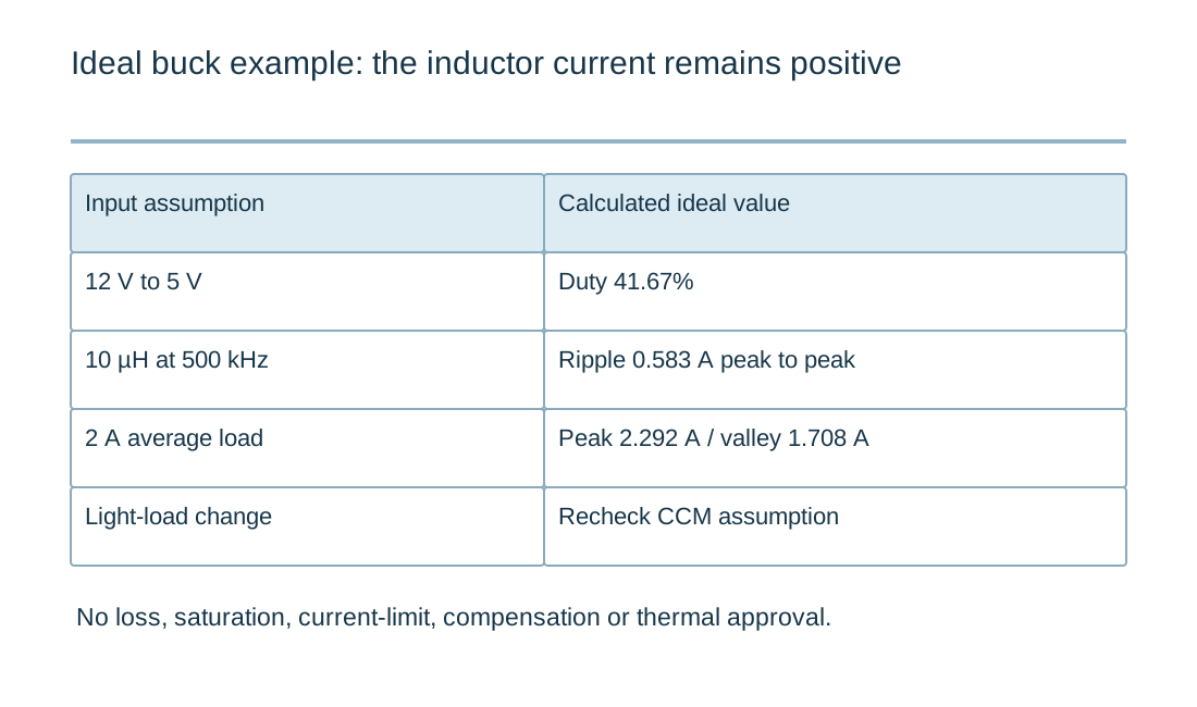
For an ideal fixed-frequency buck in continuous conduction, duty ratio D equals Vout/Vin. The inductor current change during the on interval is approximately (Vin−Vout)D/(Lfsw). With a triangular ripple, peak current is average load plus half the peak-to-peak ripple, and valley current is average load minus half the ripple. These expressions assume steady state, positive effective inductance and an ideal switching stage.
At 12 V input, 5 V output, 10 µH and 500 kHz, the ideal duty is about 41.67%. Ripple is about 0.583 A peak to peak. At a 2 A load, modeled peak and valley currents are approximately 2.292 A and 1.708 A. These are an arithmetic example, not a recommended design or a verified component rating. Inductance under bias can differ from the number marked on a part.
If the entered load is low enough to make the calculated valley nonpositive, the worksheet flags the CCM assumption. A controller with diode emulation, pulse skipping or burst behavior may operate differently. Do not use a negative ideal valley as a prediction of measured current in a mode that prevents reverse current. Device losses and practical duty differ from the ideal model as well.
| Review item | What to establish |
|---|---|
| Operating corners | Terminal input range, steady and transient load, startup and sequencing. |
| Inductor | Effective L under bias, peak current, saturation and winding temperature. |
| Current loops | Input high-frequency loop, switch-node area and direct return paths. |
| Feedback | Regulation point, compensation return and effective output capacitance. |
| Verification | Probe method, load steps, thermal boundary and controlled component substitutions. |
Ideal CCM buck ripple estimate
Ideal CCM buck ripple estimate
Use the current inputs and keep the assumptions
Load the example to inspect its units, then clear it before entering your own revision. Example values are deliberately labeled assumptions. Complete every field; an empty numeric input is not zero. Record the operating condition behind a value rather than copying the first number found on a component summary. For a comparison, keep the measurement boundary and units consistent.
Calculate after checking the inputs. Any edit invalidates the old result and disables its report download until you calculate again. An edited example remains identified as an example. Results and reports are generated locally without uploading a circuit or populating Contact. Attach the downloaded text manually if it helps explain the question. You can request a review directly without completing the tool.
| Input | What to establish before using it |
|---|---|
| Review reference | Nonconfidential revision label. |
| Input voltage · V | Evaluate input extremes separately. |
| Output voltage · V | Must be strictly below input. |
| Inductance · µH | Effective inductance under DC bias. |
| Switching frequency · kHz | Fixed-frequency ideal model. |
| Output current · A | Positive current at the modeled operating point. |
Place the input switching loop before routing everything else
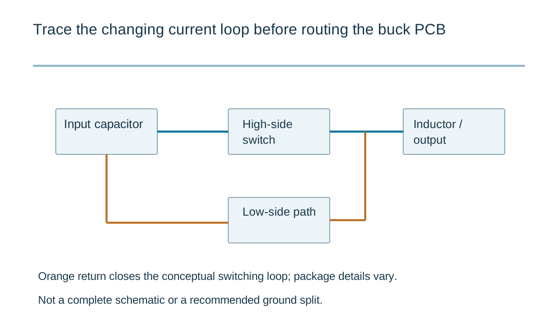
Follow the current in each switching state. The rapidly changing loop around the input capacitor and switching devices deserves particular attention. Place the appropriate high-frequency input decoupling according to the device reference layout, with a short, direct return. A capacitor electrically on the right net can still be ineffective if the physical loop is long and inductive.
Keep the switch node controlled in area and separated from sensitive sensing routes. More copper is not automatically better on a fast-moving node: it changes capacitive coupling and can distribute noise. At the same time, package thermal requirements may impose specific copper and via arrangements. Resolve these competing tasks with the selected component guidance and the actual stackup rather than a universal ground-splitting rule.
The output inductor and capacitor route carries a different waveform from the input hot loop. Trace both the forward and return paths and preserve the measurement reference for feedback. If the design includes an exposed pad, confirm its electrical connection and assembly treatment. Thermal vias, solder paste and void acceptance are manufacturing decisions that should appear in the release rather than being assumed from a schematic symbol.
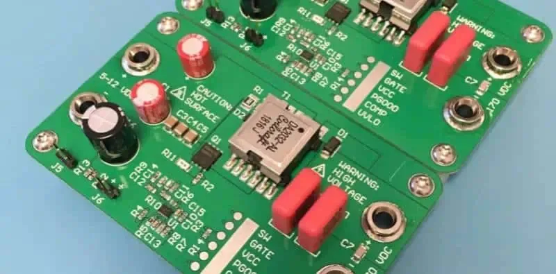
Give feedback a defined reference
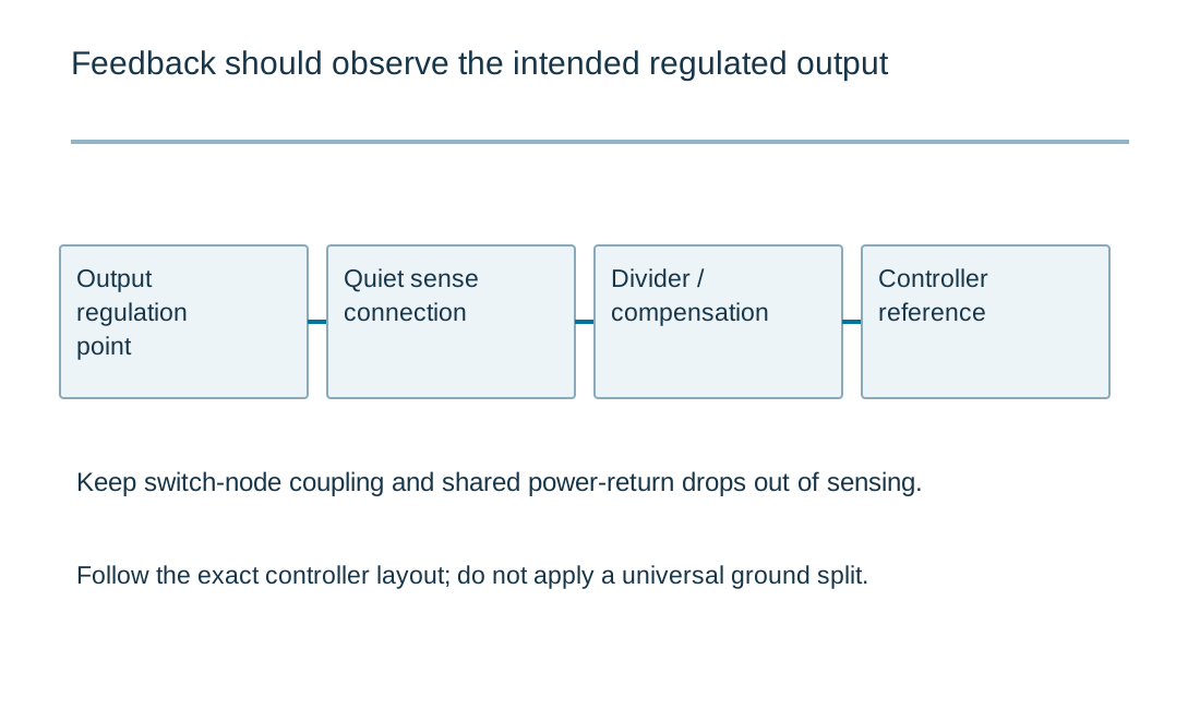
Take the feedback connection from the intended regulation point. A trace that shares a noisy return with a power current can make the controller react to the wrong voltage. Keep compensation components close to their relevant pins, follow the manufacturer's return guidance, and avoid routing high-impedance nodes near switch-node copper or fast gate signals.
Output capacitance is not only a ripple-filter choice. Effective capacitance under DC bias, ESR, load-step requirements and the controller's stability range all matter. A spreadsheet value that meets a simple ripple equation can still fall outside the regulator's supported compensation conditions. Record exact capacitor parts and the assumptions used to evaluate them.
For a rail feeding a current-regulated LED stage, distinguish the voltage converter's loop from the downstream current-control behavior. The LED driver circuit guide discusses string voltage and headroom. Cascading stages can introduce startup or dynamic interactions that neither stage's isolated nominal calculation reveals. Test the connected load, including its startup and protection states.
Measure ripple and transients at a declared boundary
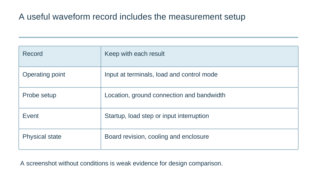
State probe location, grounding method, bandwidth and load condition beside a waveform. A long probe ground lead can create ringing that is partly a measurement artifact. Conversely, bandwidth limiting can hide a relevant fast disturbance. Comparing revisions requires a consistent setup, with the measurement method retained in the record.
Evaluate startup, input interruption, load application and load removal as separate cases. Observe the switch node and output with equipment and methods appropriate to their voltages. Thermal checks should run to an established condition in the intended airflow and mounting arrangement. A brief open-air bench run does not establish enclosure temperature or repetitive peak capability.
Include current-limit and recovery behavior in the agreed validation scope. The calculator cannot infer inductor saturation, MOSFET loss, diode stress, control-loop margin or electromagnetic compliance. Those gaps are not solved by increasing the displayed precision of its numerical result. Use the result to identify a question, then obtain the required simulation, measurement or component evidence.
Hand off an electrically and mechanically controlled revision
Provide schematic, PCB outputs, stackup, BOM, placement information and the test conditions that determine acceptance. Identify critical substitutions: an inductor with a matching nominal value may have a different saturation curve, and a capacitor with the same case code may have different bias behavior. Agree how substitutions are reviewed before assembly.
For a manufacturing inquiry, include quantity, finished construction and the inspection or programming tasks requested. If only a prototype review is required, name the uncertain operating corner instead of asking for a blanket assurance that the power supply works. The worksheet report can accompany those files, but it is not an automatic transfer to Contact and is not a released power-stage design.
Turn arithmetic into a controlled operating-point review
A converter has several different limits: voltage stress, current stress, magnetic behavior, heat, regulation and insulation where applicable. A favorable result in one calculation does not settle the others. Keep the input/load condition beside each result and identify the component evidence or test required to close the remaining questions.
Review the physical current path and measurement reference together. Layout parasitics can change switching stress even when nominal schematic values remain the same. A component substitution can alter inductance under bias, capacitor behavior, gate charge or loop response. Carry those dependencies into the BOM approval process and the test plan. A quotation should state what fabrication, assembly and verification are included, with unresolved design decisions kept visible instead of hidden inside a generic power rating.
Standards, source context and limits
Use the exact device revision and application conditions when applying manufacturer guidance. Reference designs are evidence about a specified implementation, not automatic validation of a modified board. Workmanship inspection, functional verification, product safety and application performance are different acceptance tasks. Public summaries do not replace the applicable licensed standards or a project-specific acceptance specification.
For fabrication scope and the agreed construction requirements, see PCB manufacturing.