What is wetting Soldering, Causes, and How to prevent them?

wetting Soldering

Poor solder paste wetting is usually an unseen cause of unreliable soldering processes and poor solder joints. Therefore, it does not imply that it is unavoidable just because bad soldering acts as a major problem. You can easily remove and prevent your board from occurring bad solder wetting and make the solder joints last longer with some tips and tricks.

What Is Wetting Soldering?

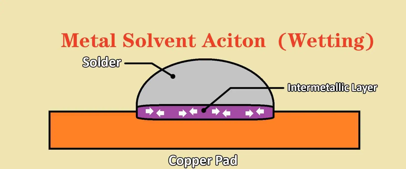
Soldering involves merging two metals with each other using a solder base or alloy. This type of technique is an old method of joining metals together permanently. At the same time, soldering wetting represents a type of process that bonds the metal with the solder metal over the surface of the PCB. During the process of wetting, the solder turns into a molten liquid, which attaches to the electrical components properly to make an adequate solder connection.

Adequate metal bonding or solder wetting needs a certain type of environment to commence this process properly. However, wetting needs a surface of copper that contains no contaminants and reacts with temperature properly. Here you can learn why adequate solder wetting acts helpful and how you can achieve success in this process.ย 

Why Is Good Wetting Soldering Important?

A good type of solder wetting requires metal joining in an appropriate manner. Without good solder wetting, metal does not attach completely, which also results in not passing the standard of the industry for proper usage. Thus, consider them generally defective. While proper and good solder wetting results in a proper solder connection that withstands the time of the test.

Appropriate solder wetting sees from it looks as it looks smooth and shiny solder which already reaches its max flow. On the contrary, poor or bad solder wetting is also visible. The solder turns porous, dull, and grainy, which shows its poor ability of adhesion. This type of poor solder may not be used in industrial settings as it only wastes time and money and reduces productivity.ย 

YouTube video

What Is Non-Wetting Soldering?

Non-wetting defects are a type of soldering issue that happens when the solder does not fit to make the bond with a PCB metal alloy. However, when the inability of bonding is not able to attach the terminals of electrical components and the pads of the PCB and give a secure connection. The surface of the board material remains exposed. At the same time, the solder itself resembles lusterless or giant. Moreover, non-wetting also causes voiding directly. It’s a process of creating holes within the joints of solder that may lack the materials of solder.

Wetting Soldering Vs. Dewetting

The defect of non-wetting differs from that of dewetting. Dewetting is a type of process that occurs when solder pastes coat the terminals of the components and pads of PCB but then leave some parts. This leaves thin solder surfaces on metal alloys and some thick and irregular clumps. The PCB surface material generally does not stay exposed all the time. However, whenever dewetting comes, it typically affects the joints of solder and filet quality first. 

Whereas non-wetting does not always but mostly occurs with solders that have no lead, for example, solder of copper-silver-tin. Some metals act promptly in non-wetting, while others donโ€™t because of the different materialization, as they have distinct spread and wicking features. Bare copper circuits with preservatives of organic solderability are sensitive to the PCB pad’s non-wetting, particularly if they pass through more thermal cycles. Whereas pure tin offers well spread and minimizes non-wetting. Same as silver immersion surface finish work. Gold-and-nickel alloy also solders properly and reduces the non-wetting as long as they do not have any impurities.

Importance To Fix Non-Wetting Defects of Soldering

Non-wetting results in causing severe issues of structure that affect the performance and function of the board. This causes poor solder joints over the PCB surface. However, poor solder joints on the PCB break easily, which results in poor conductance of electricity. Moreover, when solder paste does not attach to the PCB pads, components, and the metal of the base, it may lose integrity and make food joints or may come off either quickly or be subjected to stress. Also, improper components connections affect the functionality of the PCB.

Common Causes Of Non-Wetting Soldering Defects

FULL PCB MANUFACTURING Quote

The defects of non-wetting are caused because of many reasons. Here are some practical reasons for occurring non-wetting over the surface of PCB.

1. Inadequate PCB Finish

The circuit board’s surface finish determines how much wetting causes and how well a solder paste reflow. However, if PCB boards have an inadequate surface finish leaving the board bare, it makes it difficult to reflow the solder and may stick poorly on the PCB.

2. Improper Pin Platting

If PCB copper pins receive improper copper plating before going through lead/ tin plating. However, it may become sensitive and cause non-wetting. This is because a sufficient amount of copper plating plays a vital role in keeping zinc from intervening with lead or tin plating. Thus, keeping the solder paste from attaching properly.
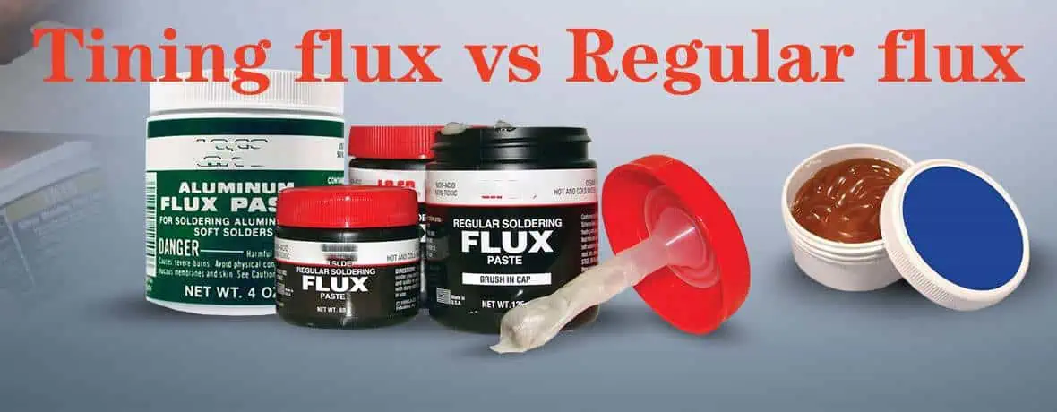
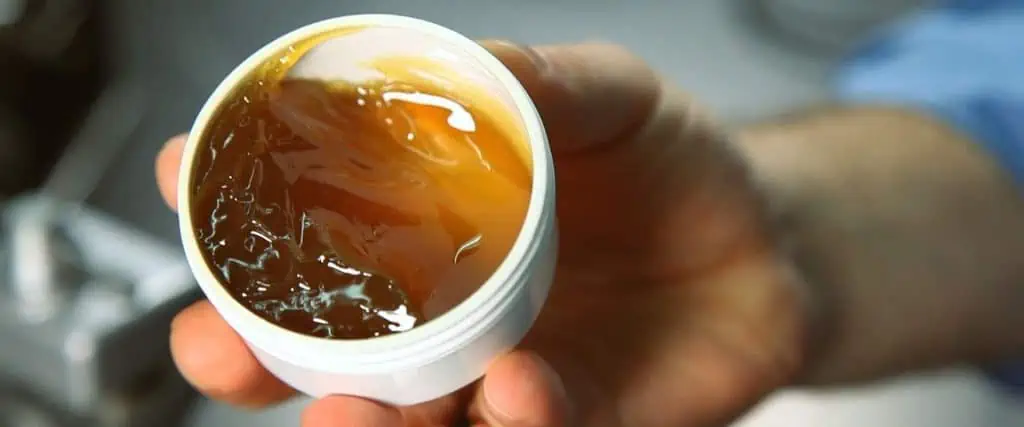
3. Degraded Flux

Degraded or old flux, a cleaning agent with chemicals used after and before soldering, can cause non-wetting. Moreover, flux degrades faster in a container with an opening. Although, even if the solid residue stays intact, it may diminish its performance subsequently. Therefore, a regular type of flux serves as helpful in this case.

4. Wrong Type Of Fluxx

The kind of flux you use for cleaning also depicts whether it causes non-wetting on the surface of the PCB or not. Generally, fluxes with high-activity results in adequate solderability and reduce the risk of non-wetting. On the other hand, fluxes with low residue and low activity remain inadequate to clean the oxides and residue from the PCB surface. Thus, these oxides may interfere in causing wetting.

5. Incorrect Lead/Tin Times

When PCB contains a very thin layer of lead and tin plating, any incorrect thickness may result in non-wetting and solderability. Nevertheless, the thinner plating layer possesses short life and does not survive longer until the process of soldering occurs.

6. Long storage Times

If the PCB stays too long in storage, it makes soldering difficult, which causes non-wetting. Although, solderability typically fits directly to the thickness of the plating. However, during a long stay in storage, it may break the good solderability of the necessary plating. A PCB which remains in storage for over a year or maybe more is at higher risk of non-wetting and poor solderability. 

7. Poorly Applied Board Resin

If resin spots on the surface of the PCB, it reacts with soldering, which results in non-wetting. For instance, the resin of the board can spot over the edges of pins, which results in non-wetting only in those specific areas.

8. Problems With The Bath

In some scenarios, non-wetting is produced across the coating of the PCB. For instance, a coating of gold surface finish on the circuit results in non-wetting throughout the board due to the imbalances in the bath of electroless gold.

9. Oxidation

PCB oxidation which receives soldering, results in non-wetting. The intervention of oxides, the base substrate, and the solder prevents adequate adhesion. This results in creating non-wetting all over the PCB surface and makes it oxidize.

10. Insufficient Solder Paste

A solder paste with low volume may constantly result in non-wetting. A good solder paste spread seems essential for creating stable and reliable solder connections. However, when the assembly of PCb uses solder paste in less amount, it may not create a proper adhesion connection between the boardโ€™s base substrate and the solder. Therefore, sufficient or an adequate solder paste amount causes wetting of around 100% on the surface of the PCB.

11. Poor Choice Of Solder Paste

Solder paste plays an important role in preventing non-wetting and works better than others. Typically, along with fluxes, a solder paste with high activity affects more than a solder paste with low activity. It minimizes the non-wetting risks and enhances the solderability.  

12. Expired Solder Paste

If PCB solder paste surpasses its expiry date, then it may not adhere as strongly as it did before because the flux does not activate sufficiently to eradicate oxides or contaminants from the surface of the board for better wetting and solderability.

13. Insufficient Soldering Temperatures

Too low soldering temperatures tend to encourage non-wetting over the PCB as solder needs a level of the thermal threshold for bonding adequately with the metal substrate. However, if somehow the soldering temperature does not surpass that threshold, then the solder paste does not attach properly to the pads of the PCB or the PCB components. This issue usually arose in lead-free bases, which usually possess high melting points as compared to the alloy of lead or tin.

14. Inconsistent Soldering Temperatures

Fluctuating or Inconsistent soldering temperature may cause non-wetting over the surface of the PCB as they forget the flux activation process and provide poor solder adhesion in some areas of the PCB. However, if specific problem spots over the surface of the PCB do not get the heat that already reaches activation temperatures of the flux, then the solder paste may not adhere to those specific areas as it needs to.ย 

15. Short Soak Time

SMT-Through-Hole-Soldering

The time duration a solder paste stays over the circuit directly impacts the ability to make a bond with the metal substrate of the circuit’s surface. Moreover, when there is not sufficient time to attach the solder properly, it leads to non-wetting within the board or certain parts of the board.

16. Long  Soak Time

On the other hand, if the soldering paste stays long enough on the circuit during the process of reflow, the excess time may tire out the PCB flux before the process of soldering. However, if PCB flux turns inactive due to the excess soak time, then it rises the non-wetting subsequently.

17. Solder Paste & Plating Material Mismatch

If the material of the metal plating layer and the solder paste type are incompatible, then the soldering paste becomes ineffective for stimulating links between circuit pads and components of the surface.

18. Smaller Chips

Smaller chips comprise thin solder paste layers. In such scenarios, the solder paste layer may not allow sufficiently for whole PCB prop-wetting.

19. Contaminated Flux Or Solder Paste

Solder paste in contaminated flux does not connect components or clean the circuit effectively and also approves sufficient wetting. The contaminants can also leave undesirable residues over the surface of the circuit. Tintervenesvene with the flow of solder and results in non-wetting.

Preventing Poor Solder Wetting During Reflow

Various steps help in improving the wetting performance. However, these steps do not always work. Therefore, choose the method that suits well for your PCB design

ยท Higher Activity Solder Paste

This provides better wetting, particularly for soldering tough surface finishes and oxidized surfaces. 

Selecting a distinct type of solder paste drastically affects the wetting efficiency. Therefore, we provide a waste range of solder paste that falls perfectly for the unique needs of manufacturing, along with enabling maximum wetting.

ยท Minimize Oxides 

You may also choose less-oxidized PCB surface material. This may seem impossible to work. However, you may also work with nitrogen along with the high-activity paste during the reflow process. This aids in reducing the oxide level that is created during the process of reflow.

ยท More Solder Paste 

An efficient way of fixing poor wetting issues is to alter the stencil. This helps in using the solder paste with increased volume. If additional solder paste doesn’t work for you, then choose larger lead components. This allows reimbursement of low-volume solder paste and enables the solder connections to complete. 

ยท Adjusting The Reflow Profile

Enhancing the soak time helps you in equalizing the temperature of the soldering process and removes the problem areas. This allows a reasonable wetting for both the component leads and the pads. However, enhancing the time beyond liquidus aids in enabling the complete liquid flow of solder in liquid form before it starts freezing.

Guidelines for Interpreting Ionic Contamination Testing

ionic contamination testing

PCBs are huge assets for the fine performance and longevity of consumer electronics and futuristic smart devices. However, things can go south with PCBs due to ionic contamination.

 The contamination of PCBs normally occurs due to faulty fabrication and external factors. Now, these external factors can be anything. From flux remains to extreme weather exposure, such factors create a negative impact on PCBs. 

Nevertheless, there are some viable solutions to save PCBs from all such threats. It includes ionic testing of PCBs. The purpose is to detect the contamination first before coating the PCBs. There are many benefits of this checking method. We will learn about the ionic testing of PCBs in detail. 

WHAT IS THE Ionic Contamination Testing?

Ionic contamination means that the fragments of the flux are still remaining on the PCB surface. It normally occurs when you are assembling the PCBs. However, it has consequences as well.

 There are unbreakable electrostatic bonds between ions. These bonds can either be positive or negative. A fine example is Sodium Chloride, aka table salt. The sodium ions are positive, while chloride ions are negative. 

The PCB parts have their own ionic residues that can damage the PCB later. These can be:

  • Corrosion-resistive substances
  • Oils and liquids
  • Biocidal entities

Not only this, but some non-ionic factors are also not healthy for the longevity of PCBs. These are oils used for the assembly process and molds. You cannot predict the contamination of PCBs at all. It can occur at any place and can lead to extreme damage.ย 

Ionic Contamination Testing for Cleanliness Prevents Issues 

ionic testing
ionic testing

As you know, flux has great importance in PCB assembling and its performance. You can rely on different types of flux for this purpose. These different types of flux are also beneficial for soldering. However, with each flux type comes contaminants as well. 

Some of the common flux used in the process of soldering are:

  1. Resin (Rosin) Flux: It includes abrasive and non-abrasive fragments
  2. Organic Flux: It produces removable residues that can be corrosive, and some can be less abrasive
  3. Inorganic flux: Leaves extremely corrosive residues

Procedure of Ionic Contamination Testing – Plasma

Ionic contaminants can cause huge damage if not treated properly. These can also retard the fine performance of PCBs. Due to this reason, contamination checks are important to ensure everything is in place from time to time.

 You can use some special tools like a contain meter and omega meter for this checking method. These tools are helpful in detecting ionic cleanliness. You just need to add some ions into a special liquid that will give the precise amount of ions present based on the criteria of ions of NaCl. 

Advantages of PCB Ionic Contamination Testing

Now, you know why performing such checks is important to enhance the performance of PCBs. However, in the past days, manufacturers would use conformal coatings for the same purpose.

 Although they had high hopes for these coatings, they did not remove the contaminants completely. The purpose is to leave not a single fragment on the PCB surface. 

If you leave any residue unknowingly, it will lead to irreversible contamination. It will also invade new coatings afterward. Now this verification method also helps you remove the non-ionic fragments. Some major benefits of this process include:

  • It completely excludes the invasive ionic fragments produced due to the soldering of PCBs
  • Besides, it also comes in handy for boosting the ionic cleanliness of PCBs before you bring them into contact with any sort of coating.
  • It removes the non-ionic invasive entities from the surfaces, ensuring 100% ionic cleanliness of PCBs 
  • Besides, It is an affordable method and delivers positive results.
  • It is not time-consuming as it just takes 24 hours for the completion.

Ionic Contamination Testing In Different Industries

The ionic contamination test is an important verification method for different domains. It is crucial for thorough testing of PCBs so that they can perform efficiently under extreme conditions. 

Also, it protects the PCB parts from undergoing future damage. Not only this, but this testing also ensures that the data stored in your setup is safe on all counts. The fields that never compromise ionic contamination testing are: 

  • Solar energy sector
  • Aerospace 
  • Defense and military
  • Computing industry
  • Medical/healthcare sector

Problems arise due to Ionic Residuesย 

FULL PCB MANUFACTURING Quote

Below are the issues that arise if you do not ensure 100% ionic cleanliness throughout your PCBs:

  1. CorrosionCorrosion mostly invades the metallic PCB parts when there are ionic entities still present on the surface. Ionic contamination can lead to corrosion in just a short period of time. 

In order to make sure the PCB parts do not undergo corrosion, this test is inevitable. Also, moisture can lead to short circuits and electrical faults when it interacts with ions. The metallic surface slowly starts to crumble and hampers the performance of PCBs.

  • Dendritic growth: It means an unusual build-up of metals starts to grow on the PCB surfaces. Dendritic growth is due to an electrolytic substance formed due to DC voltage bias. 

Metallic dendrites result from the left-out holes of a solder cover. Now, this solder cover would contain flux residues and other ions. If these dendrites combine with each other, it will lead to electrical failure, electrical fire, and other issues like short circuits. 

  • Electrochemical migration: Electrochemical migration normally occurs due to the dendrites that form on a dielectric substance. These can contain conductive ions. Now these ions can re-route the current from its passage. Electrochemical migration is a major threat to the life length of PCBs. 

Ionic Contamination Testing And Cleanliness Measurements

There are some important measures for ensuring complete ionic cleanliness other than ionic contamination testing. These are equally important to boost the longevity of PCBs. We are going to discuss these in this section for better understanding!

  1.  Resistivity testing: There is a special resistivity testing tool that is important for ensuring the cleaning of PCBs. However, it does not mean that it will provide desired results since the cleanliness of PCBs should meet the IPC criteria. 
  2. ROSE test: ROSE testing is to identify the invasive ions that can cause problems to PCBs. It is beneficial because the ROSE test sketches the ions that are present. Now, it is much easier to detect these ions due to clear visualization. 
  3. Modified ROSE test: The modified ROSE test is helpful because you can use it for thermal extraction as well. It just exposes the solvent to extreme temperatures. An ionograph gear is reliable for performing this test. 
  4. Ion chromatography test: An ion chromatography test is also helpful for excluding all the ionic content completely. The test includes passing the solvent from ion chromatographs which makes this test highly important among the others. When you get the results, it will show what ions are still active in the solvent under observation.

Effects of Ionic Contamination and Testing in a PCB

By far, you are well aware of the adverse damage caused by ionic contamination. The PCBs can undergo extreme damage due to this type of serious threat. Before the production process starts, the raw boards might have flux remains, traces of etching chemicals, and solder fragments. 

There is no margin to leave these substances on the boards due to the worst consequences. 

  • Electrochemical migration (ECM): Electrochemical migration happens when the entire metal disappears due to the electric field. It gives rise to ions between two metallic electrodes. Not only this, but it also initiates dendritic growth when ions interact with electrodes. These dendrites occur due to conductive ions. It is the main reason for adverse damage to PCBs and electrical glitches. 

Ionic contamination is not the only culprit here. There are some other factors that have the potential to damage PCBs as well. These are environmental conditions and exposure to extreme temperatures. 

It is recommendable to first bake the PCBs to remove all the moisture. You can even use a controlling tool to prevent ionic contamination. It is beneficial to make sure that all the steps of PCB production are accurate.ย 

Choosing RayPCB For Ionic Contamination Testing

RayPCB experts believe it to be highly tolerant of ionic contamination. Since ionic contamination is a budget-friendly and affordable test, plasma just adds up to its significance for major PCB producers. The ROSE test is also beneficial for the ionic cleanliness of your PCBs. Such tests for ionic contamination are not a threat to the environment as well. 

Also, you can take help from this test to see what type of cleaning technique fits well with the PCB you are assembling. There are some important things to remember after completing the test. 

We make sure to re-detect the PCB parts for ionic content. Our purpose is to provide you with industry-grade expertise so that your PCBs can serve you well in the long run without any hustle. 

What are the Factors Affecting the Cost of Electronic Manufacturing Production?

pcb assembly cost down

Youโ€™ve just created a perfect idea for your new electronic products. Thatโ€™s great because I understand what it feels when you get a positive inspiration to achieve something. However, before you start spending so much on getting this idea developed, I advise that you focus much effort in estimating the cost required for the development of this product.

More importantly, thereโ€™s a need to estimate the amount it costs for the mass production of these products. Donโ€™t make the great mistake of having an underestimate of the costs or not having an estimate at all. This is because to succeed in the market, you have to know the necessary costs upfront.

Costs involved in Developing an Electronic Product

The cost for development for the majority of hardware is usually broken into three main categories. These include plastic with other mechanical components, electronics (which includes programming), as well as retail package. The mechanical parts help in holding the products together, while retail package aid in the protection and selling of the product.

Software and Electronics

Usually, electronics are the most expensive and complex part of a product to create and develop. This is composed of two main parts. These include the design of the PCB and the programming because the majority of products need some programming.

The prototyping of these electronics can be divided in two steps. These include producing the blank PCB, as well as the soldering of the entire electronic components to the PCB. Furthermore, the PCB can be regarded as what holds together and connects each electronic component.

The amount of development cost for the PCB design of electronics compared to the software usually varies. This depends on whatever product you are working with. Also, for the majority of products, the split between both is equal.

However, the majority of products could swing towards becoming more software-complex or hardware-complex. The required costs follow accordingly. Most times I recommend beginning with 3 โ€“ 5 boards, after which for every iteration, you can increase the quantity.

Immediately you have confirmed the functionality, as well as calculated the majority of major bugs, then the quantity of the prototype can be increased and then the samples can now be shared between potential customers and investors.

Mechanical Parts and Enclosure

How To Cut PCB Assembly Cost While Maintaining Quality

Some type of plastic enclosure will be required unless the product would be strictly marketed by a DIY/maker market. Expect that youโ€™ll have to spend a minimum of some thousand dollars to create 3D models for this enclosure. When the ergonomics and appearance are important for the products, then the 3D model design costs will be more.

Some products might need extra mechanical parts like stamped metal parts, as well as moving parts. It will include extra costs for prototyping and mechanical engineering. Plastic enclosure prototyping can be achieved making use of 3D printing tech. This 3D printing creates a part that is custom shaped through the stacking of layers of the molten plastic.

This 3D printing popularity has really assisted in bringing down the creation cost of the plastic prototypes. Buying a personal 3D printer might be a very cost-effective strategy for several startups. For some products, there is a technology referred to as CNC machining, which might be the preferred option compared to 3D printing. In contrast to 3D printing that is viewed as an additive process, the process of CNC machining can be viewed as a subtractive process.

Rather than stack layers, just like 3D printing, the CNC machining is just like sculpting. This process begins with the removal of a block of material and plastic to create a final shape. CNC machining has the major benefit of allowing the utilization of manufacturing injection-molded plastics whereby, 3D printing utilizes unique prototyping plastics, which might have a unique strength, feel, look, in contrast to the injection molded or production plastic, which would be used ultimately.

Development of the Retail Package

Majority of the hardware entrepreneurs donโ€™t pay importance to the development of the retail package. Note that this oversight is a major one that comes with grave consequences. Furthermore, unless you want to sell this product online, this retail package shares a similar significance as the product. At times, it is more important.

If the retail package of the product isnโ€™t conveying the right message to the customers, even if it is the best product globally, it will never sell. Take note that, without sales, nothing matters. Generally, two retail package types are utilized for the electronic products. These include boxes and clamshells. The smaller products are usually packaged into clamshells, whereby larger products usually favor the retail boxes.

Retail boxes and clamshells are usually composed of two main pieces. This is a plastic piece (custom-shaped) that protects and holds the product, as well as a piece of cardboard artwork that conveys the sales message.

Just like the enclosure of the product, the packageโ€™s custom-shaped plastic part will need you to develop a 3D model. After this, an injection mold would have to be bought.

What is the Cost of Electronic Manufacturing Production?

FULL PCB MANUFACTURING Quote

 This cost of landed production is the eventual cost of the product when it lands in your warehouse. For sure, the cost of landed production is the most significant cost. This discloses the cost of inventory, the amount your products can be sold, as well as the amount of profit this startup will make.

In addition, in contrast to the scaling and development costs, this cost is one you will continue to face so far the company exists. This landed cost of production explains the whole cost required for the production and transportation of one unit to the warehouse. Below are some of the things to consider when asking the question: โ€œwhat is the cost to manufacture a new product?โ€

Electronic Components

The cost of electronic components would be the hardest to properly determine when dealing with an electronic hardware product. This is due to the fact that considerable work on engineering design is important to know the components that are needed for the product.

Also, determining the needed electronic components for new products need considerable efforts in engineering. Many startups usually wait till the product has been completely prototypes and designed before determining the cost of their component and then finally the cost of production. Now, this is wrong, because there is a need to get your cost estimate ready before spending money developing your product.

Printed Circuit Board

Like your prototypes, manufacturing electronics takes two steps. First of all, the bare PCB is manufactured, then all electronic components would be soldered to the circuit board. Cost of the bare PCB is usually determined by the size as well as the routing layers. Two layers of routing (the bottom and top) at least are required.

Moreover, majority of design would need between four to six layers. Designs that are more complex might need at least eight layers. Raising the number of layers in general would allow the reduction of the printed circuit boardโ€™s overall size.

The cost required for assembling the PCB is mainly determined by the least pin pitch, number of parts or components, the utilization of the leadless packages like BGA or QFN, as well as if the soldering of the components is done on the two sides of the printed circuit board.

PCB assembly is usually done through automatic placement machines. Take note that the cost involved in the production of the assembled printed circuit boards in volume will be much cheaper compared to the cost of each prototype (unit cost). Majority of this cost is seen in the initial setup; therefore as there is an increase in volume, the cost of the setup becomes minimal.

Plastic Parts (Custom)

The cost paid for every unit of production for the plastic pieces can be mainly determined by the mold time, size, weight, and plastic type used. Each pieceโ€™s weight and size depends on the design, therefore you can do very little to control the variables for making a smaller product and less durable.

Eventually, you may raise the speed of production and reduce the cost of the parts by making use of many cavity molds. The injection mold (multi-cavity) allows the manufacturing of multiple copies of parts having single plastic injection. However, having several cavities would increase the cost of the mold significantly.

Now, donโ€™t just start buying many cavity molds till you have been able to work through all changes or tweaks to the initial molds. Also, before upgrading into many cavity molds, it is advisable to run some thousand units. Increasing the mold cavities is the most reliable option for reducing the cost of the plastic parts since the plastic type, weight, and cost impacts the end products directly.

Other mechanical components

Several products will need different components like metal pieces that are stamped (for the internal shields), screws, gears, springs, motors, etc. In so many scenarios, the stock components are useful which would get rid of all scaling costs.

Product Assembly

Immediately you have the individual components ready, assemble them so as to form the final product. This stepโ€™s cost is completely labor costs. What this means is that you will have to complete the assembly at locations having low wages like Asia. The final assembly cost of the product is majorly labor costs.

Testing of the Product Quality

Immediately after assembling your final product, then there is a need to test it so as to confirm that it is very functional and meets quality specifications. In addition, there are some electronics testing that must be conducted before the completion of the final assembly.

Not testing properly, or shipping of bad units is a well-known error, which could being death for any startup. A good number of entrepreneurs usually rush their newly-created products to the customers, however shipping of bad units would give your company a bad name right from the beginning.

Manufacturing Scrap

There is no perfect manufacturing process and you can be sure to have faulty units. At first, it might be at least 10%; however, with time, you can optimize the process of manufacturing. With this, you can reduce the number to just one to three percent.

Shipping and Retail Packaging

Costs of packaging have to do with if your product would be selling primarily online or at the retail stores. For products that are sold to retail outlets, then it is very important to have the best retail packaging. This will make the costs of packaging significantly higher.

Also, the cost of packaging could be highly reduced if you decide to sell your products strictly online through industrial customers or TV. The high end type of retail packaging could be very expensive, with every package costing around five to ten dollars. This is why it is advisable to begin with a simple packaging to help reduce your costs. It is one of the main reasons why focusing on online sales initially is best.

Also, remember to add the master cartonโ€™s costs used for shipping the packaged product. In addition, the cost of the master carton is usually low but still it has to be included in the cost calculations. When the product needs a stand for the retail display then that would be able to include a different cost to the cost calculations of your package.

Product Returns

The same way you are sure of having some units that are faulty and which you must scrape, you are also sure to have some unhappy customers who wish to request a return. Therefore, ensure that you include this in the final cost of production.

Just like scrap rate, the return rate has to decrease when you optimize the product, customer service, and packaging.

Logistics and Shipping

Majority of products are produced in Asia. What this means is that the completed product will have to be transported from your factory to a local seaport. After this, it would be loaded onto the cargo boat to be shipped to the country of choice.

Immediately this boat gets to your country you have to truck it to the warehouse. You can also send it directly to the customer.

Container Boat

PCB assembly cost breakdown

Majority of products that come from Asia are usually shipped through the sea on large container boats. There are rare cases where you might wish to ship through air cargo; however, the cost would be much higher. For truck shipping, the weight determines the cost of shipping, while for boat shipping, the volume plays a major role in determining the cost.

Tariffs, Duties, and Taxes

Remember the taxes. The manufacturing company and the importing country would charge duties that have to be added into the eventual landed cost. Though, some categories of products might be exempted from the import and/or export taxes.

Every classification of a product comes with a HS code. Immediately you are done determining your productโ€™s HS code, then you may consider the import and export duty rates.

What Factors affect the Cost of Electronic Manufacturing Production?

Costs of labor

Costs of labor usually vary according to the regionโ€™s socio-economic costs where the work has been performed. The customer usually wants the costs of labor to be very low, and at times this could be achieved without affecting the quality of the product.

This is the case when the process is very automated or whenever you are performing basic tasks. For such cases, you donโ€™t require great skill; therefore you donโ€™t have to pay for this. Moreover, searching for the lowest costs of labor alone isnโ€™t a good investment during new product development.

Raw Materials

The first moves that the product developers have to make is the type of materials to make use of. Sure, you have thousands of metal alloys and plastic resins to select from. All of them come with their own physical properties. They also come at different points in price.

The great news here is that the expense is the easiest to control and predict. This is due to the fact that commodities and raw materials are traded widely on the global market. This cost, with a few exceptions, has to do with the volume of the material consumed and wonโ€™t vary a big deal no matter the place manufacturing takes place.

In addition, finding the commoditiesโ€™ price tables on the net comes easy and they are usually updated therefore the developer can account for it beforehand. Though we donโ€™t advise the use of substandard materials, we advise that the developers of the product work with materials that adhere to the functional requirements and needs.

Part Complexity

Remember that the complexity does not usually improve the performance or look of the product. In fact, the very complex designs could hinder the performance and utility of a product coupled with its expensive nature.

Also, take note that measuring the complex feature could be extremely time consuming too. It might also need special gauges or fixtures to measure the complex shapes, which adds to the overall cost as well. Generally, itโ€™s advisable to design the part to become complicated the way it should be.

Tooling

Processes requiring specialty tooling involve high-pressure die casting, plastic injection molding, as well as polyurethane vacuum casting. The preparation of these tools could take weeks, and this might represent a huge initial investment.

This is why much care has to go into the design. Three major inputs are responsible for the cost of these tools. These inputs include the materials from which these tools are manufactured from, if they need special treatments such as photo etching, surface coatings, or heat treatment, and their complexity.

Volume

A toolโ€™s price canโ€™t be avoided because of its importance. Moreover, if it has a high volume, this tool cost would become negligible since producing each part comes at a less expensive price. This is one reason why we advise investment in reliable tooling materials when there are large expected volumes.

Tools that are more expensive could be cycled faster, hold tolerances that are tighter, become more durable, and create less scrap parts. Donโ€™t choose cheap tooling if the investment is justified by the volume.

Also, another consideration here is that the suppliers of the raw materials can at times provide discounts when a bulk purchase is made. You have to consider this for the lifetime of the product, and not just one production order.

Precision

This is a term usually confused with accuracy. However in the manufacturing world, both concepts have a slightly different meaning. Accuracy deals with the closeness of a featureโ€™s measurement to the true values one strives to achieve. Also, this could be a micron, meter or an inch, since accuracy is usually indifferent to the measurementโ€™s system being utilized. Whatever this nominal value is, when you are closer to create a feature for the value, then you have become more accurate.

Precision means that you are accurate at all times. This has to do with repeatability with different acceptable tolerances, which are away from its nominal value. Numerous product developers do not realize that higher accuracy and precision degrees require investing more effort and time. This additional work needed increases exponentially as the tolerances become more refined.

This is due to the fact that all the raw materials can be affected by humidity, temperature, as well as several environmental conditions. Also, they deflect and move under pressure of the clamping forces and cutting tools. These facts are fundamental and cant be avoided. Considering the larger scale, they are imperceptible movements and can be accepted easily.

Conclusion

The necessary cost for launching new electronic products could be overwhelming, most especially for startups and entrepreneurs. The costs of development would be an obstacle to avoid, and the costs of scaling would become the highest cost. Moreover, the cost of landed production would be the most significant cost because it tells the inventory cost, sales price, as well as the profit.

You will then move beyond all scaling and development costs. However, you will need to accept the cost of production indefinitely.

Why Upverter PCB Design Tool is a Preferred Choice among PCB and Electronics Designers

motherboard pcb design

Upverter is a quick and easy-to-use software design tool. It is the most professional and easiest software to design innovative circuit boards and electronics. Engineers and PCB designers make use of Upverterโ€™s PCB layout editors and schematic capture due to the features it offers. Upverter provides a wide range of unparalleled innovative features that help you enjoy your PCB design workflow.

What is an Upverter PCB Design Tool?

Upverter is an online PCB design software specially made to offer integrated and advanced PCB design. It is a modular PCB design tool for designing and ordering circuit boards according to your exact specifications of IoT devices and hardware. With this software, you can experience the simplicity and creativity of customizing and developing a board.

Upverter PCB design tool allows hardware engineers to design and review PCBs and schematics. Also, it is capable of generating a bill of materials (BoM) and Gerber files. This PCB design software is equipped with web-based tools that can edit schematic diagrams and as well lay out circuit boards. There are several benefits of using Upverter. One of such benefits is that users donโ€™t need to pay for ope-source projects in this online PCB software.

Asides from designing PCB layout and performing schematic capture, Upverter performs design review, version control, and issue management. This PCB design platform offers support to import from OrCAD and Altium file formats. Also, Upverter PCB design software offers a comprehensive library and collaboration features.

This easy-to-use and professional web-based tool offers a wide range of features which help in making PCB design a great experience. In 2010, Upverter was specially created as a web-based EDA tool for hobbyists, open hardware circuit designers, and students. The success achieved in creating Upverter is a stepping stone for other web-based EVA tools like EasyEDA.

The majority of EDA tools provide free version for project makers and hobbyists. Upverter is a good example of such tool. This professional tier provides more advanced features such as API, 3D preview, BOM management, and CAM export. Furthermore, Upverter is an easy top-tier EDA software you can easily learn how to use, thanks to its highly-intuitive user interface.

Characteristics of Upverter PCB Design Software

Designspark PCB library

Verified parts database

Upverter features a verified parts database. Users donโ€™t need to design the footprints or schematics for the majority of the common parts. The parts search is good enough.  The verified parts of Upverter is a great way of taking off the burden or trouble of double checking every component.

PCB layout tools

The PCB layout tools of Upverter are very easy to use. If you are first time user of this tool, you will find it very easy to integrate these tools. With the PCB layout tools in Upverter, users can change between imperial and metric system. Also, they provide default values for the traces and vias which makes it easy to design complex multilayer PCB designs.

However, the PCB layout tools donโ€™t include the auto trace feature. Upverter wonโ€™t provide this since their model is to provide PCB layout for hire.

Collaboration

One of the best characteristics of Upverter PCB design tool is that it enables users to work with others in the same design at the same time. For example, two users can use the same schematics. Upverter is a collaborative tool in the electronics industry. This software allows you to invite several collaborators on a project and work together in real-time

Upverter Pricing

The Upverter PCB design tool comes at a professional price. Although there are much better PCB software tools, there are several businesses designing products with tools whose pricing ranges between $500 to $1000 per seat for a year. The Parts Concierge service is a competitive advantage for Upverter. With this service, you wonโ€™t need to create any part from the beginning again. Upverter is integrating a combination  of slick scripts to pull off part layouts from a datasheet.

Creating a Schematic in Upverter

There are three things you need to carry out in Upverter. First of all, you need to recreate a schematic, secondly, you will be making a part from scratch. Finally, the schematic will be transformed into a board. The main focus of Upverter is that you donโ€™t have to get worried about part libraries. There are several datasheets and footprints. When creating a part in Upverter, ensure you edit the characteristics of the part. These characteristics include a link to a datasheet, part number, and manufacturer package.

After this, the generation of pins for the schematic symbol is the next step. In the toolbar, select the โ€˜Pinsโ€™ label and click the edit button, you will see the Pin Manager dialog displayed on the screen.

PCB Layout Using Upverter

FULL PCB MANUFACTURING Quote

Before the PCB layout, you must have designed your schematic. To layout a board using Upverter, you need to use the PCB editor button located at the top of the page to switch to the PCB view. Your circuit board will be displayed on the screen. Below are steps in PCB layout process using Upverter

Set the board size and place component

The first thing you do is to ensure your PCB size is set. After this, open the inspector by double-clicking the background. Set the size of your PCB. Select save and close the dialog.

Route traces

Click on the trace tool on the left side to draw a trace. In the process of drawing the trace, click on space to ensure the trace angle is switched. After this, you will have to place the traces between the pads linked with red lines to ensure the circuit is complete.

Pours

Since the circuit board is now routed, you will need to fill the empty space by adding a pour. To add pour, select the pour tool at the left side and draw a square shape around the circuit board. After you have completed the pour, press the esc button. Open the pour inspector by double clicking the pour outline.

Layers

 You will be using the layers panel to choose the layer you want to work on. Also, you can make use of vias to route between layers. You can route a trace to carry out this task and change to the bottom copper layer. With this, you have create a via automatically.

Silkscreen text

The silkscreen layer is an important part of a PCB. It is always printed on a circuit board. Also, this layer makes the circuit board very easy to comprehend. The silkscreen layer has no negative effect on your circuit boardโ€™s electrical properties. Press โ€˜tโ€™ for placing silkscreen text and click the area you would like to place the text. Input the text in the text box.

Why Choose Upverter

  • Upverter PCB design tool allows hardware engineers to design and review PCBs and schematics. Also, it is capable of generating a bill of materials (BoM).
  • Its intuitive and simple user interface ensures it is easy for users to easily master within minutes. Also, Upverter is a great option for newbies in electronics design.
  • It allows you to design a project in a matter of few seconds, pick parts and then connect them together in a schematic.
  • You can easily sign up with this software as the process is smooth and quick. Also, you only need a few minutes to run. With only few clicks, you can import an existing project.
  • Upverter offers efficient parts library which makes it easy to save tome while improving the finished design. This software is a great choice for creating hardware.
  • This software offers everything required to transform your creative idea into a physical prototype. You can review your BoM in this tool once you have completed your design.
  • Upverter features a complete template library that gives users the opportunity to select from various templates.
  • Users can easily export CAD files in a matter of seconds. The automatic PCB support packages and CAD downloads minimize engineering time.
  • With Upverter, you can watch your designs from a web browser and then share 3D schematics for design review and collaboration.

Cons of Upverter PCB Design Software

Despite the benefits and features of this PCB design software, it has its drawbacks.

  • This software can crash when transporting several parts at the same time. For instance, when you select many components and drag them, the software will have to refresh again.
  • Upverter servers may sometimes have unstable connection
  • The wire connected to the schematics might move when transporting a component in the schematics.

Conclusion

Upverter is a better option when it comes to PCB design tools. This PCB designer is more refined. It makes routing very easy and also building a part very simple. Upverter is ideal for hobbyists. Electronics design is a complicated process. However, Upverter makes this process very simple and easy to carry out.

This free PCB design software has a newer feel and a large database of parts. Although it has some drawbacks, it still remains a great option for electronics design.

How to Use PSpice PCB Design Software

Hardware Layout

Pspice is a program which offers design simulation. As a computer-aided simulation software, PSpice helps you achieve excellent circuit design. It is specially designed to help designers simulate their designs on a computer. Due to its features, PSpice PCB design is popular among electronic design engineers. It is widely integrated for building a circuit board and testing the simulation of the board.

What is PSpice?

PSpice means Personal Simulation Program with Integrated Circuit Emphasis. PSpice gained quick popularity due to its no-cost version, easy-to-use interface and extensions that enable digital circuits modeling.

The Pspice PCB design program is mainly designed for various circuit simulation which includes the simulation of digital circuits, nonlinear circuits, noise and distortion, and transmission lines. This program is capable of executing steady-state sinusoidal (AC) analysis, fourier series analysis, dc analysis, and transient analysis.

PSpice is a great simulation tool that helps designers evaluate the functionality of a circuit. This simulation technology provides a unified design environment for PCB design and simulation. It offers a lot of features and benefits. Also, this simulation program comprises native analog and mixed signal engines to provide a verification and simulation solution for circuit boards.

Pspice has some unique capabilities that make it distinct from some SPICE simulators. PSpiceโ€™s ability to perform analysis in frequency, time, analog and digital worst-case signal simulations help in ensuring full signal simulation.

PSpice offers you tools needed to address every of your simulation needs. This software is free and it is very easy to get started with.

Functions of PSpice

STM32 PDB Design
STM32 PDB Design

As a PCB simulation too, PSpice allows the simulation and analysis of both mixed-signal and analog circuits. This program can calculate branch currents and complex node voltages at every frequency. Therefore, it enables the placement of probes and generation of waveform plots. PSpice can carry out the following functions:

  • It can perform AC sweep which analyzes the response of a circuit.
  • Also, it can carry out a DC sweep. In this case the component value can be changed and results can be represented in graphical forms.
  • Furthermore, PSpice can help in analyzing your circuitโ€™s response.

Asides from analyzing a circuit, PSpice allows you to carry out stress and temperature analyses on your designs. Also, its integrated library comprises pre-modeled parts which enable you carry out event-driven simulations.

There are some advanced simulations you can carry out with the PSpice Designer Plus. These imclude:

Sensitivity

Sensitivity analysis helps you evaluate the performance of your circuit across the maximum and minimum tolerances for various component values. Also, you can detect which components are crucial to help you achieve your PCB design goals.

Smoke (stress)

PSpice can help you detect any changes in junction temperature, power dissipation stresses, current or voltage violations, and secondary break-downs all through the design process.

Parametric plotter

PSpice can sweep or analyze several models and design parameters in a tabular or plot form.

Optimizer

Pspice is capable of optimizing analog systems and circuits to discover the ideal component values for constraints.

Why is Electronic Circuit Simulation Important?

When prototyping designs, engineers usually have access to an inventory of different components. In such cases, electronic designers and engineers would have to hold such an inventory and as well take time to set up breadboards and carry out electrical tests at each stage of the design.

This is where Pspice becomes useful. PSpice offers you the ability to gain access to virtual inventory of more than 33,000 components. With PSpice, you can start prototyping immediately after your schematic capture. Also, you can make some design changes to PCB schematics as you notice some enhancements in your design.

With PSpice, designers can validate reliability and component yield. Also, they can verify electrical performance.

What does PSpice Offer?

FULL PCB MANUFACTURING Quote

PSpice is a great standard for PCB design analysis. It comes with some defining features like sensitivity, tolerance analysis, and manufacturability. Also, it has some sensitivity and effective systems simulation links. All of these features enable PSpice to offer what you need for your PCB design.

With about 35,000 model libraries that keep growing, you donโ€™t need to waste your time to develop known components. PSpice technology offers verification solutions and circuit simulation with the help of analog and mixed-signal engineers.

One of the benefits of PSpice in the engineering field is that it meets the increasing simulation demands of designers as they work through the design process. Customers in different industries across the world are integrating the PSpice PCB simulator to simulate circuit boards and detect design issues before the designs end up with the manufacturer.

As a sophisticated circuit simulation program, PSpice guarantees that circuits function as planned and the specified tolerances are correct. With this, manufacturing yield will increase and less time will be spent in the laboratory. Also, this will help in designing fewer prototypes and reduce the cost of the product.

One of the challenges any designer can encounter is the difficulty in transforming idea to product. PSpice provides solutions for this difficulty. This program offers simulation and analysis features like design optimization, cost analysis, component tolerance runs, and manufacturing reliability.

Guidelines on How to Integrate PSpice PCB Design

When using PSpice, you need to pay attention to certain details. There are 3 primary steps to follow when using PSpice.

  • Draw the circuit you want to simulate in a schematic form
  • Define the type of analysis you need and direct PSpice to carry out analysis as you require. This can be transient analysis, DC analysis, or AC analysis.
  • Instruct the computer to plot the result of the analysis. In this case, you need to see the graphical results of the analysis performed. For instance, you can view the graph of the output current vs output voltage.

Conclusion

PSpice is a great simulation tool that helps designers evaluate the functionality of a circuit. This simulation technology provides a unified design environment for PCB design and simulation. It offers a lot of features and benefits. Also, this simulation program comprises native analog and mixed signal engines to provide a verification and simulation solution for circuit boards.

What are the Applications and Capabilities of Gorilla PCB?

Rogers RO4835 PCB

Gorilla circuits can be company that is privately held, which has its headquarters in California. It was established in 2002, and they offer full turnkey manufacturing, including PCB design, PCB fabrication, as well as the assembly and testing. These services are all controlled in-house with the help of the professional staff of the Gorilla PCB Company.

Gorilla PCB company are vertically-integrated manufacturers of PCBs. They fabricate as well as assemble custom printed circuit boards in their facilities, which are situated in Silicon Valley. Furthermore, gorilla PCB offers in-house Wet and Dry Lab, which includes a Lab for Chemical Analysis whereby the company offers Cross Sectioning and IST testing.

With over 19 years of experience in PCB manufacturing, Gorilla PCB provides its services to a good number of tech industries, which include Aerospace, USA Defense and Military, Medical Devices, Semiconductor, as well as Commercial Companies. Also, their board technology supports leaders in the Autonomous and Drone Vehicles Industries. Gorilla PCB Company is a good IPC member. It is registered under ITAR and has quality management system that has been certified by AS9100:2016 and ISO 9001:2015.

What Does Gorilla PCB Mean?

Surface Mounted Components

Gorilla PCB forms the basic component of most electronics such as motherboards or graphic cards. Furthermore, they offer mechanical support as well as create reliable electronic pathways. These circuit boards have been there for so long, even since the technology came to be. They permit complex communications which have to happen constantly to ensure the functioning of the electronic devices. This is why they are very important.

What are the Uses of Gorilla PCB?

Our electronics industry will collapse if there are no circuit boards. This is because they are very important for the effective functioning of all electronic devices. Gorilla circuit boards achieve this efficiently and cheaply. This is why it is regarded among the common alternatives for the electronic manufacturers.

Furthermore, circuit board assists electronic devices to perform important tasks such as communication, transfer of data, and computing. The major purpose of the circuit boards is sending electronic signals into other electronic device components. This will allow the free flow of signals so that every part of this device will be able to communicate with others.

Gorilla PCB has the ability of handling one function such as transfer of data, as well as many functions such as data display and storage. The complex devices such as computers or cell phones require a circuit board with multi-functions. However, smaller devices will be able to make use of the single-function option.

Also, gorilla PCB keeps all the electronic components well insulated. This helps to prevent any overheating. This function is very important because it helps to extend the devicesโ€™ lifespan as well as its individual parts and components.

Gorilla PCBs are very customizable. They have been specially designed to perform virtually everything that all electronic devices have to do. Also, they can assist the cell phones in picking up the signal. So far they are carefully manufactured making use of the right specifications and parts, they have endless uses.

As technology continues to experience growth, news uses of PCBs are usually discovered on a daily basis.

What are the Capabilities of the Gorilla PCB Assembly?

FULL PCB MANUFACTURING Quote

Working with Gorilla PCB gives you great lead time capability for the PCB assembly. Furthermore, we have been able to get rid of all the line-down time via a very streamlined process which is enabled via parts programming, procurement, as well as the ability of sitting up many jobs offline using the revolutionary feeder cats of Fuji.

  • Complete X-ray inspection in 3D after the surface mount technology process as well as the final quality assurance on all the leadless parts. This is to make sure that there are no voids, opens or shorts.
  • Content Inline automatic optical inspection makes sure that there are no errors with mis-alignment, parts placement, mis-orientation, as well as defects with the solder joints.
  • 12 zone ovens having liquid Nitrogen on the solder joints
  • 100% solder paste inspection (inline)
  • Parametric bench test
  • Flying probe test
  • First QA inspection conducted on all jobs
  • Selective wave and dual wave soldering machines

What are the Applications of the Gorilla PCB?

Gorilla PCB is applicable in the following areas.

Consumer Markets

Gorilla builds for the best on everything related to robotics, IoT, as well as the most recent prototypes in the autonomous technology.

Military and Aerospace

Gorilla Circuits can be described as a supplier (ITAR approved) for some mission-critical Aerospace and Defense programs globally. These Includes the PAC-3 Missile Program of Lockheed Martin. Also, the company holds MIL-PRF-5510 and MIL-PRF-31032 certifications. They also build to IPC Class 3, 3/A, and AS9100 specifications.

Semiconductor Test

This company takes first place in the ATE industry when it comes to assembly and fabrication technology. Gorilla PCB also produces the Probe Cards and Final Test with over 70 layers , 0.3 mm fine pitch multi sites making use of hybrid constructions and high-speed materials.

Medical

Also, gorilla circuits provide flying probe testing (which is optional) on the completed assemblies. They conduct complete XRAY inspection twice. The first time, it is done during the SMT phase, while the second time, it is done at the FQA stage.

Gorilla PCB Layout Services

Library Management

  • A unique database for every established client
  • 3D models created for components, which are integrated into corresponding footprints
  • Creation of component footprints as well as verification

Routing Service Model (24 hours)

Gorilla PCB partitions the design among many designers to as to achieve a better output. They also operate 24/7 in the U.S. and 2 โ€œovernightโ€ work hours in India.

Manufacturing Package as well as DFM/DFA Analysis

The files for manufacturing are all generated from the CAD data of the customer. Full DFM/DFA services for the small batch prototypes will be provided coupled with complete DFM/DFA analysis to aid mass production.

Conclusion

Gorilla PCB is a PCB manufacturer that offers industry-leading technology in PCB fabrication, PCB design, as well as assembly. Also, all their assembly and manufacturing are conducted in house. This allows the company to reduce the cost, cycle time, as well as limit the liability to just one supplier.  

Aurora Circuits โ€“ An Advanced PCB Manufacturer in the United States

Panasonic HEPER R-1755E PCB

Aurora Circuits is a leading manufacturer of advanced circuit boards in the United States. This article introduces you to some of the companyโ€™s capabilities.

Back in Time

Aurora Circuits is one of the oldest manufacturers of Printed Circuit Boards (PCBs). The company has been in the business for over 8 decades, since its launch in 1938. Within this period, it had made impressive developments, such as building a 38,000 square feet PCB facility in 1996, and making the first productions of high-volume insulated metal substrates in 2003.

Aurora Circuits would later make high-volume productions of polymer thick film and heavy copper in 2005 and followed it up with the full productions of heavy copper and multilayer PCBs in 2010.

Following the ITAR registration in 2017, Aurora Circuits would make an advanced selective dielectric processing in 2019. Today, the company has accomplished the following feats:

  • The production and manufacturing of 5 million printed heavy copper circuit boards.
  • The production of 5 billion advanced PCBs.

The Advanced and Customized PCB Solutions

Subcontract PCB Assembly

The company offers a combination of advanced and customized Printed Circuit Board (PCB) solutions. It is expedient to mention that these solutions are based on the need to provide inclusive solutions to the customers.

1. Multiple PCB Production

Aurora Circuits specializes in the production of different kinds of Printed Circuit Boards (PCBs). From the single-sided to the double-sided and multilayered boards; the company handles them all.

2. Creativity and Reverse Engineering

With the expertise of the team of professional team of engineers; the company is able to meet up with customized solutions.

Your PCBs requiring reverse engineering can also be produced here.

3. Durable Plating

Aurora Circuits deploys durable plating solutions, especially for the contact wear surfaces. Some of the solutions include:

  • Testing the applications up to 1,000,000 wear cycles.
  • Using Hard Electroplated Gold plating and;
  • Electroplated Silver over Nickel

4. Precision Machining Capacity

The following are some of Aurora Circuitsโ€™ precision machining capabilities:

  • Standard Printed Circuit Board (PCB) laminates.
  • Advanced selective dielectric removal process.
  • Copper base and;
  • Aluminum base

5. Polymer Thick Film Processing

The solutions offered here include:

6. Heavy Copper Processing Solutions

The first phase of producing heavy copper circuit boards in 2010 signaled the start of Aurora Circuitsโ€™ venture into this area.

Today, the company offers an extensive list of heavy copper processing solutions, such as:

  • 140 microns
  • 210 microns
  • 400 microns and up and;
  • The production of several PCB types: single-sided, double-sided and multilayered circuit boards.

7. Metal Substrates

Aurora Circuits also specializes in using both aluminum and copper for the insulated metal substrates.

8. Circuit Board Surface Finishes

Aurora Circuits offers a wide range of surface finishes. These are reinforced and optimized to meet both the customersโ€™ specifications and budgets.

The PCB surface finish types the company offers include:

  • Electroplated silver over nickel.
  • OSP for the conveyorized systems. These are the thin and multi-pass types.
  • Hard electroplated gold.
  • Lead-free HASL surface finish.
  • Immersion silver and;
  • Electroless Nickel Immersion Gold (ENIG).

Why You Should Use Aurora Circuits for PCB Design

FULL PCB MANUFACTURING Quote

You can rely on Aurora Circuits to design and produce your PCBs, as per the customersโ€™ requirements. Besides, the company has a couple of other unique factors that speak good of the services.

Reengineering Solutions

Aurora Circuits specializes in reengineering the PCBs. This is evident in the efforts made towards the re-optimization of an auto manufacturerโ€™s LED vanity mirror. According to the case study, the reengineered solutions resulted in the following improvements:

  • About $2.70 was saved for each of the vehicles using the LED vanity mirror. This was possible because the company opted to use a single-sided and common version of PCBs, which didnโ€™t cost beyond $0.90 per one. This was a cost-saving variant to the earlier proposed solution of $2.25, which also required two separate PCBs per vehicle.
  • Aurora Circuits also adopted a smaller quantity production of the Plated Through Hole (PTH) version of the LED vanity mirror. This was used to prevent any production line start-up issues, during the testing and full production phases for the single-sided version.

Aftermarket Demand

What happens when a company is unable to meet the aftermarket demands? Such demands could be higher and if care is not taken; the company might end up losing a huge part of the customer-base.

It is therefore imperative to work with a PCB company that understands such positions and which can offer valuable solutions. Aurora Circuits has done something similar for a major switch manufacturer.

The case study detailed the need to resolve the challenge of the switch manufacturerโ€™s inability to scale beyond the use of old or obsolete tools. This resulted in the inability to solve the existing massive production defect mess and the need to deliver a high-quality aftermarket board.

Aurora Circuitsโ€™ inputs in this regard included:

  • The collaboration with the switch manufacturer to get the aftermarkets parts manufactured faster. The pace of production also helped in keeping every other thing in check, as the supply chain was not negatively affected.
  • The long years of market experience also helped Aurora Circuits to manufacture the replacements of the aftermarket parts.
  • Besides, Aurora Circuits also deployed the relevant pieces of equipment for the production.

PCB Service Reviews

Aurora Circuits makes sure to understand what your PCB project is all about. It also deploys the right approach to ensure that the right implementations are made.

Before these, the company uses a wide range of review processes. Examples of these are:

  • Manufacturability Design Review: this helps the company to be certain that the PCBs are following the laid-down rules or specifications for the production.
  • Material Choice: this covers both the selection of appropriate materials and utilization of the same the right way.
  • Product Profitability Review: Aurora Circuits also helps you with optimizing the PCBs so you could save up on costs and make more profits.
  • Materials tooling vs drill and route processes.
  • The use of copper finishes for complex arrays.

Final Thoughts

Aurora Circuits is one of the best advanced PCB manufacturers in the United States. With a team of experienced engineers, a wide range of equipment and an agelong industry knowledge โ€“ the company has what it takes to produce the best advanced PCBs for you.

Top 7 Colorado PCB Manufacturers

Shengyi S1000h PCB

Looking to have your circuit boards manufactured in the United States? Colorado is one of the best states to get the job done and there are several PCB manufacturers here ready to take your orders. From Colorado PCB Assembly to Advanced Circuits and CircuitsWest; there are lots of manufacturers to contact for the job.

In this article, we introduce you to the top seven (7) companies for your Printed Circuit Board (PCB) design.

1. Advanced Circuits Inc.

Formerly known as 4PCB, this company is one of the major circuit board manufacturers in the state of Colorado. From custom-made boards to PCB assemblies and multilayered boards โ€“ the company offers them all.

Here are some of the companyโ€™s outstanding attributes for circuit board designs:

Custom-Made PCBs

Advanced Circuitsโ€™ specialty in making custom circuit boards makes it one of the best manufacturers for the job.

The capabilities in this regard include:

  • Production of up to 10,000 units of circuit boards.
  • It also manufactures multilayered PCBs, up to 40 layers.
  • The lead time ranges between the same day and 4 weeks.
  • Advanced Circuits also uses different materials, such as FR-4, Rogers, Aluminum Clad and Polyimide.

Standard PCB Production

The company also produces the standard circuit boards. The capabilities include:

  • Production of up to 10 layers of Printed Circuit Boards.
  • The use of Lead-Free HAL for plating finish.
  • Turn or lead time ranges between same day and 5 days.
  • Produces up to 10,000 units of standard PCBs.

PCBA Services

Advanced Circuits Inc. also offers an in-house Printed Circuit Board Assembly (PCBA) service. The capabilities in this regard include:

  • Seamless transition from fabrication to assembly.
  • No stencil charges or setup fees.
  • No minimum quantity requirements.
  • The company also offers both small and medium-range PCB assemblies.
  • Depending on the orderโ€™s quantity, you could get same day delivery.

2.ย CircuitsWest

Rogers RT duroid 6035HTC PCB

This is a Colorado PCB manufacturer specializing in circuit board prototyping and manufacturing. With over 3 decades of experience and 100% PCB production in the U.S., the companyโ€™s commitment to offering wholesome services is not in doubt.

Here are some of the reasons why CircuitsWest is worth checking out:

PCBs are Built to Specifications

The quality of service is important to the company, which is why it offers extensive services in that regard.

CircuitsWest also has a wide range of specifications that help it to build the circuit boards to the required specifications. Some of the build-to specifications are:

  • ISO9001:2015
  • IPC-600
  • ITAR listed
  • IPC-6012
  • UL-approved, 94V-0 Flammability Rating and;
  • The equipment is calibrated under ISO to NIST standards.

Large-Run Production Capabilities

CircuitsWest says it has arrangements with four (4) offshore PCB manufacturing companies. This allows the manufacturer to take, process and complete your orders for large-volume circuit boards in real-time.

Despite the fact that the large-runs are produced offshore; the company also takes the quality seriously. Once the boards are readied, they are shipped back to CircuitsWest for the final inspection. It is on the completion of this process that the PCBs are shipped to the customers.

3. PCB Prime

Located in Aurora, Colorado, PCB Prime offers extensive circuit boards services, based on the need to meet the basic needs and technical requirements of the clientele.

You can count on them to meet your demands for flexible PCBs, rigid circuit boards, stencil and assembling the circuits.

PCBA Capabilities

PCB Primeโ€™s capabilities for assembling the circuits include:

  • SMT Assembly: for PCBs to be made with the Surface Mount Technology (SMT), the pitch of 0.2 mm is used for the small chip packages. The company also specializes in the use of Quad Flat Package (QFP), Ball Grid Array (BGA), Plastic Leaded Chip Carrier (PLCC) and Quad Flat Pack No-Lead (QFN).
  • THT Assembly: for circuit boards assembled with the Through-Hole Technology (THT), they can either be manually done or automated.
  • Mixed Assembly PCBA: PCB Prime also offers mixed PCB assemblies, where it combines BGA, THT and SMT components.

Why Choose PCB Prime?

The company many years of experience aside, it also meets the basic ISO9001:2015 and UL certifications.

You can also count on PCB Prime for the following reasons:

  • It can handle both the prototyping and manufacturing of PCBs.
  • No hidden fees.
  • Instant pricing with an easy-to-use quotation form.
  • Fast lead times, ranging between 2 and 11 business days. It all depends on your orderโ€™s quantity.

4. Rocky Mountain Circuits

Located in Longmont, Colorado, Rocky Mountain Circuitsย is an ITAR-registered and ISO 9001-2008 certified Colorado PCB manufacturer.

The services range from quick-turn circuit boards, exotic designs for the Radio Frequency and Internet of Things (IoTs), and TDR modeling and testing. The company also offers the prototype and production of Printed Circuit Boards (PCBs).

Industries Served

Rocky Mountain Circuits serve different industries you could think of. These are:

  • Network and telecommunication.
  • Automobile
  • Medical devices
  • Internet of Things (IoTs)
  • Consumer electronics
  • Energy applications
  • Semiconductors and;
  • Industrial applications

Why Choose Rocky Mountain Circuits?

Here are some of the benefits of handing your PCB designs to this company:

  • The company has the UL approval for several FR-4 PCB materials.
  • Box builds
  • STD and Lead-Free HASL
  • It uses aluminum substrates for both the high-density and high-heat LED designs.
  • High-performance antennas, such as Nelco, Rogers and Taconic.
  • Faster lead time, up to 48 hours.
  • Controlled depth milling
  • The use of blind and buried vias.
  • Impedance modelling and testing.
  • Sequential lamination and;
  • 3/3 lines and spaces.

5.ย PNC Inc.

FULL PCB MANUFACTURING Quote

PNC Inc. is a Colorado PCB manufacturer that takes your โ€œPrinted Circuit Board Assembly from concept to final product.โ€ With the in-house production capabilities, the company has what it takes to assemble your boards accurately.

Here are some of the capabilities:

  • The assembly of PCBs in an ESD-protected and humidity-controlled environment.
  • The PCBs are designed for use in a wide range of industries, such as consumer electronics, military, industrial, defense, medical, aerospace and automotive.
  • The use of lead-free and leaded rework stations.
  • Functional testing
  • Box builds
  • Conformal coating
  • Programming
  • 3D X-ray
  • Quick-turn PCBA services and;
  • The equipment of the high-speed SMT lines with solder paste inspection.

6. NOVA Engineering

NOVA is a Colorado PCB manufacturer that has over 35 years of expertise, dedicated staff and a coverage of different industries. Some of the industries it serves with PCB services are:

  • Military
  • Medical
  • Aerospace
  • Telecommunications
  • Industrial and;
  • Instrumentation

The services and capabilities include:

Partially Consigned PCBA

In this case, the company allows the customers to provide some of the components for the circuit board assembly.

Prototype Assembly

NOVA also specializes in the making of PCB prototypes. By using the Design for Manufacturing (DFM) methods, it makes sure that the right dimensions are in place. From the padโ€™s rotation and sizes; the company ensures that they are all in order.

Consigned PCBA

Unlike the partially consigned PCBA service that allows the manufacturer and the customers to supply some of the parts; the consigned PCBA doesnโ€™t allow that.

Thus, NOVA allows the customers to be fully in charge of supplying both the parts and components required for the assembled circuit boards.

Turnkey PCBA Service

As a way of handling the bottlenecks involved in PCBA, NOVA also offers turnkey services. These are services covering the sourcing of components, prototyping and assembly of the PCBs.

7.ย Colorado PCB Assembly

QR CODE PCB
QR CODE PCB

This manufacturer makes the processes of assembling circuit boards easier. As one of the leading Colorado PCB manufacturers, it ensures that time and quality are fully-maximized in the entire process.

Here are some of the services it offers in that regard:

Low-Volume Assembly

Do you have any circuit board project that requires only a few pieces? Colorado PCB Assembly can handle it for you.

The low-volume assembly service supports the assembly of a few circuit boards, while tailoring the requirements in terms of the assembly technologies, density level, component specifications and component packages.

Quick-Turn PCBA Service

This refers to the assembly of circuit boards with a short lead time expectation. In addition to meeting the assembly cycle, Colorado PCB Assembly also assembles the boards to the desired specifications, while making room for small-volume projects.

PCB Fabrication

Colorado PCB Assembly also offers helps you create the best; high-quality circuit board fabricates.

Despite the fact that the manufacturer doesnโ€™t manufacture PCBs, it has ongoing partnerships with some of the leading PCB manufacturing companies in the United States. These partnerships enable the smooth transition of the fabricated boards for real-time production.

Turnkey Components for PCBs

Donโ€™t have the time or wherewithal to source the PCB components? The turnkey component service by Colorado PCB Assembly handles it all.

The company offers this service to save you both the time and trouble of sourcing the components.

The turnkey component sourcing capabilities include:

  • The offering of assistance towards the substitution of the components within the value parameters and footprints of the PCBโ€™s build.
  • Complete, full turnkey PCB components sourcing, which covers order placement, online order tracking, continuous quality monitoring and final circuit board assembly.
  • The company also orders for the components either from the authorized distributors or the recommended channels.

Final Thoughts

You can rely on the services of any of the Colorado PCB manufacturers mentioned in this article. While choosing one, the ability to source components (either partially or fully turnkey), the manufacturing capabilities and th

Comparing Tinning flux vs Regular flux: Whatโ€™s the Difference?

Tining flux vs Regular flux

When combining two pipes with the help of soldering, thereโ€™s a need to prevent the occurrence of oxidation. Because oxidation is natural in nature, using flux is very important for preventing oxidation with much moisture and high temperatures. However, which of the two โ€“ tinning flux vs regular flux is better and more effective.

In contrast to the regular flux, tinning flux offers better protection of the pipes against oxidation. Both can handle the task; however, tinning paste will offer better protection at any high temperature and also offers better cleaning.

Flux for soldering comes in different types and they all have their advantages and disadvantages. However, let us consider the way flux works for protecting the pipes as well as some differences between the tinning and standard flux to know which one works best for your projects.

Which is Better: Tinning Flux vs Regular Flux?

When dealing with piping, considering the flux type is best to suit your needs. This standard flux functions properly for different projects that you wish to handle. It offers strong protection for the pipes and ensures you donโ€™t get water leaking from the pipes.

Though, in different ways, tinning flux is the preferred option. It offers more protection even during high temperatures. Since majority of piping works with higher temperatures, then using a tinning flux is a great option.

What Does Tinning Flux Mean?

No Clean Flux

Flux comes in different types, which helps users to choose any the suits their metal and piping needs. One of these options is the tinning flux. The lead free tinning flux is very similar to the soldering flux type we explained earlier; however, it has a little quantity of solder in it. This provides an effective bond and plays a role in assisting with the transfer of heat without having to run the pipe.

Below are some of the features of the tinning flux.

  • They appear in powderish form that helps in cleaning the outer and inner parts of the pipes
  • Ensures that soldering comes very easy for your pipes
  • Features a solder wire that is lead free
  • You can use it with copper pipes having larger diameters
  • Using it is easy, even with little experience

With lead free tinning flux, you can handle different piping types which you wish to work with. It doesnโ€™t overheat and melt. In addition, due to the fact that it has some soldering in it, it works great at ensuring the proper combination of metals.

What are the Benefits of the Tinning Flux?

The tinning flux comes with numerous benefits in contrast to the traditional flux. It doesnโ€™t just function like the standard flux; however, it adds some soldering into the mixture, making this pipe heat resistant and can help in cleaning this pipe. Below are some of the benefits of the tinning flux.

  • Can work on all metal types which needs to be joined
  • This method works great in removing all oxides present in pipes ensuring it is very effective
  • Lead isnโ€™t contained in it
  • Beginners can easily use them
  • It will handle any high temperature, so it doesnโ€™t matter what the metal is used for.
  • It wonโ€™t turn into liquid again after warming up. This makes it more effective and efficient compared to other flux types.

If that pipe you decide to make use of will have to withstand higher levels of heat or you need it to clean drinking water, you should choose tinning flux. These pipes wonโ€™t burst from water whenever it becomes hot and these oxides would be removed.

Furthermore, the process involved in utilizing tinning flux will allow users to test the pipe and know if there are leads beforehand. If there are any leaks, then you have some time to make some adjustments and then fix the pipes. This prevents big mess from coming up when you are installing the pipe.

How Can You Use Tinning Flux?

FULL PCB MANUFACTURING Quote

When you choose to use tinning flux, you have to consider a few things before hand. Below are some of the supplies that you will need. These include:

  • Flux brushes
  • Cloth
  • Tinning flux (choose one that is lead-free)
  • Lead-free solder
  • A soldering torch

Before getting to work, thereโ€™s a need to get the surface you plan using ready. This is the place whereby you can utilize solder for softening out all the metal as well as the joints. Also, you will discover that whenever tinning flux is used for the majority of plumbing applications, some solder will have to be added onto it. This aids the transfer of heat and gives better bonding compared to the standard options.

Connecting the Pipes

Firstly, thereโ€™s a need for testing so as to know if the pipes and coupler joints will work together. Utilize a marker for making marks on these pipes. The mark has to be one inch more that the jointโ€™s ends. Then separate both pieces

Scour them to Clean

Once you are done marking the pipe so as to ensure that it is ready to function effectively, then itโ€™s time for you to scour both the inner areas and the sides of the pipes. You can utilize the steel wool. Ensure you take proper time to ensure that the pipe is fully prepared.

Wipe the pipe down

Here, you are going to complete the preparation of the pipes to take out possible residues that may appear on them. Here, you have to:

  • Wipe off whatever residue is left in the pipes
  • Put these pipes together
  • Coat these pipes using tinning flux. A brush is needed here to achieve this.

Prepare your wire solder

Here, you will be uncoiling enough wire out of the solder to allow you to circle the pipeโ€™s perimeter. Do this only once. Next, you may straighten out that solder to help it get in a straight line.

Heating of the Joints

Now, you can put these things together. You may decide to turn some heat on to get these joints using the torch. Ensure all the jointโ€™s parts are heated evenly to ensure it sticks together properly. The maximum time you should use here should be 30 seconds.

Finish it

It is advisable to prepare it since the final phases usually go quickly. Get the wires across the joint ensuring that its tip touches the jointโ€™s top-center. Move your torch a little ensuring that the solder undergoes melting a bit. Allow the solder to run along the two sides. You definitely wish to see this molten solder dropping into your joint. Repeat it on the two sides of your coupling.

What Does Regular Flux Mean?

Regular flux offers rosin soldering fluxes of great quality at a cheap and affordable price. The flux features strong applicability; therefore, it works fine for iron, copper, gold, tin, other metals, and welding instruments.

As rosin utilized for the flux conducts during dry conditions, we can say that it features good insulation. Furthermore, it isnโ€™t corrosive compared to other metal substances such as circuit boards. Asides from this, it is also anti-corrosive.

The solder flux can be applicable in different electronic chip welding. The regular flux meant for electronics could be another useful alternative whenever you wish to have a soldering flux that is RoHS compliant. Asides being very effective due to this RoHS compliance, this also adds a 2 oz in every pack.

How You Can Use Flux During the Soldering of Electronics

PCBA Reflux welding
PCBA Reflux welding

The flux can be described as chemical cleaning agents utilized before as well as during the process of soldering of the electronic components on the circuit boards. Furthermore, flux is useful in both hand soldering and various automated processes utilized by the printed circuit board contract manufacturers. In addition, the major purpose of a flux involves the preparation of the surfaces of the metal for soldering through cleaning as well as removing the impurities and oxides.

Oxides can be formed whenever metals experiences exposure to air, which may prevent the creation of high-quality solder joints. Also, this flux protects the surfaces of the metal from experiencing re-oxidation when soldering. It also assists the process of soldering by changing the molten solderโ€™s surface tension.

Flux is composed of its base material, as well as an activator. The latter is that chemical, which ensures the solder gets better wetting by taking out the oxides from the metals. Also, it contains other additives and solvents that assist the process of soldering coupled with inhibiting corrosion. This flux might be liquid, pasty, or solid. This depends on where and how it is used. For the manual or hand soldering, you can apply flux using the flux pen. For automated processes of soldering that contract manufacturers use during PCB manufacturing, you can apply the flux in different ways.

Does Flux Come in Other Types?

Some other flux types are available for use. When you choose a kit, youโ€™ll discover the right flux type would be included in the solder wireโ€™s core. Moreover, at times, you may wish to work using a different flux just to ensure that it functions effectively. Most times, thereโ€™s a need for you to choose a flux which contains the least quantity of acid. Below are some effective choices.

Rosin Flux that suits the low heat applications

Majority of older flux types are based of rosin. Also, it is useful in different applications today, however, it can be blended altogether with different options to ensure better functioning. Liquid form rosin flux can be described as a liquid that transforms into solid whenever it cools. This makes it a preferred option for the circuit board.

Below are some of the things to consider when dealing with rosin flux.

  • Remove the flux from whatever PCB you make use of
  • The rosin flux may be removed using isopropyl alcohol
  • Donโ€™t use it on something that gets very hot because it will turn the flux back into liquid form

Water Soluble Flux to Ensure Easy Removal

This is another option that you can make use of. They are much stronger in contrast to the other alternatives as well as clean the oxide off faster compared to the other options. Due to their solubility is water, cleaning the PCB pipes to be used on the flux is easy.

Inorganic Acid Flux To Ensure Strong Joints for Metals

You might also decide to work with the inorganic acid flux to suit some projects for metal soldering. This can be the best flux type that you can utilize with stronger metals, which you wish to solder altogether.

Factors to Consider when Choosing the Best Soldering Flux

soldering flux

When working with electrical circuits, then making a connection comes very easy using the soldering iron. However, to ensure the electrical connections remain functional for long without experiencing oxidation, then you have to take a look at the most reliable soldering flux that will work for your electronics. Below are some things to consider.

Weight

Within one electrical circuit, thereโ€™s a need to make many electrical connections making use of a soldering iron. In addition, if youโ€™ll be working on different electrical circuits, it also indicates that you require many soldering fluxes to handle the heavy-duty use.

Compliance

If you donโ€™t know much about soldering flux, then this is just like a combination of chemicals, which are very useful for the cleaning of electrical connections immediately you are done soldering them. Most options for soldering flux utilize a similar chemical composition.

Conclusion

In this post, we have distinguished between tinning vs regular flux. Comparing tinning flux vs regular flux, while the standard type is strong and secure, the tinning flux provides added protection. This soldering that has been added will make these pipes heat-resistant, which assists them to remain string and also last for long. Also, this tinning flux cleans the oxides as well as other contaminants out, ensuring that the pipe is easy to use for all project types.

IPC Guidelines for Microvia Aspect Ratios: Design Rules You Can’t Ignore

Microvia Aspect Ratio

In printed circuit board (PCB) design, microvias have become an indispensable element, especially in high-density interconnect (HDI) boards. As electronic devices continue to shrink while simultaneously becoming more powerful, the importance of understanding and adhering to industry standards for microvia design has never been greater. One crucial aspect of microvia design that demands particular attention is the microvia aspect ratio. This article delves into the IPC guidelines for microvia aspect ratios, exploring why these design rules are critical for PCB manufacturers and designers alike.

Understanding Microvia Aspect Ratio

Before we dive into the specific IPC guidelines, it’s essential to understand what exactly a microvia aspect ratio is and why it matters in PCB design.

What is a Microvia Aspect Ratio?

The microvia aspect ratio is a critical measurement in PCB design, defined as the ratio of the depth of a microvia to its diameter. This ratio is a key factor in determining the reliability and manufacturability of a PCB.

Mathematically, the aspect ratio is expressed as:

Aspect Ratio = Depth of Microvia / Diameter of Microvia

For example, if a microvia has a depth of 75 ฮผm and a diameter of 100 ฮผm, its aspect ratio would be 0.75:1.

Why is Microvia Aspect Ratio Important?

The microvia aspect ratio is crucial for several reasons:

  1. Manufacturability: Higher aspect ratios can be more challenging to manufacture reliably.
  2. Plating Efficiency: The aspect ratio affects how well the microvia can be plated with conductive material.
  3. Electrical Performance: It influences the electrical characteristics of the via, including resistance and capacitance.
  4. Reliability: Microvias with extreme aspect ratios may be more prone to failure under thermal or mechanical stress.

Understanding and adhering to IPC guidelines for microvia aspect ratios is essential for creating reliable, high-performance PCBs.

IPC Guidelines for Microvia Aspect Ratios

Powered By EmbedPress

The Institute for Printed Circuits (IPC) provides industry-standard guidelines for PCB design and manufacturing. These guidelines include specific recommendations for microvia aspect ratios.

IPC-2226: Design Standard for High Density Interconnect (HDI) Printed Boards

IPC-2226 is the primary standard that addresses microvia design in HDI boards. This standard provides comprehensive guidelines for various aspects of HDI design, including microvia aspect ratios.

Recommended Aspect Ratios

According to IPC-2226, the recommended aspect ratios for microvias are:

  • โ‰ค 1:1 for blind vias: This means the depth should not exceed the diameter.
  • โ‰ค 0.75:1 for through vias: For through vias, the depth should be no more than 75% of the diameter.

These recommendations are based on extensive industry experience and are designed to ensure reliable manufacturing and performance.

IPC-4761: Design Guide for Protection of Printed Board Via Structures

While not specifically focused on microvias, IPC-4761 provides valuable insights into via protection methods, which can be applied to microvia design as well.

Via Fill Methods and Aspect Ratios

IPC-4761 outlines several via fill methods, each with implications for the achievable aspect ratio:

  1. Type I – Tented Vias: Suitable for lower aspect ratios, typically up to 1:1.
  2. Type II – Tented and Covered Vias: Can accommodate slightly higher aspect ratios, up to about 1.25:1.
  3. Type III – Plugged Vias: Allow for higher aspect ratios, potentially up to 1.5:1 or more, depending on the filling material.
  4. Type IV – Plugged and Covered Vias: Similar to Type III, but with added reliability.

When designing microvias, consider these fill methods in conjunction with the aspect ratio guidelines to achieve the best balance of manufacturability and performance.

Factors Influencing Microvia Aspect Ratio Design

While the IPC guidelines provide a solid foundation, several factors can influence the optimal microvia aspect ratio for a specific design:

1. Manufacturing Capability

Different PCB manufacturers may have varying capabilities when it comes to producing high aspect ratio microvias. It’s crucial to consult with your manufacturer to understand their specific limitations and capabilities.

Considerations:

2. Board Material

The choice of PCB material can affect the achievable aspect ratio and the reliability of microvias.

Material Properties to Consider:

3. Electrical Requirements

The electrical performance needs of your design may influence the acceptable range of microvia aspect ratios.

Electrical Factors:

4. Thermal Management

Higher aspect ratio microvias may present challenges in terms of heat dissipation, which is crucial in high-power designs.

Thermal Considerations:

  • Power density of the design
  • Thermal vias requirements
  • Operating temperature range

5. Reliability Requirements

The expected lifespan and operating conditions of the PCB will play a role in determining the appropriate microvia aspect ratio.

Reliability Factors:

  • Thermal cycling tolerance
  • Mechanical stress resistance
  • Expected number of reflow cycles

Read more about:

Best Practices for Microvia Aspect Ratio Design

PCB ASPECT RATIO

To ensure compliance with IPC guidelines and optimize your PCB design, consider the following best practices:

1. Start with Conservative Ratios

Begin your design with conservative aspect ratios, ideally staying below 1:1 for blind vias and 0.75:1 for through vias. This approach provides a margin of safety and improves manufacturability.

2. Collaborate with Your Manufacturer

Engage with your PCB manufacturer early in the design process. They can provide valuable insights into their specific capabilities and limitations regarding microvia aspect ratios.

3. Use Advanced PCB Design Software

Leverage modern PCB design software that can help you visualize and analyze microvia structures. Many tools now offer 3D visualization and DFM (Design for Manufacturing) checks that can highlight potential issues with microvia aspect ratios.

4. Consider Stacked and Staggered Microvias

For designs requiring connections across multiple layers, consider using stacked or staggered microvias instead of attempting to create single, high aspect ratio vias.

5. Implement Rigorous Testing

Develop a comprehensive testing plan that includes thermal cycling, mechanical stress testing, and electrical performance verification to ensure the reliability of your microvia design.

Common Pitfalls in Microvia Aspect Ratio Design

Despite the clear guidelines and best practices, designers sometimes fall into common traps when working with microvia aspect ratios. Here are some pitfalls to avoid:

1. Pushing the Limits Without Justification

Attempting to achieve the highest possible aspect ratio without a clear need can lead to manufacturing difficulties and reliability issues.

2. Ignoring Material Properties

Failing to consider how the PCB material properties interact with microvia design can result in unexpected failures, especially under thermal stress.

3. Overlooking Signal Integrity

High aspect ratio microvias can impact signal integrity. Neglecting to simulate and verify signal performance can lead to issues in the final product.

4. Inconsistent Via Design

Using a mix of different aspect ratios across the board without clear justification can complicate manufacturing and potentially impact reliability.

5. Neglecting Thermal Management

Forgetting to account for heat dissipation, especially in high-power designs, can lead to premature failure of microvias with higher aspect ratios.

Future Trends in Microvia Design

As technology continues to advance, we can expect to see evolution in microvia design and manufacturing. Some potential future trends include:

1. Higher Aspect Ratios

Improvements in manufacturing technology may allow for reliably produced microvias with higher aspect ratios, potentially exceeding current IPC guidelines.

2. Novel Materials

New PCB materials may be developed that are more conducive to high aspect ratio microvias, offering improved reliability and performance.

3. Advanced Filling Techniques

Innovations in via filling methods may allow for better performance and reliability of high aspect ratio microvias.

4. AI-Assisted Design

Artificial intelligence and machine learning could play a significant role in optimizing microvia design, including aspect ratio selection based on multiple factors.

Conclusion

Understanding and adhering to IPC guidelines for microvia aspect ratios is crucial for creating reliable, high-performance PCBs. These design rules are not arbitrary restrictions but are based on years of industry experience and are designed to ensure manufacturability and long-term reliability.

By following the recommended aspect ratios, considering the various influencing factors, and implementing best practices, PCB designers can create designs that push the boundaries of technology while maintaining the necessary reliability and performance.

As the electronics industry continues to demand smaller, faster, and more complex devices, the importance of optimizing microvia design will only grow. Staying informed about IPC guidelines and industry best practices for microvia aspect ratios will be essential for any PCB designer looking to create cutting-edge electronic products.

Remember, while it may be tempting to push the limits of microvia aspect ratios to achieve higher density or performance, it’s crucial to balance these goals with manufacturability and reliability considerations. By doing so, you’ll create designs that not only meet the immediate performance needs but also stand the test of time in real-world applications.