Light Emitting Diode (LED) technology has revolutionized the lighting industry, offering energy-efficient and long-lasting solutions for various applications. The heart of any LED-based product lies in its Printed Circuit Board (PCB) design. Optimizing LED PCB design and implementing rigorous quality control measures are crucial for ensuring the performance, reliability, and longevity of LED products. This article delves into the methods that contribute to the optimization of LED PCB design and quality control, providing insights for manufacturers, engineers, and quality assurance professionals in the LED industry.
Understanding LED PCB Basics
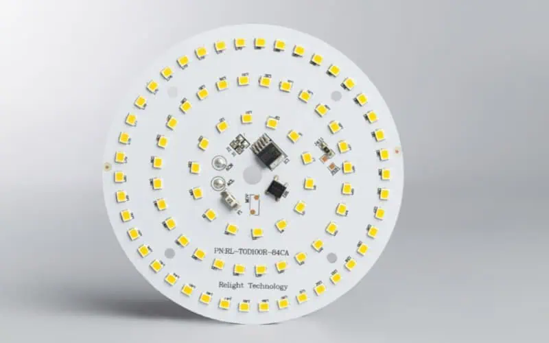
What is an LED PCB?
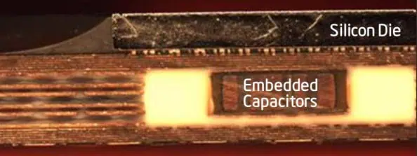
An LED PCB is a specialized circuit board designed to support and power Light Emitting Diodes. These PCBs are engineered to provide optimal electrical, thermal, and mechanical performance for LED applications. They differ from standard PCBs in several ways:
- Enhanced thermal management capabilities
- Specialized copper patterns for current distribution
- Reflective surfaces for improved light output
- Customized layouts for specific LED arrangements
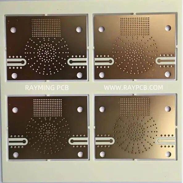
Types of LED PCBs
LED PCBs come in various types, each suited for different applications and performance requirements:
| PCB Type | Description | Advantages | Common Applications |
| FR-4 | Standard fiberglass-based PCB | Cost-effective, widely available | Low-power LED applications |
| Aluminum PCB (MCPCB) | PCB with aluminum base for heat dissipation | Excellent thermal management | High-power LED lighting |
| Ceramic PCB | Made from ceramic materials | Superior thermal performance, high frequency capability | Automotive lighting, high-reliability applications |
| Flexible PCB | Bendable PCB made from flexible materials | Conformable to various s |
Optimization Techniques for LED PCB Design

Thermal Management Strategies
Effective thermal management is crucial for LED PCB performance and longevity. Here are some key strategies:
Heat Dissipation Design
- Thermal vias: Implement an array of thermal vias beneath LED components to efficiently transfer heat from the top layer to the bottom layer or internal heat-spreading planes.
- Copper pour: Maximize copper area on all layers to improve heat spreading and dissipation.
- Thermal pads: Design larger thermal pads for LED components to enhance heat transfer to the PCB.
Material Selection
Choose PCB materials with high thermal conductivity:
| Material | Thermal Conductivity (W/mK) | Advantages |
| FR-4 | 0.25 – 0.5 | Cost-effective, suitable for low-power applications |
| Aluminum PCB | 1.0 – 3.0 | Excellent heat dissipation, ideal for high-power LEDs |
| Ceramic PCB | 20 – 170 | Superior thermal performance, suitable for extr |
Thermal Simulation and Analysis
Utilize thermal simulation software to:
- Identify hotspots on the PCB
- Optimize component placement for better heat distribution
- Validate thermal design before production
Electrical Design Considerations
Current Distribution
- Trace width calculation: Use appropriate trace widths to handle the required current without excessive voltage drop or heat generation.
- Power planes: Implement dedicated power planes for high-current applications to ensure uniform current distribution.
- Star topology: Arrange LED connections in a star topology to maintain consistent voltage across all LEDs.
EMI/EMC Optimization
- Ground plane design: Use a solid ground plane to minimize electromagnetic interference (EMI) and improve signal integrity.
- Component placement: Keep high-frequency components and sensitive signal traces away from power circuits to reduce EMI.
- Filtering: Implement proper filtering techniques, such as decoupling capacitors and ferrite beads, to suppress noise and EMI.
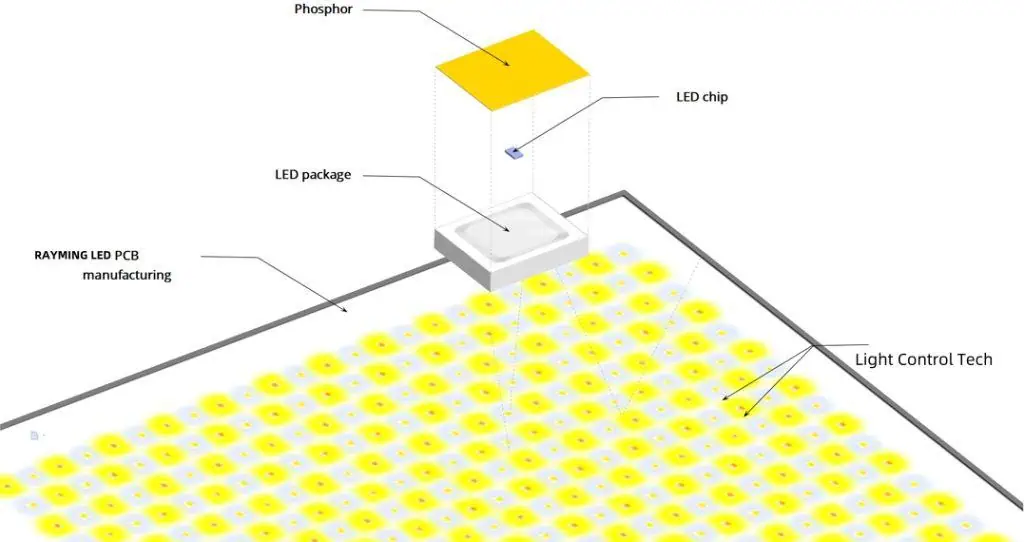
Optical Performance Enhancement
Reflective Surfaces
- White solder mask: Use white solder mask on the LED side of the PCB to increase reflectivity and improve light output.
- Reflective coatings: Apply specialized reflective coatings to enhance light reflection and overall efficiency.
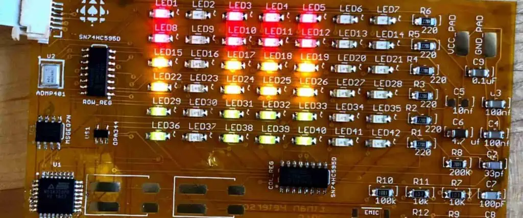
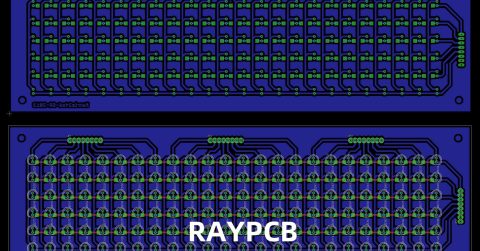
LED Placement and Spacing
- Uniform distribution: Ensure uniform spacing between LEDs to achieve consistent light output and avoid hotspots.
- Angle consideration: Adjust LED placement angles to optimize light distribution for specific applications.
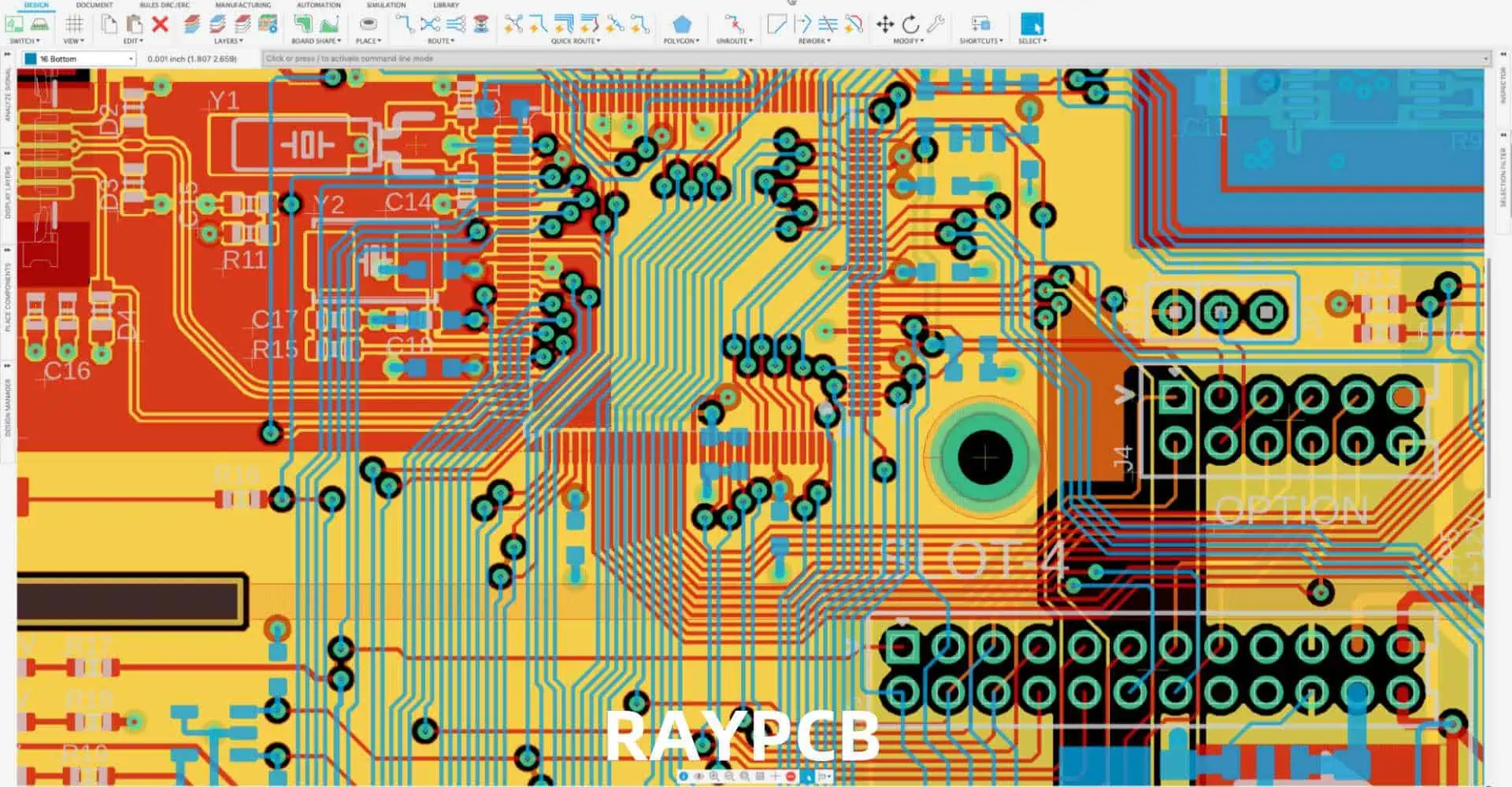
Advanced PCB Design Techniques
Multi-layer PCB Design
Multi-layer PCB designs offer several advantages for complex LED applications:
- Improved thermal management: Dedicated internal layers for heat spreading.
- Enhanced signal integrity: Separation of power and signal layers.
- Increased functionality: More space for additional components and features.
Design considerations for multi-layer LED PCBs:
- Use internal layers for power distribution and heat spreading
- Implement proper layer stackup for optimal performance
- Utilize blind and buried vias for compact designs
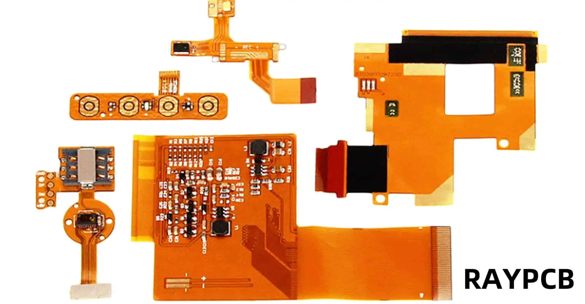
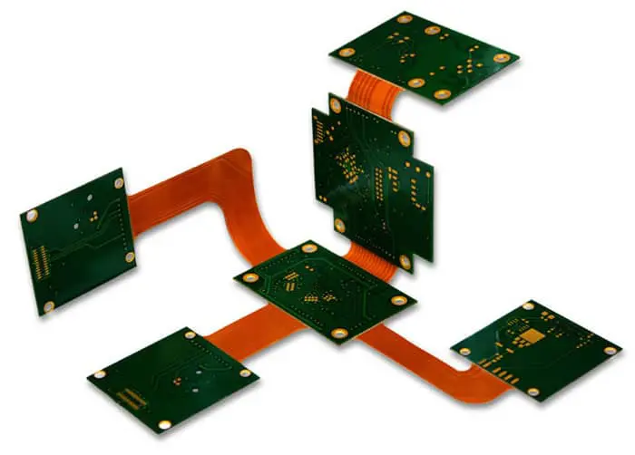
Flexible and Rigid-Flex PCB Design
Flexible and rigid-flex PCBs enable unique LED applications:
- Curved surfaces: Conform to non-planar surfaces for architectural lighting.
- Dynamic lighting: Create movable or foldable LED displays.
- Space-saving designs: Fit LED circuits into compact or irregularly shaped spaces.
Key considerations:
- Choose appropriate flexible materials with good thermal properties
- Design for stress relief in bent areas
- Implement proper layer transitions between rigid and flexible sections
High-Frequency PCB Design for LED Drivers
Modern LED drivers often operate at high frequencies, requiring special PCB design techniques:
- Controlled impedance: Design traces with specific impedance for high-frequency signals.
- Signal integrity: Minimize crosstalk and reflections through proper trace routing and termination.
- EMI suppression: Implement advanced EMI suppression techniques such as guard traces and stitching vias.
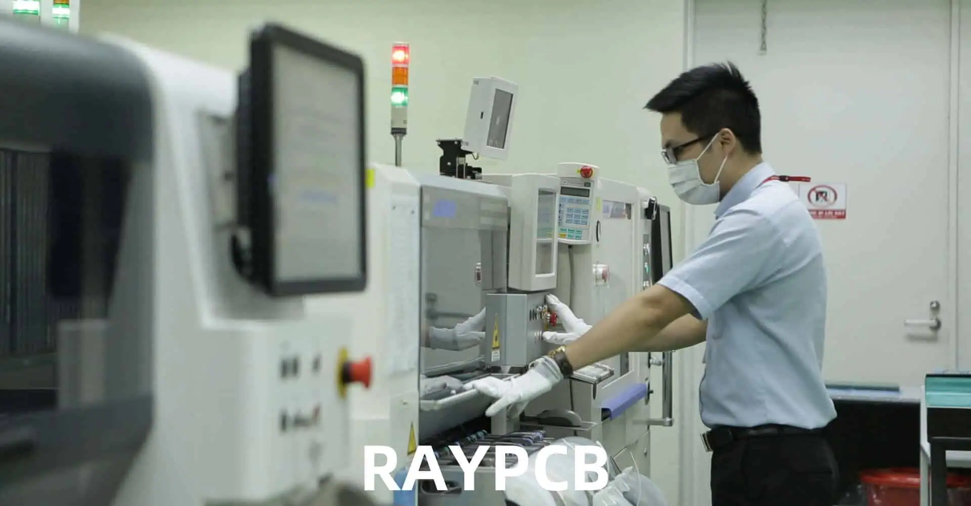
Quality Control Measures for LED PCBs
Incoming Material Inspection
Implement rigorous inspection processes for incoming materials:
- PCB substrate: Check for defects, proper thickness, and material composition.
- Components: Verify authenticity, specifications, and condition of LEDs and other components.
- Solder paste and flux: Ensure proper composition and storage conditions.
In-Process Quality Control
Monitor and control critical parameters during the PCB assembly process:
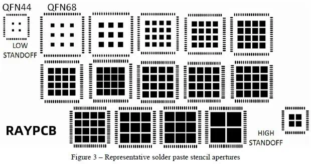
Solder Paste Inspection (SPI)
| Inspection Parameter | Acceptable Range | Potential Issues if Out of Range |
| Paste volume | ±20% of nominal | Insufficient solder joints, tombstoning |
| Paste alignment | ±50% of pad area | Solder bridges, open circuits |
| Paste height | ±25% of stencil thickness | Weak solder joints, component misalignme |
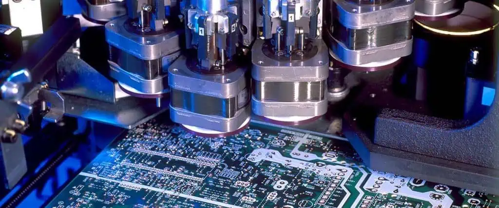
Automated Optical Inspection (AOI)
Implement AOI at various stages of the assembly process:
- Pre-reflow: Verify component placement and orientation.
- Post-reflow: Inspect solder joint quality and component presence.
- Final inspection: Check for overall PCB quality and cleanliness.
X-ray Inspection
Use X-ray inspection for:
- Detecting voids in solder joints, especially for bottom-terminated components.
- Inspecting hidden solder joints in multi-layer or double-sided PCBs.
- Verifying internal layer connections and via structures.
Functional Testing
Develop comprehensive functional test procedures:
- Electrical testing: Verify correct voltages, currents, and LED functionality.
- Thermal testing: Conduct thermal imaging to identify hotspots and verify thermal design.
- Optical testing: Measure light output, color consistency, and beam patterns.
- Environmental testing: Subject PCBs to temperature cycling, humidity, and vibration tests to ensure reliability.
Reliability Testing and Analysis
Implement long-term reliability testing:
- Accelerated life testing: Subject LEDs to elevated temperatures and currents to predict long-term performance.
- Thermal cycling: Expose PCBs to extreme temperature variations to test for thermal stress resistance.
- Failure analysis: Conduct root cause analysis on any failures to improve design and processes.
Emerging Technologies and Future Trends
Advanced Materials
- Graphene-based PCBs: Explore the potential of graphene for improved thermal conductivity and electrical performance.
- Nano-ceramic composites: Investigate new ceramic composites for enhanced thermal management in high-power applications.
Intelligent PCB Design
- AI-assisted design: Utilize artificial intelligence algorithms for optimizing PCB layouts and thermal management.
- Digital twins: Implement digital twin technology for real-time monitoring and predictive maintenance of LED PCBs.
Integration of IoT and Smart Lighting
- Embedded sensors: Integrate environmental and occupancy sensors directly into LED PCBs for smart lighting applications.
- Wireless connectivity: Incorporate low-power wireless modules for IoT-enabled lighting control and monitoring.
Conclusion
Optimizing LED PCB design and quality control is a multifaceted process that requires careful consideration of thermal, electrical, and optical factors. By implementing advanced design techniques, rigorous quality control measures, and staying abreast of emerging technologies, manufacturers can produce high-performance, reliable LED PCBs that meet the demanding requirements of modern lighting applications.
As the LED industry continues to evolve, the integration of new materials, intelligent design processes, and IoT capabilities will further enhance the functionality and efficiency of LED PCBs. Staying informed about these advancements and continuously refining design and quality control processes will be crucial for success in the competitive LED market.
Frequently Asked Questions (FAQ)
- Q: What is the most critical factor in LED PCB design? A: While all aspects are important, thermal management is often considered the most critical factor in LED PCB design. Effective heat dissipation is essential for maintaining LED performance, color stability, and longevity.
- Q: How does the choice of PCB material affect LED performance? A: PCB material significantly impacts thermal management and, consequently, LED performance. Materials with higher thermal conductivity, such as aluminum or ceramic, allow for better heat dissipation, which can lead to improved LED efficiency and lifespan.
- Q: What are the advantages of using multi-layer PCBs for LED applications? A: Multi-layer PCBs offer improved thermal management through dedicated heat-spreading layers, enhanced signal integrity by separating power and signal layers, and increased functionality by providing more space for additional components and features.
- Q: How important is automated inspection in LED PCB quality control? A: Automated inspection, including SPI, AOI, and X-ray inspection, is crucial for maintaining high quality in LED PCB production. These technologies can detect defects that are difficult or impossible to spot with manual inspection, ensuring consistent product quality and reliability.
- Q: What emerging technologies are likely to impact LED PCB design in the near future? A: Key emerging technologies include advanced materials like graphene-based PCBs, AI-assisted design for optimization, digital twin technology for real-time monitoring, and the integration of IoT capabilities for smart lighting applications. These technologies have the potential to significantly enhance LED PCB performance, efficiency, and functionality.