In the world of electronics manufacturing, the reflow soldering process is a critical step in producing high-quality printed circuit board assemblies (PCBAs). The reflow profile, which defines the time-temperature relationship during the soldering process, plays a crucial role in determining the quality of solder joints and the overall reliability of the final product. An incorrectly set up reflow profile can lead to various soldering defects, compromising the integrity and functionality of the PCBA.
This article will explore the various soldering defects that can occur due to an improperly configured reflow profile, their causes, and potential solutions. By understanding these defects and their relationship to the reflow profile, manufacturers can optimize their processes and improve the quality of their PCBAs.
Understanding the Reflow Profile
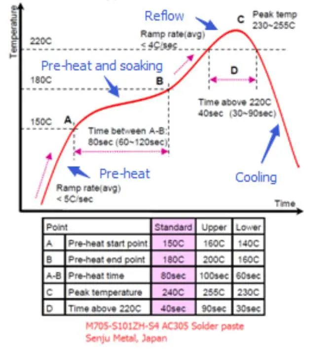
Before delving into specific defects, it’s essential to understand the components of a typical reflow profile and their significance.
Stages of a Reflow Profile
A standard reflow profile consists of four main stages:
- Preheat
- Soak
- Reflow
- Cooling
Each stage serves a specific purpose and contributes to the formation of reliable solder joints.
Key Parameters of a Reflow Profile
The following parameters are critical in defining an appropriate reflow profile:
| Parameter | Description | Typical Range |
| Ramp-up Rate | The rate of temperature increase during preheat | 1-3°C/second |
| Soak Temperature | The temperature maintained during the soak stage | 150-200°C |
| Soak Time | Duration of the soak stage | 60-120 seconds |
| Peak Temperature | Maximum temperature reached during reflow | 230-250°C |
| Time Above Liquidus (TAL) | Time spent above the solder’s melting point | 30-90 seconds |
| Cooling Rate | Rate of temperature decrease after reflow | 2-4°C/second |
Soldering Defects Related to Incorrect Reflow Profiles

Let’s examine the various soldering defects that can occur due to improper reflow profile setup, categorized by the stages of the reflow process.
1. Preheat Stage Defects
1.1 Component Cracking
Cause: Excessively rapid ramp-up rate
Symptoms:
- Visible cracks in component bodies
- Intermittent or complete electrical failure
Solution: Reduce the ramp-up rate to allow for gradual heating of components and PCB
1.2 Tombstoning
Cause: Uneven heating during preheat stage
Symptoms:
- Components standing on one end
- Open circuits
Solution: Ensure uniform heating across the PCB by optimizing oven settings and component placement
2. Soak Stage Defects
2.1 Flux Depletion
Cause: Excessive soak time or temperature
Symptoms:
- Poor wetting
- Dull or grainy solder joints
Solution: Adjust soak time and temperature to allow for proper flux activation without depletion
2.2 Popcorning
Cause: Insufficient soak time for moisture removal
Symptoms:
- Swelling or cracking of plastic components
- Internal delamination
Solution: Increase soak time to allow for gradual moisture removal from components
3. Reflow Stage Defects
3.1 Cold Solder Joints
Cause: Insufficient peak temperature or time above liquidus (TAL)
Symptoms:
- Dull, grainy appearance of solder joints
- Poor electrical connection
Solution: Increase peak temperature and/or extend TAL to ensure complete melting and proper wetting
3.2 Overheating and Component Damage

Cause: Excessive peak temperature or prolonged TAL
Symptoms:
- Discoloration of components
- Charring of PCB
- Component failure
Solution: Reduce peak temperature and/or shorten TAL while ensuring proper solder joint formation
3.3 Solder Balling
Cause: Rapid temperature rise during reflow
Symptoms:
- Small solder balls around solder joints
- Potential short circuits
Solution: Optimize the temperature ramp-up rate during the transition from soak to reflow
3.4 Voiding
Cause: Insufficient time for outgassing during reflow
Symptoms:
- Voids visible in X-ray inspection
- Reduced thermal and electrical conductivity
Solution: Adjust the reflow profile to allow more time for outgassing, potentially including a short plateau just below peak temperature
4. Cooling Stage Defects
4.1 Brittle Solder Joints
Cause: Excessively rapid cooling rate
Symptoms:
- Cracks in solder joints
- Reduced mechanical strength
Solution: Decrease the cooling rate to allow for proper grain structure formation in the solder
4.2 Excessive Intermetallic Growth
Cause: Slow cooling rate or extended time at high temperature
Symptoms:
- Brittle solder joints
- Reduced long-term reliability
Solution: Optimize cooling rate to balance between avoiding thermal shock and minimizing intermetallic growth
Comprehensive Table of Reflow Profile Defects
The following table summarizes the soldering defects related to incorrect reflow profiles, their causes, and solutions:
| Parameter | Description | Typical Range |
| Ramp-up Rate | The rate of temperature increase during preheat | 1-3°C/second |
| Soak Temperature | The temperature maintained during the soak stage | 150-200°C |
| Soak Time | Duration of the soak stage | 60-120 seconds |
| Peak Temperature | Maximum temperature reached during reflow | 230-250°C |
| Time Above Liquidus (TAL) | Time spent above the solder’s melting point | 30-90 seconds |
| Cooling Rate | Rate of temperature decrease after reflow | 2-4°C/second |
Strategies for Optimizing Reflow Profiles
To minimize soldering defects related to reflow profiles, consider the following strategies:
1. Profiling and Monitoring
- Use thermal profiling equipment to measure actual temperatures on the PCB
- Monitor multiple points on the board to ensure uniform heating
- Regularly verify and adjust profiles based on collected data
2. Component-Specific Considerations
- Adjust profiles based on the most sensitive components on the PCB
- Consider using multiple zones or split conveyor ovens for boards with diverse component types
3. Flux and Solder Paste Selection
- Choose solder pastes and fluxes compatible with the intended reflow profile
- Consider low-temperature solders for temperature-sensitive components
4. Oven Maintenance and Calibration
- Regularly calibrate reflow ovens to ensure accuracy
- Perform preventive maintenance to maintain consistent performance
5. Design for Manufacturing (DFM)
- Optimize PCB design and component placement for more uniform heating
- Consider thermal relief patterns for large copper areas
6. Process Control and Documentation
- Implement strict process control measures
- Document and version control reflow profiles for traceability
Impact of Reflow Profile Defects on PCBA Quality
The following table illustrates the potential impact of reflow profile-related defects on overall PCBA quality:
| Quality Aspect | Potential Impact |
| Reliability | Reduced lifespan, increased field failures |
| Functionality | Intermittent or complete circuit failure |
| Yield | Increased defect rates, higher production costs |
| Appearance | Visible defects, customer dissatisfaction |
| Thermal Performance | Poor heat dissipation, component overheating |
| Mechanical Strength | Weak solder joints, susceptibility to mechanical stress |
Conclusion
The reflow profile is a critical factor in achieving high-quality solder joints and reliable PCBAs. By understanding the relationship between reflow profile parameters and potential soldering defects, manufacturers can optimize their processes to minimize defects and improve overall product quality. Regular monitoring, profiling, and adjustment of reflow profiles, combined with attention to component-specific requirements and overall process control, are essential for consistently producing high-quality electronics assemblies.
Frequently Asked Questions (FAQ)
Q1: How often should reflow profiles be checked and adjusted?
A1: Reflow profiles should be checked and potentially adjusted in the following situations:
- When introducing new products or components
- After major maintenance or changes to the reflow oven
- Periodically (e.g., monthly) as part of regular process control
- When experiencing an increase in soldering defects
- When changing solder paste or flux types
Regular monitoring and proactive adjustments help maintain consistent quality and prevent defects.
Q2: Can a single reflow profile work for all types of PCB assemblies?
A2: While it’s possible to use a generalized profile for similar PCB assemblies, it’s not ideal for all types. Factors that may necessitate different profiles include:
- Component mix (e.g., large thermal mass components vs. small surface mount devices)
- PCB thickness and layer count
- Solder paste composition
- Presence of temperature-sensitive components
It’s best to develop and optimize profiles for specific product families or PCB types to ensure optimal results.
Q3: How do lead-free solders affect reflow profile requirements?
A3: Lead-free solders typically require different reflow profiles compared to traditional lead-based solders:
- Higher peak temperatures (typically 230-250°C vs. 210-230°C for lead-based)
- Narrower process windows
- Potentially longer time above liquidus
- More critical cooling rate control
These differences necessitate careful profile optimization to achieve good wetting and minimize defects while avoiding component damage.
Q4: What are the signs that a reflow profile needs adjustment?
A4: Several indicators suggest that a reflow profile may need adjustment:
- Increase in specific defects (e.g., cold joints, tombstoning)
- Changes in solder joint appearance
- Failing quality control tests (e.g., X-ray, ICT, functional testing)
- Component damage or discoloration
- Inconsistent results across different production runs
Regular inspection and testing can help identify these issues early, allowing for timely profile adjustments.
Q5: How does PCB density affect reflow profile requirements?
A5: PCB density can significantly impact reflow profile requirements:
- High-density boards may require slower ramp rates and longer soak times to ensure uniform heating
- Areas with different component densities may heat at different rates, requiring profile compromises or zone-specific adjustments
- Dense boards may benefit from extended TAL to ensure proper wetting of all joints
- Cooling rates may need adjustment to prevent warpage in dense, multi-layer boards
Thermal profiling of actual assemblies is crucial for optimizing profiles for boards with varying densities.