Mixed Signal Layout Considerations

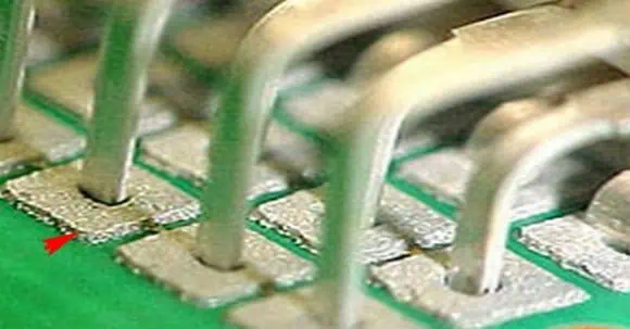
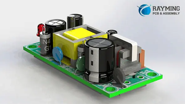
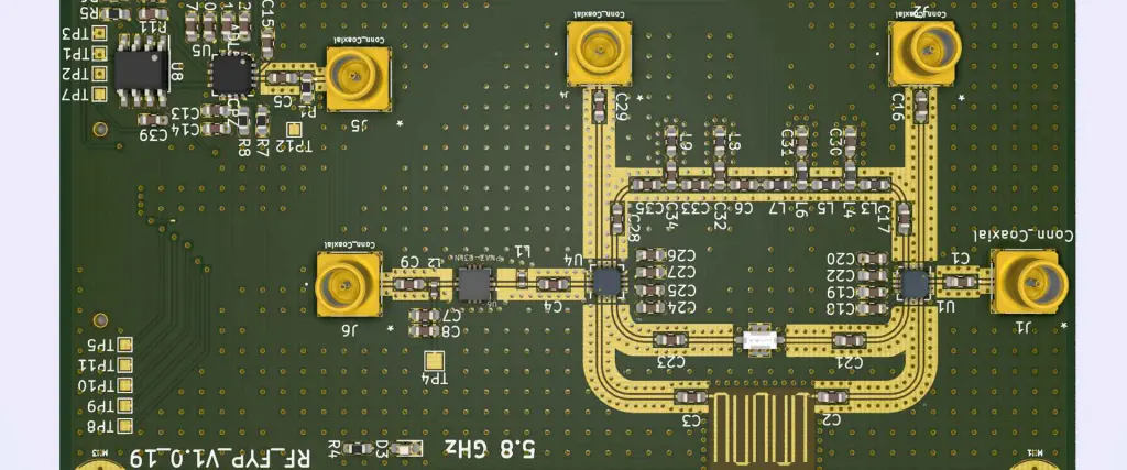
Mixed-signal integrated circuits (ICs) have become increasingly important in modern electronics, combining analog and digital components on a single chip. These ICs present unique challenges in design and layout due to the potential for interference between analog and digital signals. This article explores the key considerations and best practices for mixed-signal layout, aiming to help engineers optimize performance and minimize noise in their designs.

YouTube video

Understanding Mixed-Signal Systems

Definition and Importance

Mixed-signal systems integrate both analog and digital circuitry on a single chip or board. These systems are crucial in various applications, including:

  • Data conversion (ADCs and DACs)
  • Wireless communication devices
  • Sensor interfaces
  • Power management systems

The primary challenge in mixed-signal layout is managing the coexistence of sensitive analog signals with potentially noisy digital signals.

Fundamental Concepts

Before delving into specific layout techniques, it’s essential to understand some fundamental concepts:

Signal Types

signal integrity PCB
Signal TypeCharacteristicsExamples
AnalogContinuous, susceptible to noiseAudio signals, sensor outputs
DigitalDiscrete, more noise-resistantClock signals, data buses
Mixed-SignalCombination of analog and digitalADC inputs, DAC outputs

Noise Sources

  1. Switching noise from digital circuits
  2. Power supply noise
  3. Substrate coupling
  4. Electromagnetic interference (EMI)

Critical Parameters

  • Signal-to-Noise Ratio (SNR)
  • Total Harmonic Distortion (THD)
  • Effective Number of Bits (ENOB) for data converters

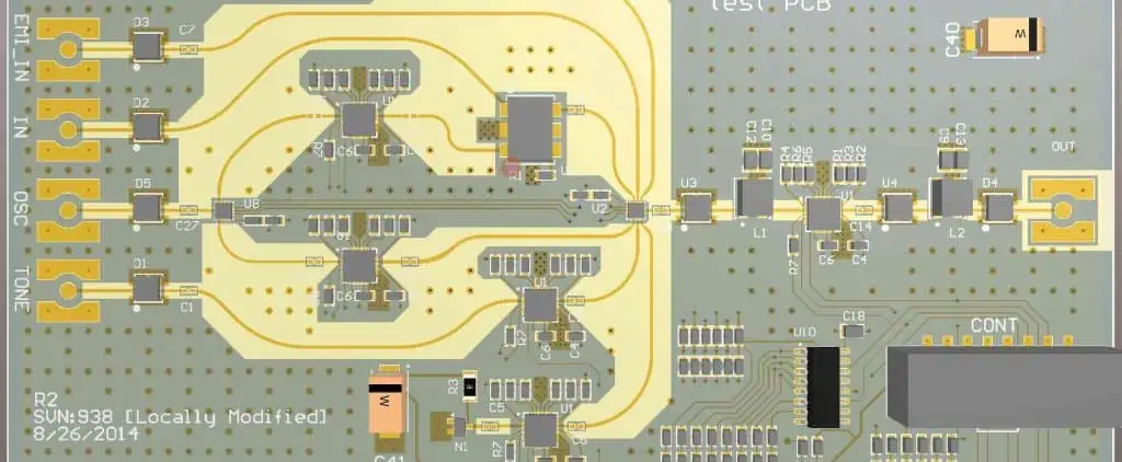
Key Layout Considerations

Partitioning

Importance of Proper Partitioning

Effective partitioning is the foundation of a successful mixed-signal layout. It involves separating analog and digital circuits to minimize interference.

Partitioning Strategies

  1. Physical Separation: Place analog and digital circuits in distinct areas of the chip or board.
  2. Guard Rings: Use guard rings to isolate sensitive analog circuits from digital noise.
  3. Substrate Isolation: Implement deep N-wells or triple-well processes for better isolation.

Power Distribution

Clean Power Supply

Ensuring a clean power supply is crucial for maintaining the integrity of analog signals.

Power Supply Considerations

ConsiderationDescriptionBest Practice
Separate SuppliesUse different power supplies for analog and digital circuitsImplement voltage regulators for each domain
DecouplingAdd decoupling capacitors close to power pinsUse a combination of high and low-value capacitors
Power PlanesDesign separate power planes for analog and digital domainsMinimize overlap between analog and digital planes

Grounding Strategies

Ground Separation

Small signal amplifier

Proper grounding is essential to prevent noise coupling between analog and digital circuits.

Grounding Techniques

  1. Star Grounding: Connect analog and digital grounds at a single point.
  2. Split Ground Planes: Use separate ground planes for analog and digital circuits.
  3. Ground Isolation: Implement moats or cut lines to isolate sensitive analog grounds.
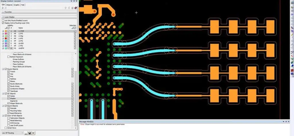
Signal Routing

Critical Signal Paths

Careful routing of critical signals is necessary to maintain signal integrity.

Routing Guidelines

Signal TypeRouting Guideline
AnalogKeep traces short and direct
DigitalUse controlled impedance for high-speed signals
ClockMinimize clock tree skew
Sensitive AnalogShield with ground planes or guard traces

Shielding and Guarding

Electromagnetic Shielding

Shielding helps protect sensitive circuits from external electromagnetic interference.

Shielding Techniques

  1. Metal Layers: Use top metal layers for shielding.
  2. Guard Rings: Implement guard rings around sensitive analog blocks.
  3. EMI Filters: Add EMI filters on board-level designs.

Advanced Layout Techniques

Differential Signaling

Benefits of Differential Signaling

Differential signaling offers improved noise immunity and reduced EMI.

Implementing Differential Signaling

  1. Maintain symmetry in differential pair routing
  2. Use tightly coupled traces for differential pairs
  3. Implement common-mode chokes for additional noise rejection

Substrate Noise Management

Substrate Coupling Mechanisms

Understanding substrate coupling is crucial for minimizing noise in mixed-signal designs.

Substrate Noise Reduction Techniques

  1. Use high-resistivity substrates
  2. Implement guard rings and substrate contacts
  3. Utilize deep N-well isolation for sensitive analog circuits

Clock Distribution

Clock Tree Design

Proper clock distribution is essential for maintaining synchronization and reducing jitter.

Clock Layout Considerations

ConsiderationDescription
Skew MinimizationBalance clock tree branches
Jitter ReductionUse dedicated clock routing layers
EMI ReductionImplement spread spectrum clocking

Thermal Management

Thermal Considerations in Layout

Thermal effects can impact both analog and digital circuit performance.

Thermal Management Techniques

  1. Implement thermal vias for heat dissipation
  2. Use thermal simulations to identify hotspots
  3. Place temperature-sensitive components away from heat sources

Design for Testability and Debugging

RF design
RF design

Test Structures

Importance of Test Structures

Incorporating test structures facilitates easier debugging and characterization.

Common Test Structures

  1. Process control monitors (PCMs)
  2. On-chip ADCs and DACs for signal monitoring
  3. Scan chains for digital circuit testing

Probe Points and Debug Access

Accessibility Considerations

Ensuring accessibility to critical nodes aids in debugging and testing.

Debug Access Implementation

  1. Add probe points for critical analog signals
  2. Implement JTAG interfaces for digital debug
  3. Provide test mode controls for isolating circuit blocks

Layout Verification and Simulation

Design Rule Checking (DRC)

Importance of DRC

DRC ensures that the layout adheres to manufacturing process rules.

Key DRC Checks

  1. Minimum width and spacing rules
  2. Antenna effect checks
  3. Density checks for metal layers

Layout vs. Schematic (LVS)

LVS Verification

LVS ensures that the layout accurately represents the intended circuit.

LVS Considerations

  1. Device matching and symmetry
  2. Parasitic extraction accuracy
  3. Handling of non-standard devices

Post-Layout Simulation

Importance of Post-Layout Simulation

Post-layout simulation accounts for parasitic effects and provides a more accurate performance estimate.

Simulation Considerations

Simulation TypeDescription
Transient AnalysisVerify time-domain performance
AC AnalysisCheck frequency response and stability
Noise AnalysisEvaluate SNR and noise figure
EMI/EMC SimulationAssess electromagnetic compatibility

Industry Best Practices and Standards

Design Guidelines

Common Design Guidelines

  1. Keep analog and digital signals orthogonal when crossing
  2. Use dedicated pins for analog and digital power/ground
  3. Implement guard bands between analog and digital sections

Compliance Standards

Relevant Standards

  1. IEC 61967 (EMI measurements)
  2. JEDEC JEP46 (Guidelines for RF/Analog-Digital Interface)
  3. ISO 26262 (Functional safety for automotive electronics)

Future Trends in Mixed-Signal Layout

Advanced Process Nodes

As process nodes continue to shrink, new challenges and opportunities arise in mixed-signal layout.

Emerging Considerations

  1. Increased impact of quantum effects
  2. Enhanced isolation techniques for 3D IC structures
  3. Integration of RF and mixed-signal in system-on-chip (SoC) designs

AI-Assisted Layout

Artificial intelligence is beginning to play a role in optimizing mixed-signal layouts.

AI Applications in Layout

  1. Automated floorplanning and placement
  2. Machine learning-based parasitic extraction
  3. AI-driven design rule checking and optimization

Frequently Asked Questions (FAQ)

  1. Q: What is the most critical consideration in mixed-signal layout? A: The most critical consideration is proper partitioning and isolation of analog and digital circuits to minimize interference and maintain signal integrity.
  2. Q: How can I reduce substrate noise in my mixed-signal design? A: To reduce substrate noise, you can use techniques such as implementing guard rings, utilizing deep N-well isolation, using high-resistivity substrates, and careful floorplanning to separate noisy digital circuits from sensitive analog components.
  3. Q: What are the advantages of differential signaling in mixed-signal designs? A: Differential signaling offers improved noise immunity, better common-mode rejection, reduced EMI, and can help mitigate the effects of ground bounce and power supply noise.
  4. Q: How important is post-layout simulation in mixed-signal design? A: Post-layout simulation is crucial in mixed-signal design as it accounts for parasitic effects and provides a more accurate representation of the circuit’s performance, helping to identify and address issues that may not be apparent in pre-layout simulations.
  5. Q: What emerging technologies are influencing mixed-signal layout techniques? A: Emerging technologies influencing mixed-signal layout include advanced process nodes with 3D IC structures, the integration of RF components in SoC designs, and the application of artificial intelligence for automated layout optimization and verification.

How to Minimize Negative Effect of ESD on Soldering Joints in SMT Assembly Process

Electrostatic Discharge (ESD) is a significant concern in the electronics manufacturing industry, particularly in Surface Mount Technology (SMT) assembly processes. ESD can cause immediate damage to sensitive electronic components and create latent defects in soldering joints, leading to product failures and reliability issues. This comprehensive guide explores the impact of ESD on soldering joints and provides strategies to minimize its negative effects throughout the SMT assembly process.

YouTube video

Understanding ESD and Its Impact on Soldering Joints

What is ESD?

Electrostatic Discharge (ESD) is the sudden flow of electricity between two electrically charged objects caused by contact, an electrical short, or dielectric breakdown. In electronics manufacturing, ESD typically occurs when a charged person or object comes into contact with a sensitive electronic component or PCB.

ESD Sensitivity Levels

Electronic components have varying levels of sensitivity to ESD. The following table outlines the ESD sensitivity classification according to the Human Body Model (HBM):

ClassVoltage RangeExamples
0< 250VSome MOSFETs, SAW filters
1A250V to <500VVDMOS, ESDs, operational amplifiers
1B500V to <1000VCMOS devices, ECL
1C1000V to <2000VEPROM, JFET, SCR
22000V to <4000VCMOS microcontrollers
3A4000V to <8000VBipolar transistors, 74LS series
3Bโ‰ฅ 8000VPower MOSFETs, power rectifiers

Effects of ESD on Soldering Joints

ESD can negatively impact soldering joints in several ways:

  1. Immediate damage: High-voltage ESD events can cause immediate failure of components or damage to PCB traces.
  2. Latent defects: Lower voltage ESD events may create microscopic damage that leads to premature failure during the product’s lifetime.
  3. Altered material properties: ESD can change the chemical composition or physical structure of solder, flux, or pad surfaces.
  4. Reduced joint reliability: ESD-induced defects can weaken solder joints, making them more susceptible to failure under thermal or mechanical stress.

ESD Control Strategies in SMT Assembly

ESD Protection at pcb soldering

1. Establishing an ESD Protected Area (EPA)

Key Elements of an EPA

  • Grounded work surfaces
  • ESD-safe flooring or mats
  • Ionizers to neutralize static charges
  • Humidity control systems

EPA Certification and Maintenance

  • Regular testing of EPA elements
  • Documenting and addressing non-conformities
  • Training personnel on EPA procedures

2. Personnel ESD Protection

Proper Grounding of Operators

  • Use of wrist straps connected to ground
  • ESD-safe footwear or heel grounders

ESD-Safe Clothing and Personal Items

  • ESD smocks or coveralls
  • Restrictions on personal items in the EPA

Training and Awareness Programs

  • Initial and recurring ESD awareness training
  • Visual reminders and signage in work areas

3. ESD-Safe Equipment and Tools

ESD-Safe Handling Equipment

  • Conductive or dissipative trays and containers
  • ESD-safe tweezers and hand tools

Production Equipment Considerations

  • Proper grounding of all production equipment
  • Use of static dissipative conveyor belts

Maintenance and Verification

  • Regular testing of equipment grounding integrity
  • ESD event detectors on critical equipment

4. Material Management

Component Handling and Storage

  • Use of moisture barrier bags with ESD protection
  • Implementation of ESD-safe component feeders

PCB Handling Procedures

  • Minimize direct handling of PCBs
  • Use of ESD-safe racks and magazines

Solder Paste and Flux Considerations

  • Selection of ESD-safe solder paste containers
  • Proper grounding during solder paste printing

ESD Mitigation in Key SMT Process Steps

How to Do ESD Protection During SMT Assembly

1. PCB Preparation and Handling

Incoming Inspection

  • Use of ESD-safe unpacking areas
  • Implementation of ESD-safe inspection equipment

PCB Storage

  • ESD-safe storage racks or cabinets
  • Proper grounding of PCB magazines

PCB Cleaning (if applicable)

  • Use of ESD-safe cleaning agents
  • Proper grounding of cleaning equipment

2. Solder Paste Printing

Stencil Considerations

  • Use of static dissipative stencil frames
  • Proper grounding of metal stencils

Printer Setup

  • Grounding of squeegees and paste dispensers
  • Use of ionizers near the printing area

Post-Print Handling

  • ESD-safe conveyors for board transport
  • Minimizing manual handling of printed boards

3. Component Placement

Pick and Place Machine Considerations

  • Proper grounding of nozzles and feeders
  • Use of ionizers at component pickup and placement points

Component Feeder Management

  • ESD-safe setup and refilling procedures
  • Regular cleaning and maintenance of feeders

Manual Placement (if applicable)

  • Use of ESD-safe hand tools
  • Proper operator grounding during manual placement

4. Reflow Soldering

Conveyor Systems

  • Use of static dissipative conveyor belts
  • Proper grounding of conveyor frames

Thermal Profile Considerations

  • Awareness of ESD risks during profile measurements
  • ESD-safe thermocouple attachments

Post-Reflow Handling

  • Controlled cooling in an ESD-safe environment
  • ESD-safe board handling after reflow

5. Inspection and Testing

Automated Optical Inspection (AOI)

  • Proper grounding of AOI equipment
  • ESD-safe handling during loading and unloading

X-Ray Inspection

  • ESD protection for sensitive X-ray detectors
  • ESD-safe fixtures for board mounting

In-Circuit Testing (ICT) and Functional Testing

In-Circuit Test (ICT)
  • ESD-safe test fixtures and probes
  • Proper grounding of test equipment

Advanced ESD Mitigation Techniques

1. Ionization Technologies

Types of Ionizers

TypeAdvantagesDisadvantages
CoronaEffective, low maintenanceLimited range, ozone production
NuclearLong-range, no moving partsRegulatory restrictions
Pulsed DCBalanced output, low maintenanceHigher cost
ACWide coverage, cost-effectivePotential for charge accumulation

Strategic Placement of Ionizers

  • Near component feeders
  • Above conveyor systems
  • At manual handling stations

Maintenance and Monitoring

  • Regular cleaning of emitter points
  • Periodic balance and decay time testing

2. ESD Event Detection and Monitoring

Types of ESD Detectors

  • Electromagnetic field (EMF) detectors
  • Surface voltage detectors
  • ESD current sensors

Integration with Production Equipment

  • Real-time monitoring of critical process steps
  • Automated alerts for ESD events

Data Analysis and Trend Monitoring

  • Correlation of ESD events with defect rates
  • Identification of ESD-prone areas or processes

3. Material Innovations

ESD-Safe Solder Pastes

  • Incorporation of static dissipative additives
  • Balanced ESD protection and soldering performance

Advanced PCB Materials

  • Embedded ESD protection layers
  • Static dissipative solder masks

Component Packaging Advancements

  • On-chip ESD protection circuits
  • ESD-safe trays and reels

Implementing an Effective ESD Control Program

1. Risk Assessment

Identifying ESD-Sensitive Areas

  • Process mapping to pinpoint high-risk steps
  • Analysis of component ESD sensitivity levels

Quantifying ESD Risks

  • Use of ESD event detectors to measure occurrence frequency
  • Correlation of ESD events with defect rates

2. Developing ESD Control Procedures

Creating Standard Operating Procedures (SOPs)

  • Detailed instructions for ESD-safe handling
  • Clear guidelines for EPA maintenance

Documentation and Record Keeping

  • ESD control program documentation
  • Logs of ESD events and corrective actions

3. Training and Certification

Initial ESD Awareness Training

  • Basic principles of ESD and its effects
  • Proper use of ESD control equipment

Advanced Training for Key Personnel

  • ESD program management
  • Troubleshooting ESD-related issues

Certification Programs

  • Internal certification processes
  • Industry-recognized certifications (e.g., ESD Association)

4. Continuous Improvement

Regular Audits and Assessments

  • Internal ESD control audits
  • Third-party assessments for objectivity

Performance Metrics and Benchmarking

  • Tracking ESD-related defect rates
  • Benchmarking against industry standards

Feedback Loops and Corrective Actions

  • Prompt investigation of ESD events
  • Implementation and validation of corrective measures

Conclusion

Minimizing the negative effects of ESD on soldering joints in the SMT assembly process requires a comprehensive and proactive approach. By implementing robust ESD control strategies, leveraging advanced mitigation techniques, and fostering a culture of ESD awareness, manufacturers can significantly reduce the risk of ESD-related defects and improve overall product reliability.

Remember that ESD control is an ongoing process that requires constant vigilance and adaptation to new technologies and manufacturing techniques. Regular assessment, training, and improvement of ESD control measures will ensure that your SMT assembly process remains protected against the ever-present threat of electrostatic discharge.

By following the guidelines and strategies outlined in this article, manufacturers can create a more resilient SMT assembly process, resulting in higher quality products, improved customer satisfaction, and reduced costs associated with ESD-related failures.

Frequently Asked Questions (FAQ)

Q1: How can I determine if a soldering defect is caused by ESD?

A1: Identifying ESD as the root cause of a soldering defect can be challenging, as the effects are often not immediately visible. However, some indicators that a defect may be ESD-related include:

  1. Localized damage or discoloration on component leads or pads
  2. Crater-like formations in the solder joint
  3. Thin, whisker-like protrusions from the solder joint
  4. Intermittent failures that cannot be attributed to other causes
  5. Consistent failures of ESD-sensitive components in specific process steps

To confirm ESD as the cause, consider the following steps:

  • Use ESD event detectors to monitor the process and correlate events with defects
  • Perform failure analysis using techniques like cross-sectioning or scanning electron microscopy
  • Temporarily enhance ESD controls in suspected problem areas and observe if defect rates decrease
  • Review handling procedures and ESD control measures for the affected components

Remember that a comprehensive root cause analysis should always be performed, as similar symptoms can sometimes be caused by other factors like contamination or thermal issues.

Q2: What humidity levels are optimal for ESD control in SMT assembly, and how can they be maintained?

A2: Optimal relative humidity (RH) levels for ESD control in SMT assembly typically range from 30% to 70%. Within this range:

  • 40-60% RH is often considered ideal, balancing ESD control with other manufacturing considerations
  • Higher humidity levels (50-60% RH) provide better natural ESD protection but may introduce other issues like moisture sensitivity
  • Lower humidity levels (30-40% RH) may require more aggressive use of ionizers and other ESD control measures

To maintain optimal humidity levels:

  1. Install humidity monitoring systems throughout the production area
  2. Use industrial humidifiers or dehumidifiers as needed
  3. Implement HVAC systems with humidity control capabilities
  4. Create airlocks or transition areas between spaces with different humidity requirements
  5. Consider local humidity control for critical process steps

It’s important to note that while humidity control is beneficial for ESD management, it should not be relied upon as the sole ESD control measure. A comprehensive ESD control program should include grounding, ionization, ESD-safe materials, and proper training regardless of humidity levels.

Q3: How does temperature affect ESD risks in the reflow soldering process, and what precautions should be taken?

A3: Temperature plays a significant role in ESD risks during the reflow soldering process:

  1. Higher temperatures generally reduce ESD risks by:
    • Increasing surface conductivity
    • Reducing triboelectric charging
    • Enhancing charge dissipation
  2. However, the reflow process introduces ESD risks due to:
    • Rapid temperature changes causing pyroelectric charging in some materials
    • Potential for triboelectric charging as boards move through different temperature zones
    • Increased sensitivity of some components at elevated temperatures

Precautions to mitigate ESD risks during reflow soldering:

  • Use properly grounded conveyor systems with static dissipative belts
  • Install ionizers at the entrance and exit of the reflow oven
  • Ensure proper grounding of the reflow oven itself
  • Implement ESD-safe handling procedures for boards entering and exiting the oven
  • Consider nitrogen atmospheres in reflow ovens, which can help reduce ESD risks
  • Monitor ESD events with specialized detectors designed for high-temperature environments
  • Pay special attention to ESD control during profiling and maintenance activities

By implementing these precautions, manufacturers can minimize ESD risks associated with the high temperatures and thermal gradients inherent in the reflow soldering process.

Q4: What are the best practices for handling and storing ESD-sensitive components in an SMT production environment?

A4: Best practices for handling and storing ESD-sensitive components in SMT production include:

  1. Storage:
    • Use ESD-protective packaging (e.g., conductive bags, ESD-safe containers)
    • Implement moisture-barrier bags for moisture-sensitive devices
    • Store components in ESD-protected areas with controlled access
    • Use ESD-safe racks or cabinets for organized storage
  2. Handling:
    • Only handle components in designated ESD Protected Areas (EPAs)
    • Ensure all personnel are properly grounded (wrist straps, ESD footwear)
    • Use ESD-safe tools and equipment for all handling operations
    • Minimize direct contact with component leads or terminals
  3. Transportation:
    • Use ESD-safe carts or trolleys for moving components within the facility
    • Ensure all transport containers are properly labeled for ESD sensitivity
    • Implement ESD-safe practices for receiving and shipping areas
  4. Component Preparation:
    • Perform baking (if required) in ESD-safe ovens
    • Use ESD-safe component straightening tools if needed
    • Conduct any required programming or testing in an EPA
  5. Feeder Loading:
    • Load component feeders in an EPA
    • Use ESD-safe techniques when transferring components to feeders
    • Properly ground all feeders before installation in pick-and-place machines
  6. Inventory Management:
    • Implement first-in-first-out (FIFO) inventory practices
    • Regularly audit storage areas for proper ESD controls
    • Train inventory personnel on proper ESD handling procedures
  7. Documentation and Traceability:
    • Maintain logs of component handling and storage conditions
    • Implement barcode or RFID systems for tracking ESD-sensitive items
    • Regularly review and update handling procedures based on component manufacturer recommendations

By adhering to these best practices, manufacturers can significantly reduce the risk of ESD damage to sensitive components throughout the SMT production process.

Q5: How can we effectively train and motivate personnel to consistently follow ESD control procedures in an SMT assembly environment?

A5: Effective training and motivation of personnel for ESD control in SMT assembly involves a multi-faceted approach:

  1. Comprehensive Training Program:
    • Initial ESD awareness training for all new employees
    • Regular refresher courses (e.g., annually) for all staff
    • Advanced training for ESD coordinators and supervisors
    • Hands-on practical sessions demonstrating proper ESD control techniques
  2. Clear and Accessible Procedures:
    • Develop easy-to-understand Standard Operating Procedures (SOPs) for ESD control
    • Post visual aids and reminders in work areas
    • Provide quick reference guides at workstations
  3. Demonstrate the Impact:
    • Use visual demonstrations of ESD effects (e.g., ESD simulators)
    • Share case studies of ESD-related failures and their costs
    • Conduct “before and after” comparisons showing improved product quality with proper ESD control
  4. Regular Audits and Feedback:
    • Implement a schedule of ESD control audits
    • Provide immediate feedback on compliance and areas for improvement
    • Recognize and reward consistently compliant behavior
  5. Empower Employees:
    • Encourage employees to report ESD control issues or suggest improvements
    • Form ESD control teams with representatives from different departments
    • Involve employees in ESD control equipment selection and procedure development
  6. Use Technology:
    • Implement ESD event detectors with real-time feedback

Elements Influencing SMT Soldering Quality and Improvement Measures

Surface Mount Technology (SMT) soldering is a critical process in modern electronics manufacturing. The quality of SMT soldering directly impacts the reliability, performance, and longevity of electronic devices. As technology advances and components become smaller and more complex, maintaining high soldering quality becomes increasingly challenging. This comprehensive guide explores the various elements that influence SMT soldering quality and presents effective improvement measures to enhance the overall soldering process.

YouTube video

Understanding SMT Soldering

What is SMT Soldering?

Surface Mount Technology (SMT) soldering is a method used to mount electronic components directly onto the surface of printed circuit boards (PCBs). This technique has largely replaced through-hole technology in many applications due to its ability to achieve higher component density, improved performance, and reduced production costs.

Key Advantages of SMT Soldering

AdvantageDescription
MiniaturizationAllows for smaller, more compact electronic devices
Increased component densityMore components can be placed on a single PCB
Improved performanceShorter electrical paths lead to better high-frequency performance
Automated assemblyHighly suitable for automated production processes
Cost-effectivenessReduced material costs and increased production efficiency

Elements Influencing SMT Soldering Quality

1. PCB Design and Quality

PCB Material Selection

The choice of PCB material significantly impacts soldering quality:

  • FR-4 (standard)
  • High-frequency materials (e.g., Rogers, Taconic)
  • Flexible PCB materials

PCB Surface Finish

Different surface finishes affect solderability:

  • HASL (Hot Air Solder Leveling)
  • ENIG (Electroless Nickel Immersion Gold)
  • OSP (Organic Solderability Preservative)
  • Immersion Tin
  • Immersion Silver

Pad Design

Proper pad design is crucial for successful soldering:

  • Pad size and shape
  • Solder mask clearance
  • Via-in-pad design considerations

2. Component Factors

Component Package Types

Various package types present different soldering challenges:

  • Quad Flat Packages (QFP)
  • Ball Grid Arrays (BGA)
  • Chip Scale Packages (CSP)
  • Leadless packages (e.g., QFN, LGA)

Component Quality and Storage

  • Moisture sensitivity levels (MSL)
  • Proper storage and handling
  • Component age and oxidation

Component Placement Accuracy

  • Pick and place machine calibration
  • Component alignment
  • Placement force

3. Solder Paste Characteristics

Solder Alloy Composition

Common solder alloys and their properties:

AlloyCompositionMelting PointApplications
SAC305Sn96.5/Ag3.0/Cu0.5217-220ยฐCGeneral purpose lead-free
SN100CSn/Cu0.7/Ni0.05/Ge0.005227ยฐCLead-free, good fatigue resistance
SnPbSn63/Pb37183ยฐCLegacy leaded solder (restricted use)

Solder Paste Particle Size

  • Type 3 (25-45 ฮผm)
  • Type 4 (20-38 ฮผm)
  • Type 5 (15-25 ฮผm)

Solder Paste Rheology

  • Viscosity
  • Thixotropic properties
  • Slump resistance

4. Stencil Design and Quality

Stencil Thickness

  • Standard thickness (4-6 mil)
  • Step stencils for mixed component types

Aperture Design

  • Area ratio considerations
  • Aspect ratio optimization
  • Custom aperture shapes for specific components

Stencil Material and Manufacturing

  • Stainless steel vs. nickel stencils
  • Laser-cut vs. electroformed stencils
  • Nano-coated stencils for improved release

5. Printing Process Parameters

Printing Speed and Pressure

  • Optimal print speed for different paste types
  • Squeegee pressure adjustment

Squeegee Type and Angle

  • Metal vs. polyurethane squeegees
  • Squeegee angle impact on paste deposit

Snap-off Distance

  • Zero vs. positive snap-off
  • Impact on paste transfer efficiency

6. Reflow Profile Optimization

Reflow Zones and Their Functions

reflow soldering
ZoneFunctionTemperature Range
PreheatActivate flux, gradually heat PCB150-180ยฐC
SoakEqualize temperatures across the board180-210ยฐC
ReflowMelt solder, form jointsAbove liquidus (e.g., 220-250ยฐC for SAC305)
CoolingSolidify solder jointsRamp down to room temperature

Critical Profile Parameters

  • Ramp rate (ยฐC/second)
  • Time above liquidus
  • Peak temperature
  • Cooling rate

Profile Considerations for Different Components

  • Large thermal mass components
  • Temperature-sensitive components
  • Mixed component types on a single PCB

7. Reflow Oven Capabilities

Heating Technologies

  • Convection (forced air)
  • Infrared (IR)
  • Vapor phase

Temperature Control and Uniformity

  • Number of heating zones
  • Temperature sensors and feedback systems
  • Conveyor speed control

Atmosphere Control

  • Nitrogen vs. air atmosphere
  • Oxygen level monitoring

8. Post-Reflow Processes

Cooling Rate Control

  • Natural vs. forced cooling
  • Impact on solder joint microstructure

Cleaning Processes (if applicable)

  • No-clean vs. clean processes
  • Cleaning agent selection
  • Cleaning equipment considerations

Inspection and Quality Control

  • Automated Optical Inspection (AOI)
  • X-ray inspection for hidden joints
  • In-Circuit Testing (ICT)

Improvement Measures for SMT Soldering Quality

1. Design for Manufacturability (DFM)

PCB Layout Optimization

  • Component placement guidelines
  • Thermal relief for large pads
  • Balanced thermal design

Standardization of Pad Designs

  • Create a library of optimized pad designs
  • Ensure consistency across different projects

Collaborative Design Reviews

  • Involve manufacturing engineers in the design process
  • Regular design review meetings with all stakeholders

2. Component Management

Implement Moisture Sensitive Device (MSD) Controls

  • Proper storage in dry cabinets
  • Tracking of floor life
  • Baking procedures when necessary

Incoming Quality Control

  • Sample testing of incoming components
  • X-ray inspection for BGAs and other hidden-joint packages

First Article Inspection

  • Detailed inspection of first production run
  • Verification of component placement and orientation

3. Solder Paste Optimization

Regular Solder Paste Testing

TestPurposeFrequency
ViscosityEnsure consistent printingDaily
Solder ball testCheck reflow performanceWeekly
Print quality inspectionVerify stencil release and definitionEvery shift
Wetting balance testAssess solderabilityMonthly

Proper Solder Paste Handling

  • Temperature-controlled storage
  • Adherence to manufacturer’s recommendations for kneading and usage

Continuous Improvement in Paste Selection

  • Evaluate new solder paste formulations
  • Conduct trials with different particle sizes for fine-pitch applications

4. Stencil Design and Maintenance

Optimize Aperture Design

  • Use area ratio and aspect ratio calculations
  • Implement custom apertures for challenging components

Regular Stencil Cleaning and Inspection

  • Implement automated under-stencil cleaning systems
  • Periodically inspect for wear or damage

Explore Advanced Stencil Technologies

  • Evaluate nano-coated stencils for improved release
  • Consider step stencils for mixed-technology boards

5. Print Process Optimization

Statistical Process Control (SPC) for Printing

  • Implement automated solder paste inspection (SPI)
  • Track key metrics like volume, area, and height of paste deposits

Regular Printer Maintenance and Calibration

  • Develop a preventive maintenance schedule
  • Calibrate critical parameters (e.g., alignment, pressure) regularly

Optimize Printing Parameters

  • Conduct design of experiments (DOE) to find optimal settings
  • Regularly review and update printing parameters

6. Reflow Profile Optimization

Utilize Profiling Software and Equipment

  • Invest in advanced profiling tools
  • Create a library of optimized profiles for different board types

Implement Adaptive Profiling

  • Use real-time monitoring systems
  • Adjust profiles based on actual board temperatures

Conduct Regular Thermal Profiling

  • Profile new board designs
  • Periodically re-profile existing products to account for oven drift

7. Reflow Oven Maintenance and Upgrade

Regular Oven Maintenance

  • Clean and calibrate on a scheduled basis
  • Replace worn components (e.g., conveyor belts, heating elements)

Implement Closed-loop Temperature Control

  • Use multiple thermocouples for accurate temperature mapping
  • Integrate feedback systems for real-time adjustments

Consider Advanced Reflow Technologies

  • Evaluate vapor phase soldering for challenging applications
  • Explore selective soldering for mixed-technology boards

8. Post-Reflow Process Improvements

Optimize Cooling Strategies

  • Implement controlled cooling zones
  • Consider nitrogen cooling for sensitive components

Enhance Inspection Processes

  • Integrate multiple inspection technologies (AOI, AXI, ICT)
  • Develop comprehensive inspection criteria

Implement Effective Failure Analysis

  • Establish a dedicated failure analysis lab
  • Use root cause analysis techniques to address recurring issues

Conclusion

Achieving and maintaining high-quality SMT soldering requires a comprehensive approach that addresses all aspects of the manufacturing process. By understanding the various elements that influence soldering quality and implementing targeted improvement measures, manufacturers can significantly enhance their SMT soldering processes. This, in turn, leads to improved product reliability, reduced defects, and increased customer satisfaction.

Continuous improvement should be at the core of any SMT soldering quality initiative. Regular evaluation of new technologies, materials, and techniques, coupled with ongoing training and development of personnel, will ensure that your SMT soldering processes remain at the cutting edge of industry standards.

Remember that soldering quality is not just about the end result but also about consistency and repeatability. By implementing robust processes, leveraging data-driven decision-making, and fostering a culture of quality throughout the organization, manufacturers can achieve excellence in SMT soldering and maintain a competitive edge in the ever-evolving electronics industry.

Frequently Asked Questions (FAQ)

Q1: What are the most common SMT soldering defects, and how can they be prevented?

A1: Common SMT soldering defects include:

  1. Solder bridges: Excess solder connecting adjacent pads or leads. Prevention: Optimize stencil design, control solder paste volume, and ensure proper component placement.
  2. Insufficient solder: Not enough solder to form a proper joint. Prevention: Adjust stencil aperture design, ensure proper solder paste printing, and optimize reflow profile.
  3. Tombstoning: One end of a component lifts off the pad during reflow. Prevention: Balance pad designs, ensure even heating during reflow, and consider component placement orientation.
  4. Voiding: Voids or air pockets within the solder joint. Prevention: Use low-voiding solder pastes, optimize reflow profile, and consider vacuum reflow for critical applications.
  5. Head-in-pillow: Incomplete wetting between BGA ball and pad. Prevention: Optimize reflow profile, use flux-rich solder pastes, and ensure proper handling of moisture-sensitive devices.

Preventing these defects requires a holistic approach, addressing PCB design, component quality, process parameters, and equipment maintenance.

Q2: How does the transition to lead-free soldering affect SMT quality, and what adjustments are necessary?

A2: The transition to lead-free soldering has several impacts on SMT quality:

  1. Higher melting point: Lead-free alloys typically melt at higher temperatures, requiring adjustments to reflow profiles.
  2. Wetting behavior: Lead-free solders generally have poorer wetting characteristics, which can affect joint formation.
  3. Increased voiding: Some lead-free alloys are more prone to voiding, especially in BGA joints.
  4. Different microstructure: Lead-free joints have a different microstructure, which can affect long-term reliability.

Necessary adjustments include:

  • Updating reflow profiles to accommodate higher temperatures
  • Optimizing pad and stencil designs for lead-free pastes
  • Using more active fluxes to improve wetting
  • Implementing nitrogen reflow to enhance wetting and reduce oxidation
  • Increasing focus on thermal management due to higher process temperatures
  • Enhancing cleaning processes if using higher activity fluxes
  • Updating inspection criteria to account for the different appearance of lead-free joints

Q3: What role does nitrogen atmosphere play in SMT soldering, and when is it beneficial to use?

A3: Nitrogen atmosphere in SMT soldering can provide several benefits:

  1. Improved wetting: Reduces surface tension of molten solder, enhancing wetting.
  2. Reduced oxidation: Prevents oxidation of pad surfaces and solder paste during reflow.
  3. Better thermal transfer: Nitrogen has better heat transfer properties than air.
  4. Improved joint appearance: Often results in shinier, smoother solder joints.
  5. Potential for reduced defects: Can help reduce issues like voiding and non-wetting.

Nitrogen is particularly beneficial in the following situations:

  • When using lead-free solders, which generally have poorer wetting characteristics
  • For fine-pitch or challenging components like BGAs and QFNs
  • In high-reliability applications where joint quality is critical
  • When processing boards with poor solderability or long shelf life
  • For products that require optimal cosmetic appearance of solder joints

However, nitrogen systems add cost and complexity to the reflow process. The decision to use nitrogen should be based on a cost-benefit analysis, considering factors like product requirements, defect rates, and production volume.

Q4: How can manufacturers effectively manage the soldering of boards with mixed component types and thermal masses?

A4: Managing boards with mixed component types and thermal masses requires a multi-faceted approach:

  1. PCB Design:
    • Group components with similar thermal characteristics
    • Use thermal relief pads for large components
    • Consider split planes to manage heat distribution
  2. Stencil Design:
    • Implement step stencils to vary paste volume for different component types
    • Use custom apertures for unique component requirements
  3. Reflow Profile Optimization:
    • Develop a profile that balances the needs of all components
    • Use longer soak times to equalize temperatures across the board
    • Consider ramp-to-spike profiles for boards with extreme mix
  4. Oven Configuration:
    • Use ovens with more heating zones for better profile control
    • Implement bottom-side heating for large thermal mass components
  5. Component Placement:
    • Place large thermal mass components on the same side of the board
    • Avoid placing temperature-sensitive components near high thermal mass ones
  6. Use of Selective Soldering:
    • Consider selective soldering for through-hole components on mixed-technology boards
  7. Thermal Profiling:
    • Use multiple thermocouples to monitor different areas of the board
    • Perform comprehensive profiling for each new board design
  8. Simulation and Modeling:
    • Use thermal simulation software to predict heat distribution
    • Optimize designs based on simulation results

By combining these strategies, manufacturers can achieve consistent soldering quality across all components, regardless of their thermal characteristics.

Q5: What are the key considerations for implementing a robust SMT soldering quality control process?

A5: Implementing a robust SMT soldering quality control process involves several key considerations:

  1. In-Process Monitoring:
    • Implement automated solder paste inspection (SPI) after printing
    • Use in-line AOI (Automated Optical Inspection) after placement and post-reflow
    • Consider real-time process parameter monitoring (e.g., oven temperatures, conveyor speed)
  2. End-of-Line Inspection:
    • Implement final AOI for comprehensive defect detection
    • Use X-ray inspection for hidden joints (e.g., BGAs, bottom-terminated components)
    • Perform In-Circuit Testing (ICT) or Flying Probe Testing for electrical verification
  3. Statistical Process Control (SPC):
    • Track key metrics like defect rates, first-pass yield, and process capability indices
    • Implement control charts to monitor process stability
    • Use trend analysis to identify potential issues before they become critical
  4. Failure Analysis:
    • Establish a dedicated failure analysis lab
    • Implement root cause analysis procedures for defects
    • Use tools like cross-sectioning and scanning electron microscopy for detailed analysis

When to Use PCB Prototype Service and When to Switch to Standard Production Service

In the world of electronics manufacturing, Printed Circuit Boards (PCBs) play a crucial role in bringing innovative ideas to life. The journey from concept to mass production often involves two distinct phases: prototyping and standard production. Understanding when to use PCB prototype assembly services and when to transition to standard production services is essential for optimizing development time, costs, and product quality. This comprehensive guide will explore the nuances of both services, helping you make informed decisions throughout your product development lifecycle.

Understanding PCB Prototype Services

What is PCB Prototyping?

PCB prototyping is the process of creating a small number of PCBs to test and validate a design before committing to large-scale production. This crucial step allows engineers and designers to identify and rectify issues early in the development process.

Key Features of PCB Prototype Services

Feature Description
Quick turnaround Typically 24-72 hours
Low minimum order quantity Often as low as 1-10 boards
Design flexibility Easy to make changes between iterations
Higher per-unit cost Due to low volume and quick production
Limited material options Focus on common materials for quick production
Basic testing Typically includes basic electrical testing

When to Use PCB Prototype Services

1. Early Design Validation

Testing Concept Feasibility

In the initial stages of product development, PCB prototype services are invaluable for testing the feasibility of your design concept. This allows you to:

  • Verify circuit functionality
  • Identify design flaws early
  • Experiment with component placement
  • Test different layout options

Iterative Design Improvements

Prototyping enables rapid design iterations, allowing you to:

  • Fine-tune circuit performance
  • Optimize component placement
  • Improve signal integrity
  • Enhance thermal management

2. Proof of Concept for Stakeholders

Demonstrating Functionality

Prototype PCBs provide tangible evidence of your design’s functionality, which is crucial for:

  • Securing funding from investors
  • Gaining approval from project stakeholders
  • Demonstrating progress to clients or management

User Testing and Feedback

Early prototypes allow you to:

  • Conduct usability tests
  • Gather user feedback
  • Identify potential improvements
  • Validate market demand

3. Pre-production Testing

Compatibility Verification

Before moving to full production, prototypes help verify:

  • Component compatibility
  • Integration with other system elements
  • Compliance with industry standards
  • Electromagnetic interference (EMI) performance

Manufacturing Process Evaluation

Prototyping allows you to:

  • Assess manufacturability
  • Identify potential production challenges
  • Refine assembly processes
  • Optimize for cost-effective manufacturing

Transitioning to Standard Production Services

What is Standard PCB Production?

Standard PCB production refers to the manufacturing of PCBs in larger quantities, typically after the design has been finalized and validated through prototyping.

Key Features of Standard Production Services

Feature Description
Longer lead times Usually 1-3 weeks or more
Higher minimum order quantities Often 100+ boards
Lower per-unit cost Due to economies of scale
Wider range of material options Access to specialty materials
Advanced testing options In-circuit testing, functional testing, etc.
Tighter quality control Stricter tolerances and inspection processes

When to Switch to Standard Production Services

1. Design Finalization

Rogers-RO3035-pcb

Stable Design

Consider switching to standard production when:

  • Multiple prototype iterations have been successful
  • The design has been thoroughly tested and validated
  • No further significant changes are anticipated

Documentation Readiness

Ensure you have:

  • Complete and accurate design files (Gerber files, drill files, etc.)
  • Comprehensive Bill of Materials (BOM)
  • Detailed assembly instructions

2. Increased Demand

Volume Requirements

Transition to standard production when:

  • Order quantities exceed prototype service limits
  • Consistent, ongoing demand is expected
  • Economy of scale benefits outweigh quick-turn costs

Time to Market Considerations

Switch when:

  • Product launch timelines require larger quantities
  • Inventory needs to be built up for anticipated demand
  • Production schedules align with longer lead times

3. Cost Optimization

Per-Unit Cost Reduction

Move to standard production to:

  • Benefit from volume pricing
  • Reduce overall production costs
  • Improve profit margins

Quality-Cost Balance

Consider the transition when:

  • Higher quality standards are required
  • More advanced testing is needed
  • Specialty materials or processes are necessary

4. Manufacturing Process Refinement

Production Line Setup

Switch to standard production to:

  • Establish dedicated production lines
  • Implement automated assembly processes
  • Optimize workflow for high-volume manufacturing

Quality Control Implementation

Transition when you need to:

  • Implement statistical process control
  • Conduct more rigorous testing
  • Establish long-term quality assurance processes

Factors to Consider When Deciding Between Prototype and Standard Production

1. Project Timeline

Factor Prototype Service Standard Production
Urgency Ideal for tight deadlines Better for planned production schedules
Development stage Early to mid-stage Late stage to full production
Time to market Faster for small quantities More efficient for large quantities

2. Budget Constraints

Consideration Prototype Service Standard Production
Upfront costs Lower initial investment Higher setup costs
Per-unit costs Higher for low quantities Lower for high volumes
Total project cost More economical for small runs More cost-effective for large runs

3. Quality Requirements

Aspect Prototype Service Standard Production
Tolerance levels Generally looser Tighter tolerances possible
Consistency May vary between small batches Higher consistency in large runs
Testing depth Basic testing included Advanced testing options available

4. Volume Needs

Requirement Prototype Service Standard Production
Quantity 1-100 boards typically 100+ boards
Scalability Limited Highly scalable
Inventory management Suitable for on-demand production Better for building inventory

5. Design Flexibility

Feature Prototype Service Standard Production
Design changes Easy to implement between runs More costly and time-consuming
Iteration speed Rapid Slower
Customization Highly flexible Less flexible, focused on consistency

Best Practices for Transitioning from Prototype to Standard Production

1. Thorough Design Review

  • Conduct a comprehensive design review before transitioning
  • Involve all relevant stakeholders (engineering, manufacturing, quality assurance)
  • Ensure all design documentation is complete and accurate

2. Pilot Production Run

  • Conduct a small-scale production run as a transition step
  • Use this to validate the manufacturing process
  • Identify and address any scaling issues

3. Supplier Evaluation

  • Assess potential suppliers’ capabilities for high-volume production
  • Consider factors like quality certifications, capacity, and track record
  • Establish clear communication channels and expectations

4. Process Documentation

  • Develop detailed manufacturing process documentation
  • Create comprehensive test plans and quality control procedures
  • Establish clear acceptance criteria for production boards

5. Training and Knowledge Transfer

  • Ensure all team members are familiar with the transition plan
  • Provide training on new processes or equipment if necessary
  • Establish protocols for addressing issues during the transition

Conclusion

The decision to use PCB prototype services or switch to standard production services is a critical one that impacts product development timelines, costs, and quality. By understanding the unique advantages of each service and carefully considering factors such as project timeline, budget constraints, quality requirements, volume needs, and design flexibility, you can make informed decisions that optimize your PCB manufacturing process.

Remember that the transition from prototyping to standard production is not always a one-time event. As products evolve and new versions are developed, you may find yourself cycling between these services. The key is to remain flexible and choose the service that best meets your current needs while keeping an eye on long-term production goals.

By following best practices and maintaining clear communication with your PCB manufacturer, you can ensure a smooth transition from prototype to standard production, ultimately bringing your electronic products to market efficiently and effectively.

Frequently Asked Questions (FAQ)

Q1: How many prototype iterations should I go through before moving to standard production?

A1: The number of prototype iterations can vary greatly depending on the complexity of your design and your specific requirements. However, as a general guideline:

  1. Simple designs: 1-2 iterations
  2. Moderate complexity: 2-3 iterations
  3. Complex or high-performance designs: 3-5 iterations or more

Key indicators that you’re ready to move to standard production include:

  • Consistent performance across multiple prototype runs
  • No critical issues identified in testing
  • Positive feedback from all stakeholders
  • Confidence in the design’s manufacturability at scale

Remember, it’s better to invest in extra prototype iterations than to rush into production with an unrefined design.

Q2: What are the main cost differences between prototype and standard production services?

A2: The cost structure differs significantly between prototype and standard production services:

Cost Factor Prototype Service Standard Production
Setup costs Lower Higher
Per-unit cost Higher Lower
Minimum order value Lower Higher
Design change costs Lower Higher
Testing costs Basic included, advanced costs extra Comprehensive testing options available

Prototype services often have higher per-unit costs due to the low volume and quick turnaround times. However, they offer lower upfront costs and more flexibility for design changes. Standard production has higher setup costs but offers significant per-unit cost savings at higher volumes due to economies of scale.

Q3: How do I ensure my design is ready for standard production?

A3: To ensure your design is ready for standard production:

  1. Conduct thorough testing: Verify functionality, performance, and reliability under various conditions.
  2. Perform a design for manufacturability (DFM) review: Ensure your design adheres to manufacturing guidelines.
  3. Validate component sourcing: Confirm all components are readily available and suitable for volume production.
  4. Review regulatory compliance: Ensure your design meets all relevant industry standards and regulations.
  5. Conduct a pilot production run: Use this to identify any issues that may arise in full-scale production.
  6. Gather stakeholder approval: Ensure all relevant parties (engineering, manufacturing, quality assurance, etc.) sign off on the design.
  7. Prepare comprehensive documentation: Include detailed assembly instructions, test procedures, and quality control processes.
  8. Establish quality metrics: Define clear acceptance criteria for production boards.

By addressing these points, you can minimize the risk of issues arising during the transition to standard production.

Q4: Can I use different manufacturers for prototyping and standard production?

A4: Yes, you can use different manufacturers for prototyping and standard production, and in some cases, it may be advantageous. Here are some considerations:

Pros of using different manufacturers:

  • Specialized expertise: Prototype manufacturers excel at quick-turn, low-volume production, while standard production manufacturers are optimized for high-volume efficiency.
  • Competitive pricing: You can choose the most cost-effective option for each phase.
  • Risk mitigation: Diversifying your supplier base can reduce supply chain risks.

Cons of using different manufacturers:

  • Knowledge transfer: You’ll need to ensure all design details and manufacturing insights are effectively communicated to the production manufacturer.
  • Potential inconsistencies: Different manufacturers may have slightly different processes or capabilities, which could lead to minor variations in the final product.
  • Relationship management: Managing relationships with multiple suppliers can be more time-consuming.

If you decide to use different manufacturers, ensure you have a thorough design transfer process in place and conduct a pilot run with the production manufacturer before full-scale production.

Q5: How do I handle design changes after moving to standard production?

A5: Handling design changes after moving to standard production requires careful management:

  1. Assess the impact: Determine how the change affects functionality, performance, and manufacturability.
  2. Document the change: Create detailed engineering change orders (ECOs) describing the modifications.
  3. Prototype the change: Even in standard production, prototype the change to validate its impact.
  4. Update documentation: Revise all relevant design files, BOMs, and manufacturing instructions.
  5. Communicate with stakeholders: Inform all relevant parties (internal teams, suppliers, customers) about the change.
  6. Manage inventory: Decide how to handle existing inventory and work-in-progress.
  7. Validate production: Conduct a pilot run to ensure the change is successfully implemented in the production process.
  8. Update quality control: Modify testing and inspection procedures as necessary.
  9. Monitor performance: Closely track the first few production runs to ensure the change doesn’t introduce new issues.

Remember, design changes in standard production can be costly and time-consuming, so they should be carefully evaluated and implemented only when necessary. Establishing a formal change management process can help streamline this procedure and minimize disruptions to your production schedule.

Essential Principles of PCB Sourcing

Printed Circuit Boards (PCBs) are the backbone of modern electronics, serving as the foundation for countless devices we use daily. From smartphones to medical equipment, PCBs play a crucial role in ensuring the functionality and reliability of electronic products. As such, sourcing high-quality PCBs is a critical process for manufacturers and engineers alike. This comprehensive guide will delve into the essential principles of PCB sourcing, covering everything from understanding PCB specifications to selecting the right supplier and managing the procurement process.

Understanding PCB Specifications

Types of PCBs

Before diving into the sourcing process, it’s crucial to understand the different types of PCBs available:

  1. Single-sided PCBs
  2. Double-sided PCBs
  3. Multi-layer PCBs
  4. Rigid PCBs
  5. Flexible PCBs
  6. Rigid-flex PCBs

Each type has its own advantages and applications, and selecting the right one depends on factors such as complexity, space constraints, and performance requirements.

Key PCB Parameters

When sourcing PCBs, several key parameters must be considered:

Parameter Description
Board size Dimensions of the PCB
Layer count Number of conductive layers
Material Base material (e.g., FR-4, Rogers, PTFE)
Copper weight Thickness of copper layers
Minimum trace width and spacing Smallest allowable trace width and gap between traces
Hole size Diameter of drilled holes
Surface finish Type of coating on copper pads (e.g., HASL, ENIG, OSP)
Solder mask Color and type of solder mask
Silkscreen Color and content of component markings

Understanding these parameters is crucial for accurately communicating requirements to suppliers and ensuring the received PCBs meet your specifications.

Evaluating PCB Manufacturers

Key Factors in Supplier Selection

Choosing the right PCB manufacturer is critical to the success of your project. Consider the following factors when evaluating potential suppliers:

  1. Manufacturing capabilities
  2. Quality certifications
  3. Experience and expertise
  4. Production capacity
  5. Turnaround time
  6. Customer support
  7. Price and cost structure
  8. Geographic location
  9. Environmental compliance
  10. Intellectual property protection

Assessing Manufacturing Capabilities

To ensure a supplier can meet your specific requirements, evaluate their manufacturing capabilities:

Capability Description
Minimum trace width and spacing Smallest features the manufacturer can reliably produce
Maximum layer count Highest number of layers the manufacturer can produce
Board size limits Minimum and maximum board dimensions
Via technology Types of vias supported (e.g., through-hole, blind, buried)
Special materials Ability to work with high-frequency or high-temperature materials
Advanced processes Capabilities like impedance control, backdrilling, or sequential lamination

Quality Certifications and Standards

Look for manufacturers with relevant certifications:

  • ISO 9001: Quality management systems
  • IPC-A-600: Acceptability of printed boards
  • AS9100: Quality management for aerospace industry
  • IATF 16949: Quality management for automotive industry
  • ISO 13485: Quality management for medical devices
  • UL Certification: Safety standards compliance

The PCB Sourcing Process

Step 1: Define Requirements

Clearly outline your PCB requirements, including:

  • Electrical specifications
  • Mechanical specifications
  • Environmental requirements
  • Regulatory compliance needs
  • Production volume
  • Delivery timeline

Step 2: Request for Quotation (RFQ)

Prepare a detailed RFQ document including:

  • PCB specifications
  • Design files (Gerber files, drill files, etc.)
  • Bill of Materials (BOM)
  • Quality requirements
  • Delivery requirements
  • Packaging specifications

Step 3: Vendor Selection

Evaluate received quotes based on:

  • Price
  • Lead time
  • Quality assurance
  • Technical capabilities
  • Previous experience
  • Customer reviews and references

Step 4: Prototype and Testing

Before moving to full production:

  1. Order a small batch of prototype PCBs ASSEMBLY
  2. Conduct thorough testing and evaluation
  3. Provide feedback to the manufacturer
  4. Make necessary adjustments to the design or manufacturing process

Step 5: Production and Quality Control

Once satisfied with prototypes:

  1. Place the full production order
  2. Establish quality control checkpoints
  3. Request regular progress updates
  4. Conduct incoming quality inspection upon receipt

Cost Considerations in PCB Sourcing

Factors Affecting PCB Cost

Understanding the factors that influence PCB cost can help in negotiating better prices and making informed decisions:

Factor Impact on Cost
Board size Larger boards generally cost more
Layer count More layers increase complexity and cost
Material Specialty materials are more expensive than standard FR-4
Copper weight Heavier copper increases material cost
Minimum trace width and spacing Tighter tolerances require more advanced manufacturing processes
Hole density More holes increase drilling time and cost
Surface finish Some finishes (e.g., ENIG) are more expensive than others (e.g., HASL)
Solder mask Special colors or types may incur additional costs
Production volume Higher volumes typically result in lower per-unit costs
Turnaround time Expedited orders often come with premium pricing

Cost Reduction Strategies

To optimize PCB sourcing costs:

  1. Design for manufacturability (DFM)
  2. Standardize board sizes and specifications where possible
  3. Consider panel utilization to minimize waste
  4. Evaluate different surface finish options
  5. Optimize layer count and stack-up
  6. Consolidate orders for higher volume discounts
  7. Plan ahead to avoid rush fees
  8. Consider offshore manufacturing for high-volume, non-critical components

Managing PCB Supply Chain Risks

Common Supply Chain Risks

Identifying and mitigating supply chain risks is crucial for maintaining a steady supply of PCBs:

  1. Single-source dependency
  2. Quality inconsistencies
  3. Intellectual property theft
  4. Counterfeit components
  5. Geopolitical instability
  6. Natural disasters
  7. Capacity constraints
  8. Regulatory changes
  9. Currency fluctuations
  10. Obsolescence

Risk Mitigation Strategies

Implement the following strategies to minimize supply chain risks:

  1. Dual sourcing: Qualify multiple suppliers for critical components
  2. Buffer inventory: Maintain safety stock for essential PCBs
  3. Supplier audits: Regularly assess supplier performance and capabilities
  4. Contractual protections: Include quality, delivery, and IP protection clauses in contracts
  5. Supply chain visibility: Implement systems to track orders and inventory in real-time
  6. Contingency planning: Develop backup plans for potential disruptions
  7. Supplier relationship management: Foster strong partnerships with key suppliers
  8. Demand forecasting: Improve accuracy of demand predictions to optimize inventory levels
  9. Design for multiple sources: Create designs that can be manufactured by different suppliers
  10. Regular market analysis: Stay informed about industry trends and potential risks

Emerging Trends in PCB Sourcing

Stay ahead of the curve by considering these emerging trends:

  1. Digital transformation: Online platforms for quoting, ordering, and tracking PCBs
  2. Artificial Intelligence: AI-powered design for manufacturability (DFM) checks
  3. Additive manufacturing: 3D-printed electronics for rapid prototyping
  4. Sustainable materials: Eco-friendly PCB materials and manufacturing processes
  5. Internet of Things (IoT): Increased demand for flexible and high-frequency PCBs
  6. 5G technology: Growing need for high-speed, low-loss PCB materials
  7. Miniaturization: Continued push for smaller, denser PCB designs
  8. Automation: Increased use of robotics in PCB manufacturing
  9. Blockchain: Enhanced traceability and counterfeit prevention
  10. Virtual and augmented reality: Improved design visualization and collaboration tools

Conclusion

Effective PCB sourcing is a critical component of successful electronic product development and manufacturing. By understanding PCB specifications, carefully evaluating suppliers, implementing a structured sourcing process, and staying informed about industry trends, organizations can optimize their PCB procurement strategy. This not only ensures a steady supply of high-quality PCBs but also contributes to overall product quality, time-to-market, and cost-effectiveness.

Remember that PCB sourcing is an ongoing process that requires continuous evaluation and improvement. Stay engaged with your suppliers, keep abreast of technological advancements, and be prepared to adapt your sourcing strategy as market conditions and product requirements evolve.

Frequently Asked Questions (FAQ)

Q1: How do I choose between domestic and offshore PCB manufacturers?

A1: The decision between domestic and offshore PCB manufacturers depends on several factors:

  • Cost: Offshore manufacturers often offer lower prices, especially for high-volume orders.
  • Lead time: Domestic manufacturers typically provide faster turnaround times.
  • Quality: Both can offer high quality, but domestic suppliers may have stricter quality control.
  • Communication: Language barriers and time zone differences can complicate offshore relationships.
  • Intellectual property protection: Domestic suppliers may offer stronger IP protection.

Consider your specific needs in terms of cost, quality, lead time, and IP protection to make the best decision for your project.

Q2: What are the most important quality control measures for PCB sourcing?

A2: Key quality control measures for PCB sourcing include:

  1. Design for manufacturability (DFM) checks
  2. First article inspection
  3. In-process quality control
  4. Electrical testing (e.g., flying probe, bed of nails)
  5. Visual inspection
  6. X-ray inspection for multi-layer boards
  7. Solderability testing
  8. Cleanliness testing
  9. Thermal stress testing
  10. Dimensional verification

Implement a combination of these measures to ensure consistent PCB quality.

Q3: How can I reduce PCB sourcing lead times?

A3: To reduce PCB sourcing lead times:

  1. Optimize your design for manufacturability
  2. Use standard materials and processes where possible
  3. Provide complete and accurate design files
  4. Consider quick-turn PCB services for prototypes
  5. Develop relationships with reliable suppliers
  6. Plan ahead and forecast demand accurately
  7. Use panel designs to maximize production efficiency
  8. Consider local manufacturers for urgent needs
  9. Implement a vendor-managed inventory system
  10. Use online ordering platforms for faster quoting and ordering

Q4: What are the key considerations when sourcing flex and rigid-flex PCBs?

A4: When sourcing flex and rigid-flex PCBs, consider:

  1. Material selection (e.g., polyimide, FR-4)
  2. Bend radius and flexibility requirements
  3. Layer stack-up design
  4. Copper weight and distribution
  5. Surface finish compatibility with flexing
  6. Adhesiveless construction for improved reliability
  7. Coverlay vs. solder mask for flex areas
  8. Strain relief design
  9. Manufacturer’s experience with flex and rigid-flex
  10. Testing and qualification processes specific to flex circuits

Q5: How do I ensure my PCB supplier can meet my long-term needs?

A5: To ensure your PCB supplier can meet your long-term needs:

  1. Assess their financial stability and business outlook
  2. Evaluate their technology roadmap and investment in new equipment
  3. Check their capacity and ability to scale production
  4. Review their quality management systems and continuous improvement processes
  5. Discuss long-term partnership opportunities and volume pricing
  6. Assess their supply chain resilience and risk management strategies
  7. Consider their ability to adapt to changing regulations and environmental standards
  8. Evaluate their commitment to innovation and new technology adoption
  9. Review their track record of meeting long-term customer needs
  10. Establish clear communication channels and regular performance reviews

By considering these factors, you can select a PCB supplier that will be a reliable partner for your current and future projects.

Design of High-Power PCB in High Temperature Environment

In the realm of electronic design, high-power printed circuit boards (PCBs) operating in high-temperature environments present a unique set of challenges. These specialized PCBs are crucial in various industries, including automotive, aerospace, industrial automation, and power electronics. This article delves into the intricacies of designing high-power PCBs capable of withstanding and performing optimally in elevated temperature conditions.

YouTube video

Understanding High-Power PCBs

Definition and Applications

High-power PCBs are designed to handle significant electrical currents and dissipate large amounts of heat. They find applications in:

  1. Power supplies
  2. Motor controllers
  3. LED lighting systems
  4. Renewable energy systems
  5. Electric vehicle components

Challenges in High-Temperature Environments

Operating in high-temperature environments exacerbates the challenges faced by high-power PCBs:

  1. Increased thermal stress
  2. Accelerated component degradation
  3. Reduced electrical performance
  4. Material limitations
  5. Reliability concerns

Key Considerations in High-Power PCB Design

Thermal Management

Effective thermal management is paramount in high-power PCB design, especially in high-temperature environments.

Heat Dissipation Techniques

  1. Copper Pour: Maximizing copper coverage for better heat distribution
  2. Thermal Vias: Facilitating heat transfer between layers
  3. Heat Sinks: External components for enhanced cooling
  4. Active Cooling: Fans or liquid cooling systems for extreme cases

Thermal Simulation and Analysis

Utilizing thermal simulation software to:

  1. Identify hotspots
  2. Optimize component placement
  3. Validate cooling solutions

Material Selection

Choosing appropriate materials is crucial for high-temperature operation.

PCB Substrate Materials

MaterialMax Operating Temp (ยฐC)Thermal Conductivity (W/mK)Relative Cost
FR-41300.3Low
Polyimide2600.3Medium
Aluminum150150-170High
Ceramic>30020-270Very High

Solder Mask and Surface Finish

Select high-temperature resistant options:

  1. High-Temp Solder Mask: Withstands temperatures up to 280ยฐC
  2. ENIG (Electroless Nickel Immersion Gold): Suitable for high-temp applications

Component Selection and Placement

High-Temperature Components

Choose components rated for high-temperature operation:

  1. Ceramic capacitors with high voltage ratings
  2. High-temp resistors (e.g., metal film, wirewound)
  3. Semiconductors with extended temperature ranges

Component Placement Strategy

  1. Group high-heat components
  2. Maintain adequate spacing for thermal relief
  3. Consider airflow patterns in forced-air cooling designs

Power Distribution and Copper Weight

Copper Thickness

Increase copper weight for better current handling and heat dissipation:

Copper Weight (oz)Thickness (ฮผm)Current Capacity
135Standard
270Increased
3105High
4140Very High

Power Planes and Trace Design

  1. Use wide traces for high-current paths
  2. Implement split power planes for different voltage domains
  3. Consider using buried or embedded power planes

Impedance Control and Signal Integrity

High temperatures can affect signal integrity. Implement:

  1. Controlled impedance routing
  2. Proper stackup design
  3. Signal isolation techniques

Reliability and Longevity Considerations

Thermal Cycling and Expansion

Address thermal expansion mismatches:

  1. Use materials with matched Coefficient of Thermal Expansion (CTE)
  2. Implement stress-relief design techniques

Conformal Coating

Apply conformal coating to protect against:

  1. Moisture
  2. Dust
  3. Chemical contaminants

Advanced Design Techniques

Switching Power Supply Design

Multi-Layer PCB Design

Leverage multi-layer designs for improved thermal management and signal integrity:

  1. Dedicate layers for power distribution
  2. Use internal layers for signal routing
  3. Implement ground planes for better EMI shielding

Embedded Components

Consider embedding passive components:

  1. Reduces board size
  2. Improves thermal performance
  3. Enhances reliability in high-vibration environments

3D Design Considerations

Utilize 3D design techniques for:

  1. Optimizing component placement
  2. Integrating cooling solutions
  3. Improving overall board density

Manufacturing Considerations

PCB Fabrication

Select a fabricator experienced in high-power, high-temperature PCBs:

  1. Capability to handle thick copper
  2. Expertise in high-temp materials
  3. Advanced drilling and plating processes

Assembly Challenges

Address assembly challenges specific to high-temp designs:

  1. Use high-temperature solder alloys
  2. Implement special handling procedures for sensitive components
  3. Consider vapor phase soldering for uniform heating

Testing and Validation

Thermal Testing

Conduct comprehensive thermal testing:

  1. Temperature cycling tests
  2. Thermal imaging analysis
  3. Power cycling tests

Electrical Testing

Perform electrical tests under high-temperature conditions:

  1. Functional testing at elevated temperatures
  2. Accelerated life testing
  3. EMI/EMC testing in high-temp environments

Case Studies

Case Study 1: Automotive Power Module

Challenge: Design a power module for electric vehicle inverters operating in temperatures up to 150ยฐC.

Solution:

  1. Used aluminum nitride ceramic substrate
  2. Implemented direct bonded copper (DBC) for improved thermal management
  3. Utilized high-temp SiC MOSFETs
  4. Integrated liquid cooling system

Outcome: Achieved reliable operation at 150ยฐC with 30% improvement in power density.

Case Study 2: Industrial Motor Controller

Challenge: Develop a motor controller PCB for high-temperature industrial environments (up to 100ยฐC ambient).

Solution:

  1. Selected polyimide substrate
  2. Implemented thick copper (3 oz) power planes
  3. Used conformal coating for environmental protection
  4. Designed custom heatsink with forced-air cooling

Outcome: Successful operation in 100ยฐC ambient with 50% reduction in thermal-related failures.

Future Trends

Advanced Materials

Research into new materials for extreme environments:

  1. High-temperature polymers
  2. Ceramic-based composites
  3. Graphene-enhanced substrates

Wide Bandgap Semiconductors

Increasing adoption of wide bandgap semiconductors:

  1. Gallium Nitride (GaN)
  2. Silicon Carbide (SiC)

Integrated Cooling Solutions

Development of more efficient cooling techniques:

  1. Microfluidic cooling channels
  2. Phase-change materials
  3. Thermoelectric cooling integration

Conclusion

High Power board
High Power board

Designing high-power PCBs for high-temperature environments requires a multifaceted approach, combining material science, thermal management, electrical engineering, and manufacturing expertise. By carefully considering all aspects of the design process, from material selection to advanced cooling techniques, engineers can create robust and reliable PCBs capable of operating in the most demanding conditions.

As technology advances, new materials, components, and design techniques will continue to push the boundaries of what’s possible in high-power, high-temperature PCB design. Staying abreast of these developments and continuously refining design practices will be crucial for meeting the ever-increasing demands of industries relying on these specialized PCBs.

FAQ

Q1: What is considered a “high temperature” for PCB operation?

A1: In PCB design, “high temperature” typically refers to operating environments above 85ยฐC. However, the exact definition can vary depending on the industry and application. For consumer electronics, temperatures above 70ยฐC might be considered high, while in automotive or industrial applications, high temperature could mean operating at 125ยฐC or even higher. For extreme applications, such as in oil and gas exploration or aerospace, high temperature could exceed 200ยฐC.

Q2: How does high temperature affect the choice of PCB substrate material?

A2: High temperatures significantly impact the choice of PCB substrate material. Standard FR-4 materials typically have a maximum operating temperature of around 130ยฐC. For higher temperatures, more specialized materials are required:

  1. High-Tg FR-4: Suitable for temperatures up to 170ยฐC
  2. Polyimide: Can withstand temperatures up to 260ยฐC
  3. Ceramic substrates: Capable of operating at temperatures exceeding 300ยฐC

The choice depends not only on the maximum temperature but also on factors like thermal cycling, coefficient of thermal expansion (CTE), and cost considerations.

Q3: What are some key strategies for improving heat dissipation in high-power PCBs?

A3: Several strategies can be employed to improve heat dissipation in high-power PCBs:

  1. Increasing copper weight and using copper pours
  2. Implementing thermal vias to conduct heat between layers
  3. Using metal-core or insulated metal substrate (IMS) PCBs
  4. Integrating heat sinks or heat spreaders
  5. Designing for effective air or liquid cooling
  6. Optimizing component placement for better heat distribution
  7. Utilizing advanced thermal management materials like gap fillers or phase-change materials

The most effective approach often involves a combination of these strategies, tailored to the specific requirements of the design.

Q4: How do high temperatures affect the reliability and lifespan of PCB components?

A4: High temperatures can significantly impact the reliability and lifespan of PCB components:

  1. Accelerated aging: Heat accelerates chemical reactions that cause component degradation.
  2. Thermal stress: Repeated heating and cooling can lead to mechanical stress and eventual failure.
  3. Decreased performance: Many components show reduced efficiency or altered characteristics at high temperatures.
  4. Increased leakage currents: Higher temperatures can increase leakage in semiconductors.
  5. Reduced capacitor lifespan: Electrolytic capacitors, in particular, can dry out faster at high temperatures.

To mitigate these effects, designers must choose components rated for high-temperature operation, implement effective cooling solutions, and consider derating components to ensure they operate well within their specified limits.

Q5: What are the challenges in testing high-power PCBs designed for high-temperature environments?

A5: Testing high-power PCBs for high-temperature environments presents several challenges:

  1. Simulating realistic operating conditions: Creating test setups that accurately replicate the intended operating environment can be complex and expensive.
  2. Safety concerns: High-power, high-temperature testing can pose safety risks and require specialized equipment and procedures.
  3. Accelerated life testing: Predicting long-term reliability through accelerated testing requires careful planning and interpretation.
  4. Thermal cycling effects: Testing must account for the stresses induced by thermal cycling, not just steady-state high temperatures.
  5. Component interactions: High temperatures can affect component interactions in ways that might not be apparent in room-temperature testing.
  6. Equipment limitations: Standard test equipment may not be suitable for high-temperature operation, requiring specialized high-temp test gear.

Overcoming these challenges often requires a combination of sophisticated thermal chambers, custom test fixtures, specialized measurement equipment, and carefully designed test protocols.

PCB Material Selection Based on Electrical Performance and Cost in Communication Network Field

Printed Circuit Boards (PCBs) are the backbone of modern electronic devices, particularly in the communication network field. The selection of appropriate PCB materials is crucial for achieving optimal electrical performance while managing costs effectively. This article delves into the intricacies of PCB material selection, focusing on the balance between electrical performance and cost considerations in the context of communication networks.

YouTube video

Understanding PCB Materials

Basic PCB Structure

Before diving into material selection, it’s essential to understand the basic structure of a PCB:

  1. Substrate: The base material that provides mechanical support
  2. Copper Foil: Conductive layers for electrical connections
  3. Solder Mask: Protective layer to prevent short circuits
  4. Silkscreen: Printed labels and markings

Common PCB Materials

Substrate Materials

Copper-Clad-Board-Material

The substrate forms the foundation of the PCB and significantly influences its electrical and mechanical properties. Common substrate materials include:

  1. FR-4 (Flame Retardant 4)
  2. Rogers Materials
  3. Polyimide
  4. PTFE (Polytetrafluoroethylene)
  5. Ceramic

Copper Foil

Copper is the primary conductor used in PCBs due to its excellent electrical conductivity and cost-effectiveness.

Electrical Performance Considerations

Dielectric Constant (Dk)

The dielectric constant, also known as relative permittivity, is a crucial factor in determining the electrical performance of a PCB material. It affects signal propagation speed and impedance control.

Dissipation Factor (Df)

The dissipation factor, or loss tangent, measures the amount of energy lost as signals travel through the PCB material. Lower Df values indicate better performance, especially at high frequencies.

Coefficient of Thermal Expansion (CTE)

CTE is important for maintaining the structural integrity of the PCB across varying temperatures, which is crucial for reliable electrical performance.

Thermal Conductivity

Effective heat dissipation is essential for maintaining stable electrical performance, especially in high-power applications.

Cost Considerations

Material Costs

The raw material cost is a significant factor in PCB production. Here’s a comparison of relative costs for common PCB materials:

MaterialRelative Cost
FR-4Low
RogersHigh
PolyimideMedium-High
PTFEHigh
CeramicVery High

Processing Costs

Different materials require varying levels of processing complexity, which affects overall production costs:

MaterialProcessing ComplexityRelative Processing Cost
FR-4LowLow
RogersMediumMedium-High
PolyimideMediumMedium
PTFEHighHigh
CeramicVery HighVery High

Volume Considerations

The production volume significantly impacts the overall cost per unit. High-volume production can offset the initial high material costs for premium substrates.

Material Selection for Communication Networks

Low-Frequency Applications

For low-frequency applications (below 1 GHz), cost-effective materials like FR-4 are often sufficient:

PropertyFR-4 (Typical Values)
Dk4.2-4.8
Df0.014-0.020
CTE (ppm/ยฐC)50-70 in X,Y; 200-250 in Z
CostLow

High-Frequency Applications

For high-frequency applications (above 1 GHz), advanced materials like Rogers or PTFE-based substrates are preferred:

PropertyRogers RO4350BPTFE-based
Dk3.482.1-2.5
Df0.00370.0006-0.0020
CTE (ppm/ยฐC)10-12 in X,Y20-25 in X,Y
CostHighVery High

5G and Beyond

For cutting-edge communication networks like 5G and future technologies, even more specialized materials may be required:

PropertyRogers RO3003Ceramic
Dk39.8-10.2
Df0.0010.0001-0.0005
CTE (ppm/ยฐC)17 in X,Y5.5-7.1
CostVery HighExtremely High

Balancing Performance and Cost

Hybrid Designs

To optimize both performance and cost, many PCB designers opt for hybrid designs:

  1. Use high-performance materials only for critical high-frequency sections
  2. Employ standard FR-4 for low-frequency or non-critical areas
  3. Implement multi-layer designs with mixed materials

Material Selection Strategy

  1. Identify the frequency range and critical performance parameters for the application
  2. Determine the production volume and budget constraints
  3. Consider environmental factors (temperature, humidity, etc.)
  4. Evaluate available materials based on electrical properties and cost
  5. Prototype and test with different material combinations
  6. Optimize the design based on test results and cost analysis

Case Studies

Case Study 1: 4G LTE Base Station PCB

Requirements:

  • Frequency range: 700 MHz to 2.6 GHz
  • High reliability and thermal stability
  • Cost-sensitive due to large-scale deployment

Solution:

  • Hybrid design using Rogers RO4350B for critical RF sections
  • FR-4 for low-frequency and digital sections
  • 8-layer stackup with mixed materials

Outcome:

  • Achieved required RF performance
  • 30% cost reduction compared to full Rogers design
  • Improved thermal management due to optimized material selection

Case Study 2: 5G mmWave Small Cell PCB

Requirements:

  • Frequency range: 24 GHz to 40 GHz
  • Extremely low loss
  • Compact design

Solution:

  • Rogers RO3003 for antenna and critical mmWave sections
  • PTFE-based material for feed networks
  • Ceramic substrate for filters

Outcome:

  • Met stringent RF performance requirements
  • Achieved miniaturization goals
  • Higher cost justified by performance in critical 5G infrastructure

Future Trends in PCB Materials for Communication Networks

Fr4 Laminate
Fr4 Laminate

Advanced Composites

Research is ongoing into new composite materials that combine the benefits of different substrates:

  • Ceramic-filled PTFE for improved thermal management
  • Nanomaterial-enhanced epoxies for better electrical performance

Eco-Friendly Materials

As environmental concerns grow, the industry is moving towards more sustainable PCB materials:

  • Halogen-free substrates
  • Biodegradable PCB materials
  • Recyclable conductive materials

Smart Materials

The future may see the integration of smart materials in PCBs:

  • Self-healing conductors
  • Adaptive dielectrics that change properties based on environmental conditions

Conclusion

Selecting the right PCB material for communication network applications requires a careful balance of electrical performance and cost considerations. As technology advances, the demand for high-performance, cost-effective PCB materials continues to grow. By understanding the properties of various materials and employing strategic design approaches, engineers can create optimal solutions that meet both technical requirements and budgetary constraints.

The future of PCB materials in the communication network field looks promising, with ongoing research into advanced composites, eco-friendly options, and smart materials. As these innovations come to fruition, they will undoubtedly reshape the landscape of PCB design and manufacturing, enabling even more powerful and efficient communication networks.

FAQ

Q1: What is the most important electrical property to consider when selecting PCB materials for high-frequency applications?

A1: For high-frequency applications, the most critical electrical property is typically the dissipation factor (Df) or loss tangent. A lower Df value indicates less signal loss, which is crucial for maintaining signal integrity at high frequencies. However, the dielectric constant (Dk) is also very important for impedance control and signal propagation speed.

Q2: Can I use FR-4 for all my PCB designs to keep costs low?

A2: While FR-4 is a cost-effective and versatile material suitable for many applications, it may not be appropriate for all designs, especially those involving high frequencies (generally above 1 GHz) or requiring very low loss. For high-frequency or high-performance applications, more advanced materials like Rogers or PTFE-based substrates may be necessary to meet electrical performance requirements.

Q3: How does the choice of PCB material affect the manufacturing process?

A3: Different PCB materials have varying processing requirements. For example, PTFE-based materials often require special handling and processing techniques due to their soft nature and high melting point. Ceramic substrates may need specialized cutting and drilling processes. These factors can affect manufacturing time, complexity, and cost. Standard materials like FR-4 are generally easier and cheaper to process.

Q4: Are there any environmental considerations when selecting PCB materials?

A4: Yes, environmental factors are becoming increasingly important in PCB material selection. Some considerations include:

  • Halogen-free materials to reduce environmental impact
  • RoHS (Restriction of Hazardous Substances) compliance
  • Recyclability and end-of-life disposal
  • Energy efficiency in the manufacturing process

Q5: How do I determine if a hybrid material approach is suitable for my PCB design?

A5: A hybrid material approach may be suitable if your PCB design has distinct sections with different performance requirements. Consider a hybrid approach if:

  1. Your design has both high-frequency and low-frequency sections
  2. Only specific areas require high-performance materials
  3. You need to balance cost and performance
  4. There are significant differences in thermal management requirements across the board

Evaluate the performance requirements of each section of your PCB and consider using high-performance materials only where necessary to optimize both cost and performance.

Panel Requirements for Assembly during SMT

Surface Mount Technology (SMT) has revolutionized the electronics manufacturing industry, enabling the production of smaller, more complex, and highly efficient printed circuit boards (PCBs). A critical aspect of the SMT process is the use of panelized PCBs, which allows for more efficient handling and prototype assembly of multiple boards simultaneously. This article delves into the essential panel requirements for assembly during SMT, exploring the various factors that influence panel design, manufacturing, and processing.

Understanding Panelization in SMT

What is Panelization?

Panelization is the process of combining multiple individual PCBs into a single, larger panel for more efficient production. This approach offers several advantages in SMT assembly:

  1. Improved handling and automation
  2. Increased production efficiency
  3. Better use of manufacturing equipment
  4. Enhanced quality control
  5. Reduced material waste

Types of Panels

There are several types of panels used in SMT assembly:

  1. Array panels: Multiple identical PCBs arranged in a grid
  2. Mixed panels: Different PCB designs combined on a single panel
  3. Multiblock panels: Large PCBs segmented into smaller blocks for assembly
  4. Single PCB panels: Individual PCBs with added borders for handling

Key Panel Requirements for SMT Assembly

SONY DSC

1. Panel Size and Thickness

The dimensions and thickness of the panel are crucial for compatibility with SMT equipment and processes.

Factors influencing panel size:

  • SMT equipment specifications
  • Pick-and-place machine capabilities
  • Reflow oven dimensions
  • Handling and storage considerations

Standard panel sizes:

Panel Type Dimensions (inches) Typical Applications
Full 18 x 24 High-volume production
Half 18 x 12 Medium-volume production
Quarter 12 x 9 Low-volume or prototype runs
Custom Varies Specific product requirements

Panel thickness considerations:

  • Typical range: 0.031″ to 0.093″ (0.8mm to 2.4mm)
  • Thicker panels may require special handling equipment
  • Thinner panels may need additional support to prevent warping

2. Panel Material and Construction

The choice of panel material affects both the manufacturing process and the final product quality.

Common panel materials:

  1. FR-4 (Flame Retardant 4)
  2. High-Tg FR-4
  3. Polyimide
  4. Ceramic
  5. Metal-core PCBs

Material selection factors:

  • Thermal properties
  • Electrical requirements
  • Mechanical strength
  • Cost considerations

3. Fiducial Marks

Fiducial marks are essential for accurate component placement during SMT assembly.

Types of fiducials:

  1. Global fiducials (panel-level)
  2. Local fiducials (board-level)
  3. Tooling fiducials

Fiducial design guidelines:

  • Minimum size: 1mm diameter
  • Clearance around fiducial: 2-3mm
  • Contrasting color to the PCB surface
  • Typically copper with solder mask clearance

4. Tooling Holes and Edges

Proper tooling features ensure accurate alignment and secure handling during the SMT process.

Tooling hole requirements:

  • Diameter: Typically 3mm to 4mm
  • Location: At least three holes, ideally at corners
  • Edge clearance: Minimum 5mm from panel edge

Edge considerations:

  • Smooth edges to prevent snagging
  • Rounded corners to reduce stress concentration
  • Clearance from components and traces

5. Break-out Methods

The method used to separate individual PCBs from the panel affects both manufacturing efficiency and board quality.

Common break-out methods:

  1. V-scoring
  2. Perforated tabs
  3. Route and retain
  4. Pinned breakaway

Comparison of break-out methods:

Method Advantages Disadvantages
V-scoring Clean break, fast separation Limited to straight lines, potential for damage
Perforated tabs Flexible design, easy manual separation Requires finishing, potential for uneven edges
Route and retain Smooth edges, complex shapes possible More expensive, slower process
Pinned breakaway Strong panel integrity, good for odd shapes Requires manual separation, potent

6. Component Clearance and Spacing

Proper spacing between components and panel edges is crucial for successful SMT assembly.

Key clearance considerations:

  • Edge clearance: Minimum 5mm from panel edge to components
  • Inter-board spacing: Typically 2-3mm between individual PCBs
  • Component height restrictions based on SMT equipment

7. Solder Paste Stencil Compatibility

The panel design must accommodate the use of solder paste stencils for efficient and accurate paste deposition.

Stencil design factors:

  • Stencil thickness: Typically 4-8 mils (0.1-0.2mm)
  • Aperture design for different component types
  • Consideration of step stencils for mixed component heights

8. Thermal Management

Panel design must account for thermal considerations during the reflow soldering process.

Thermal design factors:

  • Even heat distribution across the panel
  • Consideration of thermal mass differences
  • Use of thermal relief patterns for large copper areas

9. Electrical Test Points

Incorporating test points in the panel design facilitates efficient electrical testing post-assembly.

Test point guidelines:

  • Minimum size: 1mm x 1mm
  • Clearance around test points: 0.5mm
  • Consistent placement for automated testing

10. Panel Markings and Labeling

Clear and comprehensive markings on the panel aid in traceability and assembly guidance.

Essential panel markings:

  • Part numbers and revisions
  • Date codes
  • Polarity indicators
  • Assembly instructions or reference designators

Advanced Panel Design Considerations

1. Mixed Technology Panels

Panels that combine SMT and through-hole technology require special considerations.

Design factors:

  • Separate SMT and through-hole sections
  • Consideration of different soldering processes
  • Potential use of selective soldering techniques

2. Flexible and Rigid-Flex Panels

Flexible and rigid-flex PCBs present unique panelization challenges.

Special requirements:

  • Use of support frames or carriers
  • Consideration of bend radii and stress points
  • Special handling procedures during assembly

3. High-Density Interconnect (HDI) Panels

HDI boards often require more precise panelization techniques.

HDI panel considerations:

  • Tighter tolerances for fiducials and tooling holes
  • Special break-out methods to protect fine features
  • Enhanced cleanliness requirements

4. Panels for Automated Optical Inspection (AOI)

Panel design should facilitate efficient AOI processes.

AOI-friendly design features:

  • Fiducials for camera alignment
  • Consistent component orientation
  • Adequate contrast for defect detection

Panel Design Best Practices for SMT Assembly

1. Collaborative Design Approach

Involving SMT assembly experts early in the panel design process can prevent issues and optimize production.

Key collaboration points:

  • PCB designer
  • SMT process engineer
  • Manufacturing engineer
  • Quality assurance team

2. Design for Manufacturing (DFM) Guidelines

Adhering to DFM principles ensures smoother SMT assembly processes.

DFM considerations for panelization:

  • Standardization of panel sizes when possible
  • Consideration of equipment limitations
  • Optimization for pick-and-place efficiency

3. Simulation and Prototyping

Using simulation tools and creating prototypes can identify potential issues before full production.

Simulation aspects:

  • Thermal simulation for reflow process
  • Mechanical stress analysis for break-out methods
  • Assembly process simulation

4. Documentation and Specification

Comprehensive documentation of panel requirements ensures consistent manufacturing and assembly.

Essential documentation:

  • Detailed panel drawings
  • Material specifications
  • Assembly and break-out instructions
  • Test requirements

Emerging Trends in Panel Design for SMT

1. Automation and Industry 4.0

Increasing automation in SMT assembly is driving changes in panel design.

Automation-friendly features:

  • Enhanced traceability through RFID or barcodes
  • Design for robotic handling and assembly
  • Integration with Manufacturing Execution Systems (MES)

2. Sustainable Panel Design

Growing focus on sustainability is influencing panel design choices.

Eco-friendly considerations:

  • Use of recyclable materials
  • Design for disassembly and recycling
  • Optimization to reduce material waste

3. Advanced Materials

New PCB materials are expanding possibilities in panel design.

Emerging materials:

How to Panelize in AlTIum Designer
  • High-frequency laminates for 5G applications
  • Thermally conductive substrates
  • Biodegradable PCB materials

4. Miniaturization and High-Density Assembly

Continued trend towards smaller, denser electronics impacts panel requirements.

Challenges in high-density panels:

  • Finer pitch components and traces
  • Increased importance of planarity control
  • Enhanced thermal management requirements

Conclusion

Effective panel design is crucial for successful SMT assembly, impacting everything from production efficiency to final product quality. By understanding and implementing the key panel requirements outlined in this article, electronics manufacturers can optimize their SMT processes, reduce costs, and improve product reliability.

As the electronics industry continues to evolve, panel design for SMT assembly will face new challenges and opportunities. Staying informed about emerging trends, materials, and technologies will be essential for maintaining competitive advantage in this dynamic field. By embracing best practices in panel design and remaining adaptable to new developments, manufacturers can ensure they are well-positioned to meet the demands of future electronics production.

Frequently Asked Questions (FAQ)

1. What are the most common panel sizes used in SMT assembly?

The most common panel sizes used in SMT assembly are:

  1. Full panel: 18″ x 24″ (457mm x 610mm)
  2. Half panel: 18″ x 12″ (457mm x 305mm)
  3. Quarter panel: 12″ x 9″ (305mm x 229mm)

However, the exact sizes can vary depending on the manufacturer’s equipment and specific product requirements. Many companies also use custom panel sizes optimized for their particular needs.

2. How does panel thickness affect the SMT assembly process?

Panel thickness can significantly impact the SMT assembly process in several ways:

  1. Handling: Thicker panels are generally more robust and easier to handle, but may require specialized equipment.
  2. Warpage: Thinner panels are more prone to warpage during reflow soldering, which can affect component placement accuracy.
  3. Thermal properties: Thicker panels have greater thermal mass, which can affect reflow profiles and soldering quality.
  4. Component compatibility: Some components may have restrictions on maximum board thickness.

Typical panel thicknesses range from 0.031″ to 0.093″ (0.8mm to 2.4mm), with the choice depending on the specific application and assembly requirements.

3. What are the advantages and disadvantages of V-scoring versus routed break-out methods?

V-scoring and routing are two common methods for panel break-out. Here’s a comparison:

V-scoring: Advantages:

  • Fast and cost-effective for straight-line separations
  • Clean break with minimal post-processing required
  • Suitable for high-volume production

Disadvantages:

  • Limited to straight lines only
  • Risk of damaging nearby components or traces
  • Potential for inconsistent breaks in thicker boards

Routing: Advantages:

  • Allows for complex board shapes and curved edges
  • Provides smoother edges with no additional finishing required
  • Reduces stress on the PCB during separation

Disadvantages:

  • More expensive and time-consuming process
  • Requires more space between boards for the router path
  • May generate more dust and debris during separation

The choice between these methods depends on factors such as board design, production volume, and quality requirements.

4. How do fiducial marks improve SMT assembly accuracy?

Fiducial marks play a crucial role in improving SMT assembly accuracy by:

  1. Providing reference points for the pick-and-place machine’s vision system to align the board precisely.
  2. Compensating for minor variations in panel position or orientation during the assembly process.
  3. Allowing for correction of thermal expansion or contraction of the panel.
  4. Enabling more accurate component placement, especially for fine-pitch or BGA components.

There are typically two types of fiducials:

  • Global fiducials: Used to align the entire panel
  • Local fiducials: Used for precise alignment of individual boards or critical components

Properly designed and placed fiducials can significantly reduce assembly defects and improve overall product quality.

5. What are the key considerations for designing panels for mixed-technology boards (combining SMT and through-hole components)?

Designing panels for mixed-technology boards requires careful consideration of several factors:

  1. Component placement: Separate SMT and through-hole component areas to optimize for different assembly processes.
  2. Panel orientation: Ensure the panel can be processed in both SMT and wave soldering equipment if required.
  3. Break-out method: Choose a method that protects both SMT and through-hole components during separation.
  4. Thermal management: Consider the different thermal requirements for SMT reflow and wave soldering processes.
  5. Selective soldering: Plan for potential use of selective soldering techniques for through-hole components.
  6. Tooling holes: Ensure compatibility with both SMT and through-hole assembly equipment.
  7. Test access: Design for both in-circuit testing (ICT) and functional testing requirements.
  8. Assembly sequence: Plan the optimal order of SMT and through-hole assembly steps.

By carefully addressing these considerations, manufacturers can create efficient panel designs that accommodate both SMT and through-hole technologies, maximizing production efficiency and product quality.

PCB Design for Radio Frequency Circuit and Electromagnetic Compatibility

In the rapidly evolving world of electronics, radio frequency (RF) circuits play a crucial role in wireless communication systems, radar technology, and numerous other applications. Designing printed circuit boards (PCBs) for RF circuits presents unique challenges, particularly in ensuring electromagnetic compatibility (EMC). This article delves into the intricacies of PCB design for RF circuits, focusing on key principles, best practices, and strategies to achieve optimal performance while maintaining electromagnetic compatibility.

YouTube video

Understanding RF Circuits and Electromagnetic Compatibility

What are RF Circuits?

Radio Frequency circuits operate in the frequency range from about 3 kHz to 300 GHz. These circuits are essential in various applications, including:

  1. Wireless communication devices
  2. Radar systems
  3. Satellite communications
  4. Broadcasting equipment
  5. Medical imaging devices

The Importance of Electromagnetic Compatibility

Electromagnetic Compatibility (EMC) refers to the ability of electronic equipment to function correctly in its intended electromagnetic environment without introducing intolerable electromagnetic disturbances to other equipment. In RF circuit design, EMC is crucial for:

  1. Ensuring proper functionality of the circuit
  2. Complying with regulatory standards
  3. Minimizing interference with other devices
  4. Enhancing overall system reliability

Key Considerations in RF PCB Design

1. Substrate Selection

The choice of PCB substrate is critical in RF design due to its impact on signal propagation and loss.

Factors to consider:

Comparison of common RF PCB substrates:

Substrate MaterialDielectric Constant (ฮตr)Loss Tangent (tan  ฮด)Thermal StabilityRelative Cost
FR-44.2-4.80.02ModerateLow
Rogers RO4350B3.480.0037ExcellentModerate
Taconic RF-353.50.0018GoodModerate
PTFE (Teflon)2.10.0002ExcellentHigh

2. Impedance Matching and Control

Maintaining consistent impedance throughout the RF signal path is crucial for minimizing reflections and maximizing power transfer.

Key aspects:

  • Transmission line width calculation
  • Use of impedance calculators
  • Consideration of manufacturing tolerances

3. Transmission Line Design

Proper transmission line design is essential for efficient signal propagation in RF circuits.

Common transmission line types:

  1. Microstrip
  2. Stripline
  3. Coplanar waveguide (CPW)

Factors affecting transmission line performance:

  • Line width and spacing
  • Substrate thickness
  • Dielectric constant
  • Ground plane proximity

4. Ground Plane Design

A well-designed ground plane is crucial for RF performance and EMC.

Best practices:

  • Use of solid ground planes
  • Minimizing splits or gaps
  • Proper via stitching
  • Consideration of return current paths

5. Component Placement and Routing

Strategic placement and routing of components are vital for RF circuit performance.

Guidelines:

  • Keep RF traces short and direct
  • Use symmetrical layouts for differential pairs
  • Avoid right-angle bends in RF traces
  • Maintain adequate spacing between RF and digital sections

6. Shielding and Isolation

Effective shielding and isolation techniques help minimize electromagnetic interference (EMI) and crosstalk.

Techniques:

  • Use of EMI shields
  • Implementation of guard traces
  • Proper partitioning of RF and digital sections
  • Use of via fencing

Advanced RF PCB Design Techniques

RF PCB

1. Multi-Layer RF PCB Design

Multi-layer PCBs offer additional flexibility and performance benefits for complex RF designs.

Advantages:

  • Improved isolation between circuits
  • More efficient use of board space
  • Enhanced power distribution
  • Better control of impedance and crosstalk

Design considerations:

  • Layer stack-up optimization
  • Proper use of buried and blind vias
  • Careful management of interlayer transitions

2. High-Speed Digital Interfaces in RF Designs

Many modern RF systems incorporate high-speed digital interfaces, requiring special design considerations.

Key points:

  • Proper termination of high-speed lines
  • Controlled impedance routing
  • Minimizing crosstalk between digital and RF sections
  • Use of appropriate decoupling techniques

3. Thermal Management in RF PCBs

Effective thermal management is crucial for the reliability and performance of RF circuits.

Strategies:

  • Use of thermal vias
  • Implementation of copper coins or heat sinks
  • Proper component placement for heat dissipation
  • Consideration of thermal simulation tools

4. Design for Manufacturability and Testability

Ensuring that RF PCBs are manufacturable and testable is essential for successful production.

Considerations:

  • Adherence to manufacturing design rules
  • Inclusion of test points and probe access
  • Consideration of automated assembly requirements
  • Documentation of critical RF parameters and tolerances

EMC Considerations in RF PCB Design

1. EMI Reduction Techniques

Minimizing electromagnetic interference is crucial for both circuit performance and regulatory compliance.

Strategies:

  • Proper grounding and shielding
  • Use of EMI suppression components
  • Filtering of power supplies
  • Careful routing to minimize EMI coupling

2. EMC Testing and Compliance

Understanding and designing for EMC compliance is essential in RF PCB development.

Key aspects:

  • Familiarity with relevant EMC standards (e.g., FCC, CE)
  • Design for pre-compliance testing
  • Consideration of EMC test setups in PCB design
  • Documentation of EMC design choices and rationale

3. Radiated Emissions Control

Controlling radiated emissions is a critical aspect of EMC in RF PCB design.

Techniques:

  • Minimizing loop areas in current paths
  • Proper termination of unused traces
  • Use of spread spectrum techniques where applicable
  • Implementation of EMI gaskets and conductive coatings

4. Susceptibility and Immunity Considerations

Ensuring that RF circuits are resistant to external electromagnetic interference is crucial for reliable operation.

Design strategies:

  • Proper filtering of input/output lines
  • Use of differential signaling where appropriate
  • Implementation of guard bands around sensitive circuits
  • Consideration of board-level shielding techniques

Tools and Software for RF PCB Design

1. Electromagnetic Simulation Tools

EM simulation tools are invaluable for predicting and optimizing RF PCB performance.

Popular tools:

  • Ansys HFSS
  • CST Microwave Studio
  • Keysight ADS
  • Sonnet Software

2. PCB Design Software with RF Capabilities

Specialized PCB design software with RF features can greatly aid in the design process.

Key features to look for:

  • Impedance-controlled routing
  • RF-specific component libraries
  • Integration with EM simulation tools
  • Advanced stackup management

3. Signal Integrity and Power Integrity Analysis Tools

SI/PI tools help ensure proper signal transmission and power distribution in RF designs.

Important capabilities:

  • Time-domain reflectometry (TDR) simulation
  • S-parameter analysis
  • Power distribution network (PDN) analysis
  • Crosstalk prediction and mitigation

Best Practices for RF PCB Design and EMC

1. Design Planning and Documentation

Thorough planning and documentation are crucial for successful RF PCB design.

Key elements:

  • Detailed specification of RF performance requirements
  • Documentation of EMC considerations and strategies
  • Clear definition of critical RF paths and components
  • Maintenance of design revision history

2. Prototyping and Iterative Design

Embracing an iterative design approach with prototyping can lead to optimized RF PCB performance.

Best practices:

  • Use of evaluation boards for critical components
  • Implementation of modular design for easy modification
  • Planned iterations for performance optimization
  • Thorough testing at each design stage

3. Collaboration between RF, Digital, and PCB Designers

Effective collaboration among different design disciplines is essential for complex RF PCBs.

Strategies for success:

  • Regular design reviews and cross-functional meetings
  • Clear communication of design constraints and requirements
  • Use of collaborative design tools and platforms
  • Shared understanding of EMC goals and challenges

4. Continuous Learning and Industry Trends

Staying updated with the latest RF and EMC design techniques is crucial in this rapidly evolving field.

Ways to stay current:

  • Attendance at industry conferences and workshops
  • Participation in professional organizations (e.g., IEEE)
  • Regular review of technical literature and standards
  • Engagement with component manufacturers and tool vendors

Future Trends in RF PCB Design and EMC

1. 5G and Beyond

The rollout of 5G and development of future wireless technologies will drive innovations in RF PCB design.

Emerging challenges:

  • Design for millimeter-wave frequencies
  • Integration of massive MIMO systems
  • Balancing performance and power efficiency
  • Addressing new EMC challenges at higher frequencies

2. Internet of Things (IoT) and Wearable Devices

The proliferation of IoT and wearable devices presents unique RF and EMC design challenges.

Key considerations:

  • Miniaturization of RF circuits
  • Design for ultra-low power consumption
  • EMC in densely populated IoT environments
  • Integration of multiple wireless standards in single devices

3. Advanced Materials and Manufacturing Techniques

New materials and manufacturing methods are expanding the possibilities in RF PCB design.

Emerging trends:

  • Use of engineered substrates for enhanced RF performance
  • 3D-printed RF components and structures
  • Integration of RF-MEMS devices
  • Flexible and stretchable RF circuits

4. Artificial Intelligence in RF PCB Design

AI and machine learning are beginning to play a role in optimizing RF PCB designs.

Potential applications:

  • Automated optimization of component placement and routing
  • Predictive modeling of EMC performance
  • AI-assisted design rule checking for RF circuits
  • Machine learning for rapid prototyping and design iteration

Conclusion

Designing PCBs for radio frequency circuits while ensuring electromagnetic compatibility is a complex and challenging task that requires a deep understanding of RF principles, EMC considerations, and PCB design techniques. By following best practices, leveraging appropriate tools, and staying abreast of emerging trends, engineers can create RF PCBs that meet stringent performance requirements while complying with EMC standards.

As the demand for wireless communication and RF-enabled devices continues to grow, the importance of skilled RF PCB design will only increase. The field will continue to evolve, driven by advancements in technology, materials, and design methodologies. Engineers who can effectively navigate the intricate balance between RF performance and electromagnetic compatibility will be well-positioned to contribute to the next generation of wireless and RF-enabled systems.

Frequently Asked Questions (FAQ)

1. What are the main differences between designing PCBs for RF circuits and standard digital circuits?

The main differences include:

  1. Impedance control: RF designs require precise control of trace impedances throughout the signal path.
  2. Substrate selection: RF circuits often need specialized low-loss substrates.
  3. Signal integrity: RF designs are more sensitive to issues like reflections and crosstalk.
  4. EMI/EMC considerations: RF circuits require more stringent EMI/EMC design practices.
  5. Component selection: RF designs often use specialized components like distributed elements.

2. How does the choice of PCB substrate affect RF performance?

The PCB substrate affects RF performance in several ways:

  1. Dielectric constant (ฮตr) influences signal propagation speed and wavelength.
  2. Loss tangent (tan ฮด) affects signal attenuation and overall circuit efficiency.
  3. Substrate thickness impacts impedance control and coupling between layers.
  4. Thermal stability of the substrate affects the circuit’s frequency stability over temperature.

Choosing the right substrate involves balancing these factors along with cost and manufacturability considerations.

3. What are some common EMC issues in RF PCB design, and how can they be mitigated?

Common EMC issues in RF PCB design include:

  1. Radiated emissions: Mitigated by proper shielding, minimizing loop areas, and controlled impedance routing.
  2. Conducted emissions: Addressed through proper filtering of power supplies and I/O lines.
  3. Susceptibility to external interference: Mitigated by proper grounding, filtering, and sometimes board-level shielding.
  4. Crosstalk between RF and digital sections: Minimized by proper partitioning, use of guard traces, and via fencing.

Mitigation strategies often involve a combination of layout techniques, component selection, and system-level design considerations.

4. How does multi-layer PCB design benefit RF circuits?

Multi-layer PCB design offers several benefits for RF circuits:

  1. Improved isolation between different circuit sections.
  2. More efficient use of board space, allowing for more compact designs.
  3. Better control of impedances and return current paths.
  4. Ability to implement complex routing schemes like stripline.
  5. Enhanced power distribution with dedicated power and ground planes.
  6. Flexibility in implementing different transmission line types within the same board.

However, multi-layer designs also introduce challenges like managing layer transitions and controlling impedance across layers.

5. What are some emerging trends in RF PCB design that engineers should be aware of?

Key emerging trends in RF PCB design include:

  1. Design for higher frequencies (mmWave) in 5G and beyond applications.
  2. Integration of multiple wireless standards in single devices for IoT applications.
  3. Use of advanced materials like liquid crystal polymers (LCP) for improved RF performance.
  4. Implementation of 3D-printed RF structures for customized solutions.
  5. Application of AI and machine learning for design optimization and EMC prediction.
  6. Increased focus on flexible and wearable RF circuits.
  7. Growing importance of thermal management in high-power RF designs.

Staying informed about these trends helps engineers prepare for future challenges and opportunities in RF PCB design.

An Introduction of a New Blind-hole Filling Method: Panel-Plating Blind-Hole Filling

In the ever-evolving world of printed circuit board (PCB) manufacturing, new techniques and methods are constantly being developed to improve efficiency, reliability, and performance. One such innovation is the panel-plating blind-hole filling method, a novel approach to addressing the challenges associated with blind vias in multilayer PCBs. This article will provide a comprehensive introduction to this new method, exploring its principles, advantages, and potential impact on the PCB industry.

Understanding Blind Holes and Their Challenges

What are Blind Holes?

Blind holes, also known as blind vias, are a type of interconnection used in multilayer PCBs. Unlike through-holes that extend through the entire board, blind holes start at one surface of the PCB and terminate at an inner layer, without reaching the opposite side of the board.

Challenges with Traditional Blind Hole Filling Methods

Traditional methods of filling blind holes have several limitations:

  1. Incomplete filling: Air pockets or voids can form, compromising reliability.
  2. Uneven surfaces: Filled holes may not be perfectly planar with the board surface.
  3. Time-consuming processes: Multiple steps are often required, increasing production time.
  4. Material waste: Excess filling material may need to be removed, leading to waste.
  5. Limited depth-to-diameter ratios: Traditional methods struggle with high aspect ratio holes.
YouTube video

The Panel-Plating Blind-Hole Filling Method

blind holes pcb
buried hole pcb

Principle of Operation

The panel-plating blind-hole filling method is a novel approach that combines the processes of hole filling and surface plating into a single step. This method utilizes a specially formulated conductive material that is applied to the entire panel surface, simultaneously filling the blind holes and creating a conductive layer on the board surface.

Key Components of the Process

  1. Conductive filling material: A specially designed material that combines properties of both plating and filling.
  2. Application equipment: Modified plating equipment capable of uniform material application.
  3. Curing system: Specialized curing process to ensure proper solidification of the filling material.

Step-by-Step Process

  1. Surface preparation: The PCB panel is cleaned and prepared for the filling process.
  2. Material application: The conductive filling material is applied uniformly across the entire panel surface.
  3. Vacuum assistance: A vacuum may be applied to ensure complete penetration of the material into the blind holes.
  4. Curing: The panel undergoes a controlled curing process to solidify the filling material.
  5. Surface treatment: The panel surface is planarized to achieve a uniform thickness.
  6. Final plating: Additional plating may be applied to enhance conductivity and protection.

Advantages of Panel-Plating Blind-Hole Filling

1. Improved Filling Quality

The panel-plating method ensures more complete and uniform filling of blind holes, reducing the risk of voids and air pockets.

2. Enhanced Planarity

By applying the filling material across the entire panel, this method achieves better surface planarity, crucial for subsequent processing steps.

3. Increased Production Efficiency

Combining filling and plating into a single step significantly reduces processing time and simplifies the manufacturing process.

4. Material Savings

The precise application of filling material reduces waste compared to traditional methods that may require excess material removal.

5. Higher Aspect Ratio Capability

This method allows for the filling of blind holes with higher depth-to-diameter ratios, enabling more compact PCB designs.

6. Improved Reliability

The uniform filling and seamless integration with the surface plating enhance the overall reliability of the PCB interconnections.

Comparison with Traditional Blind-Hole Filling Methods

AspectTraditional MethodsPanel-Plating Method
Process StepsMultiple separate stepsCombined filling and plating
Filling QualityPotential for voidsImproved uniformity
Surface PlanarityMay require additional processingBetter inherent planarity
Production TimeLonger due to multiple stepsShorter, more efficient process
Material WasteHigher, due to overfill and removalLower, more precise application
Aspect Ratio CapabilityLimitedHigher aspect ratios possible
ReliabilityGood, but dependent on filling qualityImproved due to better filling and

Applications and Impact on PCB Design

Suitable Applications

  1. High-density interconnect (HDI) boards: Ideal for compact designs with multiple layers.
  2. High-frequency applications: Improved filling quality benefits signal integrity.
  3. Automotive and aerospace electronics: Enhanced reliability for demanding environments.
  4. Medical devices: Suitable for miniaturized, high-reliability applications.

Impact on PCB Design Possibilities

  1. Increased layer count: Enables more complex multilayer designs.
  2. Finer pitch components: Supports the use of components with tighter lead spacing.
  3. Improved signal routing: Allows for more efficient use of board real estate.
  4. Enhanced thermal management: Better filling can improve heat dissipation in power applications.

Challenges and Considerations

1. Material Development

The success of this method heavily relies on the properties of the conductive filling material. Ongoing research is needed to optimize:

  • Viscosity for proper hole filling
  • Conductivity for electrical performance
  • Thermal stability for reliability
  • Adhesion to various substrate materials

2. Equipment Adaptation

Existing PCB manufacturing equipment may need modifications to accommodate the panel-plating process, potentially requiring significant investment.

3. Process Control

Maintaining consistent results across large panels and different hole sizes requires precise control of:

  • Material application thickness
  • Curing parameters
  • Surface planarization

4. Compatibility with Existing Standards

The adoption of this new method may require updates to industry standards and certification processes.

5. Cost Considerations

While the method promises increased efficiency, initial implementation costs may be high due to new materials and equipment requirements.

Future Developments and Research Directions

1. Material Innovations

Research into advanced conductive polymers and nanocomposites could lead to filling materials with enhanced properties, such as:

  • Higher conductivity
  • Improved thermal management
  • Better mechanical stability
  • Environmental friendliness

2. Process Automation

Development of fully automated systems for panel-plating blind-hole filling could further improve efficiency and consistency.

3. Integration with Additive Manufacturing

Exploring ways to combine panel-plating blind-hole filling with additive PCB manufacturing techniques could lead to novel fabrication methods.

4. Miniaturization

Pushing the limits of hole sizes and aspect ratios that can be reliably filled using this method to support ongoing miniaturization trends in electronics.

5. Hybrid Materials

Investigation into materials that can serve multiple functions, such as combining structural support with electrical conductivity.

Industry Adoption and Standardization

Current Status of Adoption

As a relatively new technology, panel-plating blind-hole filling is still in the early stages of industry adoption. Several factors influencing its uptake include:

  1. Proven reliability in real-world applications
  2. Cost-effectiveness compared to traditional methods
  3. Compatibility with existing PCB design and manufacturing workflows

Steps Towards Standardization

For widespread adoption, the following steps towards standardization are crucial:

  1. Industry collaboration: PCB manufacturers, material suppliers, and equipment makers working together to refine the process.
  2. Performance benchmarking: Establishing standard tests to compare the performance of panel-plated blind holes with traditional methods.
  3. Documentation and guidelines: Creating comprehensive documentation and best practices for implementing the new method.
  4. Training and education: Developing programs to train PCB designers and manufacturers in the new technique.

Potential Impact on PCB Manufacturing Industry

The successful adoption of panel-plating blind-hole filling could lead to:

  1. Shift in manufacturing processes: Potentially replacing some traditional plating and filling steps.
  2. New material supply chains: Creating demand for specialized conductive filling materials.
  3. Equipment market changes: Driving innovation in PCB manufacturing equipment.
  4. Design software updates: CAD tools may need updates to account for the new manufacturing capabilities.

Environmental and Sustainability Considerations

Potential Environmental Benefits

  1. Reduced material waste: More efficient use of filling and plating materials.
  2. Lower energy consumption: Combining steps may lead to overall energy savings in the manufacturing process.
  3. Potential for eco-friendly materials: Development of bio-based or more easily recyclable filling compounds.

Sustainability Challenges

  1. Material recyclability: Ensuring that PCBs manufactured with this method can be effectively recycled at end-of-life.
  2. Chemical use: Evaluating and minimizing any harmful chemicals used in the filling material or process.

Conclusion

The panel-plating blind-hole filling method represents a significant innovation in PCB manufacturing technology. By combining the processes of hole filling and surface plating, it offers the potential for improved efficiency, reliability, and design possibilities in multilayer PCB production. While challenges remain in terms of material development, process control, and industry adoption, the benefits of this method make it a promising avenue for future development in PCB manufacturing.

As the electronics industry continues to demand more compact, complex, and reliable PCBs, innovations like panel-plating blind-hole filling will play a crucial role in meeting these needs. The success of this method will depend on ongoing research, industry collaboration, and careful consideration of both technical and environmental factors. As it matures, panel-plating blind-hole filling has the potential to become a standard process in advanced PCB manufacturing, enabling the next generation of electronic devices across various industries.

Frequently Asked Questions (FAQ)

1. How does panel-plating blind-hole filling compare to electrolytic copper plating for blind vias?

Panel-plating blind-hole filling offers several advantages over traditional electrolytic copper plating:

  • It combines filling and plating in one step, increasing efficiency.
  • It typically achieves better planarity and more complete filling.
  • It can handle higher aspect ratio holes more effectively.

However, electrolytic copper plating is a well-established process with known reliability. The choice between methods depends on specific application requirements and manufacturing capabilities.

2. Can panel-plating blind-hole filling be used for all types of PCB materials?

While panel-plating blind-hole filling is versatile, its effectiveness can vary depending on the PCB material. It works well with common FR-4 substrates, but special considerations may be needed for:

  • High-frequency materials
  • Flexible PCB substrates
  • Ceramic-based PCBs

Material compatibility should be verified through testing for each specific application.

3. What are the limitations on hole size and aspect ratio for this method?

The exact limitations depend on the specific materials and equipment used, but generally:

  • Minimum hole diameter: Currently achievable down to about 50-75 microns
  • Maximum aspect ratio: Typically up to 10:1, with some advanced systems claiming higher ratios

These parameters are continually improving as the technology develops.

4. How does this method affect the electrical properties of the PCB?

Panel-plating blind-hole filling can potentially improve electrical properties by:

  • Ensuring more consistent conductor thickness in the holes
  • Reducing signal reflections due to better hole filling
  • Improving overall impedance control

However, the specific electrical performance depends on the properties of the filling material used and the quality of the process control.

5. Is panel-plating blind-hole filling compatible with existing PCB design rules?

While panel-plating blind-hole filling can often work within existing design rules, it may allow for some modifications:

  • Potentially smaller via sizes
  • Higher aspect ratio holes
  • Closer spacing of vias

Designers should consult with manufacturers to understand the specific capabilities and limitations when using this method, as some adjustments to design rules may be beneficial to fully leverage its advantages.