Analog Circuits on PCBs: Design Principles, Challenges, and Best Practices

Analog IC DESIGN COMPANY

Analog circuits on printed circuit boards (PCBs) represent one of the most challenging and critical aspects of electronic design. Unlike digital circuits that deal with discrete logic states, analog circuits process continuous signals where every millivolt, microampere, and nanosecond can significantly impact performance. The transition from breadboard prototypes to production PCBs often reveals the harsh realities of parasitic effects, noise coupling, and thermal considerations that can make or break an analog design.

YouTube video

Fundamental Considerations for Analog PCB Design

The foundation of successful analog PCB design begins with understanding that the PCB itself becomes an integral part of the circuit. Every trace acts as a transmission line with characteristic impedance, every via introduces inductance, and every copper pour can create unwanted capacitive coupling. These parasitic elements, often negligible in digital designs, can dominate the behavior of sensitive analog circuits.

Ground plane design represents perhaps the most critical aspect of analog PCB layout. A solid, unbroken ground plane provides the reference point for all analog signals and serves as the return path for currents. However, the concept of “ground” becomes complex in mixed-signal designs where digital switching currents can inject noise into sensitive analog references. The solution often involves careful ground plane partitioning, where analog and digital sections maintain separate ground regions connected at a single point, typically near the power supply input.

Power supply distribution requires equally careful consideration. Analog circuits are notoriously sensitive to power supply noise, which can couple directly into signal paths through parasitic capacitances and shared impedances. Multiple bypass capacitors of different values create a distributed filter network, with small ceramic capacitors handling high-frequency noise and larger electrolytic or tantalum capacitors providing low-frequency filtering. The placement of these capacitors becomes crucial, with high-frequency bypass capacitors positioned as close as possible to sensitive analog components.

Signal Routing and Trace Management

Analog signal routing demands a fundamentally different approach compared to digital traces. Signal integrity depends not just on getting the signal from point A to point B, but on maintaining the signal’s analog characteristics throughout the journey. Trace impedance control becomes critical for high-frequency analog signals, requiring careful attention to trace width, dielectric thickness, and ground plane proximity.

Differential signaling offers significant advantages in analog designs by providing common-mode noise rejection. Differential pairs must maintain consistent spacing and equal length to preserve their common-mode rejection capabilities. Any mismatch in trace lengths or impedances can convert common-mode noise into differential-mode signals, degrading the circuit’s performance.

Crosstalk between adjacent traces represents another significant concern in analog designs. The coupling between parallel traces can introduce unwanted signals, particularly problematic when high-level signals run parallel to sensitive inputs. Adequate spacing, ground guard traces, and orthogonal routing on adjacent layers help minimize these interactions.

Component Placement Strategies

Strategic component placement forms the backbone of successful analog PCB design. The physical arrangement of components directly impacts signal paths, parasitic effects, and thermal management. Critical analog components should be positioned to minimize trace lengths while maintaining isolation from noise sources.

Op-amp circuits require particular attention to feedback path routing. The feedback trace should be kept as short as possible and positioned away from the input traces to prevent oscillation. Input matching networks for differential amplifiers benefit from symmetric layouts that maintain equal parasitic capacitances and inductances for both inputs.

Temperature-sensitive components like precision voltage references and analog-to-digital converters require careful thermal management. Positioning these components away from heat-generating elements like power regulators and providing adequate copper area for heat dissipation helps maintain performance across temperature variations.

Noise Management and Shielding

Noise in analog PCB comes from numerous sources: switching power supplies, digital clock signals, external electromagnetic interference, and thermal noise from resistors. Effective noise management requires a multi-faceted approach addressing each potential source and coupling mechanism.

Electromagnetic compatibility (EMC) considerations become paramount in analog designs. Sensitive analog inputs can act as antennas, picking up radiated emissions from nearby digital circuits or external sources. Proper grounding, shielding, and filtering help mitigate these effects. Guard rings around sensitive analog sections provide electrostatic shielding, while careful routing keeps high-frequency digital signals away from analog sections.

Power supply filtering extends beyond simple bypass capacitors to include active filtering techniques. Linear regulators, despite their lower efficiency compared to switching regulators, often provide superior noise performance for sensitive analog circuits. When switching regulators must be used, careful attention to switching frequency selection, output filtering, and PCB layout helps minimize their impact on analog performance.

High-Frequency Analog Considerations

High-frequency analog circuits introduce additional complexities related to transmission line effects, skin effect losses, and parasitic reactances. At frequencies above 100 MHz, PCB traces must be treated as transmission lines with controlled impedance matching to prevent reflections and signal degradation.

Via transitions between layers introduce discontinuities that can cause reflections and losses at high frequencies. Minimizing the number of via transitions and using multiple vias in parallel can help reduce these effects. Ground vias should be placed near signal vias to provide low-impedance return paths.

The choice of PCB substrate material becomes critical for high-frequency applications. Standard FR-4 exhibits increasing loss tangent with frequency, making low-loss materials like Rogers or PTFE-based substrates necessary for demanding applications. These materials offer better electrical properties but require modified fabrication processes and increased costs.

Mixed-Signal Design Challenges

Modern electronic systems increasingly combine analog and digital functions on the same PCB, creating unique challenges in managing the interaction between these domains. Digital switching creates current spikes that can couple into analog circuits through shared power supplies, ground planes, and electromagnetic fields.

Clock signal management becomes critical in mixed-signal designs. High-speed digital clocks can radiate significant electromagnetic energy that couples into sensitive analog inputs. Proper clock routing with adequate ground shielding, using differential clocking where possible, and minimizing clock signal edge rates help reduce this interference.

Analog-to-digital converters (ADCs) and digital-to-analog converters (DACs) represent the interface between analog and digital domains. These components require careful attention to both analog and digital design principles. Separate analog and digital power supplies, proper grounding techniques, and isolation between analog and digital sections help maintain performance.

Testing and Validation Considerations

Analog PCB designs require comprehensive testing and validation to ensure performance meets specifications across all operating conditions. Test point placement during the design phase enables efficient debugging and characterization. Critical analog nodes should have accessible test points while maintaining signal integrity.

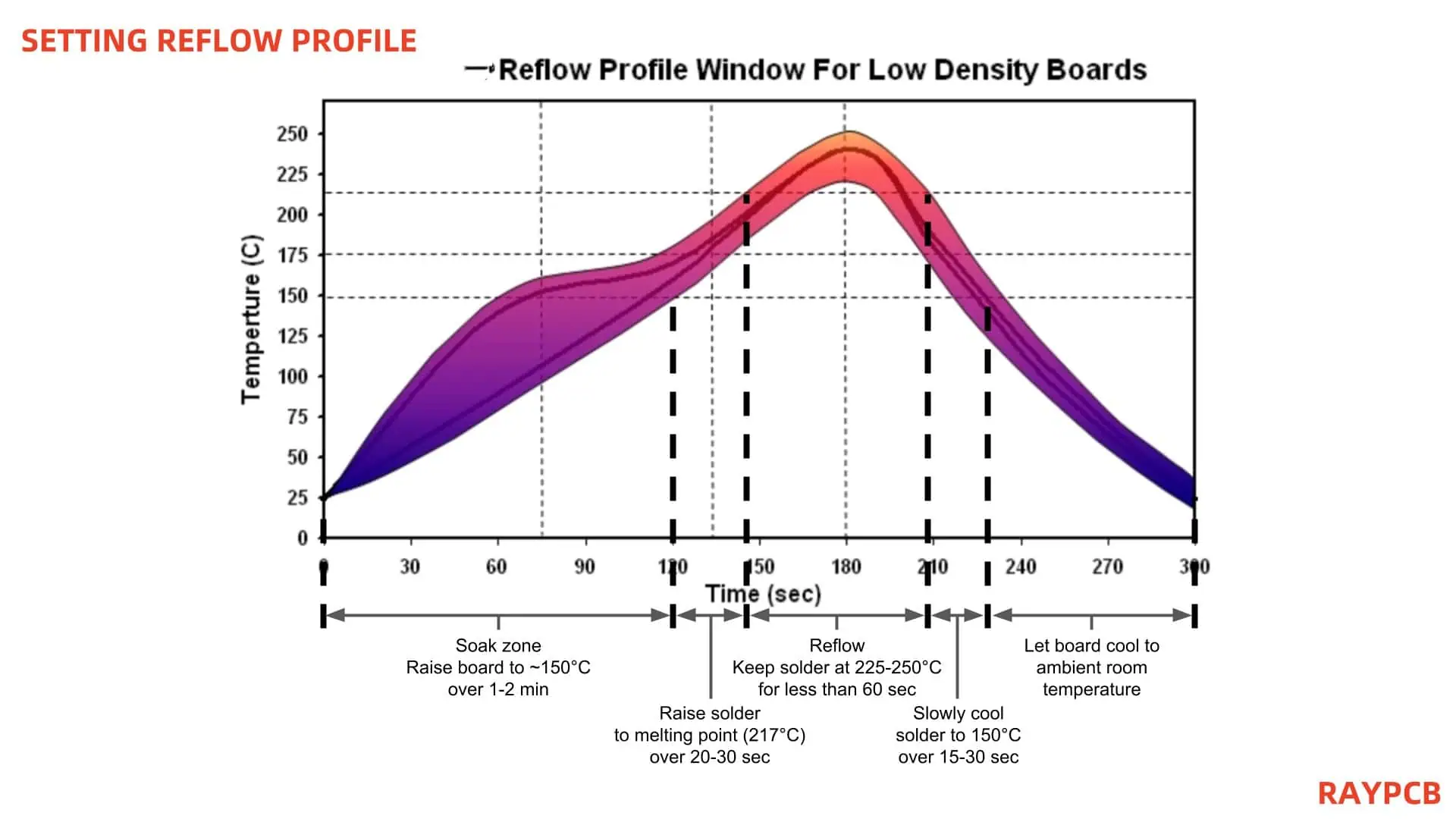
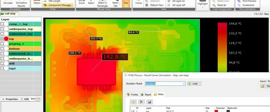
Thermal testing becomes particularly important for precision analog circuits where temperature coefficients can significantly impact performance. Understanding how component values drift with temperature and designing appropriate compensation helps maintain accuracy across the operating temperature range.

Manufacturing and Assembly Considerations

The manufacturing process itself can impact analog circuit performance. PCB fabrication tolerances affect trace impedances and component placement accuracy. Assembly processes introduce thermal stress that can shift component values, particularly affecting precision resistors and capacitors.

Solder joint quality becomes critical for high-frequency analog circuits where even small discontinuities can cause reflections and losses. Proper solder mask design and assembly procedures help ensure reliable connections.

Future Trends and Emerging Technologies

The evolution of analog PCB design continues with advancing technologies and changing requirements. Higher integration levels push more analog functionality into specialized integrated circuits, reducing discrete component count but increasing the importance of power supply design and thermal management.

Advanced PCB materials continue to emerge, offering better electrical properties and thermal performance. Embedded component technologies allow passive components to be integrated directly into the PCB substrate, reducing parasitic effects and improving performance.

The increasing prevalence of high-speed digital interfaces requires analog designers to consider signal integrity effects that were previously confined to digital design domains. Understanding transmission line theory, impedance matching, and electromagnetic compatibility becomes essential for modern analog designers.

In conclusion, successful analog PCB design requires a deep understanding of the complex interactions between circuit topology, component placement, routing strategies, and manufacturing processes. The PCB becomes an active participant in circuit performance rather than simply a mechanical support structure. As electronic systems continue to demand higher performance, lower noise, and smaller form factors, the importance of masterful analog PCB design will only continue to grow.

Guidelines to Identify Hottest and Coldest Spots on PCBA for Setting Reflow Profile

The successful assembly of printed circuit board assemblies (PCBAs) through surface mount technology (SMT) reflow soldering depends critically on achieving uniform temperature distribution across the entire board during the reflow process. Identifying the hottest and coldest spots on a PCBA is essential for establishing an optimal reflow profile that ensures proper solder joint formation while preventing component damage from thermal stress. This comprehensive guide outlines the systematic approach to thermal characterization and profile optimization.

YouTube video

Understanding Thermal Variations in PCBA Design

Temperature variations across a PCBA during reflow occur due to several factors including board geometry, component density, copper distribution, and thermal mass differences. Areas with high component density or large copper pours typically act as heat sinks, creating cooler zones, while thin sections with minimal copper coverage tend to heat up more rapidly. The challenge lies in balancing these thermal differences to achieve consistent solder joint quality across all components.

The thermal behavior of a PCBA is influenced by its physical characteristics, including board thickness, layer count, and material composition. Multi-layer boards with extensive internal copper layers exhibit different thermal properties compared to simple two-layer designs. High-frequency boards using specialized substrates like Rogers materials may have unique thermal characteristics that differ from standard FR4 constructions. Understanding these fundamental properties forms the foundation for effective thermal profiling.

Pre-Profiling Board Analysis

Before beginning thermal measurements, conduct a thorough visual and design analysis of the PCBA. Identify areas with varying component densities, noting regions with large components such as connectors, transformers, or heat sinks that may act as thermal masses. Examine the copper distribution pattern, paying attention to ground planes, power planes, and routing density variations. Areas with extensive copper coverage will typically exhibit slower heating and cooling rates compared to regions with minimal copper.

Component placement analysis should focus on identifying potential thermal shadows and heat concentration zones. Large components can shield smaller components from direct heating, creating temperature gradients that may affect solder joint formation. Conversely, areas with high power dissipation components may experience elevated temperatures that require careful monitoring to prevent overheating.

Consider the board’s entry and exit points in the reflow oven, as these areas often experience different thermal profiles due to conveyor effects and oven zone transitions. Edge effects can create temperature variations that impact components near board boundaries differently than those in central locations.

Temperature Measurement Techniques

Thermocouple placement represents the most common and reliable method for PCBA thermal profiling. Use Type K thermocouples with appropriate bead sizes for the measurement scale required. Smaller beads provide more accurate point measurements but may be more fragile during handling. Position thermocouples using high-temperature adhesive or specialized clips that maintain good thermal contact without creating thermal bridges.

Strategic thermocouple placement should cover representative areas across the board, including suspected hot and cold spots identified during the design analysis phase. Typically, six to twelve measurement points provide adequate coverage for most PCBAs, though complex designs may require additional sensors. Place thermocouples on component leads or pads rather than bare copper or solder mask to better represent actual solder joint temperatures.

Infrared thermal imaging offers an alternative or complementary approach to thermocouple measurements. Thermal cameras can provide comprehensive temperature mapping across the entire PCBA surface, revealing thermal patterns that might be missed with point measurements. However, emissivity variations across different surface materials can affect measurement accuracy, requiring careful calibration and interpretation.

Systematic Profiling Methodology

Begin thermal profiling with a baseline reflow profile based on solder paste manufacturer recommendations and component thermal requirements. This initial profile serves as a starting point for optimization rather than a final solution. Run the board through the reflow process while monitoring all measurement points simultaneously, recording temperature data at sufficient resolution to capture thermal transitions.

Analyze the collected data to identify temperature spreads across measurement points during critical reflow phases. Pay particular attention to the preheat phase, where thermal equilibration occurs, and the reflow phase, where peak temperatures must be achieved uniformly. Calculate the temperature difference between the hottest and coldest points at each phase to quantify thermal uniformity.

Document any temperature excursions beyond component specifications or solder paste requirements at individual measurement points. Components with lower thermal tolerance may require special attention in profile development, potentially necessitating compromise solutions that balance optimal solder joint formation with component survival.

Identifying Critical Temperature Zones

Hot spots typically occur in areas with minimal thermal mass, thin copper traces, or direct exposure to oven heating elements. These locations may include board edges, areas between large components, or regions with sparse component population. Hot spots pose risks of component overheating, solder balling, or excessive intermetallic formation that can compromise joint reliability.

Cold spots commonly develop in areas with high thermal mass, dense component placement, or significant copper coverage. Large ground planes, connector areas, and regions with multiple large components often exhibit slower temperature rise and may not reach adequate reflow temperatures. Insufficient heating in these areas can result in incomplete solder joint formation, poor wetting, or cold solder joints.

Thermal shadows occur when large components shield adjacent smaller components from direct heating. These shadows can create localized cold spots that require profile adjustments to ensure adequate heat transfer. Similarly, thermal bridges between large thermal masses can create temperature gradients that affect multiple components simultaneously.

Profile Optimization Strategies

Once hot and cold spots are identified, implement targeted profile adjustments to improve thermal uniformity. Extend preheat zones to allow better thermal equilibration, particularly for boards with significant thermal mass variations. Longer preheat phases help reduce temperature differentials before entering the critical reflow zone.

Adjust conveyor speed to modify the overall thermal exposure time. Slower speeds increase total heat input but may also increase temperature spreads if heating is non-uniform. Conversely, faster speeds may help prevent overheating in hot spots but could result in insufficient heating in cold areas.

Oven zone temperature adjustments should be made incrementally, monitoring the effect on both hot and cold spots. Increasing temperatures in zones corresponding to cold spot locations may help improve heating in those areas, but careful monitoring ensures hot spots don’t exceed safe limits. Some ovens allow for cross-zone adjustments or nitrogen atmosphere control that can help achieve better thermal uniformity.

Validation and Iterative Refinement

After implementing profile changes, repeat the thermal measurement process to verify improvements in temperature uniformity. Compare new data against previous measurements to quantify the effectiveness of adjustments. Look for reductions in temperature spread between hot and cold spots while ensuring all areas meet minimum temperature requirements.

Perform multiple validation runs to ensure profile repeatability and consistency. Thermal variations can occur due to oven warm-up conditions, ambient temperature changes, or minor process variations. Statistical analysis of multiple runs provides confidence in profile stability and identifies any remaining thermal uniformity issues.

Consider running worst-case scenarios such as fully loaded production panels or boards with maximum component population to validate profile robustness under actual production conditions. These validation runs often reveal thermal issues not apparent in prototype or lightly loaded test conditions.

Advanced Considerations and Troubleshooting

For complex PCBAs with persistent thermal uniformity challenges, consider advanced solutions such as selective heating using focused infrared sources or localized preheating stations. These approaches can address specific cold spots without affecting the overall thermal profile.

Process modifications such as stencil design optimization, solder paste selection, or component placement adjustments may be necessary when thermal profiling reveals fundamental design issues. Collaboration between design, manufacturing, and process engineering teams often yields innovative solutions to challenging thermal uniformity problems.

Documentation of final profiles should include detailed measurement data, thermocouple placement diagrams, and specific oven settings for future reference and process control. This documentation serves as the foundation for process monitoring and troubleshooting when thermal issues arise during production.

The systematic identification and characterization of thermal variations in PCBA reflow processing ensures reliable solder joint formation while protecting components from thermal damage. Through careful measurement, analysis, and iterative optimization, manufacturers can achieve robust reflow profiles that deliver consistent assembly quality across diverse board designs and component configurations.

IMPORTANT PCB TERMINOLOGY FOR BEGINNERS

Printed Circuit Boards (PCBs) are the backbone of modern electronics, serving as the foundation for countless devices we use daily. For beginners entering the world of electronics and PCB design, understanding the terminology is crucial. This comprehensive guide will introduce you to the most important PCB terms, helping you navigate the complexities of circuit board design and manufacturing.

Basic PCB Components

1. Substrate

The substrate is the base material of a PCB, providing mechanical support and insulation for the conductive layers.

Common Substrate Materials

MaterialAdvantagesDisadvantages
FR-4 (Flame Retardant 4)Cost-effective, good electrical propertiesNot suitable for high-frequency applications
PolyimideHigh temperature resistance, flexibleExpensive
CeramicExcellent thermal conductivityBrittle, expensive
PTFE (Teflon)Low dielectric constant, suitable for high-frequencyExpensive, difficult to process

2. Copper Layers

Copper layers are the conductive paths on a PCB that carry electrical signals and power.

Types of PCBs Based on Copper Layers

RF Multiplexer
RF Multiplexer
TypeDescriptionCommon Applications
Single-sidedOne copper layerSimple electronics, low-cost products
Double-sidedTwo copper layersConsumer electronics, industrial controls
MultilayerFour or more copper layersComplex electronics, high-speed digital devices

3. Solder Mask

The solder mask is a thin layer of polymer applied to the PCB surface to protect copper traces from oxidation and prevent solder bridges during assembly.

4. Silkscreen

The silkscreen is a layer of text and symbols printed on the PCB surface to provide information about component placement, board identification, and warnings.

PCB Design Terms

1. Schematic

A schematic is a diagram that represents the electrical connections and components of a circuit using standardized symbols.

2. Layout

The layout is the physical arrangement of components and traces on the PCB.

3. Footprint

A footprint is the physical representation of a component on the PCB, including its size, shape, and pad arrangement.

4. Trace

Traces are the conductive paths on a PCB that connect components and carry electrical signals.

Trace Width Guidelines

Current CapacityRecommended Trace Width
Up to 1A10 mil (0.254 mm)
1A to 2A20 mil (0.508 mm)
2A to 3A30 mil (0.762 mm)
3A to 4A40 mil (1.016 mm)
4A to 5A50 mil (1.27 mm)

5. Via

A via is a plated hole that connects traces on different layers of a multilayer PCB.

Types of Vias

TypeDescriptionAdvantages
Through-holeExtends through all layersSimple to manufacture
BlindConnects outer layer to inner layerIncreases routing density
BuriedConnects inner layers onlyMaximizes board space
Micro viaVery small diameter (typically <0.15mm)High-density designs

6. Pad

A pad is a conductive area on the PCB where component leads or surface-mount devices are soldered.

7. Plane

A plane is a large area of copper on a PCB layer, typically used for power distribution or grounding.

PCB Manufacturing Terms

1. Gerber Files

Gerber files are the standard format for PCB manufacturing data, containing information about copper layers, solder mask, silkscreen, and drill locations.

2. Drill File

A drill file specifies the location, size, and type of holes to be drilled in the PCB.

3. Etching

Etching is the process of removing unwanted copper from the PCB to create the desired circuit pattern.

4. Plating

Plating is the process of depositing a thin layer of metal (usually copper) onto the PCB surface and in drilled holes.

5. Solder Paste

Solder paste is a mixture of tiny solder particles and flux used for surface-mount component assembly.

Advanced PCB Concepts

1. Impedance Control

Impedance control is the practice of designing traces with specific electrical characteristics to maintain signal integrity in high-speed circuits.

Common Controlled Impedance Values

ApplicationTypical Impedance
Digital circuits50ฮฉ or 100ฮฉ
RF circuits50ฮฉ or 75ฮฉ
Differential pairs100ฮฉ or 120ฮฉ

2. EMI/EMC

Electromagnetic Interference (EMI) and Electromagnetic Compatibility (EMC) refer to the ability of electronic devices to function without interfering with other devices and to withstand interference from external sources.

3. Thermal Management

Thermal management involves designing PCBs to effectively dissipate heat generated by components.

Thermal Management Techniques

TechniqueDescription
Heat sinksAttach to components to increase surface area for heat dissipation
Thermal viasConduct heat from one PCB layer to another
Copper poursLarge areas of copper to spread heat across the board
Thermal reliefConnect pads to planes while limiting heat transfer during soldering

4. High-Speed Design

High-speed design involves techniques to maintain signal integrity in circuits operating at high frequencies or with fast edge rates.

Key High-Speed Design Considerations

ConsiderationDescription
Impedance matchingEnsuring trace impedance matches source and load impedances
Signal terminationAdding resistors to prevent reflections on transmission lines
Differential routingRouting pairs of traces to carry complementary signals
Crosstalk minimizationControlling coupling between adjacent traces

5. Flex and Rigid-Flex PCBs

Flex PCBs are made with flexible materials, allowing them to bend or fold. Rigid-flex PCBs combine rigid and flexible sections in a single board.

Applications of Flex and Rigid-Flex PCBs

TypeCommon Applications
Flex PCBsWearable devices, medical implants, folded electronics
Rigid-Flex PCBsAerospace, military equipment, compact consumer electronics

PCB Assembly Terms

1. SMT (Surface Mount Technology)

SMT is a method of mounting components directly onto the surface of a PCB, as opposed to through-hole technology.

2. THT (Through-Hole Technology)

THT involves inserting component leads through holes in the PCB and soldering them on the opposite side.

3. Reflow Soldering

Reflow soldering is a process used in SMT assembly where solder paste is heated to create solder joints.

Typical Reflow Soldering Profile

PhaseTemperature RangeDuration
Preheat150-200ยฐC60-120 seconds
Soak150-200ยฐC60-120 seconds
Reflow220-250ยฐC30-60 seconds
CoolingBelow 150ยฐC60-120 seconds

4. Wave Soldering

Wave soldering is a bulk soldering process primarily used for through-hole components, where the PCB passes over a wave of molten solder.

5. Pick and Place

Pick and place refers to the automated process of placing SMT components onto a PCB using specialized machinery.

PCB Testing and Quality Assurance

1. AOI (Automated Optical Inspection)

AOI uses cameras and image processing software to inspect PCBs for defects such as missing components, incorrect placement, or solder issues.

2. ICT (In-Circuit Testing)

ICT involves using a bed-of-nails fixture to make contact with specific points on a PCB to test for shorts, opens, and component values.

3. Functional Testing

Functional testing verifies that the assembled PCB performs its intended functions correctly.

4. Flying Probe Testing

Flying probe testing uses moving probes to make contact with specific points on the PCB, allowing for more flexible testing than ICT.

Frequently Asked Questions (FAQ)

  1. Q: What is the difference between FR-4 and FR-1 substrate materials? A: FR-4 is a glass-reinforced epoxy laminate, while FR-1 is a paper-based phenolic resin material. FR-4 is more durable, has better electrical properties, and is more commonly used in modern PCBs. FR-1 is less expensive but is limited to simpler, low-cost applications.
  2. Q: How do I choose between single-sided, double-sided, and multilayer PCBs? A: The choice depends on your circuit complexity and application requirements. Single-sided PCBs are suitable for simple circuits and low-cost products. Double-sided PCBs offer more routing options and are good for medium-complexity designs. Multilayer PCBs are necessary for complex circuits, high-speed designs, and when space is limited.
  3. Q: What is the purpose of a ground plane in a PCB? A: A ground plane serves several important functions: it provides a low-impedance return path for electrical signals, reduces electromagnetic interference (EMI), improves heat dissipation, and simplifies routing by allowing components to be grounded easily.
  4. Q: How can I minimize crosstalk in my PCB design? A: To minimize crosstalk, you can: increase the spacing between parallel traces, use ground planes or guard traces to shield sensitive signals, minimize the length of parallel runs, and use differential signaling for critical high-speed signals.
  5. Q: What is the significance of impedance control in PCB design? A: Impedance control is crucial for maintaining signal integrity in high-speed circuits. It ensures that signals propagate through the PCB without reflections or distortions, which is especially important for digital circuits operating at high frequencies or with fast edge rates. Controlled impedance traces are designed to match the impedance of the source and load, typically 50ฮฉ or 100ฮฉ for digital circuits.

What Are FFC, BTB & Flying Connectors and Their Role in PCB Boards?

In the world of electronics and printed circuit board (PCB) design, connectors play a crucial role in facilitating electrical connections between different components and boards. Among the various types of connectors available, Flexible Flat Cable (FFC), Board-to-Board (BTB), and Flying connectors stand out for their unique characteristics and applications. This comprehensive article will delve into the intricacies of these connectors, exploring their designs, functions, advantages, and roles in modern PCB assemblies.

Understanding Connectors in PCB Design

Before we dive into the specific types of connectors, it’s essential to understand the broader context of connectors in PCB design.

The Importance of Connectors

Connectors serve as the bridge between different electronic components, boards, and systems. They enable:

  1. Signal transmission
  2. Power distribution
  3. Data transfer
  4. Modular design and assembly
  5. Easy maintenance and replacement of components

Key Factors in Connector Selection

When choosing connectors for a PCB design, several factors must be considered:

  1. Electrical requirements (current, voltage, signal integrity)
  2. Mechanical constraints (size, shape, mating force)
  3. Environmental conditions (temperature, humidity, vibration)
  4. Reliability and durability
  5. Cost and availability
  6. Ease of assembly and maintenance

With this foundation, let’s explore FFC, BTB, and Flying connectors in detail.

Flexible Flat Cable (FFC) Connectors

What are FFC Connectors?

Flexible Flat Cable (FFC) connectors are designed to work with flat, flexible cables that contain multiple conducting strips running parallel to each other. These connectors are known for their low profile and ability to fit in tight spaces.

Key Characteristics of FFC Connectors

CharacteristicDescription
Cable TypeFlat, flexible with parallel conductors
ProfileLow and compact
PitchTypically 0.5mm to 1.25mm
Number of PinsRanges from 4 to 60+
Mating StyleZIF (Zero Insertion Force) or non-ZIF
FlexibilityHigh, allows for dynamic applications

Advantages of FFC Connectors

  1. Space-saving design
  2. Flexibility for use in moving parts
  3. Good EMI/RFI shielding when properly designed
  4. Cost-effective for high-volume production
  5. Reliable performance in high-flex applications

Applications of FFC Connectors

FFC connectors find widespread use in:

  1. LCD displays and touch panels
  2. Printers and scanners
  3. Automotive dashboard electronics
  4. Mobile devices and laptops
  5. Medical equipment

Challenges and Considerations

While FFC connectors offer numerous advantages, they also present some challenges:

  1. Careful handling required to prevent damage
  2. Potential for signal degradation over long distances
  3. Limited current-carrying capacity compared to some alternatives
  4. Requires proper strain relief to prevent disconnection

Board-to-Board (BTB) Connectors

What are BTB Connectors?

Board-to-Board (BTB) connectors, as the name suggests, are designed to connect two PCBs directly to each other. They come in various styles to accommodate different board orientations and spacing requirements.

Types of BTB Connectors

  1. Mezzanine Connectors: For parallel board stacking
  2. Card Edge Connectors: One board plugs directly into another
  3. Backplane Connectors: For connecting multiple boards to a main backplane
  4. High-Speed BTB Connectors: Designed for high-frequency signal transmission

Key Characteristics of BTB Connectors

CharacteristicDescription
OrientationParallel, perpendicular, or angled
PitchRanges from 0.4mm to 2.54mm
Number of PinsCan exceed 1000 for high-density applications
Stack HeightFrom <5mm to >30mm
Signal IntegrityOften designed for high-speed data transmission
Current CapacityVaries widely based on design

Advantages of BTB Connectors

  1. Enable compact, 3D PCB designs
  2. High-density interconnections
  3. Eliminate the need for cables in many applications
  4. Can be designed for high-speed signal transmission
  5. Available in various styles to suit different design requirements

Applications of BTB Connectors

BTB connectors are widely used in:

  1. Telecommunications equipment
  2. Server and data center hardware
  3. Industrial control systems
  4. Automotive electronics
  5. Consumer electronics (smartphones, tablets)

Challenges and Considerations

When working with BTB connectors, designers must consider:

  1. Mechanical stress and vibration tolerance
  2. Thermal management in high-density designs
  3. Signal integrity for high-speed applications
  4. Assembly and rework processes
  5. Cost implications for high-pin-count connectors

Flying Connectors

What are Flying Connectors?

Flying connectors, also known as flying leads or wire-to-board connectors, consist of a connector attached to the end of a wire or cable. They provide a flexible means of connecting PCBs to other components or boards.

Types of Flying Connectors

  1. Crimp-style connectors: Wires are crimped to contacts
  2. IDC (Insulation Displacement Connector): Contacts pierce the wire insulation
  3. Soldered flying leads: Wires are soldered directly to the connector
  4. Plug-and-socket systems: Modular connectors with mating plugs and sockets

Key Characteristics of Flying Connectors

CharacteristicDescription
Wire TypeSingle-core or multi-stranded
Wire GaugeTypically 18-30 AWG
Connector StyleVarious (crimp, IDC, modular)
FlexibilityHigh, allows for versatile connections
Current CapacityDepends on wire gauge and connector design
Strain ReliefOften incorporated to protect connections

Advantages of Flying Connectors

  1. Flexibility in board-to-device connections
  2. Ease of assembly and field replacements
  3. Can accommodate movements and vibrations
  4. Useful for prototyping and custom designs
  5. Allow for connections between boards at different angles or distances

Applications of Flying Connectors

Flying connectors are commonly used in:

  1. Automotive wiring harnesses
  2. Home appliances
  3. Industrial control panels
  4. Aerospace and defense equipment
  5. Medical devices

Challenges and Considerations

When using flying connectors, designers should be aware of:

  1. Potential for increased electromagnetic interference (EMI)
  2. Need for proper strain relief and wire management
  3. Quality control in crimping or soldering processes
  4. Space requirements for wire routing
  5. Potential for human error during manual assembly

Comparing FFC, BTB, and Flying Connectors

To better understand the strengths and weaknesses of each connector type, let’s compare them across several key factors:

FactorFFC ConnectorsBTB ConnectorsFlying Connectors
Space EfficiencyHighVery HighModerate
FlexibilityHighLowHigh
Signal IntegrityGoodExcellentModerate
Ease of AssemblyModerateModerateHigh
CostLow to ModerateModerate to HighLow to Moderate
DurabilityModerateHighModerate
Current CapacityLow to ModerateModerate to HighVaries
EMI ShieldingGoodExcellentPoor to Moderate

Design Considerations and Best Practices

When incorporating FFC, BTB, or Flying connectors into PCB designs, consider the following best practices:

For FFC Connectors

  1. Ensure proper alignment and insertion of the cable
  2. Use strain relief to prevent cable damage
  3. Consider EMI shielding for sensitive applications
  4. Choose the appropriate pitch and number of conductors for the application
  5. Be mindful of the minimum bend radius of the flexible cable

For BTB Connectors

  1. Account for mechanical stress and vibration in the design
  2. Consider thermal management, especially in high-density designs
  3. Use appropriate stack height for the application
  4. Ensure proper alignment between mating connectors
  5. Consider signal integrity requirements for high-speed applications

For Flying Connectors

  1. Implement proper strain relief and wire management
  2. Use appropriate wire gauge for current requirements
  3. Consider modular designs for ease of maintenance
  4. Ensure proper crimping or soldering techniques are used
  5. Account for EMI considerations in sensitive circuits

Future Trends in Connector Technology

As electronics continue to evolve, connector technology is adapting to meet new challenges:

  1. Miniaturization: Connectors are becoming smaller while maintaining or improving performance.
  2. Higher Data Rates: Development of connectors capable of handling ever-increasing data transmission speeds.
  3. Improved Power Handling: Connectors that can manage higher currents in compact designs.
  4. Environmental Considerations: Focus on recyclable and eco-friendly connector materials.
  5. Smart Connectors: Integration of sensors and diagnostic capabilities within connectors.

Frequently Asked Questions (FAQ)

Q1: Can FFC connectors be used in high-vibration environments?

A1: While FFC connectors can be used in environments with some vibration, they are generally not the best choice for high-vibration applications. In such environments, it’s crucial to use proper strain relief and consider alternatives like ruggedized BTB connectors or specialized flying connectors designed for high-vibration scenarios. If FFC connectors must be used, additional mechanical support and vibration dampening measures should be implemented.

Q2: How do I choose between BTB connectors and flying connectors for my design?

A2: The choice between BTB and flying connectors depends on several factors:

  1. Space constraints: BTB connectors are generally more space-efficient.
  2. Flexibility requirements: Flying connectors offer more flexibility in positioning and movement.
  3. Signal integrity: BTB connectors typically offer better signal integrity for high-speed applications.
  4. Assembly process: Flying connectors can be easier to assemble and replace in the field.
  5. Cost considerations: BTB connectors can be more expensive, especially for high-pin-count applications.

Consider these factors in the context of your specific application to make the best choice.

Q3: Are there waterproof versions of FFC, BTB, and flying connectors?

A3: Yes, waterproof or water-resistant versions are available for all three connector types:

  1. FFC: Some manufacturers offer waterproof FFC connectors with IP67 or IP68 ratings.
  2. BTB: Sealed BTB connectors are available for harsh environment applications.
  3. Flying Connectors: Many flying connectors are designed with environmental sealing for use in automotive and outdoor applications.

When selecting waterproof connectors, ensure they meet the specific ingress protection (IP) rating required for your application.

Q4: How do I ensure signal integrity when using long FFC cables?

A4: To maintain signal integrity with long FFC cables:

  1. Use shielded FFC cables for sensitive signals.
  2. Implement proper grounding and shielding techniques.
  3. Consider using differential signaling for critical high-speed signals.
  4. Minimize the cable length where possible.
  5. Use signal conditioning or repeater circuits for very long runs.
  6. Choose FFCs with appropriate impedance characteristics for your application.

For very long distances or high-speed signals, consider alternatives like optical interconnects.

Q5: Can I mix different types of connectors in my PCB design?

A5: Yes, it’s common to use a combination of connector types in complex PCB designs. Each connector type has its strengths, and using a mix can optimize the overall design. For example:

  1. BTB connectors for high-density board-to-board connections
  2. FFC connectors for connecting to displays or flexible components
  3. Flying connectors for external device connections or where flexibility is needed

When mixing connector types, ensure compatibility in terms of signal levels, power requirements, and overall system design. Also, consider the assembly process and maintenance procedures when using multiple connector types.

In conclusion, FFC, BTB, and Flying connectors each play vital roles in modern PCB design. Understanding their characteristics, advantages, and limitations is crucial for creating efficient, reliable, and cost-effective electronic systems. As technology continues to advance, these connector types will evolve, offering new possibilities for innovative electronic designs.

Advantages of G10 Epoxy Substrate

G10 epoxy substrate, also known as FR-4 (Flame Retardant 4), is a versatile and widely used material in various industries, particularly in the electronics and electrical engineering sectors. This high-performance composite material consists of a woven fiberglass cloth impregnated with an epoxy resin binder. Its unique combination of properties has made it a popular choice for numerous applications, from printed circuit boards (PCBs) to industrial components. In this comprehensive article, we will explore the numerous advantages of G10 epoxy substrate, its applications, and why it continues to be a preferred material in many industries.

Composition and Manufacturing Process

Chemical Composition

G10 epoxy substrate is composed of two main components:

  1. Fiberglass cloth: Provides structural strength and stability
  2. Epoxy resin: Acts as a binding agent and imparts specific properties

The exact composition may vary slightly depending on the manufacturer and specific grade, but the basic structure remains consistent.

Manufacturing Process

The production of G10 epoxy substrate involves several steps:

  1. Weaving of fiberglass cloth
  2. Impregnation of the cloth with epoxy resin
  3. Partial curing (B-staging)
  4. Layering of multiple sheets
  5. Final curing under heat and pressure

This process results in a dense, uniform material with excellent mechanical and electrical properties.

Key Properties of G10 Epoxy Substrate

G10 epoxy substrate boasts an impressive array of properties that contribute to its widespread use. Let’s examine these properties in detail:

Mechanical Properties

PropertyValue RangeUnit
Tensile Strength250 – 490MPa
Flexural Strength340 – 560MPa
Compressive Strength380 – 480MPa
Impact Strength65 – 80kJ/mยฒ
Hardness (Rockwell M)100 – 110

These mechanical properties make G10 epoxy substrate suitable for applications requiring high strength and durability.

Electrical Properties

PropertyValue RangeUnit
Dielectric Strength20 – 28kV/mm
Dielectric Constant (at 1 MHz)4.0 – 5.5
Dissipation Factor (at 1 MHz)0.016 – 0.020
Volume Resistivity10^9 – 10^12ฮฉยทcm
Surface Resistivity10^9 – 10^11ฮฉ 

The excellent electrical insulation properties of G10 make it ideal for use in electrical and electronic applications.

Thermal Properties

PropertyValue RangeUnit
Thermal Conductivity0.25 – 0.35W/mยทK
Coefficient of Thermal Expansion11.-15ppm/ยฐC
Glass Transition Temperature (Tg)130 – 180ยฐC
Maximum Operating Temperature130 – 150ยฐC

G10’s thermal properties allow it to maintain stability and performance across a wide temperature range.

Advantages of G10 Epoxy Substrate

Now that we’ve examined the key properties of G10 epoxy substrate, let’s delve into its numerous advantages:

1. High Strength-to-Weight Ratio

G10 epoxy substrate offers exceptional strength while remaining relatively lightweight. This combination makes it ideal for applications where weight reduction is crucial without compromising structural integrity.

2. Excellent Electrical Insulation

The high dielectric strength and low dissipation factor of G10 make it an outstanding electrical insulator. This property is particularly valuable in the production of printed circuit boards and other electronic components.

3. Dimensional Stability

G10 exhibits minimal warping, shrinkage, or expansion under varying environmental conditions. This stability is crucial for maintaining precise tolerances in manufacturing processes and ensuring consistent performance in final products.

4. Chemical Resistance

The epoxy resin in G10 provides good resistance to a wide range of chemicals, including oils, fuels, and many solvents. This resistance helps protect the material and any components it houses from environmental degradation.

5. Flame Retardancy

As indicated by its alternative name (FR-4), G10 epoxy substrate has inherent flame-retardant properties. This characteristic is essential for safety in electrical and electronic applications, helping to prevent the spread of fires.

6. Low Moisture Absorption

G10 has a low tendency to absorb moisture, which helps maintain its electrical and mechanical properties even in humid environments. This property is particularly important for applications in aerospace and marine industries.

7. Machinability

Despite its high strength, G10 can be easily machined using standard tools and processes. This machinability allows for the creation of complex shapes and precise components without specialized equipment.

8. Temperature Resistance

With a relatively high glass transition temperature and good thermal stability, G10 can maintain its properties across a wide range of operating temperatures. This makes it suitable for use in challenging thermal environments.

9. Versatility

G10 epoxy substrate can be manufactured in various grades and thicknesses, allowing it to be tailored for specific applications. This versatility makes it a go-to material for engineers and designers across multiple industries.

10. Cost-Effectiveness

Compared to some high-performance materials with similar properties, G10 offers a good balance of performance and cost. Its widespread availability and established manufacturing processes contribute to its cost-effectiveness.

Applications of G10 Epoxy Substrate

The unique combination of properties offered by G10 epoxy substrate makes it suitable for a wide range of applications across various industries. Let’s explore some of the most common uses:

1. Electronics and Electrical Engineering

Printed Circuit Boards (PCBs)

G10/FR-4 is the standard material for PCB manufacturing due to its excellent electrical properties, dimensional stability, and ease of processing.

Electrical Insulators

The high dielectric strength of G10 makes it ideal for creating insulators in various electrical components and systems.

Terminal Boards

G10 is often used in the production of terminal boards for electrical connections due to its insulating properties and mechanical strength.

2. Aerospace and Defense

Structural Components

The high strength-to-weight ratio of G10 makes it suitable for various structural components in aircraft and spacecraft.

Radomes

G10’s electrical properties and weather resistance make it an excellent material for radar domes (radomes) used in both civilian and military applications.

Missile Components

The material’s combination of strength, lightweight, and thermal resistance is valuable in missile guidance systems and structural parts.

3. Automotive Industry

Electrical Components

G10 is used in various electrical components within vehicles, including circuit boards for engine control units and other electronic systems.

Thermal Insulators

The low thermal conductivity of G10 makes it useful for creating thermal barriers in automotive applications.

4. Industrial Manufacturing

Machined Parts

G10’s machinability allows for the creation of precise, custom components for various industrial applications.

Wear Plates

The material’s durability and low friction properties make it suitable for use as wear plates in machinery and equipment.

Fixtures and Jigs

G10’s dimensional stability and strength make it ideal for creating fixtures and jigs used in manufacturing processes.

5. Marine Industry

Electrical Panels

The material’s resistance to moisture and chemicals makes it suitable for electrical panels and components in marine environments.

Structural Components

G10 is used in various structural applications in boats and ships due to its strength and resistance to environmental factors.

6. Oil and Gas Industry

Downhole Components

G10’s chemical resistance and strength make it suitable for various components used in oil and gas exploration and extraction.

Insulating Flanges

The material’s electrical insulation properties are valuable in creating insulating flanges for pipelines and other equipment.

Comparing G10 to Other Materials

To better understand the advantages of G10 epoxy substrate, it’s useful to compare it with other materials commonly used in similar applications:

PropertyG10 EpoxyAluminumPolyethyleneBakelite
Density (g/cmยณ)1.7 – 1.92.70.91 – 0.971.3 – 1.4
Tensile Strength (MPa)250 – 49070 – 70010 – 4025 – 55
Dielectric Strength (kV/mm)20 – 28N/A (conductor)20 – 8015 – 20
Thermal Conductivity (W/m่ทฏK)0.25 – 0.35205 – 2500.33 – 0.520.15 – 0.25
Maximum Operating Temp (ๆŽณC)130 – 150150 – 20080 – 120120 – 150
Chemical ResistanceGoodModerateExcellentGood
CostModerateLow to ModerateLowLow

This comparison highlights G10’s balanced combination of properties, making it a versatile choice for many applications.

Limitations and Considerations

While G10 epoxy substrate offers numerous advantages, it’s important to be aware of its limitations:

  1. Relatively High Cost: Compared to some basic materials, G10 can be more expensive, which may impact its use in cost-sensitive applications.
  2. Limited High-Temperature Performance: While G10 performs well at moderate temperatures, it may not be suitable for extreme high-temperature environments.
  3. Potential for Moisture Absorption: Although G10 has low moisture absorption compared to many materials, prolonged exposure to humid environments can still affect its properties.
  4. Difficulty in Recycling: The composite nature of G10 makes it challenging to recycle, which may be a consideration in environmentally-sensitive applications.
  5. Dust Generation During Machining: Machining G10 can produce fine dust, requiring proper safety measures and dust collection systems.

Future Developments and Trends

As technology advances, we can expect to see continued improvements and innovations in G10 epoxy substrate and related materials:

  1. Enhanced Thermal Management: Development of G10 variants with improved thermal conductivity for better heat dissipation in electronic applications.
  2. Eco-Friendly Formulations: Research into more environmentally friendly epoxy resins and manufacturing processes to address recycling concerns.
  3. Nanocomposite Enhancements: Incorporation of nanoparticles to further improve mechanical, electrical, or thermal properties.
  4. Tailored Properties: Development of G10 variants with properties optimized for specific applications or industries.
  5. Integration with Advanced Manufacturing: Exploration of how G10 can be integrated into additive manufacturing processes for complex geometries.

Frequently Asked Questions (FAQ)

Q1: What is the difference between G10 and FR-4?

A1: G10 and FR-4 are essentially the same material. FR-4 (Flame Retardant 4) is the designation given to G10 when it meets specific flame retardancy standards set by the National Electrical Manufacturers Association (NEMA). In practice, the terms are often used interchangeably, especially in the context of printed circuit board materials.

Q2: Can G10 epoxy substrate be used outdoors?

A2: Yes, G10 epoxy substrate can be used in outdoor applications. It has good resistance to moisture, UV radiation, and various environmental factors. However, for prolonged outdoor exposure, it’s advisable to use grades specifically formulated for outdoor use or to apply additional protective coatings to enhance its weather resistance.

Q3: How does G10 compare to carbon fiber composites?

A3: While both G10 and carbon fiber composites are high-performance materials, they have different strengths:

  • G10 is generally less expensive and easier to machine.
  • Carbon fiber composites typically offer higher strength-to-weight ratios and better fatigue resistance.
  • G10 has better electrical insulation properties.
  • Carbon fiber composites usually have superior stiffness and vibration damping characteristics.

The choice between the two depends on the specific requirements of the application.

Q4: Is G10 epoxy substrate food safe?

A4: Standard G10 epoxy substrate is not typically considered food safe. However, there are specialized grades of epoxy composites that are formulated to be compliant with food safety regulations. If food contact is required, it’s essential to use materials specifically certified for food safety applications.

Q5: How long does G10 epoxy substrate last?

A5: The lifespan of G10 epoxy substrate depends on the specific application and environmental conditions. In general, G10 is known for its durability and long-term stability. Under normal operating conditions, it can maintain its properties for many years or even decades. However, factors such as extreme temperatures, chemical exposure, or mechanical stress can affect its longevity. Regular inspection and maintenance can help ensure the longest possible service life for G10 components.

In conclusion, G10 epoxy substrate offers a unique combination of properties that make it an invaluable material in many industries. Its high strength, excellent electrical insulation, dimensional stability, and versatility continue to drive its widespread use. As technology advances, we can expect to see further innovations in G10 and related materials, expanding their capabilities and applications in the future.

How to Use Adhesive Material for Flexible Reinforcing Printed Circuit Board?

Flexible printed circuit boards (PCBs) have revolutionized the electronics industry, offering lightweight, space-saving solutions for various applications. However, these flexible PCBs often require reinforcement to enhance their durability and reliability. This is where adhesive materials come into play. In this comprehensive guide, we’ll explore the process of using adhesive materials to reinforce flexible PCBs, covering everything from material selection to application techniques and best practices.

Understanding Flexible PCBs and the Need for Reinforcement

What are Flexible PCBs?

Flexible printed circuit boards, also known as flex PCBs, are electronic circuits printed on flexible substrates. These substrates are typically made of materials like polyimide or polyester, allowing the circuit board to bend, fold, or flex without compromising its electrical functionality.

Why Reinforce Flexible PCBs?

While flexibility is a key advantage of these PCBs, it can also be a weakness in certain applications. Reinforcement becomes necessary to:

  1. Increase mechanical strength
  2. Improve durability
  3. Enhance resistance to environmental factors
  4. Provide support for components
  5. Reduce stress on solder joints

Adhesive Materials for Flexible PCB Reinforcement

Types of Adhesive Materials

Several types of adhesive materials are suitable for reinforcing flexible PCBs:

  1. Epoxy-based adhesives
  2. Acrylic adhesives
  3. Silicone adhesives
  4. Polyurethane adhesives
  5. Pressure-sensitive adhesives (PSAs)

Comparing Adhesive Properties

To help you choose the right adhesive, let’s compare their key properties:

Adhesive TypeStrengthFlexibilityTemperature ResistanceChemical ResistanceCure Time
EpoxyHighLowHighExcellentSlow
AcrylicMediumMediumMediumGoodFast
SiliconeLowHighHighExcellentMedium
PolyurethaneHighHighMediumGoodMedium
PSALowHighLowFairInstant

Factors to Consider When Choosing an Adhesive

When selecting an adhesive for flexible PCB reinforcement, consider the following factors:

  1. Application requirements
  2. Environmental conditions
  3. Substrate material compatibility
  4. Curing method and time
  5. Electrical properties
  6. Thermal management needs
  7. Cost and availability

Preparing the Flexible PCB for Adhesive Application

Cleaning the PCB Surface

Before applying any adhesive, it’s crucial to clean the PCB surface thoroughly. This ensures proper adhesion and prevents contamination. Follow these steps:

  1. Use isopropyl alcohol (IPA) or a specialized PCB cleaner
  2. Gently wipe the surface with a lint-free cloth
  3. Allow the PCB to dry completely

Surface Treatment Techniques

To further improve adhesion, consider these surface treatment techniques:

  1. Plasma treatment
  2. Corona discharge
  3. Chemical etching
  4. Mechanical abrasion (for certain substrates)

Masking and Protection

Protect sensitive areas of the PCB that should not come into contact with the adhesive:

  1. Use high-temperature masking tape
  2. Apply liquid mask for intricate areas
  3. Use stencils for precise application

Adhesive Application Techniques

Manual Application Methods

For small-scale production or prototyping, manual application methods can be effective:

  1. Brush application
  2. Roller application
  3. Syringe dispensing

Automated Application Methods

For larger production runs, consider these automated application techniques:

  1. Screen printing
  2. Stencil printing
  3. Spray coating
  4. Automated dispensing systems

Thickness Control

Maintaining consistent adhesive thickness is crucial for optimal reinforcement:

  1. Use spacers or shims
  2. Employ controlled-thickness applicators
  3. Utilize precision dispensing equipment

Curing and Bonding Process

Curing Methods

Different adhesives require different curing methods:

  1. Heat curing
  2. UV curing
  3. Room temperature curing
  4. Moisture curing

Optimizing Curing Parameters

To achieve the best results, consider these curing parameters:

Curing MethodTemperature RangeCuring TimeSpecial Considerations
Heat100ยฐC – 200ยฐC5-60 minUniform heating
UVN/A10-60 secProper UV exposure
Room Temp20ยฐC – 25ยฐC24-72 hrsHumidity control
Moisture20ยฐC – 30ยฐC1-7 daysAmbient humidity

Bonding Techniques

When reinforcing flexible PCBs, consider these bonding techniques:

  1. Pressure bonding
  2. Vacuum bonding
  3. Lamination

Testing and Quality Control

Adhesion Testing

Ensure proper adhesion through these testing methods:

  1. Peel strength test
  2. Shear strength test
  3. Cross-cut test

Environmental Testing

Subject reinforced PCBs to environmental tests to verify their durability:

  1. Thermal cycling
  2. Humidity resistance
  3. Chemical resistance
  4. Vibration and shock testing

Electrical Testing

Verify that the reinforcement doesn’t affect electrical performance:

  1. Continuity testing
  2. Insulation resistance testing
  3. Dielectric strength testing

Best Practices and Tips

Handling and Storage

Proper handling and storage of adhesives and reinforced PCBs is crucial:

  1. Store adhesives in a cool, dry place
  2. Follow manufacturer’s shelf life recommendations
  3. Handle reinforced PCBs with care to prevent damage

Avoiding Common Pitfalls

Be aware of these common issues when reinforcing flexible PCBs:

  1. Overapplication of adhesive
  2. Insufficient curing
  3. Incompatibility between adhesive and substrate
  4. Trapped air bubbles

Enhancing Adhesive Performance

Improve the effectiveness of your adhesive reinforcement:

  1. Use primers for difficult-to-bond surfaces
  2. Consider multi-layer reinforcement for extreme conditions
  3. Implement stress-relief designs in high-flex areas

Advanced Techniques and Future Trends

Hybrid Adhesive Systems

Combining different adhesive types can offer unique benefits:

  1. Epoxy-silicone hybrids for strength and flexibility
  2. Acrylic-epoxy blends for fast curing and high strength

Nanotechnology in Adhesives

Emerging nanotechnology is improving adhesive performance:

  1. Nanoparticle-enhanced adhesives for improved thermal conductivity
  2. Carbon nanotube-reinforced adhesives for higher strength

Sustainable and Eco-friendly Options

As environmental concerns grow, consider these sustainable options:

  1. Bio-based adhesives
  2. Recyclable and reworkable adhesives
  3. Low-VOC formulations

Frequently Asked Questions

Q1: How do I choose the right adhesive for my flexible PCB reinforcement?

A1: Consider factors such as the application requirements, environmental conditions, substrate material compatibility, curing method, and electrical properties. Consult with adhesive manufacturers and conduct tests to determine the best option for your specific needs.

Q2: Can reinforcing a flexible PCB affect its electrical performance?

A2: While proper reinforcement shouldn’t significantly impact electrical performance, it’s essential to choose adhesives with appropriate electrical properties and conduct thorough testing after reinforcement to ensure functionality.

Q3: How can I prevent air bubbles when applying adhesive to a flexible PCB?

A3: To prevent air bubbles, use degassed adhesives, apply the adhesive in a controlled manner (e.g., using automated dispensing systems), and consider vacuum bonding techniques. Additionally, proper surface preparation can help minimize air entrapment.

Q4: What are the signs of adhesive failure in reinforced flexible PCBs?

A4: Signs of adhesive failure may include delamination, bubbling, discoloration, or changes in flexibility. Regular inspection and environmental testing can help detect these issues early.

Q5: How do I ensure uniform adhesive thickness when reinforcing a flexible PCB?

A5: Achieve uniform thickness by using spacers or shims, employing controlled-thickness applicators, or utilizing precision dispensing equipment. Screen printing and stencil printing methods can also help maintain consistent adhesive thickness across the PCB surface.

By following the guidelines and best practices outlined in this article, you can effectively use adhesive materials to reinforce flexible printed circuit boards, enhancing their durability and reliability for various applications. Remember to always test and validate your reinforcement process to ensure optimal performance in your specific use case.

TWO METHODS OF DEVELOPING WIRING PATTERNS FOR PRINTED CIRCUIT BOARDS IN 2024

In the ever-evolving world of electronics, printed circuit boards (PCBs) remain a fundamental component of almost every electronic device. As we progress through 2024, the methods for developing wiring patterns on PCBs continue to advance, offering improved precision, efficiency, and capabilities. This article will explore two primary methods of developing wiring patterns for PCBs: the subtractive method and the additive method. We’ll delve into the intricacies of each approach, discussing their processes, advantages, limitations, and applications in the context of current industry trends and technological advancements.

The Subtractive Method

Overview of the Subtractive Method

The subtractive method, also known as the etching method, has been the traditional approach to PCB manufacturing for many decades. This method involves removing unwanted copper from a fully copper-clad board to create the desired circuit pattern.

Process Steps

1. Material Preparation

Fr4 Laminate
Fr4 Laminate

The process begins with a base material, typically a sheet of insulating substrate (such as FR-4 epoxy glass) fully clad with a thin layer of copper on one or both sides.

2. Cleaning

The copper surface is thoroughly cleaned to remove any contaminants that could interfere with the subsequent steps.

3. Photoresist Application

A layer of photoresist, a light-sensitive material, is applied to the copper surface. This can be done through:

  • Liquid photoresist application
  • Dry film lamination

4. Pattern Transfer

The circuit pattern is transferred onto the photoresist layer. This is typically done through one of two methods:

  • Photolithography: Using a photomask and UV light exposure
  • Direct imaging: Using laser technology to directly “draw” the pattern

5. Development

The board is treated with a chemical developer, which removes the exposed (or unexposed, depending on the type of photoresist) areas of the photoresist, leaving behind a pattern that protects the desired copper traces.

6. Etching

The board is subjected to an etching solution (commonly ferric chloride or ammonium persulfate) that removes the exposed copper, leaving only the protected copper traces.

7. Resist Stripping

The remaining photoresist is stripped away, revealing the final copper pattern.

8. Additional Processing

Depending on the specific requirements, additional steps may include:

  • Applying solder mask
  • Silkscreen printing
  • Surface finish application (e.g., HASL, ENIG)

Advantages of the Subtractive Method

  1. Well-established process with decades of refinement
  2. Suitable for high-volume production
  3. Can produce very fine line widths and spaces
  4. Compatible with a wide range of board materials
  5. Relatively low cost for large-scale production

Limitations of the Subtractive Method

  1. Material waste due to copper removal
  2. Environmental concerns related to etching chemicals
  3. Potential for underetching or overetching
  4. Difficulties in achieving consistent copper thickness
  5. Challenges in producing thick copper traces

Recent Advancements in Subtractive Method (2024)

As of 2024, several advancements have been made to improve the subtractive method:

  1. Eco-friendly Etchants: Development of more environmentally friendly etching solutions to address environmental concerns.
  2. Advanced Photoresists: New photoresist materials with improved resolution and stability, allowing for finer line widths and spaces.
  3. Precision Etching Control: Implementation of advanced process control systems using AI and machine learning to optimize etching parameters in real-time.
  4. Hybrid Processes: Combination of subtractive methods with semi-additive processes for improved performance in specific applications.
  5. Direct Imaging Enhancements: Advancements in direct imaging technology, including higher resolution and faster processing speeds.

The Additive Method

Overview of the Additive Method

The additive method, as the name suggests, involves selectively adding conductive material to create the circuit pattern, rather than removing it. This approach has gained significant traction in recent years due to its potential for reduced material waste and ability to create unique structures.

Types of Additive Methods

1. Fully Additive Process

In a fully additive process, the entire conductive pattern is built up on a non-conductive substrate.

2. Semi-Additive Process

This hybrid approach starts with a thin conductive layer and builds up the required circuit pattern.

Process Steps for Fully Additive Method

1. Substrate Preparation

A non-conductive substrate is prepared, which may include surface treatment for improved adhesion.

2. Catalyzation

The substrate surface is treated with a catalyst to promote the deposition of conductive material.

3. Pattern Definition

The circuit pattern is defined using one of several methods:

  • Selective deposition of catalyst
  • Masking techniques
  • Direct writing technologies

4. Electroless Plating

An initial layer of copper is deposited through electroless plating, which doesn’t require electrical current.

5. Pattern Build-up

The copper traces are built up to the required thickness, typically through electroplating.

6. Additional Processing

Similar to the subtractive method, additional steps may include solder mask application, silkscreen printing, and surface finish application.

Advantages of the Additive Method

  1. Reduced material waste
  2. Ability to create unique structures (e.g., high aspect ratio traces)
  3. Potential for finer line widths and spaces
  4. More uniform copper thickness
  5. Reduced environmental impact due to less chemical waste

Limitations of the Additive Method

  1. Generally slower process compared to subtractive method
  2. Higher cost for large-scale production
  3. May require specialized equipment
  4. Potential adhesion issues between deposited copper and substrate
  5. Limited track record compared to subtractive method

Recent Advancements in Additive Method (2024)

As of 2024, the additive method has seen significant advancements:

  1. 3D Printed Electronics: Integration of additive PCB manufacturing with 3D printing technologies for creating complex, three-dimensional circuit structures.
  2. Nanomaterial Inks: Development of highly conductive inks using nanomaterials for improved performance and finer resolution.
  3. Selective Laser Sintering: Advancements in laser technology for direct metal deposition and sintering of conductive traces.
  4. Roll-to-Roll Processing: Implementation of continuous additive processes for high-volume, flexible PCB production.
  5. Multi-material Deposition: Capability to deposit multiple materials (conductors, insulators, resistors) in a single process for integrated passive components.

Comparison of Subtractive and Additive Methods

To better understand the differences between these two methods, let’s compare them across several key factors:

FactorSubtractive MethodAdditive Method
Material EfficiencyLower (copper waste)Higher (minimal waste)
Production SpeedFaster for high volumeGenerally slower
Line Width/Space ResolutionGood (down to ~50ฮผm)Excellent (potential for <25ฮผm)
Copper Thickness ControlChallenging for thick tracesBetter control across range
Environmental ImpactHigher (etching chemicals)Lower (less chemical waste)
Cost for Large-Scale ProductionLowerHigher
Flexibility in DesignGoodExcellent (3D structures possible)
Industry AdoptionWidely adoptedGrowing adoption
Equipment RequirementsWell-establishedMay require specialized equipment

Applications and Use Cases

Subtractive Method Applications

  1. High-Volume Consumer Electronics: Smartphones, laptops, TVs
  2. Automotive Electronics: Engine control units, infotainment systems
  3. Industrial Control Systems: PLCs, SCADA systems
  4. Telecommunications Equipment: Routers, switches, base stations

Additive Method Applications

  1. Aerospace and Defense: Lightweight, high-performance circuits
  2. Medical Devices: Miniaturized implantable devices, wearable health monitors
  3. Internet of Things (IoT) Devices: Sensors, smart home devices
  4. Flexible and Stretchable Electronics: Wearable technology, conformable circuits

Future Trends and Innovations

As we look beyond 2024, several trends are shaping the future of PCB wiring pattern development:

  1. Convergence of Methods: Hybrid approaches combining the strengths of both subtractive and additive methods.
  2. Artificial Intelligence in Design: AI-driven design tools for optimizing circuit layouts and manufacturing processes.
  3. Sustainable Manufacturing: Increased focus on environmentally friendly materials and processes.
  4. Nanotechnology Integration: Incorporation of nanomaterials and nanostructures for enhanced performance.
  5. Flexible and Stretchable Circuits: Continued development of technologies for non-rigid electronic devices.
  6. High-Frequency and High-Speed Applications: Advancements in materials and processes to support 5G, 6G, and beyond.
  7. Miniaturization: Pushing the boundaries of line width and spacing for increasingly compact devices.

Frequently Asked Questions (FAQ)

  1. Q: Which method is better for high-volume production: subtractive or additive? A: Currently, the subtractive method is generally more suitable for high-volume production due to its faster processing times and lower costs at scale. However, as additive technologies continue to advance, this gap is narrowing, especially for certain specialized applications.
  2. Q: Can the additive method produce multi-layer PCBs? A: Yes, the additive method can be used to produce multi-layer PCBs. In fact, it offers some advantages in this area, such as the ability to create buried vias more easily. However, the process can be more complex and time-consuming compared to traditional multi-layer PCB manufacturing using the subtractive method.
  3. Q: What are the environmental benefits of the additive method? A: The primary environmental benefits of the additive method include reduced material waste, as it only deposits the necessary copper rather than etching away excess, and potentially lower use of harsh chemicals compared to the etching processes in the subtractive method. This can result in a smaller environmental footprint and align better with sustainable manufacturing practices.
  4. Q: Is it possible to combine subtractive and additive methods in a single PCB manufacturing process? A: Yes, hybrid processes that combine elements of both subtractive and additive methods are being developed and used. These hybrid approaches aim to leverage the strengths of each method. For example, a semi-additive process might start with a thin copper layer (subtractive step) and then build up the traces to the required thickness (additive step).
  5. Q: How do the two methods compare in terms of achieving fine line widths and spaces? A: While both methods can achieve fine line widths and spaces, the additive method generally has the potential for finer resolutions. Advanced additive processes can potentially achieve line widths and spaces below 25ฮผm, while subtractive methods typically bottom out around 50ฮผm for production processes. However, the actual achievable resolution depends on various factors including the specific technologies and materials used.

ALL ABOUT SINKPAD MCPCBS

Metal Core Printed Circuit Boards (MCPCBs) have become increasingly popular in various industries, particularly in high-power LED applications and thermal management solutions. Among the different types of MCPCBs, sinkpad MCPCBs have emerged as a highly efficient and effective option for heat dissipation. This article will delve deep into the world of sinkpad MCPCBs, exploring their structure, benefits, applications, and much more.

What are Sinkpad MCPCBs?

Definition and Basic Concept

Sinkpad MCPCBs, also known as sinkpad metal core PCBs, are a specialized type of metal core printed circuit board designed to enhance thermal management in electronic devices. The term “sinkpad” refers to the unique structure of these boards, which incorporates dedicated heat-sinking pads directly connected to the metal core.

Structure of Sinkpad MCPCBs

Sinkpad MCPCBs typically consist of the following layers:

  1. Circuit Layer: The topmost layer where components are mounted and electrical connections are made.
  2. Dielectric Layer: An electrically insulating but thermally conductive layer.
  3. Metal Core: Usually made of aluminum or copper, this layer acts as the primary heat spreader.
  4. Sinkpad: Specialized thermal vias or pads that directly connect the circuit layer to the metal core.

How Sinkpad MCPCBs Differ from Standard MCPCBs

The key difference lies in the direct thermal path provided by the sinkpads. In standard MCPCBs, heat must travel through the dielectric layer to reach the metal core. Sinkpad MCPCBs create a more efficient heat transfer route, significantly improving thermal performance.

The Science Behind Sinkpad MCPCBs

mcpcb manufacturer

Thermal Management Principles

Sinkpad MCPCBs operate on several key thermal management principles:

  1. Conduction: Heat is conducted directly from the component to the metal core via sinkpads.
  2. Spreading: The metal core acts as a heat spreader, distributing heat across a larger surface area.
  3. Dissipation: Heat is then dissipated from the metal core to the surrounding environment.

Heat Transfer Mechanisms in Sinkpad MCPCBs

The heat transfer in sinkpad MCPCBs occurs through three main mechanisms:

  1. Conductive Heat Transfer: From the component to the sinkpad and metal core.
  2. Convective Heat Transfer: From the MCPCB surface to the surrounding air.
  3. Radiative Heat Transfer: Infrared radiation emitted from the MCPCB surface.

Thermal Resistance in Sinkpad MCPCBs

Thermal resistance is a crucial factor in the performance of sinkpad MCPCBs. The total thermal resistance can be broken down into several components:

Resistance ComponentDescriptionRjcJunction to case resistance of the componentRcsCase to sinkpad resistanceRsmSinkpad to metal core resistanceRmaMetal core to ambient resistance

The total thermal resistance (Rja) is the sum of these components: Rja = Rjc + Rcs + Rsm + Rma

Sinkpad MCPCBs aim to minimize Rcs and Rsm, thereby reducing the overall thermal resistance and improving heat dissipation.

Advantages of Sinkpad MCPCBs

Enhanced Thermal Performance

The primary advantage of sinkpad MCPCBs is their superior thermal performance. By providing a direct path for heat transfer, they can significantly reduce junction temperatures of components, leading to:

  1. Improved reliability and longevity of electronic components
  2. Higher power handling capabilities
  3. More compact designs due to reduced need for additional cooling solutions

Improved Electrical Performance

Sinkpad MCPCBs can also offer electrical performance benefits:

  1. Reduced electrical noise due to better grounding
  2. Improved signal integrity in high-frequency applications
  3. Lower electromagnetic interference (EMI) emissions

Cost-Effectiveness

While sinkpad MCPCBs may have a higher initial cost compared to standard PCBs, they can be more cost-effective in the long run due to:

  1. Reduced need for additional heat sinks or cooling solutions
  2. Improved reliability leading to fewer failures and replacements
  3. Ability to use higher-power components in more compact designs

Design Flexibility

Sinkpad MCPCBs offer designers greater flexibility in several ways:

  1. Ability to handle higher power densities
  2. More options for component placement and thermal management
  3. Potential for reducing overall system size and weight

Applications of Sinkpad MCPCBs

LED Lighting

One of the most common applications for sinkpad MCPCBs is in LED lighting. They are particularly useful in:

  1. High-power LED modules
  2. Automotive lighting
  3. Street and outdoor lighting
  4. Stage and entertainment lighting

Power Electronics

Sinkpad MCPCBs find extensive use in power electronics applications, including:

  1. Power supplies and converters
  2. Motor drives
  3. Inverters for renewable energy systems
  4. Electric vehicle (EV) power systems

RF and Microwave Circuits

The thermal and electrical properties of sinkpad MCPCBs make them suitable for RF and microwave applications:

  1. Power amplifiers
  2. Transmitters and receivers
  3. Satellite communication equipment
  4. Radar systems

Industrial Control Systems

Many industrial control systems benefit from the use of sinkpad MCPCBs:

  1. Programmable logic controllers (PLCs)
  2. Variable frequency drives (VFDs)
  3. Industrial automation equipment
  4. Process control systems

Consumer Electronics

Even in consumer electronics, sinkpad MCPCBs are finding increased adoption:

  1. High-performance computing devices
  2. Gaming consoles
  3. Audio amplifiers
  4. Smart home devices

Design Considerations for Sinkpad MCPCBs

MCPCB

Thermal Design Considerations

When designing with sinkpad MCPCBs, several thermal factors must be considered:

  1. Component power dissipation and thermal requirements
  2. Sinkpad size and placement
  3. Metal core thickness and material selection
  4. Overall board size and shape for heat spreading

Electrical Design Considerations

Electrical design aspects to consider include:

  1. Circuit layout and component placement
  2. Signal integrity and EMI considerations
  3. Grounding and power distribution
  4. Compatibility with high-frequency designs

Mechanical Design Considerations

Mechanical factors play a crucial role in sinkpad MCPCB design:

  1. Board thickness and rigidity
  2. Mounting and assembly methods
  3. Thermal expansion and stress management
  4. Integration with enclosures and heat sinks

Material Selection

Choosing the right materials is critical for optimal performance:

ComponentCommon MaterialsConsiderations
Metal CoreAluminum, CopperThermal conductivity, cost, weight
DielectricCeramic-filled epoxyThermal conductivity, electrical insulation
Circuit LayerCopperThickness, copper weight
Surface FinishENIG, HASL, OSPSolderability, environmental resistance

Manufacturing Process of Sinkpad MCPCBs

Material Preparation

The manufacturing process begins with the preparation of materials:

  1. Metal core selection and preparation
  2. Dielectric material mixing and application
  3. Copper foil preparation for the circuit layer

Lamination Process

The layers are then bonded together through a lamination process:

  1. Stacking of layers (metal core, dielectric, copper foil)
  2. Application of heat and pressure in a lamination press
  3. Cooling and stabilization of the laminated stack

Circuit Patterning

The circuit pattern is created on the copper layer:

  1. Application of photoresist
  2. Exposure to UV light through a photomask
  3. Development of the photoresist
  4. Etching of exposed copper
  5. Stripping of remaining photoresist

Sinkpad Formation

The critical sinkpad features are formed:

  1. Drilling or etching of thermal vias
  2. Plating of thermal vias to create conductive paths
  3. Surface finishing of sinkpads

Surface Finishing

The board undergoes final surface finishing:

  1. Application of solder mask
  2. Surface finish application (e.g., ENIG, HASL)
  3. Silkscreen printing for component markings

Quality Control and Testing

Rigorous quality control measures are implemented:

  1. Visual inspection
  2. Electrical testing for shorts and opens
  3. Thermal performance testing
  4. Reliability and stress testing

Challenges and Limitations of Sinkpad MCPCBs

Design Complexity

Designing sinkpad MCPCBs can be more complex than standard PCBs:

  1. Requires careful thermal and electrical simulations
  2. Balancing thermal performance with electrical requirements
  3. Limited design software support for advanced thermal features

Manufacturing Challenges

Some manufacturing challenges include:

  1. Precise control required for dielectric thickness
  2. Potential for delamination due to thermal stress
  3. Higher manufacturing costs compared to standard PCBs

Cost Considerations

While often cost-effective in the long run, sinkpad MCPCBs have higher upfront costs:

  1. More expensive raw materials
  2. More complex manufacturing process
  3. Potential for higher scrap rates during production

Performance Limitations

Despite their advantages, sinkpad MCPCBs have some performance limitations:

  1. Maximum temperature limited by dielectric material properties
  2. Potential for thermal bottlenecks at sinkpad interfaces
  3. May not be suitable for extremely high-frequency applications due to dielectric properties

Future Trends in Sinkpad MCPCB Technology

Advanced Materials

Research is ongoing into new materials for sinkpad MCPCBs:

  1. Higher thermal conductivity dielectrics
  2. Novel metal core materials (e.g., carbon-based materials)
  3. Advanced surface finishes for improved reliability

Design and Simulation Tools

Improvements in design and simulation tools are expected:

  1. Better integration of thermal and electrical simulation
  2. AI-assisted design optimization
  3. More accurate modeling of sinkpad thermal performance

Manufacturing Innovations

New manufacturing techniques are being developed:

  1. Additive manufacturing for custom thermal structures
  2. Improved lamination processes for better thermal interfaces
  3. Advanced via formation techniques for enhanced thermal paths

Integration with Other Technologies

Sinkpad MCPCBs are likely to be integrated with other emerging technologies:

  1. Embedded components for even more compact designs
  2. Integration with advanced cooling solutions (e.g., microfluidics)
  3. Compatibility with flexible and stretchable electronics

Frequently Asked Questions (FAQ)

  1. Q: What is the main advantage of sinkpad MCPCBs over standard MCPCBs? A: The main advantage of sinkpad MCPCBs is their superior thermal performance. They provide a direct thermal path from the component to the metal core through dedicated sinkpads, resulting in more efficient heat dissipation and lower junction temperatures for components.
  2. Q: Are sinkpad MCPCBs suitable for all types of electronic applications? A: While sinkpad MCPCBs offer significant benefits in many applications, they are particularly well-suited for high-power or thermally demanding applications such as LED lighting, power electronics, and RF circuits. For low-power or cost-sensitive applications, standard PCBs may still be more appropriate.
  3. Q: How do sinkpad MCPCBs compare in cost to standard PCBs? A: Sinkpad MCPCBs generally have a higher initial cost than standard PCBs due to more expensive materials and a more complex manufacturing process. However, they can be more cost-effective in the long run for high-power applications by reducing the need for additional cooling solutions and improving overall system reliability.
  4. Q: Can existing PCB designs be easily converted to sinkpad MCPCB designs? A: Converting existing designs to sinkpad MCPCB designs often requires significant redesign work. The thermal and electrical characteristics of sinkpad MCPCBs are different from standard PCBs, necessitating careful consideration of component placement, thermal management, and electrical performance. It’s generally best to design for sinkpad MCPCBs from the ground up.
  5. Q: What are the key factors to consider when designing with sinkpad MCPCBs? A: Key factors include thermal requirements of components, sinkpad size and placement, metal core thickness and material, overall board size for heat spreading, electrical layout considerations, and mechanical factors such as mounting and assembly methods. It’s crucial to balance thermal performance with electrical and mechanical requirements for optimal design.

THE FUTURE OF PCBS IS HERE: AI’S IMPACT ON THE ELECTRONICS INDUSTRY

The electronics industry has been at the forefront of technological innovation for decades, constantly pushing the boundaries of what’s possible. At the heart of this innovation lies the Printed Circuit Board (PCB), the unsung hero that forms the backbone of virtually every electronic device. As we stand on the cusp of a new era in technology, Artificial Intelligence (AI) is poised to revolutionize the way we design, manufacture, and utilize PCBs. This article explores the profound impact AI is having on the PCB industry and, by extension, the entire electronics sector.

The Evolution of PCB Design and Manufacturing

A Brief History

From Manual to Computer-Aided Design

PCB design has come a long way since its inception. In the early days, designers painstakingly created PCB layouts by hand, using tape and mylar sheets. The advent of Computer-Aided Design (CAD) in the 1980s marked a significant leap forward, allowing for more complex designs and faster iterations.

The Rise of Automation

Automotive Applications
AutomAutomotive Applicationsotive Applications

As PCB complexity increased, so did the need for automation in the design process. The 1990s and 2000s saw the introduction of advanced routing algorithms and design rule checks, significantly reducing design time and errors.

Current State of PCB Design

Today’s PCB design process is highly sophisticated, involving multiple layers of complexity:

  1. Schematic capture
  2. Component placement
  3. Routing
  4. Signal integrity analysis
  5. Thermal analysis
  6. Manufacturing file generation

While these processes are largely computer-aided, they still require significant human expertise and intervention.

AI’s Role in Revolutionizing PCB Design

Artificial Intelligence is set to transform every aspect of PCB design, from initial concept to final production. Let’s explore the key areas where AI is making a significant impact.

Automated Design and Optimization

AI-Driven Component Placement

AI algorithms can analyze design requirements, component specifications, and historical data to optimize component placement. This results in:

  • Improved signal integrity
  • Better thermal management
  • Reduced electromagnetic interference (EMI)
  • More efficient use of board space

Intelligent Routing

AI-powered routing algorithms can:

  • Navigate complex multi-layer designs
  • Optimize trace lengths and widths
  • Minimize crosstalk and signal reflections
  • Adapt to design constraints in real-time

Design Rule Checking (DRC) and Design for Manufacturing (DFM)

AI enhances DRC and DFM processes by:

  • Identifying potential manufacturing issues early in the design phase
  • Suggesting optimal design changes to improve manufacturability
  • Continuously learning from past designs and manufacturing outcomes

Predictive Analysis and Simulation

Signal Integrity and Power Integrity Analysis

AI models can perform advanced simulations to predict:

  • Signal integrity issues
  • Power distribution problems
  • Electromagnetic compatibility (EMC) concerns

These predictive capabilities allow designers to address potential issues before prototyping, saving time and resources.

Thermal Analysis and Management

AI-driven thermal analysis can:

  • Predict hotspots on the PCB
  • Optimize component placement for better heat dissipation
  • Suggest cooling solutions based on the specific design and use case

Design Reuse and Knowledge Management

Intelligent Design Libraries

AI can help create and manage intelligent design libraries by:

  • Categorizing and tagging design elements for easy retrieval
  • Suggesting optimal components based on design requirements
  • Automatically updating libraries with new components and design techniques

Learning from Past Designs

AI systems can analyze historical design data to:

  • Identify successful design patterns
  • Suggest improvements based on past performance data
  • Predict potential issues based on similarities to previous designs

AI in PCB Manufacturing

The impact of AI extends beyond design into the manufacturing process, promising to revolutionize how PCBs are produced.

Smart Factory Automation

Intelligent Production Planning

AI can optimize production scheduling by:

  • Predicting demand based on historical data and market trends
  • Allocating resources efficiently across multiple production lines
  • Adjusting production plans in real-time based on equipment availability and material supply

Quality Control and Inspection

AI-powered visual inspection systems can:

  • Detect defects with higher accuracy than human inspectors
  • Identify subtle quality issues that might be missed by traditional inspection methods
  • Learn and adapt to new types of defects over time

Here’s a comparison of traditional vs. AI-powered inspection:

AspectTraditional InspectionAI-Powered Inspection
SpeedSlower, limited by human capabilitiesSignificantly faster, can process thousands of boards per hour
AccuracyProne to human error, especially with fatigueConsistently high accuracy, not affected by fatigue
Defect TypesLimited to known defect typesCan identify novel defects through machine learning
CostHigher labor costsHigher initial investment, lower long-term costs
ScalabilityLimited by available skilled inspectorsEasily scalable with additional hardware

Predictive Maintenance

AI algorithms can monitor equipment performance and predict maintenance needs, resulting in:

  • Reduced downtime
  • Optimized maintenance schedules
  • Extended equipment lifespan

Supply Chain Optimization

AI can enhance supply chain management by:

  • Predicting material needs based on production forecasts
  • Identifying potential supply chain disruptions
  • Suggesting alternative suppliers or materials when needed

The Impact of AI on PCB Performance and Reliability

As AI optimizes both design and manufacturing processes, the performance and reliability of PCBs are seeing significant improvements.

Enhanced Signal Integrity

AI-driven design optimization leads to:

  • Reduced signal distortion
  • Minimized crosstalk
  • Improved overall signal quality

Improved Thermal Management

Through AI-powered thermal analysis and design optimization:

  • Hotspots are minimized
  • Heat dissipation is more efficient
  • Overall thermal performance is improved

Increased Reliability

AI contributes to increased PCB reliability by:

  • Predicting and preventing potential failure modes
  • Optimizing designs for longevity
  • Ensuring consistent manufacturing quality

The Economic Impact of AI in the PCB Industry

The integration of AI into PCB design and manufacturing is having a profound economic impact on the industry.

Cost Reduction

AI leads to cost savings through:

  • Reduced design time
  • Fewer prototyping iterations
  • Improved manufacturing efficiency
  • Lower defect rates

Time-to-Market Acceleration

AI speeds up the product development cycle by:

  • Automating time-consuming design tasks
  • Reducing the need for multiple design iterations
  • Streamlining the transition from design to manufacturing

Market Expansion

AI is enabling the PCB industry to expand into new markets by:

  • Facilitating the design of more complex and specialized PCBs
  • Enabling rapid prototyping and customization
  • Supporting the development of new technologies like IoT and 5G

Challenges and Considerations

AI iot control
AI iot control

While the potential of AI in the PCB industry is immense, there are several challenges and considerations to address.

Data Quality and Availability

AI systems require large amounts of high-quality data to function effectively. Ensuring the availability and quality of data across the industry is a significant challenge.

Integration with Existing Systems

Integrating AI solutions with legacy design and manufacturing systems can be complex and time-consuming.

Skills Gap

The adoption of AI in PCB design and manufacturing requires a workforce with new skills, including data science and machine learning expertise.

Ethical and Privacy Concerns

As AI systems become more prevalent, issues around data privacy and ethical use of AI need to be addressed.

Future Trends and Possibilities

Looking ahead, several exciting trends are emerging at the intersection of AI and PCB technology.

AI-Designed PCBs

In the future, we may see PCBs entirely designed by AI, with minimal human intervention. These AI-designed boards could push the boundaries of performance and efficiency beyond what’s currently possible.

Self-Healing PCBs

AI could enable the development of self-healing PCBs that can detect and repair minor damage or wear, greatly extending the lifespan of electronic devices.

Integration with Other Emerging Technologies

AI in PCB design and manufacturing is likely to integrate with other cutting-edge technologies:

TechnologyPotential Impact on PCBs
3D PrintingEnable rapid prototyping and custom PCB production
Quantum ComputingDramatically increase computational power for complex PCB simulations
NanotechnologyAllow for the development of microscale and nanoscale PCB components
5G and 6GDrive the need for high-frequency, high-performance PCBs

Conclusion

The future of PCBs is inextricably linked with the advancement of AI. As we’ve explored in this article, AI is set to revolutionize every aspect of PCB design, manufacturing, and performance. From automated design optimization to intelligent manufacturing processes, AI is enabling the creation of more complex, efficient, and reliable PCBs than ever before.

As the electronics industry continues to evolve, embracing AI will be crucial for companies looking to stay competitive. The challenges are significant, but the potential rewards โ€“ in terms of improved performance, reduced costs, and new technological possibilities โ€“ are immense.

The PCB of the future will not just be a static component, but an intelligent, adaptive foundation for the next generation of electronic devices. As AI continues to evolve, we can expect to see PCBs that are not only more capable but also more sustainable, reliable, and integral to the functioning of increasingly complex electronic systems.

The future of PCBs is here, and it’s powered by AI. As we stand on the brink of this new era, one thing is clear: the most exciting developments in PCB technology are yet to come.

Frequently Asked Questions (FAQ)

  1. Q: How will AI impact job roles in the PCB industry? A: While AI will automate many tasks, it’s likely to create new job roles rather than eliminate human involvement entirely. We’ll see a shift towards roles that involve AI system management, data analysis, and high-level design decision-making. There will be an increased demand for professionals who can bridge the gap between traditional PCB design knowledge and AI expertise.
  2. Q: Can AI completely replace human designers in PCB creation? A: In the foreseeable future, it’s unlikely that AI will completely replace human designers. While AI can optimize many aspects of PCB design, human creativity, intuition, and problem-solving skills remain crucial, especially for innovative or unique designs. AI is best seen as a powerful tool that enhances human capabilities rather than a replacement for human expertise.
  3. Q: How does AI improve the sustainability of PCB manufacturing? A: AI contributes to sustainability in several ways: by optimizing material use and reducing waste in the design phase, by improving energy efficiency in manufacturing through predictive maintenance and process optimization, and by extending the lifespan of PCBs through better design for reliability. Additionally, AI can help in designing PCBs that are more easily recyclable at the end of their life cycle.
  4. Q: What are the main challenges in implementing AI in smaller PCB manufacturing companies? A: The main challenges for smaller companies include the high initial investment in AI technologies, the need for specialized expertise to implement and manage AI systems, and the requirement for large datasets to train AI models effectively. However, as AI technologies become more accessible and cloud-based solutions emerge, these barriers are likely to lower over time.
  5. Q: How does AI in PCB design and manufacturing relate to the broader trend of Industry 4.0? A: AI in PCB design and manufacturing is a key component of Industry 4.0, which refers to the fourth industrial revolution characterized by smart and autonomous systems fueled by data and machine learning. AI-driven PCB production aligns perfectly with Industry 4.0 principles of interconnectedness, information transparency, technical assistance, and decentralized decision-making. It represents a prime example of how traditional manufacturing processes are being transformed by digital technologies.

PREVENTING VOIDS DURING PCB MANUFACTURE

Printed Circuit Boards (PCBs) are the backbone of modern electronics, serving as the foundation for countless devices we use daily. However, the manufacturing process of PCBs is complex and prone to various defects, with voids being one of the most challenging issues. Voids are empty spaces or cavities that can form within solder joints or other areas of a PCB, potentially compromising the board’s reliability and performance. This article delves into the causes of voids, their impact on PCB functionality, and most importantly, the strategies to prevent them during the manufacturing process.

Understanding Voids in PCBs

What Are Voids?

Voids are unintended empty spaces or air pockets that can occur within solder joints, between layers of the PCB, or in other critical areas during the manufacturing process. These voids can vary in size, from microscopic bubbles to larger cavities that are visible to the naked eye.

Types of Voids

1. Solder Voids

Solder Void
Solder Void

Solder voids are the most common type, occurring within solder joints. They can be further classified into:

  • Macro voids: Larger voids typically caused by outgassing during the reflow process
  • Micro voids: Smaller voids often resulting from flux residues or contamination
  • Planar voids: Voids that form at the interface between the solder and the pad or component

2. Laminate Voids

These voids occur between the layers of the PCB laminate, often due to issues in the lamination process or contamination of prepreg materials.

3. Plated Through-Hole (PTH) Voids

Voids that form within plated through-holes, potentially affecting the electrical connections between layers.

Impact of Voids on PCB Performance

Voids can have several detrimental effects on PCB performance and reliability:

  1. Reduced electrical conductivity
  2. Increased thermal resistance
  3. Weakened mechanical strength
  4. Potential for short circuits or open circuits
  5. Reduced overall reliability and lifespan of the PCB

Causes of Voids in PCB Manufacturing

Understanding the root causes of void formation is crucial for developing effective prevention strategies. Here are the primary factors contributing to void formation:

1. Outgassing

Outgassing occurs when volatile components in solder paste, flux, or PCB materials vaporize during the heating process. These vapors can become trapped, forming voids.

2. Moisture Absorption

PCB materials and components can absorb moisture from the environment. During the soldering process, this moisture rapidly expands, creating voids.

3. Contamination

Surface contaminants, such as oils, dust, or residues from the manufacturing process, can interfere with proper solder wetting and lead to void formation.

4. Improper Reflow Profile

An incorrect temperature profile during the reflow soldering process can prevent proper outgassing and lead to void entrapment.

5. Solder Paste Quality and Application

The quality of solder paste and how it’s applied can significantly impact void formation. Issues such as inconsistent paste deposition or the use of expired paste can increase the likelihood of voids.

6. PCB Surface Finish

The type and quality of the PCB surface finish can affect solder wetting and potentially contribute to void formation.

7. Component Design

Certain component designs, particularly those with large flat surfaces or bottom-terminated components (BTCs), are more prone to void formation.

Strategies for Preventing Voids

Preventing voids requires a multifaceted approach that addresses various stages of the PCB manufacturing process. Here are key strategies to minimize void formation:

1. Material Selection and Handling

Choose Low-Moisture Absorption Materials

Select PCB materials with low moisture absorption properties to reduce the risk of moisture-related voids.

Proper Storage and Handling

Store PCB materials, components, and solder paste in controlled environments to prevent moisture absorption and contamination.

2. Design Considerations

Optimized Pad Design

Design pads with appropriate size and shape to promote proper solder wetting and reduce the likelihood of void formation.

Thermal Relief Patterns

Implement thermal relief patterns to manage heat distribution during soldering, reducing the risk of overheating and outgassing.

3. Solder Paste Selection and Application

High-Quality Solder Paste

Use high-quality, fresh solder paste with appropriate flux content and metal load for the specific application.

Optimized Stencil Design

Design stencils with appropriate aperture sizes and shapes to ensure proper solder paste deposition.

Controlled Paste Deposition

Utilize advanced printing techniques and equipment to achieve consistent and controlled solder paste deposition.

4. Reflow Profile Optimization

Customized Reflow Profiles

Develop and optimize reflow profiles specific to the PCB design, components, and materials used.

Proper Preheat and Soak Stages

Implement adequate preheat and soak stages to allow for controlled outgassing and moisture evaporation.

Optimized Peak Temperature and Time

Carefully control peak temperature and time above liquidus to ensure proper solder wetting while minimizing the risk of excessive outgassing.

5. Surface Preparation and Cleanliness

clean circuit board

Thorough Cleaning

Implement rigorous cleaning processes to remove contaminants from PCB surfaces and components.

Surface Activation

Use appropriate surface activation techniques to enhance solder wetting and reduce the risk of void formation.

6. Advanced Manufacturing Techniques

Vacuum Reflow Soldering

Utilize vacuum reflow soldering systems to actively remove gases and reduce void formation during the soldering process.

Vapor Phase Soldering

Consider vapor phase soldering for its uniform heating properties and ability to reduce oxidation during the soldering process.

7. Quality Control and Inspection

X-ray Inspection

Implement X-ray inspection techniques to detect and analyze voids in solder joints and other critical areas.

Process Monitoring and Control

Utilize advanced process monitoring tools to track key parameters and maintain consistent manufacturing conditions.

Void Acceptance Criteria and Industry Standards

While complete elimination of voids is often impractical, industry standards provide guidelines for acceptable void levels. The following table summarizes some common void acceptance criteria:

StandardApplicationMaximum Void Percentage
IPC-A-610 Class 3High-reliability electronics25% for BGA, 15% for other components
IPC-7095BGA assemblies25% cumulative void area
JEDEC JESD22-B106Thermal voids in power devices50% of total pad area

It’s important to note that specific industries or applications may have more stringent requirements, and manufacturers should always refer to the most up-to-date standards and customer specifications.

Case Study: Implementing Void Prevention Strategies

To illustrate the effectiveness of void prevention strategies, let’s consider a case study of a high-reliability electronics manufacturer facing challenges with void formation in their PCB assemblies.

Background

  • The manufacturer was experiencing a high rejection rate due to excessive voids in BGA solder joints.
  • X-ray inspection revealed void percentages ranging from 30% to 40% in affected assemblies.
  • The issue was particularly prevalent in a new product line featuring large BGAs with high I/O counts.

Implemented Solutions

  1. Material and Component Management
    • Implemented strict moisture control procedures, including the use of dry cabinets for PCB and component storage.
    • Reduced maximum floor life of moisture-sensitive components and implemented baking procedures when necessary.
  2. Solder Paste Optimization
    • Switched to a low-voiding solder paste formulation specifically designed for BGA applications.
    • Implemented refrigerated storage and automated paste dispensing to ensure consistent paste quality.
  3. Stencil Design
    • Redesigned stencils with optimized apertures for BGA pads, including the use of multi-level stencils for critical areas.
  4. Reflow Profile Optimization
    • Developed custom reflow profiles for each product, with extended preheat and soak stages to promote controlled outgassing.
    • Implemented nitrogen atmospheres in reflow ovens to improve wetting and reduce oxidation.
  5. Process Monitoring and Control
    • Installed advanced paste inspection systems to ensure consistent solder paste deposition.
    • Implemented real-time thermal profiling for each production run to maintain optimal reflow conditions.

Results

After implementing these strategies over a six-month period, the manufacturer observed the following improvements:

MetricBefore ImplementationAfter Implementation
Average Void Percentage35%12%
Rejection Rate15%2%
Product Reliability (MTBF)50,000 hours75,000 hours
Customer Returns5%0.50%

This case study demonstrates the significant impact that comprehensive void prevention strategies can have on PCB manufacturing quality and overall product performance.

Conclusion

Preventing voids during PCB manufacture is a critical aspect of ensuring the reliability and performance of electronic devices. By understanding the causes of voids and implementing a comprehensive set of prevention strategies, manufacturers can significantly reduce void formation and improve overall product quality. Key to success is a holistic approach that addresses material selection, design considerations, process optimization, and rigorous quality control.

As technology continues to advance and PCB designs become increasingly complex, the importance of void prevention will only grow. Staying informed about the latest research, technologies, and best practices in this field will be essential for manufacturers looking to maintain a competitive edge in the electronics industry.

Frequently Asked Questions (FAQ)

  1. Q: What is the acceptable level of voids in PCB solder joints? A: The acceptable level of voids varies depending on the application and industry standards. Generally, for high-reliability electronics, voids should not exceed 25% of the total joint area for BGAs and 15% for other components, according to IPC-A-610 Class 3 standards. However, some applications may require even lower void percentages.
  2. Q: Can voids in PCBs be repaired after manufacture? A: In most cases, voids within solder joints are difficult to repair after manufacture without risking damage to the PCB or components. Prevention is the best approach. However, for severe cases, techniques such as rework or reballing of BGA components might be considered, but these processes carry their own risks and should be performed by skilled technicians.
  3. Q: How effective is vacuum reflow soldering in reducing voids? A: Vacuum reflow soldering can be highly effective in reducing voids, often achieving void reductions of 50% to 90% compared to standard reflow processes. However, the effectiveness can vary depending on factors such as solder paste formulation, component type, and specific process parameters.
  4. Q: Are there any new technologies on the horizon for void prevention in PCB manufacturing? A: Yes, several promising technologies are being developed or refined, including advanced solder paste formulations with nano-coatings, AI-driven reflow profile optimization, and new inspection techniques using high-resolution CT scanning. Additionally, research into novel PCB materials with inherently low outgassing properties is ongoing.
  5. Q: How does moisture sensitivity level (MSL) relate to void formation in PCBs? A: Moisture Sensitivity Level (MSL) is directly related to the potential for void formation. Components with higher MSL ratings are more prone to absorbing moisture, which can lead to void formation during the reflow process. Proper handling and storage of moisture-sensitive components, including baking when necessary, is crucial for preventing moisture-related voids.