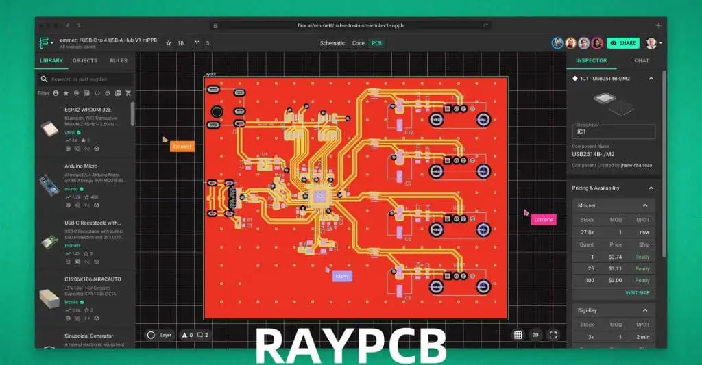
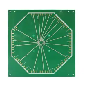
Analog circuits on printed circuit boards (PCBs) represent one of the most challenging and critical aspects of electronic design. Unlike digital circuits that deal with discrete logic states, analog circuits process continuous signals where every millivolt, microampere, and nanosecond can significantly impact performance. The transition from breadboard prototypes to production PCBs often reveals the harsh realities of parasitic effects, noise coupling, and thermal considerations that can make or break an analog design.

Fundamental Considerations for Analog PCB Design
The foundation of successful analog PCB design begins with understanding that the PCB itself becomes an integral part of the circuit. Every trace acts as a transmission line with characteristic impedance, every via introduces inductance, and every copper pour can create unwanted capacitive coupling. These parasitic elements, often negligible in digital designs, can dominate the behavior of sensitive analog circuits.
Ground plane design represents perhaps the most critical aspect of analog PCB layout. A solid, unbroken ground plane provides the reference point for all analog signals and serves as the return path for currents. However, the concept of “ground” becomes complex in mixed-signal designs where digital switching currents can inject noise into sensitive analog references. The solution often involves careful ground plane partitioning, where analog and digital sections maintain separate ground regions connected at a single point, typically near the power supply input.
Power supply distribution requires equally careful consideration. Analog circuits are notoriously sensitive to power supply noise, which can couple directly into signal paths through parasitic capacitances and shared impedances. Multiple bypass capacitors of different values create a distributed filter network, with small ceramic capacitors handling high-frequency noise and larger electrolytic or tantalum capacitors providing low-frequency filtering. The placement of these capacitors becomes crucial, with high-frequency bypass capacitors positioned as close as possible to sensitive analog components.
Signal Routing and Trace Management

Analog signal routing demands a fundamentally different approach compared to digital traces. Signal integrity depends not just on getting the signal from point A to point B, but on maintaining the signal’s analog characteristics throughout the journey. Trace impedance control becomes critical for high-frequency analog signals, requiring careful attention to trace width, dielectric thickness, and ground plane proximity.
Differential signaling offers significant advantages in analog designs by providing common-mode noise rejection. Differential pairs must maintain consistent spacing and equal length to preserve their common-mode rejection capabilities. Any mismatch in trace lengths or impedances can convert common-mode noise into differential-mode signals, degrading the circuit’s performance.
Crosstalk between adjacent traces represents another significant concern in analog designs. The coupling between parallel traces can introduce unwanted signals, particularly problematic when high-level signals run parallel to sensitive inputs. Adequate spacing, ground guard traces, and orthogonal routing on adjacent layers help minimize these interactions.
Component Placement Strategies
Strategic component placement forms the backbone of successful analog PCB design. The physical arrangement of components directly impacts signal paths, parasitic effects, and thermal management. Critical analog components should be positioned to minimize trace lengths while maintaining isolation from noise sources.
Op-amp circuits require particular attention to feedback path routing. The feedback trace should be kept as short as possible and positioned away from the input traces to prevent oscillation. Input matching networks for differential amplifiers benefit from symmetric layouts that maintain equal parasitic capacitances and inductances for both inputs.
Temperature-sensitive components like precision voltage references and analog-to-digital converters require careful thermal management. Positioning these components away from heat-generating elements like power regulators and providing adequate copper area for heat dissipation helps maintain performance across temperature variations.
Noise Management and Shielding
Noise in analog PCB comes from numerous sources: switching power supplies, digital clock signals, external electromagnetic interference, and thermal noise from resistors. Effective noise management requires a multi-faceted approach addressing each potential source and coupling mechanism.
Electromagnetic compatibility (EMC) considerations become paramount in analog designs. Sensitive analog inputs can act as antennas, picking up radiated emissions from nearby digital circuits or external sources. Proper grounding, shielding, and filtering help mitigate these effects. Guard rings around sensitive analog sections provide electrostatic shielding, while careful routing keeps high-frequency digital signals away from analog sections.
Power supply filtering extends beyond simple bypass capacitors to include active filtering techniques. Linear regulators, despite their lower efficiency compared to switching regulators, often provide superior noise performance for sensitive analog circuits. When switching regulators must be used, careful attention to switching frequency selection, output filtering, and PCB layout helps minimize their impact on analog performance.
High-Frequency Analog Considerations
High-frequency analog circuits introduce additional complexities related to transmission line effects, skin effect losses, and parasitic reactances. At frequencies above 100 MHz, PCB traces must be treated as transmission lines with controlled impedance matching to prevent reflections and signal degradation.
Via transitions between layers introduce discontinuities that can cause reflections and losses at high frequencies. Minimizing the number of via transitions and using multiple vias in parallel can help reduce these effects. Ground vias should be placed near signal vias to provide low-impedance return paths.
The choice of PCB substrate material becomes critical for high-frequency applications. Standard FR-4 exhibits increasing loss tangent with frequency, making low-loss materials like Rogers or PTFE-based substrates necessary for demanding applications. These materials offer better electrical properties but require modified fabrication processes and increased costs.
Mixed-Signal Design Challenges

Modern electronic systems increasingly combine analog and digital functions on the same PCB, creating unique challenges in managing the interaction between these domains. Digital switching creates current spikes that can couple into analog circuits through shared power supplies, ground planes, and electromagnetic fields.
Clock signal management becomes critical in mixed-signal designs. High-speed digital clocks can radiate significant electromagnetic energy that couples into sensitive analog inputs. Proper clock routing with adequate ground shielding, using differential clocking where possible, and minimizing clock signal edge rates help reduce this interference.
Analog-to-digital converters (ADCs) and digital-to-analog converters (DACs) represent the interface between analog and digital domains. These components require careful attention to both analog and digital design principles. Separate analog and digital power supplies, proper grounding techniques, and isolation between analog and digital sections help maintain performance.
Testing and Validation Considerations
Analog PCB designs require comprehensive testing and validation to ensure performance meets specifications across all operating conditions. Test point placement during the design phase enables efficient debugging and characterization. Critical analog nodes should have accessible test points while maintaining signal integrity.
Thermal testing becomes particularly important for precision analog circuits where temperature coefficients can significantly impact performance. Understanding how component values drift with temperature and designing appropriate compensation helps maintain accuracy across the operating temperature range.
Manufacturing and Assembly Considerations
The manufacturing process itself can impact analog circuit performance. PCB fabrication tolerances affect trace impedances and component placement accuracy. Assembly processes introduce thermal stress that can shift component values, particularly affecting precision resistors and capacitors.
Solder joint quality becomes critical for high-frequency analog circuits where even small discontinuities can cause reflections and losses. Proper solder mask design and assembly procedures help ensure reliable connections.
Future Trends and Emerging Technologies
The evolution of analog PCB design continues with advancing technologies and changing requirements. Higher integration levels push more analog functionality into specialized integrated circuits, reducing discrete component count but increasing the importance of power supply design and thermal management.
Advanced PCB materials continue to emerge, offering better electrical properties and thermal performance. Embedded component technologies allow passive components to be integrated directly into the PCB substrate, reducing parasitic effects and improving performance.
The increasing prevalence of high-speed digital interfaces requires analog designers to consider signal integrity effects that were previously confined to digital design domains. Understanding transmission line theory, impedance matching, and electromagnetic compatibility becomes essential for modern analog designers.
In conclusion, successful analog PCB design requires a deep understanding of the complex interactions between circuit topology, component placement, routing strategies, and manufacturing processes. The PCB becomes an active participant in circuit performance rather than simply a mechanical support structure. As electronic systems continue to demand higher performance, lower noise, and smaller form factors, the importance of masterful analog PCB design will only continue to grow.


