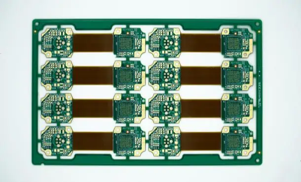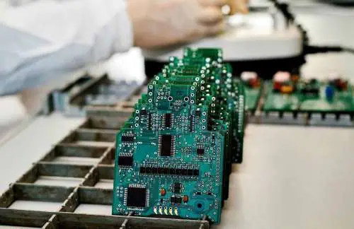
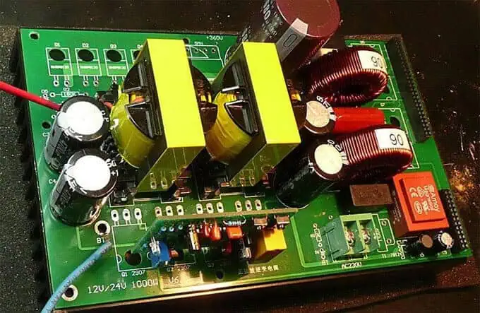
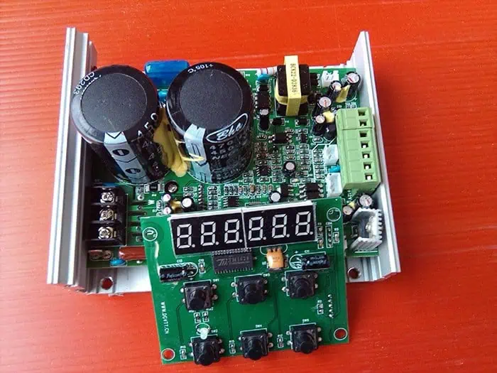
What is Frequency converter Circuit Board used for
A frequency changer or frequency converter is an electronic or electromechanical device that converts alternating current (AC) of one frequency to alternating current of another frequency. The device may also change the voltage, but if it does, that is incidental to its principal purpose.
How do Frequency converter device work ?
To increase the voltage, a DC to AC converter uses a electronic component called a step-up transformer. In a transformer, AC electricity flows through a coil of wire. .. The electricity from the second coil can then be used to power appliances.
Introduction
A power frequency converter (PFC) is an electronic circuit used to convert the input AC voltage to a DC voltage. It provides a stabilized DC bus voltage for the inverter stage in variable frequency drives and helps meet harmonic current requirements. Proper printed circuit board (PCB) design is crucial for optimal performance and reliability of the power frequency converter. This article provides key design tips and considerations for laying out the PFC circuit on a PCB.
PFC Topology Selection
The most common PFC topologies are:
- Passive PFC – Uses passive components like inductors and capacitors. Simple and low cost but has poor power factor and high harmonics.
- Active PFC – Uses active switches like MOSFETs or IGBTs. Provides high power factor and low harmonics. Commonly used topologies are:
- Boost PFC – Most widely used thanks to its high efficiency and power factor.
- Buck PFC – Good for applications requiring step-down voltage conversion.
- Bridgeless PFC – Eliminates bridge rectifier to reduce losses. Complex control.
Boost PFC is usually preferred due to its simplicity and performance. The PCB design guidelines covered in this article will focus on boost PFC.
Boost PFC Design Considerations
Following are some of the key factors to consider when designing a boost PFC PCB:
Input Filtering
An input EMI filter is required to attenuate high frequency noise and prevent conducted EMI. X capacitors, Y capacitors, common mode chokes, and line filters need to be properly selected. Careful component placement and routing techniques should be adopted to minimize EMI noise coupling. Keep traces short and use ground planes for shielding.
PFC Inductor
The boost inductor is one of the key components. It’s important to select the right inductor for the design requirements and lay it out properly on the PCB. Use thick copper tracks/planes for power connections to reduce losses. Minimize parasitic trace inductance by keeping traces short and wide. Provide sufficient clearances between the inductor and other components for cooling. Use via stitching around the pads for thermal relief.
Bus Capacitor
The PFC generates a high frequency ripple on the DC bus which must be filtered. A low ESR aluminum or film capacitor is required to minimize voltage ripple. Manage its location and orientation to facilitate cooling due to its heating. Provide sufficient capacitance based on requirements. Use multiple parallel capacitors if needed. Include fusing for safety.
Power Devices
The MOSFETs or IGBTs used must be properly rated for the design. Use Kelvin connections for the power terminals to avoid measurement inaccuracies. Provide proper gate drive design with low impedance traces. Include protection circuitry against transients. Use coplanar PCB pads for the devices with adequate thermal reliefs.
Sense Resistor
A current sense resistor is used for measuring inductor current. Select an appropriate high power, low drift, low tolerance resistor. Use a 4-terminal Kelvin connection for maximum accuracy. Manage its PCB location to minimize coupling noise.
Driver and Control Circuitry
The PFC controller and gate driver circuits require careful layout for signal integrity. Use proper grounding, decoupling capacitors, and isolation techniques. Route gate drive traces away from power traces to prevent coupling. Minimize trace lengths for fast switching response. Follow datasheet layout recommendations.
Thermal Management
The PFC circuit generates significant heat which must be dissipated properly. Use a multilayer PCB with sufficient copper thickness and thermal vias. Ensure unobstructed airflow over hot components. Provide adequate clearances around the heat generating parts. Use proper thermal interface materials. Include temperature monitoring circuity.
Key PCB Design Guidelines
Below are some key guidelines to follow when designing the PCB layout for a boost power factor correction circuit:
Separate Power and Signal Grounds
Have separate ground planes for power ground and signal ground to prevent coupling of noise. Connect the grounds properly at a single point. Power ground should use a large lower layer plane.
Optimize Component Placement
Strategically place components to minimize current loop lengths. Group associated circuits together. Position heat generating parts for better cooling. Ensure clearance requirements are met. Follow manufacturer guidelines.
Use Multilayer PCB
A 4-layer or 6-layer PCB with solid power and ground plane layers is highly recommended. This provides shielding, noise isolation and allows handling large currents.
Route Power Traces Carefully
Use adequate trace widths for current ratings. Avoid right angle turns. Minimize length of high current traces. Use 45° angles and arcs for traces carrying high di/dt currents to reduce EMI.
Provide Shielding
Use grounded copper planes and shields between noisy circuits and sensitive analog parts. Use shielding cans over critical high frequency circuits. Provide input EMI filtering.
Include Thermal Reliefs
Use thermal reliefs/spokes and vias under pads of heat generating components. This allows the heat to dissipate into inner board layers.
Follow DFM Guidelines
Design for manufacturability ensures the PCB can be easily and correctly fabricated. Use design rules for track spacing, via sizes, annular rings, etc.
By following these guidelines, a power factor correction circuit can be implemented on a PCB optimally for performance, cooling and reliability.
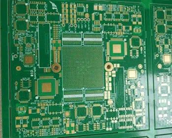
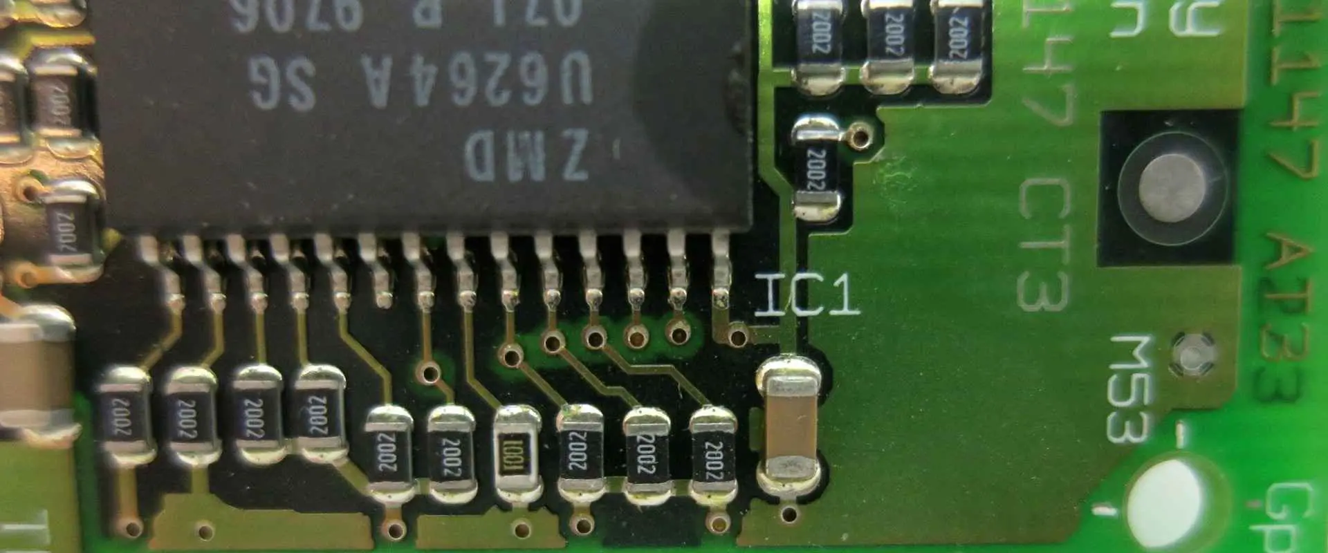
Example Boost PFC PCB Layout
Below is an example PCB layout for a boost power factor correction circuit with key components highlighted:
Figure 1. Example Boost PFC PCB Layout
Layout Details
- 4-layer PCB with complete ground plane layers for noise isolation
- Input bridge rectifier and filter capacitors placed close to the input terminal block for short leads
- Boost inductor placed close to the bridge output for short power loop
- Gate driver circuitry placed close to the MOSFETs to minimize trace lengths
- Bus capacitors distributed evenly near the MOSFETs
- Current sense resistors positioned near the inductor for accurate measurement
- Analog ground plane used under the control circuitry section
- Power ground fills the bottom layer under the power components
- EM fields contained with strategic slots in ground planes
- Shielding partition used between power and analog sections
This example demonstrates an effective layout for a boost PFC tailored for electrical and thermal performance. The techniques shown here should be applied when designing the PCB.
Conclusion

Designing a good quality PCB for a power factor correction circuit requires careful consideration of electrical parasitics, thermal management, EMI control and signal integrity. By using proper schematic design, component selection, and following the layout techniques described in this article, a high performance and reliable PFC can be realized. Some key takeaways are:
- Select appropriate PFC topology based on requirements
- Use quality PFC controller IC and optimized passive components
- Strategically place parts to minimize loop parasitics
- Provide sufficient cooling for heat generating parts
- Use 4-layer or 6-layer PCB with solid power/ground planes
- Route high current traces over ground plane using 45° angles
- Separate analog and power ground planes
- Incorporate shielding and noise control methods
- Follow datasheet recommendations and DFM guidelines
Using these PCB design best practices will lead to a power factor correction circuit with excellent electrical performance, thermal management, and noise immunity. This maximizes the reliability and efficiency of the complete power conversion system.
Frequently Asked Questions
What are some common issues seen with poor PFC PCB designs?
Some common issues with poor PFC PCB designs include:
- High trace inductance due to long power loops
- Poor cooling of heat generating components
- High EMI noise coupling due to lack of filtering
- Voltage spikes and transients due to uncontrolled di/dt
- Low efficiency due to high I^2R losses
- Unstable operation due to layout parasitic oscillations
- Inaccurate current/voltage sensing due to layout
How can the EMI from a PFC be minimized in the design?
To minimize EMI, use proper input line filters, enclose the PFC in a shielded metal enclosure, use grounded metal planes on the PCB, prevent gaps in ground planes using slots/stitching vias, route high di/dt traces over planes, use shield cans over noisy components, keep traces short, and follow good layout practices.
What PCB layers should be used for a boost PFC design?
A 4-layer board is usually adequate, with top and bottom layers for power components, signals, and connectors. The two inner layers should be assigned as ground and power plane layers for shielding and low impedance current flow. For complex designs, a 6 or more layer board can be used.
How can voltage spikes on the DC bus be reduced?
Voltage spikes can be minimized by using a snubber circuit across the power devices, minimizing loop inductance in bus wiring, using multiple decoupling capacitors near loads, slowing down dv/dt with inductive filtering, and using TVS diodes for clamping transients.
What design factors affect the efficiency of a PFC?
PFC efficiency is impacted by factors like proper choice of topology, devices, magnetics, optimum switching frequency, use of low loss components, minimizing parasitics, managing thermal dissipation, and good PCB layout. Every effort should be made to reduce I^2R losses in wiring and devices.
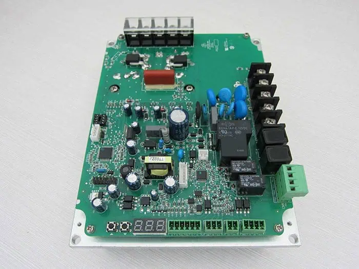
Basic circuit diagram analysis of the Frequency inverter
At present, most of the general-purpose Frequency inverters are AC-DC-AC inverters, usually the voltage converter is common, and its main circuit diagram (see Figure 1.1) is the core circuit of the inverter. (AC-DC exchange), DC filter circuit (energy-consuming circuit) and inverter circuit (straight-to-transform), of course, including finite current circuit, brake circuit, control circuit and other components.
1) Rectifier circuit
3) Inverter circuit
2) Filter circuit
1) Drive circuit
2) Protection circuit
3) Switching power supply circuit
4) Communication circuit on the main control board
5) External control circuit