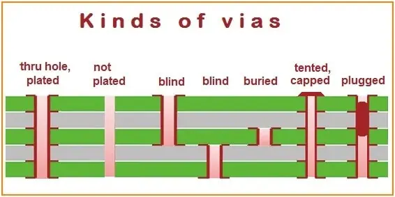
Vias serve as vital electrical interconnections between layers in a PCB stack-up. They create conductive pathways that allow components and traces to transmit signals across different board layers. Blind and buried vias enhance connectivity while minimizing the space required, making them particularly valuable in modern circuit design.
Various via types can be implemented in PCB manufacturing, each offering specific advantages for different design requirements. These specialized interconnections enable more complex and compact electronic designs by efficiently routing signals through the board’s structure.
Understanding Vias in PCB Design
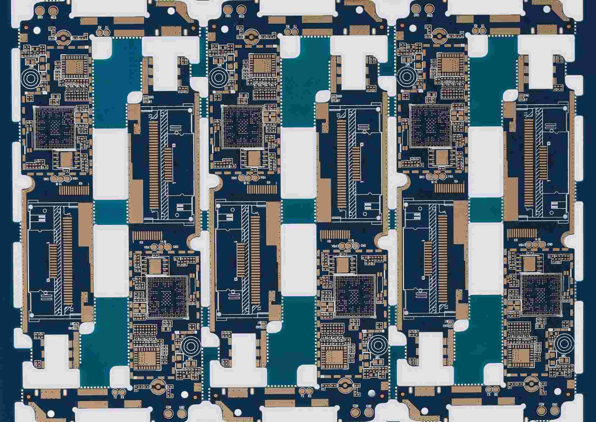
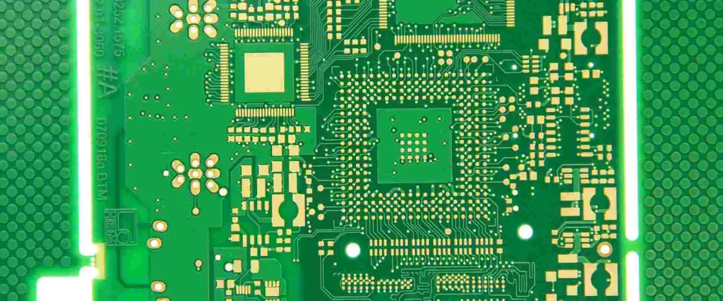
PCB Vias
Before we dive into the specifics of blind and buried vias, it’s essential to understand what vias are and their role in PCB design.
What are Vias?
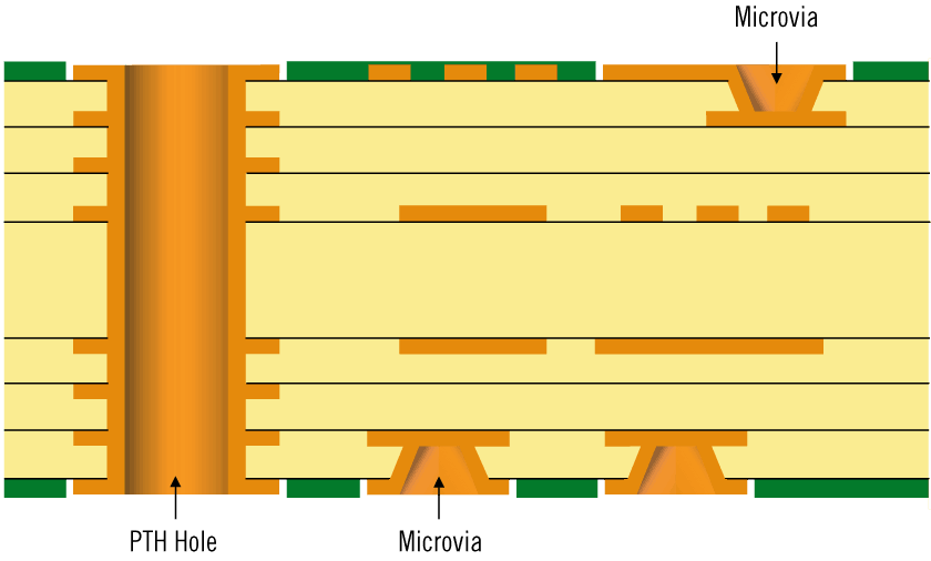
Vias are small holes drilled through a PCB that are plated with conductive material. They serve as electrical pathways between different layers of a multi-layer PCB, allowing signals to travel vertically through the board. Vias are crucial for creating complex circuit designs in a compact space.
Types of Vias
There are three main types of vias used in PCB design:
Blind Vias: Connecting the Surface to Inner Layers
Blind vias are one of the advanced via types used in modern PCB design. Let’s examine their characteristics, advantages, and applications.
What are Blind Vias?
Blind vias are holes that connect an outer layer (top or bottom) of a PCB to one or more inner layers, but not to the opposite outer layer. They are called “blind” because they are visible from only one side of the board.
Characteristics of Blind Vias
Depth: Typically extend through 1-3 layers
Visibility: Visible from one side of the PCB
Diameter: Generally smaller than through-hole vias
Fabrication: Require specialized drilling and plating processes
Advantages of Blind Vias
Space-saving: By not extending through the entire board, blind vias free up valuable real estate on inner and opposite outer layers.
Improved signal integrity: Shorter signal paths reduce signal degradation and electromagnetic interference.
Increased routing density: Allow for more traces on inner layers, enhancing design flexibility.
Better RF performance: Shorter vias have less inductance, improving high-frequency signal transmission.
Buried Vias: Hidden Connections Between Inner Layers
Buried vias offer another approach to increasing PCB density and complexity. Let’s explore their unique features and uses.
What are Buried Vias?
Buried vias are holes that connect two or more inner layers of a PCB but do not extend to either outer layer. As the name suggests, they are completely “buried” within the board.
Characteristics of Buried Vias
Location: Entirely within inner layers of the PCB
Visibility: Not visible from the outside of the board
Now that we’ve examined both blind and buried vias individually, let’s compare them directly to understand their relative strengths and weaknesses.
Design Flexibility
Both blind and buried vias offer increased design flexibility compared to traditional through-hole vias. However, they differ in how they provide this flexibility:
Blind vias excel in connecting surface-mount components to inner layers, making them ideal for designs with numerous surface components.
Buried vias shine in creating complex interconnections between inner layers, benefiting designs with intricate internal routing requirements.
Space Utilization
When it comes to maximizing PCB real estate:
Blind vias free up space on inner layers and the opposite outer layer.
Buried vias leave both outer layers completely available for component placement or routing.
Fabrication Complexity
The manufacturing processes for both types of vias are more complex than those for through-hole vias:
Blind vias require precise depth control during drilling and special plating techniques.
Buried vias necessitate sequential lamination processes, which can increase manufacturing time and cost.
Signal Integrity
Both via types can improve signal integrity compared to through-hole vias:
Blind vias offer shorter paths for signals traveling from outer to inner layers.
Buried vias provide optimal paths for signals traveling between inner layers.
Cost Considerations
Generally, both blind and buried vias increase PCB manufacturing costs:
Blind vias typically have lower fabrication costs compared to buried vias but may still be significantly more expensive than through-hole vias.
Buried vias often incur higher costs due to the complex sequential lamination process required.
Implementing Blind and Buried Vias in PCB Design
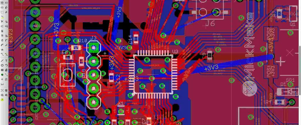
buried hole pcb
Successfully incorporating blind and buried vias into your PCB design requires careful planning and consideration. Here are some key factors to keep in mind:
Design Rules and Constraints
When working with blind and buried vias, it’s crucial to adhere to specific design rules:
Aspect ratio: The ratio of via depth to diameter should typically not exceed 8:1 for reliable plating.
Layer pairing: Plan which layers will be connected by blind or buried vias early in the design process.
Via stacking: Consider stacking vias to connect multiple layers while minimizing the number of drill operations.
CAD Tool Considerations
Modern PCB design software typically supports blind and buried vias, but designers should:
Ensure their CAD tool can accurately represent and validate designs with these via types.
Use layer stack managers to define and manage complex layer structures.
Utilize design rule checks (DRC) specific to blind and buried vias.
Manufacturability Considerations
To ensure your design can be reliably manufactured:
Consult with your PCB fabricator early in the design process to understand their capabilities and limitations.
Consider the impact on yield and cost when deciding between blind and buried vias.
Be aware of minimum via sizes and maximum depths that can be reliably produced.
The Future of Blind and Buried Vias
As electronic devices continue to shrink while increasing in complexity, the use of blind and buried vias is likely to become more prevalent. Several trends and developments are shaping the future of these advanced via types:
Miniaturization
The ongoing drive towards smaller, more powerful devices will push the limits of via technology:
Expect to see even smaller diameter blind and buried vias.
Higher aspect ratios may become possible with advances in drilling and plating technologies.
Enhanced Materials
New PCB substrate and plating materials may improve the performance and reliability of blind and buried vias:
High-frequency laminates optimized for blind and buried vias in RF applications.
Advanced plating materials to improve conductivity and reliability in high-aspect-ratio vias.
Automated via placement and optimization for blind and buried vias.
AI-driven design rule checking and signal integrity analysis.
3D Printed Electronics
As 3D printing technology advances, it may offer new possibilities for creating blind and buried vias:
Additive manufacturing of PCBs with integrated blind and buried vias.
Potential for more complex three-dimensional interconnect structures.
Conclusion: Choosing Between Blind and Buried Vias
The choice between blind vias, buried vias, or a combination of both depends on various factors specific to your PCB design requirements. Here are some key takeaways to guide your decision:
Use blind vias when you need to connect surface components to inner layers while maximizing inner layer space.
Opt for buried vias when you require complex inner layer connections and want to keep both outer layers free for components or routing.
Consider a combination of both types for maximum design flexibility in high-density, complex PCBs.
Always balance the benefits of these advanced via types against the increased manufacturing complexity and cost.
In conclusion, both blind vias and buried vias offer powerful solutions for increasing PCB density and performance. By understanding their characteristics, advantages, and applications, PCB designers can make informed decisions to create more efficient, compact, and high-performing electronic devices. As technology continues to advance, mastering the use of blind and buried vias will become increasingly important for staying at the forefront of electronic design.
A series circuit is a type of electrical circuit in which the components are connected end-to-end in a single loop. The same current flows through each element in a series circuit, but the voltage drops across each component can be different. Understanding series circuits is fundamental for analyzing DC and AC networks. This article provides an in-depth overview of series circuit fundamentals, analysis methods, characteristics, applications, and related concepts.
Series Circuit Basics
A basic series circuit consists of a voltage source, like a battery, connected to two or more electrical elements like resistors, inductors, capacitors, etc. The elements are chained together with wires in a single path for current flow.
Simple series circuit with battery and three resistors
Some key properties of ideal series circuits:
Single loop – Only one path for current to flow around the circuit.
Same current – The current is the same at every point due to single path configuration.
Voltage divider – Total voltage equals the sum of the individual voltage drops.
Series resistance – Total resistance is the sum of individual resistances.
Power distribution – Total power from source is distributed across each element.
These concepts allow systematic analysis of series circuits using basic circuit theory principles.
Several important methods are used to analyze series circuits:
Kirchhoff’s Voltage Law (KVL)
This fundamental law states that the algebraic sum of all voltages in a loop must equal zero. This is applied to find unknown voltage drops:
Copy code
Vs = V1 + V2 + V3 + ... + Vn
Where Vs is the total source voltage and V1 to Vn are the individual voltage drops across each element.
For example, in a circuit with a 45V battery and three resistors with voltages V1, V2, and V3, KVL gives:
Copy code
45V = V1 + V2 + V3
If two of the voltages are known, the third can be found by subtracting the known values from the total.
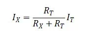
Voltage Divider Rule
The voltage divider rule is a short-cut method to determine the voltage across an individual element using its resistance relative to the total series resistance:
Copy code
Vx = (Vx/RT) * Vs
Where Vx is the voltage across element X, RT is the total series resistance, and Vs is the source voltage.
For example, if R2 is 220Ω, and the total series resistance is 1500Ω, with a 120V source, the voltage across R2 is:
Copy code
V2 = (220/1500) * 120V = 18V
This avoids having to find every intermediate voltage drop.
Current Calculation
For an ideal series circuit, the current is the same through every element, and can be found from Ohm’s Law:
Copy code
I = Vs / Rt
Where I is the constant current in Amps, Vs is the source voltage, and Rt is the total resistance from adding all individual resistances.
Power Ratings
The power dissipated in each element is calculated as:
Copy code
P = I2 * R
Where P is power in Watts, I is the series current, and R is the element’s resistance.
The total power dissipated is the sum of the individual powers.
Characteristics of Series Circuits
Beyond the basic principles, series circuits exhibit some key characteristics:
Current is Constant Everywhere
Due to the single path configuration, current cannot vary within a series circuit. Each passive component must have the same current flowing through it. This makes analysis using a single loop current straightforward.
Voltage Divider Effect
The total source voltage is divided up across each element proportional to its resistance, according to the voltage divider rule. Elements with lower resistance have larger voltage drops than high resistance components.
Resistance Adds in Series
For the overall circuit, series resistances simply add together. This holds true even for nonlinear devices like diodes or lamps, when their incremental resistances are added.
Impedances Add in General Series Connections
When reactive elements like inductors or capacitors are connected in series, their impedances add together rather than just resistances. For example, three impedances Z1, Z2 and Z3 in series have a total impedance of:
Copy code
Ztotal = Z1 + Z2 + Z3
Current Leads Voltage in Inductive Series Circuits
In a series L-R circuit, the current leads the voltage across the inductor due to its reactance. The opposite happens with a series C-R circuit, where current lags voltage.
Parallel Resistances Concept
Any branch resistance in parallel can be reduced to an equivalent series resistance using:
Copy code
Rseries = (R1*R2)/(R1+R2)
This allows simplification of branches to a single equivalent resistor.
Again, methodical analysis using series concepts matches the expected results.
Advanced Series Circuit Analysis
More complex scenarios involve combined resistance and reactance, or nonlinear elements like diodes:
Series RLC Circuit
Analysis involves vector addition of complex impedances
Impedances must consider both resistive and reactive parts
Allows determining overall circuit resonance and current
Series Diode Circuit
Must consider diode IV curve and nonlinear resistance
Resistance changes with current flow due to diode conduction voltage
Allows analyzing diode biasing and turn-on based on series resistance
These advanced tools enable thoroughly analyzing complex series circuits with diverse elements.
Common Applications of Series Circuits
Some typical applications that leverage series circuits:
Voltage Dividers
One of the most common uses of series connections is for creating voltage dividers. For example, measuring a high voltage using two resistors in series, where the lower resistor converts the high voltage into a lower measurable value.
Current Limiting
A resistor or inductor in series can purposely limit the current in part of a circuit. This protects components from excessive currents.
Impedance Matching
Inserting series inductors or capacitors allows matching the impedance looking into a circuit to the desired source/load impedance for maximum power transfer and efficiency.
Voltage Regulation
A series linear regulator uses a voltage sensing resistive divider combined with a series pass transistor to maintain a steady DC output voltage even with variations in supply voltage or load current.
EMI Filtering
Series inductors and capacitors can filter out electromagnetic interference by blocking high frequency noise while allowing lower frequency signals to pass through.
Signal Coupling
A series capacitor can couple AC signals from one stage to another while blocking DC voltages, allowing simple isolation of AC amplified signals.
If a break occurs in a series circuit, it becomes an open with no current flow. This is equivalent to a series element with infinite resistance blocking current.
Short Circuit
When two nodes in a series circuit contact each other, a “short circuit” occurs that bypasses part of the series loop. This often leads to excessive currents and is to be avoided in most cases.
Parallel Circuits
In contrast to series, parallel circuits provide multiple paths for current flow. Complex networks combine series and parallel connections, which are analyzed with techniques like nodal analysis or mesh current methods.
Series-Parallel Circuits
Some circuits contain both series and parallel combinations within an overall network. These compound connections can be reduced to simplified series-parallel equivalents for analysis.
Series Resonance
In series RLC circuits, resonance occurs when the total series impedance is minimized at the resonant frequency. This creates a bandpass filter effect around this frequency.
Series DC Motors
DC motors have the field and armature windings connected in series. This results in high starting torque since the initial current is limited only by the total resistance.
Conclusion
In summary, series circuits provide a fundamental topology for analyzing electric networks and understanding key concepts including current, voltage division, resistance addition, and load power distribution. While ideal series connections represent the basics, practical circuits require considering complex impedances, nonlinearities, and combined series-parallel networks. Facility with series circuit techniques forms the foundation for more advanced circuit analysis and design for electronics and power systems.
Frequently Asked Questions
What are the main characteristics of an ideal series circuit?
The key characteristics are: single loop topology, same current throughout, total voltage divides across elements, total resistance is the sum of individual resistances, and total power from source distributes among the components.
Why is current constant at every point in a series circuit?
Due to the single path configuration, charge carriers have no alternative route to flow so the current cannot change within a series circuit. Each element must pass the same current in steady state.
What happens if one resistor opens in a series circuit?
If one resistor opens, creating infinite resistance, current flow would stop. An open resistor is equivalent to disconnecting that part of the loop, so the circuit becomes open and voltage drops across the remaining components go to zero.
How do you calculate total resistance in a series circuit?
The total resistance is simply the arithmetic sum of the individual resistances. This holds true for any passive linear resistive elements. For nonlinear components, incremental resistances must be summed at the operating point.
Why is voltage division important in series circuits?
The voltage divider effect allows finding voltages across individual components from their resistances and the total voltage. This avoids tediously finding voltage drops across each preceding resistor to determine the voltage across a specific element.
The electronic circuits are made of PCB, components connected to each other in a meaningful way to function as per the design specifications.
These connections between the components is achieved by wiring or by PCB tracks. For a circuit prototype on Vero Board, the multiple and single strand wires are commonly used and soldered with electronic components in through hole package to form electrical connection. PCBs do use soldering of through and SMT type components by means of pads, vias and holes. However the breadboard do not require soldering because of all ready built in electrical tracks inside.
A soldering is the process of creating an electrical joint between components by melting the solder wire through applying heat and pouring that melted solder wire on leads/terminals of component to make a joint.
A soldering iron is device that is electrical 220/110V operated and is like pen and its tip/end is made of heating element. The soldering iron works simply. Plug into AC220V/110V outlet and starts to heat up. When you feel the heat and smoke starts then apply solder wire to “Tin” the tip.
Tinning:
Tinning the solder iron tip is also good, it helps the iron to grasp the solder quickly.
The tinning of copper wire is made so that the copper wire catches the solder and it will not break or bend and have the ability to create good electrical joint.
The solder sucker is used in “De-Soldering” process. When removing components from PCB or removing any leg/terminal of component from PCB then the solder sucker will remove the solder and relieves the component to pull out of PCB. Be careful while using solder sucker because some low quality PCB hole pads are weak and can breakout due to high vacuum of sucker thus rendering the hole useless.
The tweezer can be used as a tool to remove components from Vero board or PCB.
Solder Wire:
There are many types of solder available in market. The solder that is lead free, is a combination of tin 96.3%, copper 0.7% and silver 3% is a good option. Gauge # 21 is 0.032″ dia. The best melting point temperature for this type is 217OC – 221OC.
Solder Flux:
The flux is very important in soldering process. It reduces the oxidation and used to chemically clean the metal surface joint before and during soldering. The flux used in electronic circuits soldering is basically rosin flux or ammonium chloride. The flux helps enhance the soldering and “wetting” process. Flux prevent the formation solder balls by dissolving the oxide from metal joint surface.
Wetting is the adhesive force between the molten solder and solid copper wire that causes the molten solder drop to spread-out across the surface to form strong electrical joint. Cohesive force on the other hand causes the formation of solder balls and hinders the contact with metal/copper surface.
Soldering Station:
The temperature of soldering iron can be controlled by means of a “Regulator” which has the internal regulatory electronic printed circuit board to control the amount of current flowing through heating element. This is possible only in “Soldering Stations”. There are numerous soldering stations manufactures like Weller QB, and others. The have the “Control Knob”, “Toggle Switch”, “Temperature Display Unit” on the front panel and is operated by AC 220/110 V.
The solder stand is the place where you can put your iron at rest when not in use.
Soldering Gun:
The soldering gun is actually gun shape tool used for soldering purpose. It has a trigger when pressed to initiate soldering and when released to stop.
It is normally very difficult to handle wires that are being soldered. So there are clamp stands having crocodile clips to hold the wire. They also have PCB holding vise to ease soldering.
Wet cloth for cleaning iron tip
This is very important. It is the wet sponge or cloth to clean the iron tip regularly.
Soldering Tips.
Use the thinnest, 60/40 solder wire if you are a beginner
Select the appropriate size of solder iron tip. The thinner the tip the lesser the wattage and vice versa. 12Watt, 40Watt and 60 Watt irons have different applications. For precise SMT soldering use thinner tip and for THT use large tip iron.
Typical solder iron tip temperature is 330OC to 350O Allow iron to achieve this temperature. If iron do not attain this temperature then the cold solder joint will result. The cold solder joint is due to insufficient heat or movement of joint when cooling.
Keeping the iron ON will damage the soldering iron tip. Turn it off when not in use.
The plastic or wooden body side of solder iron is for holding. This is the cool side and hold it by your hand.
Touch the iron to the connection/joint/lead first, then apply solder and spread it. Look out for the drenched solder.
Too much solder is not useful. Appropriate solder is sufficient for good joint.
Do Tinning before making joint/connection
On regular basis check your soldering iron tip for any oxidation or residual flux. This hinders the soldering process. Try to clean it using wet sponge.
While cooling the solder joint, do not move.
Practice on scrap boards before working on actual board
Select the place of soldering where there is proper air ventilation.
Wear mask to avoid hazardous solder smoke
Be calm while soldering. Try not to shiver your hand while soldering.
Temperature Sensitive Components: Some of the components are sensitive to heat and high temperature, applying iron for longer time will damage the components. So to avoid thermal shock or high temperature, proper heat sinks in form of sheet metal clips may be clamped to dissipate the excessive heat away from PCB and components.
Solder Bridge: The solder bridge can form due to insufficient amount of solder mask on PCB. The solder bridge is the connection between the two points on PCB that were not meant to be connected. This solder bridge is formed accidently during soldering PCB components because of inappropriate solder mask
The deployment of 5G networks requires new spectrum bands to support increased data rates and connectivity. One of the key frequency bands being utilized for 5G is the 28GHz millimeter wave (mmW) band. This high frequency range allows for multi-gigabit data speeds, but also presents design challenges particularly related to radio components like filters and antennas. This article provides an overview of 28GHz mmW filters and antennas for 5G networks.
28GHz mmW Band Overview
The 28GHz band, from 27.5-28.35GHz, is being used for 5G deployments worldwide. Some key advantages of 28GHz:
Large amount of spectrum available – up to 850MHz depending on the region
High bandwidth channels to support multi-Gbps data rates
High frequency allows antenna arrays for beamforming and spatial multiplexing
However, the higher frequency also results in increased path loss and sensitivity to blockages. Omnidirectional coverage is difficult, so highly directional beamforming antennas are required. The small wavelength also leads to more challenging filter and antenna designs.
Spectrum Allocations
The 28GHz band plan varies regionally:
North America: 27.5-28.35GHz (850 MHz)
Europe: 24.25-27.5GHz (3.25 GHz)
Asia: 26.5-29.5GHz (3 GHz)
The amount of spectrum directly impacts the maximum data rate per user or cell, making the North American allocation most attractive for operators.
Propagation Characteristics
Due to the high frequency, 28GHz signals experience higher free space path loss and atmospheric absorption compared to sub-6GHz 5G bands. The Small wavelength also leads to diffraction loss around obstructions.
Typical path loss exponents range from 2.5 to over 4 depending on the environment. Signals can be blocked by buildings, foliage, human bodies, etc.
This leads to shorter communication range, on the order of a few hundred meters cell radius in urban areas. More cell sites are required to maintain coverage compared to lower frequencies.
Beamforming and MIMO
To compensate for the reduced range, 28GHz systems utilize beamforming and MIMO antenna arrays. Highly directional beams between the user and base station maintain link budget. Phased array antennas allow rapid beam steering and tracking.
MIMO techniques like spatial multiplexing are employed to increase data capacity using multiple streams. The small wavelength allows dozens of antenna elements to be integrated into a compact array. 5G specifications target up to 256-element arrays for mmW systems.
Filters play a critical role in the 28GHz radio front end to reject out of band interference and noise. The small wavelength places strict demands on filter performance and technology.
Insertion Loss
Minimum insertion loss is critical to maintain link budget. Each 1dB of loss cuts the effective communication range. Target specifications are 2dB or less over the passband.
Bandwidth
The filter must have sufficient bandwidth to pass the full 28GHz spectrum allocation, up to 850MHz for North America 5G bands. Minimum fractional bandwidth is >3%.
Rejection
Strong rejection of adjacent frequency bands is needed to avoid interference and blockers. >30dB rejection should be maintained within 100MHz of band edges. >50dB rejection further away.
Power Handling
Transmitted power is limited for 28GHz, but filters must handle at least 30dBm transmit power levels without distortion. Higher power handling reduces insertion loss.
Size
Extremely compact size is required to integrate filters into the RF front end. Surface mount packaging with <5mm footprint is typical. Size is driven by manufacturability.
Cost
Low cost is needed for wide adoption in mmW products and infrastructure. Simple architectures with easy manufacturing are preferred. Tuning and adjustment must be minimal.
28GHz Filter Technologies
Many filter technologies have been researched and developed for 28GHz applications:
LC Resonator Filters
Advancements in MEMS and lithography enable miniaturized LC filters up to 30GHz
Low loss, moderate rejection, compact size
Parallel plate/overlay capacitors and spiral inductors are commonly used
Bandwidth control can be challenging
Cavity Filters
Waveguide or dielectric resonator cavities for high Q, low loss
LC filters provide the best combination of low loss and wide bandwidth but require advanced MEMS or semiconductor fabrication.
SAW and BAW suitable for low cost, moderate performance filters up to 30GHz. Limitations on loss and bandwidth.
Cavity and acoustic waveguide filters for high performance, but higher cost and larger sizes.
5G 28GHz Antenna Requirements
Like filters, antennas operating at 28GHz mmW face stringent demands for 5G performance. Key parameters include:
Gain
High gain is essential to counter path loss and close the link budget. Required EIRP reaches up to 55dBm with base station antenna gains over 30dBi.
Beam Steering
Electrically steered directional beams for capacity and range. Wide azimuth and elevation scanning range supports beamforming and spatial multiplexing.
Bandwidth
Antenna bandwidth must cover the full 28GHz band up to 850MHz. Impedance matching required over the band. Gain variation < 3dB.
Efficiency
Minimize loss mechanisms like conductor and dielectric loss. 70%+ radiation efficiency needed to support high EIRP levels.
Size and Weight
Compact size and low weight desired to enable dense deployments on poles, rooftops, etc. Size under 8″ diameter x 4″ depth typically required.
Reliability
Robustness for outdoor operation in harsh environments. Stable performance over temperature and humidity extremes.
Cost
Making 5G mmW deployments commercially viable requires low cost antenna arrays and components, without sacrificing performance.
Similar to filters, meeting these specs requires advanced antenna technologies and architectures:
Substrate Integrated Waveguide (SIW) Arrays
Low loss propagation in integrated waveguide form
Beam scanning via frequency tuning or phased array
Moderate bandwidth, gain up to ~25dBi
Integration with PCB and semiconductor manufacturing
Microstrip Patch Arrays
Low profile, lightweight, low cost
Gain up to 30dBi with 1000+ elements
Limited scan range and bandwidth
Dielectric and conductor losses increase with frequency
Reflectarrays/Transmitarrays
Parabolic reflector performance made planar
Extremely high gain and efficiency
Steered beams with tunable phase shifters
Narrow bandwidth and limited scan range
Complex feed array required
Dielectric Resonator Arrays
Very low loss, high radiation efficiency
Moderate bandwidth and gain up to 28dBi
Complex feeds and power distribution
High Q resonance limits steering agility
Summary
Microstrip patches optimal for low cost phased arrays with moderate performance
SIW arrays combine high performance with easier manufacturing
Advanced architectures like reflect/transmit-arrays provide highest gain and beam control
MIMO and Multi-Beam Arrays
MIMO spatial multiplexing at 28GHz uses multi-beam antennas or arrays mounted in various orientations to provide diverse spatial channels for multiple data streams.
Typical configurations utilize:
4 to 16 antenna arrays per base station
Each array may have up to 256 dual-polarized antenna elements
Arrays distributed to provide 360 degree azimuth coverage
Antenna mounting directions optimized to maximize channel separation
Multi-beam arrays allow simultaneous transmission/reception with multiple UEs to increase capacity. Each array generates multiple fixed or steerable beams using sub-arrays with phase shifters or tuning elements.
The shift to 5G in mmW bands like 28GHz brings formidable challenges in designing radio components like filters and antennas. High performance, small size, and low cost need to be simultaneously achieved. A variety of filter and antenna architectures show promise in targeting the demanding requirements for 28GHz operation. Ongoing research and product development continue to optimize mmW components and arrays to make high frequency 5G commercially viable worldwide. Careful selection of filter and antenna technologies allows balancing performance, size, and cost.
Frequently Asked Questions
What is the main driver for using the 28GHz band in 5G?
The large amount of spectrum available in the 28GHz range, up to 850MHz in some regions, enables very high data rates up to multi-Gbps speeds per user. The wide bandwidths support high capacity 5G networks.
Why are highly directional antennas needed at 28GHz?
Due to the high free space path loss at such high frequencies, directional antennas with high gain are essential for closing the link budget and achieving reasonable range. Omnidirectional coverage is very difficult. Directional beamforming maintains signal strength.
How does beam steering work for 28GHz antennas?
Phased array antennas are commonly used for beam steering at 28GHz. By adjusting the phase of the signal at each antenna element, the beam direction can be electronically pointed without mechanically moving the antennas. This allows fast adaptation of the beams for capacity and coverage optimization.
What is a typical data rate achievable with 28GHz 5G?
Using advanced modulation up to 256QAM and large channel bandwidths allocated at 28GHz, data rates up to 2Gbps may be achievable with 28GHz NR. This supports applications like 4K/8K video streaming, mobile broadband, and fiber-like wireless connectivity.
Why is filter rejection important for 28GHz?
Strong out-of-band rejection is critical for 28GHz filters to avoid interference from adjacent frequency bands and blockers that could desensitize the receiver. The filter must provide high isolation from nearby spectrum to maintain sensitivity. 30dB rejection within 100MHz of the band edge is typical.
Have you ever experienced when you rub the comb on pull over, you can pick the small pieces of paper or when you rub the balloon, and it will stick to yourself. Another powerful example is the thunderbolt of lightning during heavy rainy season.
These all are the examples of static electricity.
What is Static Electricity..?
So what is static electricity actually..? The static electricity is basically the imbalance of charge produced by mechanical movement between two bodies’ surfaces.
One of the body is the bad conductor of charge called insulator when rubbed against a material surface it causes the resistance/friction that in turns creates “static charge”.
Actually all the matter exist in the universe is made of tiny particles called “atoms”. These atoms are further broken into 3 basic constituents called “electrons”, “protons” and “neutrons”. The matter is classified into elements in periodic table. There are 118 elements in periodic table till now. The atom is electrically neutral because of equal number of protons and electrons. The electrons are loosely bonded and can escape away the shell of atom upon small excitation energy or mechanical movement like friction.
The neutrons and protons are tightly bonded together in the nucleus of atom. The nucleus is the heaviest part of atom. The number of protons forms the identity of element. It is near impossible to extract / kick off proton from nucleus. Because if we can do this we could have changed the nature/identity of element. However neutron can be kicked off nucleus and as a side effect emits radioactive waves. Now when the electron from the valenceshell is removed or electron added into the valence shell then it will become positive charged or negative charged respectively.
Benjamin Franklin’s Experiments Observations:
The fluid model of static electricity, was discovered by early scientist and pioneer researcher named Benjamin Franklin. He witnessed that upon rubbing glass rod with silk cloth will cause force of attraction between the two.
When the wax was rubbed against wool cloth this will also cause force of attraction between the two.
It was also observed that if two glass rods were rubbed with their respective silk cloths then these two glass rods repel each other. Hence generating force of repulsion.
Another observation was that when glass interacted/rubbed with silk and wax interacted/rubbed with wool then wax and glass would attract one another.
Hence it is was speculated by Franklin that some sort of invisible “Fluid” is transferred between two bodies during the process of rubbing. This transfer of fluid would render one body positively charged and another negatively charged. This positively charged and negatively charged were related to the deficiency and excess of that “fluid”. This hypothetical transfer of fluid then become “Charge”.
Hence it is was postulated that charge that is created by rubbing wax was negative and that charge created by rubbing wool is positive.
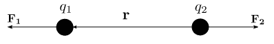
Charles Coulomb used the special device called “Torsional Balance” to measure exact value of charge. His experiment than came to following result
“If two point objects equally charged to 1 coulomb having no physical mass are placed at a distance of 1 meter apart, then there exist a force of 9 billion Newton either attractive force or repulsive force for opposite charges and similar charge types respectively. ”
The unit of measurement of charge was dedicated to the name of Scientist “Coulomb”.
1 Coulomb of charge is actually the excess or deficiency of electrons. Or conversely speaking 1 electron charge is equal to Coulomb (C)
Where F = Electrostatic Force
k = Coulomb’s Constant =
q1 and q2 are two point charges
r = distance between two point charges in meters
Static Electricity Phenomenon In terms of Electronic Charge:
When the two neutral bodies/materials are brought close together and rubbed with each other, this will create movement in electrons. The electrons will start to leave from one body and enter other body. The body that releases electrons is said to be positively charged due to scarcity of electrons and the body that receives electrons is said to be negatively charged due to excess of electrons.
Examples of Static Electricity:
Hat and Hair Example of Static Electricity:
In the context of all discussion above it is now clear that when we take off the hat our hairs stick to the hat because of transfer of charges/electrons from hair to hat. This will create negative (excess of electrons) static electricity on hat and positive (deficiency of electrons) static electricity on hair.
Static Electricity Balloon Example:
We can also say that a charged object will attract neutral object because of the same electrons flow from charged object to neutral. Example of this is a balloon that when rubbed on your hair will get negative charge, then it is brought near to the neutral wall but the balloon will stick to the wall because of electron flow from balloon to wall. This is also true for the case when we brush our hair with comb then the comb can pick up small pieces of paper.
The friction in the clouds in rainy season cause the generation of static electricity. This static electricity is stored in the clouds but is visible due to millions of volts created spark in sky. This static electricity converts into electrical current when some sort of current path is generated from clouds to the ground like a kite can bring the thunderbolt to the earth surface.
Ozone Cracking:
The ozone is created due to static discharge. This ozone is not good for elastomers. This ozone can make deep cracks in vehicle components like O-rings. The damaged fuel line from ozone can cause fire. To protect from this use elastomers that resist ozone.
Static Electricity vs Current:
The charged objects will hold these states of excess / scarce electrons until it is applied by external force to move it in a particular direction. These electromotive force (EMF) or “voltage applied across” will cause the electron to flow thus converting static electricity into “current”.
Currentis alwaysmoving in a direction through a metallic wire. While static electricity remain stored in a body when applied to mechanical friction/movement.
RoHS stands for Restriction of Hazardous Substances and is an important regulatory standard that impacts the electronics industry. RoHS compliance dictates restrictions on certain hazardous substances in electronic products and components. For printed circuit board (PCB) manufacturers, understanding and implementing RoHS compliance is crucial.
This guide will provide a comprehensive overview of RoHS, including:
RoHS directive history and timeline
Substances restricted under RoHS
RoHS scope and exemptions
Requirements for PCB manufacturing
How to demonstrate RoHS compliance
RoHS certification standards
Cost impact of RoHS compliance
Future outlook for RoHS
By the end of this article, you will have a deeper understanding of this critical set of regulations and how to ensure your PCB assembly process and supply chain upholds RoHS standards.
RoHS stands for “Restriction of Hazardous Substances” and originated as a European Union directive known as “Directive 2002/95/EC” adopted in February 2003. The original RoHS directive focused on restricting certain hazardous substances in electrical and electronic equipment (EEE).
The motivation was to address health and environmental concerns around substances like lead, mercury, cadmium and other heavy metals found in electronics. RoHS regulations mandated stricter limits on these substances with a combined threshold percentage limit of 0.1% by weight per homogeneous material in applicable EEE.
The current version of the RoHS Directive is referred to as “RoHS 2” or “RoHS Recast.” It was published as Directive 2011/65/EU which updated and recast the original legislation. RoHS 2 expanded the scope of products covered while keeping the restricted substances largely the same.
Some key dates in the history of RoHS adoption include:
February 2003 – Original RoHS Directive 2002/95/EC enters into force
July 2006 – RoHS 1 takes effect and EEE in EU market must comply
January 2009 – Commission exempts medical devices until 2014
January 2011 – Commission exempts monitoring equipment until 2014
July 2011 – RoHS 2 Directive 2011/65/EU is published
January 2012 – RoHS 2 enters into force
January 2013 – RoHS 2 compliance required
RoHS has gone through gradual expansion of its scope over the years since its inception while maintaining focused restrictions on some key hazardous substances.
Restricted Substances Under RoHS
The RoHS directives impose restrictions on the following main substances:
Lead (Pb)
Mercury (Hg)
Cadmium (Cd)
Hexavalent chromium (Cr6+)
Polybrominated biphenyls (PBB)
Polybrominated diphenyl ether (PBDE)
The maximum threshold level permissible for these restricted substances by weight in homogeneous materials is 0.1% (1000 ppm).
Additionally, RoHS 2 added four phthalates to the list of restricted substances:
Bis(2-ethylhexyl) phthalate (DEHP)
Butyl benzyl phthalate (BBP)
Dibutyl phthalate (DBP)
Diisobutyl phthalate (DIBP)
These hazardous substances were included in electronics primarily due to their properties in applications like lead solder, mercury switches, cadmium plating, and flame retardant plastics. However, the potential risks posed led to regulations limiting their use. Eliminating these from the supply chain required a major shift in materials and processes for the electronics industry.
RoHS Scope and Exemptions
RoHS 2 expanded the scope of applicable product categories versus RoHS 1. The legislation covers electronic equipment and devices that:
Rely on electric/electromagnetic fields for functioning
Generate, transmit, or measure such fields
Use voltage not exceeding 1,000 volts AC and 1,500 volts DC
Out of scope categories include military equipment, aerospace equipment, certain large-scale industrial tools, implantable medical devices, photovoltaic panels and some others.
Within the product categories covered under RoHS 2, the legislation allows for certain applications and materials to be exempt from the substance restrictions based on technical feasibility or reliability. Some current exemptions include lead in high melting temperature solders, lead in glass or ceramics, lead in server or storage system batteries, among others.
RoHS Requirements for PCB Manufacturing
Printed circuit board manufacturing and assembly is squarely within the scope of RoHS 2, since PCBs are core components of nearly all electronic equipment. This has major implications for PCB material sourcing, fabrication, assembly, and testing processes in order to comply. Here are key requirements for PCB manufacturing under RoHS:
Substrate and Laminate Materials
Base substrate materials like FR-4 must not contain brominated flame retardants like PBB or PBDE exceeding the 0.1% threshold
Prepreg bonding films also cannot contain these hazardous brominated compounds
Ceramic or composite substrates need to avoid restricted phthalates
Solder
Lead-free solder alloys like tin-silver-copper must be used instead of tin-lead solder
Solder flux also should not contain prohibited substances
Plating
Surface finishes need to eliminate hexavalent chromium and cadmium plating
Since RoHS regulations pertain to end products sold in the EU market, PCB manufacturers must be able to demonstrate RoHS compliance through documentation and traceability. Key ways to show compliance include:
Material Declarations
Suppliers of substances, materials like laminates must provide material declaration forms listing any restricted substances and their concentrations.
Certificates of Conformity
Certificate to declare RoHS compliance for the specific product being placed on EU market.
Test Reports
Independent lab testing reports to validate concentrations of restricted substances in materials or components are below permissible levels. This can involve analytical testing like GC/MS.
Markings
RoHS compliant labels, markings on PCBs and consumer end products. For example “RoHS” or “Lead-Free.”
Chain of Custody
Documentation tracking materials through the entire supply chain to prove compliance at every step.
Maintaining this documentation provides evidence of RoHS conformance during any audits or regulatory inquiries.
RoHS Certification Standards
To ease the burden of compliance demonstration, industry standards have been developed that allow manufacturers to certify their products or materials are RoHS compliant once criteria are met. Two common standards include IPC and UL certification programs.
IPC-1752 Class D Materials Certification
Standard published by IPC to certify materials as RoHS compliant with extensive testing requirements and stringent control levels.
Allows materials suppliers to produce independent certification.
Class 1-3 also exist for parts and components, PCBs, and electronics assemblies.
UL 1007 Standard
Published by Underwriters Laboratories (UL) as a standard for RoHS materials verification
Covers restricted materials testing methodology and acceptable concentration levels
UL issues certificates for complying materials as recognized proof of RoHS conformance.
By having materials or boards be certified through these standards, manufacturers have recognized means to demonstrate RoHS compliance to customers and regulatory authorities.
Cost Impact of RoHS Compliance
Transitioning to RoHS compliant materials, components and processes did involve some cost increases for electronics manufacturers:
Reformulation of laminates, prepregs, coatings to replace brominated FR additives
New plating processes like immersion silver instead of hexavalent chromium
More expensive solders like SAC alloys instead of tin-lead
Component costs increased from lead-free terminations, marking, compliance testing
New process controls around material handling, storage and traceability
Increased documentation, certification, and record-keeping overhead
However, over time these costs diminished as compliant materials and processes matured and economies of scale optimized RoHS implementation. Substitutes like halogen-free FR materials eventually reached cost parity with older materials. Solder costs also declined.
For PCB manufacturers, careful supplier management and process controls enabled cost-effective RoHS compliance. The regulation is now well-integrated into electronics manufacturing.
Future Outlook for RoHS
As awareness around sustainability grows, expectations are for the scope and stringency of RoHS regulations to expand further:
EU has stated intention to periodically review and add restricted substances to RoHS as needed.
Exemptions may also be phased out over time if technically feasible substitutes emerge. This pushes industry to develop innovative solutions.
More product categories and electronics could come under RoHS legislation as scope gaps get addressed.
Tighter control limits on maximum permissible concentrations are also possible.
Expect alignment and convergence between different global environmental regulations.
For PCB companies, retaining organizational agility and supply chain flexibility will be key to adapt to future RoHS changes. Staying abreast of emerging substitutes and sustainable materials will also allow companies to turn compliance into competitive advantage.
Conclusion
RoHS stands as one of the most influential environmental regulations shaping the electronics industry over the past two decades. Its restrictions on hazardous substances fundamentally changed materials, components and processes for PCB manufacturing.
While adapting to RoHS compliance did entail costs and process changes, manufacturers have largely integrated its ethos into operations. With proper material evaluation, process controls, certification and documentation, PCB assemblers can readily demonstrate RoHS conformance.
As the scope expands and companies focus more on sustainability, RoHS principles will continue guiding the industry’s responsible use of materials for benefit of human health and the environment.
Here are some common questions around RoHS compliance for PCB manufacturing:
Q: Does RoHS apply to PCB manufacturers outside the EU?
RoHS applies to any PCBs that will end up in products sold or imported into the EU market, irrespective of where they are manufactured. So PCB assemblers globally must comply if boards will reach EU countries.
Q: How are RoHS regulations enforced for non-compliant products?
Within the EU, enforcement is handled at the national member state level through market surveillance. Customs agents or regulators can do sample procurement and testing to check for compliance, issuing penalties for violations. They can also force recall and disposal of non-compliant products.
Q: Can any deviations be allowed from the maximum substance concentration limits under RoHS?
In general, RoHS takes a strict interpretation of the 0.1% threshold substance limit in materials. However, the IPC-1752 standard does permit maximum levels of up to 0.2% for cadmium and mercury to account for measurement uncertainties and trace contaminants. Still, the main limit remains 0.1%.
Q: Does RoHS restrict only substances intentionally added or even trace contaminants?
RoHS covers both intentionally added restricted substances as well as contaminants arising from production of the material that may exceed permissible thresholds. Manufacturers are responsible for limiting both.
Q: Can normal FR-4 laminates still be used in RoHS compliant PCBs?
Yes, as long as the FR-4 laminate meets RoHS requirements. Usually this means replacing the brominated compounds previously used for flame retardancy with polymeric or reactive phosphorous-based FR additives that are RoHS compliant. RoHS-compatible FR-4 laminates are widely available.
Q: Does RoHS compliance also require lead-free component soldering?
Yes, for an assembled PCB to be fully RoHS compliant it requires lead-free soldering. So components must have lead-free terminations and lead-free solder alloy like SAC305 must be used to solder components to the board. Lead-free solder process controls are part of overall RoHS conformance.
What is RoHS and Why is Important
In 2003, the European Union (EU) created a legislation to restrict the use of hazardous substances in Electronics and Electrical industry for the sake of environmental and people safety and health issues. This legislation itself is known as RoHS (Restriction of Hazardous Substance)
We know that electronics and electrical industries have soared too much. People are buying electronics at unimaginable pace, from smart phones, to IoT products, computers, laptops, house hold equipment, auto industry, Wire, cables, connectors, components are widely available in the market from lowest grade quality to highest grade quality.
The low quality component and devices are cheap and high quality is expensive. So people tend to buy cheaper electronics to fit in their budget constraints. However they do not realize the dangers associated with cheap quality electronics, components and devices. Low quality products means products using Non-RoHS electronic components/materials in them.
The one biggest problem of RoHS is nothing more than “Expensive Products”. Why would a company choose components/materials for manufacturing their product that are expensive (RoHS compliant)..?
These expensive components or materials used to manufacture product will surely increase the price of end product thus reducing the profit margin of the company. This is the reason why many EE companies opt for Non-RoHS components.
This is the same case with individuals whose TV set if have some problem, that individual will use lead solder (that is cheap) for de-solder or repair purpose because lead free solder is little bit expensive so as to save money but in return inhaling solder fumes which is deadly for lungs.
So the question is “Should we use materials (as an EE company and individual working as hobbyist or repairman) that comply with RoHS standards while realizing that the end product or cost of service will increase thus possibly declining profit and reducing market. The answer as per the EU standards (CE Mark) is YES..!
This is because RoHS standards were designed not considering the financials or monetary implications of any individual or a company but to ensure welfare of people in terms of health and cleaner environment
Dangers Associated with Non-RoHS Materials:
As mentioned that RoHS legislation standards are important because to make sure that environmental pollution is reduced and people health care issues are resolved. Imagine a company that has a PCB assembly and PCB manufacturing facility where materials that are Non-RoHS compliant are used. Now you can imagine that people who are engaged in daily routine work on a conveyer belt handling those materials will suffer from different diseases of skin and lungs cancer, mesothelioma and asbestosis.
Those labor which are packaging these Non-RoHS PCB materials and products will also suffer because they handle materials with their bare hands. Thus everyone involved in handling these stuff manufacturing labor, packager, supplier, distributor will not be affected immediately or shortly but will be affected in longer run surely.
The dangers associated with Non-RoHS products/materials is not just limited to manufacturing and handling but during and after use, they are discarded and become part of Landfills. Because of longer life cycle of these Non-RoHS materials they do not decay soon, but take very long time to degrade/decay. Thus when thrown away in landfills (holes in the ground), their traces are mixed in underground water resources hence polluting environment, plants and fishes.
Keeping in view above hazards, RoHS directives 2011/65/EU known as RoHS-2 was introduced in 2011 and directives 2015/863 known as RoHS-3 was introduced in 2015.
RoHS-2 directives 2011/65/EU introduced the restriction on the use of Bis (2-ethylhexyl) phthalate (DEHP) and Di-isobutyl phthalate (DIBP). The ROH-2 was specific for medical instruments for monitor and control and other EE equipment not covered. ROHS-2 also included the CE (Compliance Europe) Marking standard.
RoHS-3 added 4 new materials in the list of six Non-RoHS restricted materials under directive 2015/863. These are Bis (2-ethylhexyl) phthalate (DEHP), Butyl benzyl phthalate (BBP), Di-butyl phthalate (DBP) and Di-isobutyl phthalate (DIBP)
ELV Directive:
The End of Life Vehicle (ELV) is another directive of EU about the scrap cars and waste materials regarding wires, cables and electrical accessories. The ELV directive restricts the use of banned materials in the list given below in automobile industry.
WEEE Directive:
WEEE stands for Waste Electronic and Electrical Equipment. The Collection, treatment and recycling of waste electronics is the mandate of WEEE directive. It urges the electronic and electrical product manufacturers to comply with this standard otherwise legal action will be taken against those who do not comply in terms of thousands of dollar fine.
On the other side, awareness of WEEE and RoHS needs to be spread. The EE product designers and manufacturers need to make products such that they facilitates extraction of useful components and materials like silver, gold, platinum, copper, aluminum, during recycling process.
RoHS Restricted Materials:
The RoHS standards have defined the admissible (minimum) amount of restricted materials that can be used in a product. This amount is measured in Parts per Million (ppm). So 1 ppm means out of every 1 million parts of RoHS compliant material, only 1 part of RoHS non compliant material is allowed.
The list of total 10 restricted materials along with their ppm (RoHS non compliant) is given below
If you are still using one of the RoHS non complaint substances listed above and you are anywhere outside Europe then it is fine, but if you are in Europe then you may have to face consequences in terms of heavy penalty or even imprisonment. Any EE product that is sold in Europe it MUST be RoHS complaint and CE certified.
Eagle (Easily Applicable Graphical Layout Editor) is a popular printed circuit board (PCB) design software developed by CadSoft and now owned by Autodesk . It allows electronic engineers and hobbyists to easily design schematics and PCB layouts for various electronic devices and circuits .
Some key features of Eagle include :
Schematic capture editor for creating circuit schematics
With Eagle, you can take a circuit idea from schematic design to PCB ready for fabrication. Its easy-to-use interface and powerful features make Eagle a great choice for hobbyists, students, and engineers alike .
In this comprehensive guide, we will cover everything you need to know about using Eagle PCB software .
While transitioning from schematics to PCB layout in Eagle, keeping some best practices in mind will ensure your design goes smoothly :
Maintain proper clearance between traces based on voltage levels
Keep high voltage traces short and provide enough isolation
Route clock signals before other traces for signal integrity
Avoid right angle or acute angle traces, use 45° angles when possible
Use ground and power planes on inner layers for noise isolation
Distribute bypass/decoupling capacitors evenly over the board
Keep matched length for traces like differential pairs and clock signals
Minimize trace length variations between related signals
Plan component placement to minimize track lengths
Verify design rules like width, spacing, mask etc. before manufacturing
Proper PCB layout techniques will ensure your design performs as expected when manufactured. Eagle gives you all the tools to implement these best practices.
Downloading Components and Libraries
Eagle comes bundled with a large selection of ready-made components and symbols. However, you will often need additional specialized parts for your designs . Here are some ways to obtain new libraries and footprints :
Check Eagle’s default libraries for missing part numbers
Manufacturer websites often provide Eagle libraries
GitHub has many user-submitted Eagle libraries
Use Eagle library editor to create custom components
Check community forums like Eagle element14 for part requests
Contact the manufacturer directly for official models
Consider using generic substitute parts for prototyping
With access to additional libraries, you can design using all the parts required for your project!
Tips for Working Faster in Eagle
Like any software tool, there is a learning curve to using Eagle efficiently. Here are some tips to help you be more productive :
Use keyboard shortcuts for common tasks like copy, paste, rotate
Group related components using Smash to move together
Create schematic fragments for repeating circuit sections
Use replication tools for placing array of similar parts
Add parts/footprints to Favorite toolbar for quick access
Usescripts to automate repetitive processes
Move circuits between sheets for organized multi-sheet schematics
Use Design Rule Check often to avoid layout issues
Create custom commands to optimize work as per your needs
Don’t be afraid to tweak Eagle to suit your design style and speed up repetitive tasks. Mastering these tips will help boost your productivity.
Eagle Versions and Licensing
Eagle is available in different variants to suit the needs of students, hobbyists and professionals :
Eagle Free – Limited to 2 signal layer boards up to 160cm2. For hobbyists and learning.
Eagle Standard – 6 signal layers, 4 power planes, up to 4X size vs free. Starts at $470/year.
Eagle Premium – 12 signal layers, up to 12X size vs free. Starts at $1240/year.
Educational Licenses – Discounted prices for students and educators.
The paid versions allow more complex multi-layer designs and larger board sizes for fabrication. They also include premium technical support and additional features like Autodesk Fusion integration.
Even the free version of Eagle provides sufficient capabilities for most hobbyist projects and early prototyping needs. Upgrading to a paid license later as your skills and requirements advance is recommended.
Make sure your computer meets these prerequisites before installing Eagle. Having sufficient RAM and graphics capabilities is important for performance.
How is Eagle different from KiCad?
KiCad and Eagle are both popular open source PCB design suites with some key differences :
Eagle has more polished and intuitive user interfaces
KiCad offers more flexibility and extensibility for advanced users
Eagle has more extensive component libraries and models
KiCad is completely free and open source
Eagle free version has size restrictions
KiCad handles large multi-layer boards better
For beginners, Eagle may be easier to learn due to better documentation and UI. As your expertise grows, exploring KiCad for more customization may be worthwhile.
Does Eagle work on Linux?
Unfortunately, Eagle does not have an officially supported Linux version currently .
However, you can run Eagle on Linux using Wine emulator or by setting up a Windows VM within Linux. Many users report being able to use Eagle quite well through these methods.
So while not ideal, Linux users still have options to run Eagle for their PCB designs needs.
Can I export Eagle designs to other EDA tools?
Yes, Eagle can export design files and drawings to formats compatible with other PCB CAD tools :
Exports board/schematic images (PNG, JPEG etc)
PDF/Postscript exports for documentation
ASCII export for netlists and coordinate data
Industry standard Gerber/drill files for fabrication
IPC-356 testpoint netlist format
This interoperability allows you to transfer designs between different EDA platforms if required.
Does Eagle work on Apple Silicon/M1 Macs?
Yes, Autodesk recently announced official support for Apple M1 chips in Eagle 9.6 version and newer .
So Eagle should work smoothly through Apple’s Rosetta emulation layer on M1 Macs now. However, best performance is still seen on Intel-based Macs. (h4)
Conclusion
In summary, Eagle provides a feature-rich yet easy to use PCB design platform for engineers, students, and electronics enthusiasts alike (h2). With its seamless schematic-to-layout flow, extensive component libraries and wide file format support, Eagle enables you to bring your circuit ideas alive as physical PCBs easily.
The free license allows you to get started with PCB design for basic projects without any cost. Paid licenses provide more advanced capabilities as your skills grow.
With some practice and learning, Eagle’s intuitive tools will help you create clean, fabrication-ready designs quickly and efficiently. I hope this guide provided a helpful overview of getting started with Eagle CAD software for your next electronics project!
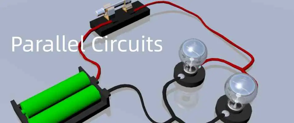
A parallel circuit is a closed loop electrical circuit that contains two or more electrical components such as resistors, inductors, capacitors, voltage sources, or current sources that are connected between the same two nodes. The basic configuration of components connected in parallel is that they share two common nodes and each component has its own two terminals or leads.
Parallel circuits are one of the two most basic arrangements for electrical networks, along with series circuits. But parallel and series circuits behave very differently in terms of voltage drops, current flow, resistance, and power dissipation. Understanding the rules and properties that govern parallel circuits is key for circuit analysis and effective electrical design.
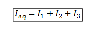
One of the defining characteristics of parallel circuit configurations is the way current flows when voltage is applied. The basic rules for current flow through the individual branches of a parallel circuit are:
The total current supplied by the source is equal to the sum of the branch currents flowing through each parallel component.
The current through each branch pathway is determined solely by the voltage applied and the resistance/impedance of that branch alone according to Ohm’s Law.
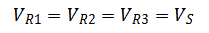
Each parallel branch has the same voltage drop across it equal to the source voltage.
The voltage drop across each branch is identical. Adding additional parallel branches does not affect the voltage across each existing branch.
This is illustrated in the simple parallel circuit below with three resistive branches. When a 12V source is applied, each resistor drops 12V across it. The source current equals the sum of the individual branch currents based on their respective resistances:
So in summary, the defining rules for current flow in parallel circuits are:
Total current is equal to the sum of branch currents
Voltage drop is the same across each parallel branch
Branch currents are determined by branch resistance and obey Ohm’s Law
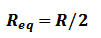
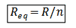
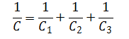
Calculating Equivalent Resistance
Although each branch in a parallel circuit sees the same voltage drop, the overall circuit can have an equivalent resistance different than the individual resistances. The combined or equivalent resistance of a parallel circuit can be calculated using the formula:
This combined resistance is lower than any of the individual resistances. Adding more parallel branches decreases the equivalent resistance as more current pathways are available.
Power Dissipation in Parallel Circuits
The power dissipated in each resistor in a parallel circuit follows the expected Ohm’s Law relationship:
$$P = I^2R$$
Where $I$ is the current through that resistor and $R$ is its resistance.
However, an important rule of parallel circuits is that the total power dissipated by the overall circuit is equal to the sum of the power dissipated in each branch:
$$P_{total} = P_1 + P_2 + … + P_n$$
So even though currents divide between parallel branches, powers add up. For the example circuit, the total power from the 12V source is:
This demonstrates that the source must provide enough power to match the sum of the power demands of the individual branches.
Applications and Examples
Parallel circuits are very common in electrical engineering applications. Some examples include:
Batteries in parallel – Batteries are often connected in parallel to increase the total current available from the power source. The voltage remains the same.
Electrical outlets – Outlets in a building are connected in parallel to provide independent power taps that each supply the full voltage.
Resistor networks – Parallel resistor combinations are used to create equivalent resistance values that can’t be achieved with a single resistor.
Integrated circuits – Very small resistors and other components are fabricated in parallel inside ICs to provide required functionality and performance.
Power distribution – High power systems use parallel branches to supply loads from grids and generators to reduce current per branch.
Electronics cooling – Fans and pumps can be connected in parallel to provide redundancy if one fails and share the thermal load.
Parallel circuits enable splitting currents, power sharing, redundancy, and circuit isolation. They follow predictable rules that are foundational for more complex circuit analysis.
What Happens in Open and Short Parallel Circuits
Parallel circuits exhibit some unique behaviors when branches are opened or shorted:
Open Branch
If a branch in parallel is opened, that branch no longer conducts current. However, voltage across the remaining branches stays the same.
Total circuit current decreases by the amount that was flowing in the opened branch. Equivalent resistance increases.
Shorted Branch
When a branch is shorted, its resistance drops essentially to zero. This creates a very low resistance path that pulls most of the current.
The shorted branch current is limited only by the source and wiring resistance. Other branch currents decrease. Equivalent resistance decreases toward zero. A direct short often blows a fuse.
So in summary, open branches decrease total current while shorted branches increase total current, assuming an ideal voltage source. These scenarios demonstrate the robustness of parallel circuits.
Troubleshooting Parallel Circuits
Some tips and techniques for troubleshooting issues in parallel circuits:
Check branch currents – a missing current indicates an open in that branch. Use Kirchhoff’s Current Law.
Check branch voltages – unequal voltages may indicate a bad connection increasing resistance.
Check for shorts between branches or to ground causing excessive current flow.
Measure equivalent resistance. Higher resistance points to an open branch. Lower resistance indicates a possible short.
Look for loose, corroded, or burnt connections causing unwanted changes in resistance.
Determine if current is sharing properly between branches. Mismatched resistances can lead to overloads.
Inspect components like resistors for physical damage which could produce opens or shorts.
Use a simulator to model the circuit and analyze effects of hypothetical faults.
Thorough understanding of parallel circuit rules combined with methodical troubleshooting procedures will help identify and remedy issues.
Comparison of Series vs Parallel Circuits
The properties of series and parallel circuits differ in important ways:
Property
Series Circuit
Parallel Circuit
Current
Same through all components
Divides among branches
Voltage Polarity
Drops add to equal source voltage
Same voltage across all branches
Resistance
Increases with more components
Decreases with more branches
Power Dissipation
Total power equals sum of components
Total power equals sum of branches
Component Failure Effect
Open disables circuit, short bypasses other components
Open removes branch, short increases total current draw
So while series strings components along one path, parallel branches components across multiple paths exhibiting very different characteristics. Both arrangements are critical to understand.
Frequently Asked Questions
What happens if one resistor opens in a parallel circuit?
If one resistor in a parallel circuit opens, that resistor branch no longer conducts current. However, the remaining parallel branches continue functioning normally. The overall equivalent resistance of the circuit increases. Total current flow decreases by the amount that was flowing in the now open branch. Voltage across each branch remains unchanged. The circuit continues working but at slightly reduced capacity.
How do you determine voltage, current, and resistance in a parallel circuit?
Voltage is the same across each branch by the definition of a parallel configuration.
Branch currents can be calculated using Ohm’s Law (I=V/R) based on the resistor values.
Equivalent resistance is found by taking the reciprocal of the sum of the reciprocals of the branch resistances according to the formula for resistors in parallel.
Why is total current equal to the sum of branch currents in parallel circuits?
This is a result of Kirchhoff’s Current Law which states that the algebraic sum of currents into a node must equal the currents flowing out of that node. In a parallel circuit, the incoming source current splits between the outward flowing branch currents. No current is lost, so the source current must exactly equal the sum of branch currents exiting the node for conservation of charge.
What happens when a parallel branch is shorted?
Shorting a branch provides an alternative low resistance path for current to flow. This will divert current from the other branches to preferentially flow through the shorted branch. The equivalent resistance decreases toward zero. Other branch currents will diminish as the short limits voltage. Eventually a large enough short circuit can draw more current than the source or wiring can provide, blowing a fuse.
How are parallel circuits used in electrical systems?
Some common uses of parallel circuits include:
Wiring buildings with multiple outlet circuits in parallel
Connecting batteries in parallel to increase capacity
Building redundancy into safety critical systems through paralleling components
Combining cooling fans and pumps in parallel for greater airflow or circulation
Adding capacitor or inductor branches to filter and smooth power supplies
Creating resistor ladder networks for analog to digital conversion
Sharing current and power demands among parallel branches
So parallel circuits enable splitting and redirecting electrical flows in many useful ways.
Summary
In summary, the key rules and properties that define parallel electrical circuits are:
Total current equals the sum of the branch currents
Voltage is the same across each parallel branch
Branch currents follow Ohm’s Law depending on branch resistance
Equivalent resistance decreases as more parallel branches are added
Total power dissipated equals the sum of power in all branches
Open branches decrease total current, shorted branches increase total current
Understanding parallel circuit fundamentals provides the basis for more advanced circuit analysis and design for electronics, power systems, and other electrical engineering applications.
Parallel Connection in Circuits:
The two components are said to be in parallel if they are connected back to back or end to end. The potential difference or the voltage drop across each component in parallel is same and the current flowing through each component is different.
Example 1 of Parallel Circuit:
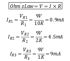
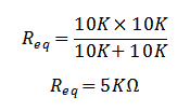
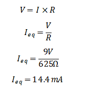
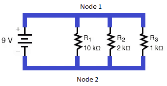
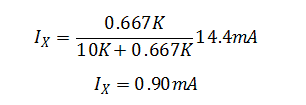
Let us understand from a basic circuit example where three resistors R1 (10KΩ), R2 (2KΩ) and R3 (1KΩ) are connected in parallel with each other. Now we will find out the voltage drop across each resistor, current through each resistor and total equivalent resistance of the circuit.
The voltage across each component connected in parallel is the same as the source voltage. Hence
Where VS is the source voltage = 9V battery
Current:
Now applying Ohm’s Law on each resistor to find current through each one.
Hence we can draw a simple table to represent these values
R1
R2
R3
Resistance (R)
10KΩ
2KΩ
1KΩ
Voltage (V)
9V
9V
9V
Current (I)
0.9mA
4.5mA
9mA
Equivalent Resistance of the Parallel Combination of Resistors:
Rule 1:
The equivalent resistance of the parallel combination of two or more than two resistors is always less than the value of smallest resistor in parallel.
Formula for equivalent resistance of more than two resistors connected in parallel is
Hence we can see that the equivalent resistance (R) is less than the smallest resistance (1K) in parallel.
Rule 2:
The equivalent resistance of two equal value resistors connected in parallel is half of that resistor value.
Formula for equivalent resistance of two resistors connected in parallel is
The rule 1 is also applicable for two resistors
Now let R1 = R2 = R = 10KΩ
Hence we can see that the equivalent resistance is exactly equal to half of the two resistance. We can say that
Rule 3:
In general, if “n” equal value resistors are connected in parallel, their equivalent resistance will be
Tips:
Convert all the units of resistances in one single unit. The units of resistance is mΩ, Ω, KΩ, MΩ
For calculation do not consider the milli, Kilo, or Mega units. Simply do math on numbers and add the unit to the final result.
Now back to the example 1, we can draw the equivalent circuit using equivalent resistor. Now we can calculate the total current (I) flowing through the circuit。
We can see that this total current is the sum of all the branch currents flowing through each resistor.
Hence we can say that
Nodes:
The node is the junction point where two or more terminals meet each other.
As we can see that the connection in blue color is shared between all components in parallel.
The node 1 is positive because it is connected to DC power source positive terminal and Node 2 is negative or GND (ground) terminal because it is connected to source negative terminal.
Rule 4:
If “n” equal resistors are connected in parallel, they will have equal current flowing through them and that current is
Where is the total / equivalent current of parallel circuit
Current Divider Rule:
The current divider rule says that the sum of all the branch currents connected in parallel is equal to the total current flowing.
Through the help of current divider rule we can find the individual branch current in Example 1.
The formula of current divider rule is
Where
As we calculated
Therefore
Hence it is proved from table.
The above discussion was in context of parallel resistor based circuits. However many other components can be connected in parallel
The parallel combination of resistors is very useful in many circuits where there is a need of a smaller resistor and you only have larger resistors available. Like if you have 2, resistors of 10K then you can make parallel combination to make it a 5K resistor. You can make it 20K also by connecting in series combination. Series combination will be discussed in later articles.
The combination of various passive components like resistor, capacitor and inductor can generate different functions. The parallel RLC circuit can be used oscillator circuits, frequency tuning and filter circuits. The application of parallel RLC circuit is basically in AC high frequency circuit however the above discussed resistor RLC circuit is for DC circuit application.
Parallel Battery Bank:
The DC batteries can be connected in parallel combination to make a battery bank with higher AH ratings. Three 18650 batteries each 3.7V/3000mAh connected in parallel will generate an equivalent bank of 3.7V 9000mAh. Thus voltage will remain same but the capacity of battery bank will increase.
Parallel Connected Capacitors:
The capacitors can be connected in parallel to increase the total/equivalent capacitance. The three capacitors C1, C2 and C3 10uF each connected in parallel will make an equivalent of 30uF capacitance (C)
Electrical Loads Connected in Parallel:
The household electrical wiring is done such that the electrical loads like Fans, Tube Lights, energy savers, Air-conditioners, Washing machines, Iron, Fridge and other appliances are connected in parallel to each other. The 220V/110VAC is supplied equally to each appliance and each appliance will draw current differently according to its wattage/power.
Fault in Parallel Circuits:
Open Circuit:
In Example 1, if one of the three resistors get open circuit, then the current will not flow from that resistor but the current will still flow from other two. The voltage will still be equal upon each resistor.
Similarly, if one of the three resistors get short circuit, the voltage drop across all three resistors will become zero. The current will flow at maximum from shorted resistor while the rest of the two resistors will have zero current flow.
The deployment of 5G networks is rapidly accelerating globally, with the new technology promising faster data speeds, lower latency, and the ability to connect massive numbers of devices. A key component that enables the functioning of 5G networks is the 5G printed circuit board (PCB). 5G PCBs facilitate the transmission of 5G signals and help achieve the high frequencies needed for 5G.
However, designing 5G PCBs comes with unique challenges compared to previous generations of wireless technology due to the higher frequencies used. New PCB materials and careful design considerations are required to account for signal loss, impedance control, thermal management, and more.
This comprehensive guide will provide electronics hardware designers and engineers with an overview of key considerations and best practices for designing 5G PCBs. Topics covered include:
5G frequency bands and data rate requirements
Selection of PCB materials and properties to consider
The frequencies used for 5G networks are a major difference compared to previous generations of wireless technology. 5G uses frequency bands in the high-frequency millimeter wave (mmWave) ranges between 24 GHz to 52 GHz, as well as some sub-6 GHz frequencies.
The advantage of mmWave frequencies is the availability of large amounts of contiguous spectrum which enables very high data rates. The mmWave bands currently defined for 5G use include:
n257 (28 GHz)
n258 (26 GHz)
n261 (27.5 GHz – 28.35 GHz)
Some of the key 5G frequency bands and corresponding data rates include:
Frequency Band
Data Rate
600 MHz
100 Mbps
2.5 GHz
1 Gbps
4.7 GHz
1.3 Gbps
24 GHz
3 Gbps
28 GHz
5 Gbps
39 GHz
7 Gbps
However, the higher frequency mmWave signals also have much shorter wavelength and cannot penetrate obstacles as well. This leads to higher path loss and requires more advanced antenna technologies like massive MIMO and beamforming.
When designing a 5G PCB, the frequency bands and data rate requirements need to be carefully considered to ensure the board can support high frequency signals with adequate gain and minimal loss.
PCB Substrate Materials for 5G
The selection of the appropriate PCB substrate material is critical for 5G design. The dielectric substrate material separates copper layers in the PCB and impacts loss tangent, dielectric constant, thermal conductivity and other properties. Some key considerations for 5G PCB substrate selection include:
Dielectric Constant
A low dielectric constant (Dk) helps reduce signal loss and cross talk. Common low Dk substrates for 5G PCBs include fluoropolymers like PTFE (Dk of 2.1) and liquid crystal polymers (LCP) with Dk between 2.9-3.3.
Loss Tangent
The loss tangent indicates the material’s inherent signal loss due to dielectric absorption. Lower loss tangent values below 0.005 are desirable for mmWave 5G boards. Rogers RO3000 series laminates have loss tangents between 0.0021-0.0027.
Thermal Conductivity
The high power density of mmWave circuits leads to substantial heat generation. Using thermally conductive substrates like ceramic aluminum nitride (170 W/mK) and liquid crystal polymer (0.67 W/mK) helps dissipate heat.
Coefficient of Thermal Expansion (CTE)
Matching CTE between PCB and components prevents solder joint failure and pad cratering during thermal cycling. Glass reinforced hydrocarbon laminates offer CTE compatibility with common components.
Moisture Absorption
Materials like PTFE have very low moisture absorption, helping maintain stable electrical performance. High moisture absorption of substrates should be avoided.
Thickness
Thinner dielectrics help reduce loss at mmWave frequencies. While thickness depends on layer count, substrates between 0.1mm to 0.3mm thickness are typical for 5G.
Here is a comparison between some popular 5G PCB substrate materials and their properties:
The layer stackup defines the number of copper and dielectric layers in a PCB. An optimal stackup is important for controlling impedance, minimizing loss and ensuring signal integrity at 5G frequencies. Here are some key guidelines for 5G PCB stackups:
Use thicker copper layers (2oz/ft2 or more) to reduce conductive losses
Minimize number of lamination cycles to limit signal loss
Include ground planes close to signal layers for impedance control
Keep layer count low, typically 4-8 layers for optimum 5G performance
Use symmetric stripline configurations for differential pairs
Manage layer transitions carefully using tapers/chamfers
Adopt a split power plane approach to isolate noise-sensitive supplies
Allow for thermal vias beneath hot components to dissipate heat
A sample 8 layer stackup for a high frequency 5G board could be:
Layer
Function
Thickness
1
Signal
2 oz Cu
2
Ground
1 oz Cu
3
Power
2 oz Cu
4
Signal
2 oz Cu
5
Ground
1 oz Cu
6
Power
2 oz Cu
7
Ground
1 oz Cu
8
Signal
2 oz Cu
The close proximity ground planes help control impedance, reduce EMI, and minimize crosstalk. The split power planes isolate digital and analog supplies. Thicker 2oz copper minimizes conduction losses.
5G PCB Layout Guidelines
Careful attention must be paid to the PCB layout to achieve design objectives for 5G performance, signal integrity and EMI control. Some key 5G layout techniques include:
Controlled Impedance
Maintain 100 Ohm differential impedance for interface traces by tuning trace width/spacing based on stackup. Minimize length differences between differential pairs.
Isolation Between RF and Digital
Separate RF and digital sections on layout using ground/shielding barriers. Prevent noise coupling by distance and orientation.
Minimize Trace Lengths
Keep trace lengths as short as possible on mmWave nets to reduce insertion loss. Use surface mount devices for shorter connections.
EMI Shielding
Incorporate shielding cans, guard traces, and ground/power moats to contain EMI emissions. Prevent slot antennas from forming.
Power Delivery Network
Use enough decoupling capacitors close to IC pins, and lower impedance power distribution for clean, stable supply rails.
Thermal Management
Allocate space under hot devices for thermal vias/metal slugs to conduct heat. Use internal cutouts/keepout zones for airflow.
Antenna Integration
Properly integrate antenna arrays within board or align edge mounts using cutouts and milling. Match impedance.
Test Points
Include test/probe points to validate performance over frequency, such as with network analyzers and TDR measurements.
With careful implementation of these guidelines, the PCB layout can be optimized for superior 5G signal integrity.
Maintaining signal integrity and minimizing loss is critical for 5G PCBs due to the higher frequencies involved versus 4G or Wi-Fi. Some techniques to help mitigate loss and improve signal performance include:
Extensive Ground Stitches
Connecting all ground planes and areas with many via and microvia stitches reduces ground inductance.
Backdrilling (Via Stub Removal)
Backdrilling unused portions of plated through holes improves impedance matching and reduces reflections.
Buried/Blind Vias
Using vias that span only 2-3 layers controls coupling compared to full-depth drilled vias.
Maintaining adequate clearance from ground layers prevents energy loss through substrate radiation.
Matched Length Routing
Tuning trace lengths to match electrical lengths improves insertion loss in differential pairs.
Periodic Voiding
Introducing voids along a reference plane reduces eddy current losses at high frequencies.
Dielectric Coatings
Applying low-loss tangent coatings (e.g. paralene, PTFE) on traces cuts down on surface wave propagation loss.
With careful modeling and simulation, these techniques can be implemented to fine-tune 5G board performance.
Thermal Management Approaches
Thermal management is a significant concern for 5G PCBs due to increased power densities at mmWave frequencies. Here are some approaches to effectively dissipate heat:
Metal core substrates – Base laminate itself is aluminum or copper for spreading heat
Thermal vias – Drilled holes filled with metallization conduct heat to inner layers
Heatsinks/heat-spreaders – Use machined aluminum heatsinks with thermal interface material
Fans/air flow – Incorporate small fans or ventilation channels into enclosure
Phase change materials – Substrates with materials that undergo phase change to absorb heat
Vapor chambers – Hollow chamber with working fluid that evaporates and condenses, transferring heat
Ideally, thermal management techniques should be modeled during design to predict temperature gradients and optimize heat flow.
EMI Control Methods
EMI control is necessary in 5G designs to prevent interference with other devices and ensure conformance to EMI/EMC standards. Methods to control EMI include:
Metal shielding cans over sensitive ICs
Small aperture waveguide vents on enclosures
Ground plane stitching through multiple layers -strategic placement of ground vias forming “walls”
Filtering components like ferrite beads on I/O
Additional shielding gaskets on enclosure seams
Internal metal compartmentalization to prevent slot antennas
Careful component placement to contain noise sources
Sparse power plane fills with islands disconnected at DC
Prototyping and testing needs to validate EMI performance. It may be an iterative process as issues are found and fixes incorporated. Shielding, filtering and isolation are key principles to follow for managing EMI and EMC.
Testing and Validation
Throughout the PCB development process, testing and validation should be conducted using the following methods:
Simulation and Modeling
Perform 3D EM simulations of traces, stackup, PDN, thermal performance. Identify problem areas through modeling.
Frequency Sweeps
Use a network analyzer for insertion loss, return loss, and impedance measurements over frequency. Verify input to output magnitude and phase.
VSWR and Losses
Evaluate voltage standing wave ratio (VSWR), gain, and losses. Look for impedance discontinuities and unexpected resonances.
Eye Diagrams
Eye diagrams show signal integrity and jitter. A widely open clear eye is desired for clean signaling.
Time Domain Reflectometry
TDR plots will reveal impedance mismatches and discontinuities along a trace from reflections. Useful for controlled impedance validation.
Vibration/Shock
Assess mechanical robustness under vibration and shock conditions. Check for solder joint cracks or trace/via fractures.
Thermal Imaging
Use an IR thermal imaging camera to map board hot spots and temperature gradients. Identify cooling deficiencies.
EMI Diagnostics
Test for radiated and conducted EMI compliance. Sniff out specific noise sources.
With careful testing and validation, potential issues can be caught early and addressed to ensure optimal 5G board performance.
Conclusion
Designing printed circuit boards for 5G applications presents new challenges compared to previous wireless generations due to the use of mmWave frequencies and higher data rates. However, through careful planning and optimization across PCB materials selection, stackup design, layout considerations, thermal management, and EMI strategies, a high performance 5G board can be realized.
By following the guidelines and techniques outlined in this article, PCB designers can fully unlock the capabilities of 5G technology and facilitate the rollout of faster, lower latency 5G networks. With attention to signal integrity, thermal management and EMI control, the next generation of wireless connectivity can be achieved through optimal 5G PCB implementations.
Frequently Asked Questions
Q: What are some key differences between designing PCBs for 5G vs 4G?
A: Some key differences include:
5G uses higher mmWave frequencies between 24-52 GHz requiring attention to loss, impedance control and thermal issues. 4G uses lower frequency bands.
Shorter mmWave signal wavelengths require smaller PCB features and tighter layout tolerances.
5G PCB materials favor low-loss, thermally conductive substrates whereas FR-4 was common for 4G.
Beamforming antennas and higher power density ICs lead to greater thermal challenges.
Shorter mmWave signal paths, isolation and EMI control are more critical in 5G design.
Q: How can signal loss issues be identified in 5G PCB design?
A: Methods to identify signal loss issues include:
Performing insertion loss simulations on critical high speed nets
Using TDR analysis to find impedance discontinuities causing reflections
Evaluating S-parameter results from VNA tests for excessive loss at 5G frequencies
Analyzing eye diagrams for signs of signal degradation from loss or distortion
Measuring channel operating margin and link budgets to model expected vs actual loss
Thermal imaging to check for excessive heating of traces causing resistive losses
Q: What are some methods to control EMI for 5G boards?
A: Techniques to control EMI in 5G PCB design include:
Use of shielding enclosures and cans to contain emissions
Careful component placement and orientation to avoid noise coupling
Extensive ground plane stitching to reduce ground loop antennas
Strategic use of ground/power moats around circuits
Filter components like ferrites beads to suppress noise
Limiting slot/aperture openings in enclosures
Sparse fills and islands on power planes to reduce coupling
Tight board-to-chassis grounding to shunt EMI away
Prototyping and testing to identify issues and refine design
Q: How can signal integrity be maintained for sensitive 5G links?
A: Some best practices for maintaining signal integrity include:
Matched length differential pairs to control skew and dispersion
Cross-talk mitigation through distance and routing orientation
Choosing low loss PCB materials and laminates
Adding low loss coatings on traces when needed
Proper backdrilling of unused via sections
Careful design of transitions between layer changes
Simulation and characterization of channel frequency response
Managing noise through isolation and filtering
Minimizing trace lengths whenever possible
Q: What kind of validation testing should be done on 5G PCB prototypes?
A: Recommended validation tests include:
Frequency domain measurements using VNAs to characterize insertion loss, return loss, VSWR
Time domain analysis with TDR to find impedance discontinuities
Signal integrity checks using eye diagrams, jitter analysis
EMI testing for radiated and conducted emissions
Vibration and shock testing for mechanical integrity
Thermal imaging and measurement of temperature gradients
Functional testing to verify performance under use conditions
Correlation to simulation models and results
5G PCB Technology – A Revolution in Telecommunication Industry
If you want 5G PCB design suggestions or need 5G PCB Manufacturing service,Pls send email to sales@raypcb.com , You will get reply in short time.
5G technology
5G Pcb Board
The 5G (stands for 5th Generation) technology is the whole new innovation in the field of telecommunication industry. It is the iteration of existing cellular 4G LTE (Long Term Evolution) technology. This 5G technology can break the records of high speed and reliable internet connection, cellular and satellite communication. It is estimated that average download speed of up-to 1GBps and the data rates as high as 20 GBps with latency less than 1mS is possible. This is astonishingly amazing to know that this high speed communication can open new doors to various applications in small
and large businesses, entertainment and multimedia, smart home, autonomous driving in automobile sector, Medical field in surgery, technology, mobile, and satellite communication and in IoT.
Latency: It is the time required by data to travel from source to destination.
The high speed 5G technology can enable the real time control and monitoring of machines and devices like robots, drones, automobiles, and other machines that will transmits feedback signal to the operator and receives command signals in response, this all done in high speed communication link.
4G Vs 5G Technology:
Parameters
4G
5G
Latency
10ms
1ms or less
Max Data Rate
1 Gbps
20Gbps
Transmitted Power
23dbm except for 2.5GHz TDD
26dbm at 2.5GHz and above
No of Mobile Connections
8 billion
11 billion
Frequency Range
600 MHz to 5.925 GHz
600 MHz to 28,39 and 80 GHz (mm wave technology)
Channel BW (Band Width)
20 MHz
100 MHz for 6 GHz400 MHz for above 6 GHz
Uplink Wave form
SC-FDMA
CP-OFDM
Download speed
100 Mbps
10,000 Mbps
Deployment Year
2006-2010
2020
User Data BW (Practical Analyses)
Mobile = 10-30MbpsFixed = 50-60 Mbps (cm wave)
Mobile = 80-100 MbpsFixed = 1-3 Gbps (mm wave)
Coverage per Antenna & Usage
Mobile = 50-150 Km (City, Rural area)Fixed = 1-2 Km (High Density Area)
Mobile = 50-80 Km (City, Rural area)Fixed = 250-300 meter (High Density Area)
The cellular networks are actually the cluster of small cells and these cells are further divided into sectors. In 4G LTE, the high power towers of cell are transmitting electromagnetic radiation to cover longer distances. However on the other hand 5G uses small towers mounted at every 1 Km on different types of high elevated places like rooftops and poles in large quantity. These many small cells transmit radiation of the wavelength of the order of few millimeter. These millimeter electromagnetic waves can travel smaller distances and travel in line of sight hence it is hindered by any physical objects like tall buildings and can be disturbed by weather conditions as a result degrading the signal strength.
The lower frequency spectrum of 5G can reach longer distance but data rates will be compromised while mm wave have smaller distance but higher data rates.
(Fig- 5G Cellular Network Base Station Types)
What is mm Wave..?
The millimeter (mm) wave spectrum falls in the frequency range of 30 GHz to 300 GHz. This phenomenal range of frequency has the wavelength of 1mm to 10mm. The mm wave are also known as VHF or EHF Very High Frequency or Extremely High Frequency respectively names given by ITU.
The mm waves are susceptible to heavy rainfall. The mm wave signal strength will drop when heavy droplets of rain interfere with mm wave i.e when the size of droplet or ice crystals reach the size of mm wave which is about few inches, then severe attenuation will be observed. This is also for snowy season with thick/dense blizzards are observed. This phenomenon is commonly known as “Rain Fade” or “Rain Loss”. This phenomenon can affect the satellite communication in LEO, MEO and GEO earth orbits. This phenomenon can also hinder GPS signals. Licensed bands from FCC are 71-76 GHz, 81-86 GHz and 92-95 GHz to operated point-point high BW. Unlicensed band for short range communication can be done on 60 GHz mm wave spectrum
Unlike passive antennas that are used in common RF communication which are made of metal rods, 5G antennas are active antennas having semiconductor devices embedded inside the antenna. High speed 5G dedicated PCB design and fabrication is utmost important for 5G antenna PCB and associated circuitry. At Rayming PCB we have developed state of the art 5G PCB. Please check out the snapshot of our 5G PCB.
The basic technique used is the beam forming which allows the 5G antenna to emit radiation in a particular direction or pattern instead of emitting equally in all directions. The 5G antenna is made of massive MIMO (Multiple Input Multiple Output) antennae. The massive / large number of antenna elements are used in phased array shape and different sizes are available. The individual antenna element size is small but are used in 100s to make dense array.
As a result the radio waves are directed to the targeted users with the help of advanced algorithms that determine the best route for radio waves to reach the end user. This phenomenon is known as beam steering. The beam steering is very effective and optimizes the power consumption and increase efficiency by eliminating the unwanted Omni directional radio transmission. As a result very high throughput thus allowing more people to connect simultaneously
5G Technology Applications:
High Speed Cellular Network
As discussed above, the extremely high data rates enable the calling, messaging and multimedia services to speed up and faster communication is possible. So no worry about call dropping and undelivered text messages or slow internet. 5G technology will give you unstoppable high speed services
Entertainment and Multimedia:
Now you can enjoy Netflix, Watch Live shows or download your favorite TV program, movies in the blink of an eye. Yes literally..! This is possible because of 5G high download speed up-to 10Gbps.
The smart devices will be using 5G technology to connect to our mobile devices using wireless network for monitoring and control. High speed 5G connectivity can enable CCTV cameras to transmit live video streaming to our mobile devices
Logistics
High speed communication 5G link will enable logistics tracking, management and delivery of shipment online on our cell phones
5G in Farming
Smart chips like RFID will be used in livestock to track position and activity. Smart agricultural machines can be controlled remotely through speedy 5G link.
Medical Surgery
Live video streaming inside the patient’s body for transplant and operation is possible today due to 5G
Autonomous Driving
In future, automatic cars will be on roads. Cars will interact with traffic signals and can communicate with other cars by means of 5G high speed link. This enable those to detect an obstacle in matter of milliseconds (latency of 5G) and to avoid collision.
FPGA stands for Field Programmable Gate Array. An FPGA is an integrated circuit that can be programmed or configured by the customer or designer after manufacturing. This allows the FPGA to be customized to perform specific functions required for an application.
FPGAs contain programmable logic blocks and interconnects that can be programmed to implement custom digital circuits and systems. Unlike microprocessors that have fixed hardware function, the hardware logic and routing in an FPGA can be changed as needed by reprogramming. This makes FPGAs extremely versatile for many applications.
Some key capabilities and benefits of FPGAs include:
Customized hardware functionality
Parallel processing for high performance
Reconfigurable digital circuits
Prototyping and testing new device designs
Flexible I/O configurations
Low power consumption
Short time to market
FPGAs are widely used for prototyping of new custom ASIC designs, specialized parallel processing applications, aerospace and defense systems, automotive systems, IoT and embedded devices, and other applications requiring flexible or high-speed processing.
Major manufacturers of FPGAs include Xilinx and Intel (formerly Altera). There are many different types of FPGAs optimized for applications like high-speed processing, DSP, low power, or high I/O density.
The concept of field programmable logic devices emerged in the 1980s to fill a gap between inflexible application-specific integrated circuits (ASICs) designed for a specific task and programmable microprocessors that lacked performance for many niche needs.
In 1984, Xilinx co-founders Ross Freeman and Bernard Vonderschmitt invented the first commercially viable field-programmable gate array. This allowed circuit designers to configure the interconnections between a set of logic blocks to create custom digital circuits by programming rather than manufacturing a new chip each time.
Other FPGA companies like Actel (now Microsemi) soon followed in bringing programmable gate arrays to market. Early FPGAs were relatively simple with 1-10k gates and used in glue logic applications. As silicon manufacturing advanced, FPGA density and capabilities grew rapidly.
By the 1990s to 2000s, FPGAs with tens of thousands to over a million gates became more common. This allowed implementation of complex systems like entire microprocessors within a single FPGA chip.
FPGA architectures also evolved to add more embedded functions like memory blocks, DSP slices for math processing, programmable I/O, high-speed transceivers, and embedded microprocessor cores. Major vendors today like Xilinx and Intel produce FPGAs with billions of transistors capable of extremely sophisticated and demanding processing tasks.
FPGA Architecture Basics
The internal architecture of an FPGA consists of the following major components that can be configured:
Configurable Logic Blocks (CLBs) – The basic logic units that can implement simple Boolean functions and more complex functions. CLBs contain “look-up tables” that allow them to be programmed to perform any logic operation.
Input/Output Blocks (IOBs) – Provide the interface between the I/O pins on the FPGA chip package and the internal configurable logic. Support various signal standards.
Interconnects – The programmable routing between CLBs and IOBs. Allows flexibility in connecting internal components to implement a desired circuit function. Can include various lengths and types like global, regional, direct connects.
Memory – Many FPGAs include dedicated blocks of memory that can be used by the circuits mapped into the device. Saves integrating separate memory chips.
Embedded IP – Hard IP processor cores, DSP slices, PCIe interfaces, transceivers and other built-in functions may be included on higher performance FPGAs to optimize them for target applications.
Clock Circuitry – Managing and distributing clock signals across the FPGA is critical. Clock inputs, PLLs, DLLs, and clock buffers help achieve this.
The user programs the FPGA by specifying the Boolean logic functions for the CLBs, the interconnect wiring between blocks/IOs, use of memory and embedded IP, clocking resources, and I/O settings. This overall programming is called the configuration.
FPGA vs ASIC Differences
Xilinx Zynq fpga
FPGAs differ in important ways from Application Specific Integrated Circuits (ASICs):
FPGA
ASIC
User programmable after manufacturing
Custom manufactured for fixed function
Reconfigurable – logic can be updated
ASIC function is fixed once produced
Easier to prototype and implement changes
Costly and slow to change function once made
Parallel processing well suited for data flow applications
Often better performance and efficiency for fixed function
Generally lower volume applications
Higher volume justifies design costs
Lower development costs
Much higher development and fabrication costs
FPGAs are more flexible and quicker to develop with but less optimized in final form factor or performance than a custom ASIC. The reconfigurability and lower cost of FPGAs make them popular for low and medium volume products where custom ASICs may not be justifiable. FPGAs are also widely used to prototype ASIC designs for testing before committing to ASIC fabrication.
FPGA Design Flow
The general workflow to implement an application with an FPGA consists of the following steps:
Design Entry – The digital logic to be implemented is captured using a hardware description language like VHDL or Verilog or a schematic diagram. This is the source code describing the desired hardware functionality.
Synthesis – The source code is synthesized into lower-level Boolean logic gate representations and optimized for the target FPGA architecture.
Simulation – The design is simulated pre- and post-synthesis to verify correct functional behavior. Simulation aids debugging.
Place and Route – The logic gates are “placed” into specific FPGA hardware resource blocks and “routed” together using available interconnect paths.
Bitstream Generation – The placed and routed design is converted into a binary file that programs the FPGA configuration. This file is called the bitstream.
Configuration – The bitstream is loaded into the FPGA device to actually configure its hardware resources to implement the user’s design.
In-System Verification – The real world functionality on the FPGA is tested and debugged after configuration and integration.
FPGA vendors provide design and programming software tools to assist and automate this design flow. Popular tools include Xilinx Vivado and Intel Quartus Prime. HDL languages like VHDL and Verilog are used for design entry.
FPGA Programming Technologies
Several methods and technologies exist for programming the configurable logic in an FPGA:
SRAM Based – SRAM cells control the logic and interconnect configuration of the FPGA. Volatile, needs reconfiguring on power up. Most common approach used by major vendors.
Antifuse – One time programmable connections between logic blocks. Used in some lower cost FPGAs. Permanent once programmed.
Flash/EEPROM – Flash or EEPROM cells used for configuration cells. Allows reprogramming but nonvolatile so retains configuration on power loss.
CPLD – Complex Programmable Logic Devices have architecture between PALs and FPGAs. Smaller with more predictable timing.
Security/Encryption – Advanced FPGAs may have encryption and authentication protections on bitstreams to prevent IP theft.
SRAM programming is dominant due to its combination of reconfigurability and density. Antifuse, Flash and CPLD serve niche lower density roles. Security features help protect FPGA IP designs.
Major Applications of FPGAs
The flexibility and performance of FPGAs make them very attractive for many advanced applications including:
Aerospace and Defense – Used in guidance systems, radar processing, satellites, and mission computers where radiation-hardened FPGAs provide reconfigurable reliability.
IoT/Embedded – Provide custom logic, low power consumption, and small form factors needed for sensors, wireless, and battery-powered devices.
Image/Video Processing – Hardware acceleration for algorithms like convolutional neural networks, encoding/decoding, and analytics.
5G Telecom – High speed connectivity and processing for networking gear using FPGAs with high bandwidth I/O and DSP.
AI Acceleration – FPGA inference engines that provide optimized parallel processing for neural networks and machine learning.
Prototyping – FPGAs used to model and verify functionality of new ASIC designs before manufacture.
FPGAs continue growing in capability and bridging into applications traditionally addressed by CPUs and GPUs. Their flexibility makes them the ideal choice when custom hardware acceleration is needed.
The FPGA market continues to see intense innovation and new entrants even as it consolidates around Xilinx and Intel. The growth of 5G, AI, embedded vision, and other applications is driving demand for more advanced programmable logic solutions.
Trends and Innovations in FPGAs
FPGAs continue to evolve rapidly to increase capabilities and provide advantages over other processing technologies for specialized requirements:
Heterogeneous Integration – Combing FPGA fabric with hard processor cores (ARM, RISC-V), transceivers, memory, analog, etc. on a single chip provides “system-on-chip” capability.
High Level Design – Raising design abstraction above HDLs by using C/C++, OpenCL, MATLAB, and other languages to describe FPGA behavior. This expands accessibility.
3D Packaging – Stacking FPGA dies and integrating with other dies like HBM memory enables much higher bandwidth and density.
Security – Root of trust, bitstream encryption/authentication, and other features to protect FPGA configuration and IPs from tampering or theft.
Cloud/Datacenter – Adoption in public cloud FaaS offerings and datacenter acceleration using FPGAs for their flexibility and performance per watt.
Soft MCUs – Soft microcontroller cores implemented internally within an FPGA for low cost embedded applications.
AI Acceleration – Optimized FPGA deep learning processors for inference using low precision and quantization to achieve efficiency.
FPGAs will continue to blur into adaptive computing devices as they evolve beyond basic programmable logic into heterogenous systems-on-chip. Their flexibility to reconfigure hardware logic on the fly makes them a foundational technology for the future.
Frequently Asked Questions
What are the main differences between FPGAs and CPLDs?
Complex Programmable Logic Devices (CPLDs) differ from FPGAs in several ways:
Less logic capacity – typically thousands not millions of gates
Based on sum-of-products architecture
Optimized for predictable timing
Live at power up (no configuration bitstream)
Often lower cost and power
Can be built-in flash/OTP instead of SRAM
So CPLDs serve simpler glue logic roles rather than implementing complex systems like FPGAs.
What are the advantages of using VHDL vs Verilog for FPGA design?
VHDL tends to be preferred for larger ASIC and FPGA designs requiring rigorous verification for manufacturability. Verilog started as a simulation language and is popular with front-end designers. Key differences:
VHDL
Strongly typed, English-like syntax
Large set of data types
Excellent tool support
Suited for verification & top-down modeling
Verilog
C-like syntax, weaker typing
Fewer data types
Suited for behavior modeling
Fast simulation, prototyping
Widely used in education
How are FPGAs programmed/configured?
Most FPGAs are SRAM-based and programmed by loading a bitstream:
Design logic is created and outputs a binary bitstream file after place & route
On power up, bitstream loads from flash/storage into SRAM cells
SRAM settings define logic, I/O config, routing to implement design
This can be reprogrammed by flashing a new bitstream
So FPGAs provide complete hardware configurability via programmable SRAM-based bitstreams.
What types of CAD tools are used for FPGA design?
Common FPGA CAD tools include:
Xilinx Vivado – For synthesis, place & route, bitstream gen
FPGA vendors like Xilinx provide integrated environments that take design entry through bitstream. Additional tools help with simulation, PCB design, IP reuse, and C-level design.
What are the main challenges when working with FPGAs?
Some common challenges with FPGA design include:
Steep learning curve programming with HDLs like Verilog and VHDL
Complex toolchains require expertise to optimize through the flow
Timing closure and routing congestion as designs push capacity limits
Power usage control and thermal management
Debugging within hardware description languages
Cost of tools and IP add to development overheads
Staying current as architectures rapidly evolve
But continuous improvements in design tools, abstraction levels, and embedded debug capabilities are helping overcome these challenges.
Summary
FPGAs are integrated circuits whose logic and routing can be reconfigured after manufacturing. This provides hardware-level flexibility compared to fixed-function ASICs. FPGAs contain logic blocks, I/Os, and interconnects that can be programmed using HDL or schematic design entry.
Leading FPGA applications include aerospace/defense systems, 5G infrastructure, automotive electronics, IoT devices, and hardware acceleration for AI inferencing. Major vendors are Xilinx and Intel/Altera, but new entrants continue to push innovation in FPGAs for embedded, cloud computing, networking, and other uses.
Trends in FPGA evolution include heterogenous integration, raised abstraction levels, 3D packaging, and security. As FPGAs grow beyond basic programmable logic into adaptive computing platforms, they will play an increasingly important role in diverse electronic systems.
An Introduction to FPGA
FPGA stands for (Field Programmable Gate Array). As the name implies, the FPGA is an integrated circuit (IC) that is basically an array of logic gates and is programmed/configured by the end user in the field (wherever he is) as opposed to the designers.
The basic logic gates are the core building blocks of the FPGA. It is not like the FPGA IC is full of these logic gates, but FPGA is based on digital sub-circuits carefully interconnected with each other to perform the desired function. It is like for example to make a shift register the AND gates and OR gates ICs are required, so there are two ways either to buy these individual ICs and interconnect them together to obtain the functionality of Shift register. The other way is to buy a shift register IC instead and make your design much more compact.
This is the case with FPGA assembly, the sub-circuits are already made of basic AND, OR and NOT gates and these sub-circuits are then interconnected very accurately to design the internal hardware blocks called Configurable Logic Block (CLB).The CLBs can also be defined as Look up Tables (LUT) that is programmed by Hardware Description Language (HDL) to achieve desired output.
These thousands of CLBs are then connected with IOBs to interface with external world circuitry. The IOB stands for “Input Output Blocks”. These IOBs are made of pull up, pull down resistors, buffer circuitry and inverter circuits.
Reprogram-ability of FPGA:
The biggest advantage of FGPA is its ability to be reprogrammed at the field. Its flexibility to be used as microprocessor, graphic card or image processor or all of them at the same time make it solid upper hand to basic micro-controllers or micro-processors.
These FPGAs are programed by HDL like VHDL or Verilog. Some additional features are being added nowadays in FPGAs like dedicated hard-silicon blocks for attaining functions of External Memory Controllers, RAM block, PLL, ADC and DSP block and many other components.
Difference between the Micro-controller and FPGA:
Today, many of the projects are based on micro-controllers. As our trend in developing student project, professional circuits, industrial products development is based on micro-controller based circuits, we did not got much familiarized with FPGAs.
The main difference between the micro-controller and FPGA is that, “A micro-controller is versatile IC and can be programmed in different ways to fit in various types of applications while the FPGA is a dedicated IC specifically designed to perform special functions according to the needs of a particular application”.
Another important difference is that “The FPGAs are hardware Configurable Logic Blocks (CLBs) based ICs that can be interconnected to external circuits through Hardware Description Language HDL codeby means of IOBs while micro-controllers are based on software/programming/coding where instructions are executed sequentially.”
The micro-controller / micro-processor has constraints of inability to execute multiple instructions simultaneously and also functionality you want to perform must have the availability in instructions sets of a particular controller/processor.
The FPGAs are somewhat similar to ASIC “Application Specific Integrated Circuits” but not very much. The key difference in FPGA and ASIC is that CLBs in FPGA can be reconfigured to perform different task/operation/function but in the case of ASIC the dedicated ASIC chip will perform the same operation for the entire life time for which it was designed.
The analogy of FPGA and ASIC is that you build a house using LEGO parts, then you demolish it and built a car using same LEGO parts. These LEGO parts are same as CLBs of FPGA.
The analogy of ASIC is that you build the same house using concrete blocks and cement (not the LEGO) but now you cannot demolish it and build other thing from this. This work is permanent. Hence this is ASIC.
So the ASICs are dedicated ICs in which digital circuitry (logic gates and sequential circuits) is hardwired or permanently connected internally on silicon wafer.
FPGAs are suitable for low volume production and require much less time and money as compared toothier ASIC counterparts. FPGAs require less than a minute to reconfigure. Another important advantage is that FPGAs can be partially reconfigured and rest of FPGA portion is still working.
However, FPGAs on the other hand are slower and more power hungry due to their large area size due to dense routing programmable interconnection. This complex interconnection accounts for 90% of the total size of FPGA.
Detailed Insight of FPGA Structure:
The main constituents of FPGA are
Configurable Logic Blocks (CLBs)
Input Output Blocks (IOBs)
Switch Box (SB)
Connection Box (CB)
Look Up Table (LUT)
Horizontal and Vertical Routes
Configurable Logic Block (CLB):
A CLB is made up of the cluster of BLE (Basic Logic Element) through a dense interconnect scheme. A BLE has the multiplexer, SRAM and D Type Flip Flop. These three components forms the BLE and the cluster of BLEs form the CLB
Input Output Blocks (IOBs):
These are the blocks that make interconnection between the FPGA and outside circuitry. The IOBs are the end connection of the programmable routing network.
Switch Box (SB):
Switch Box is the collection of switches to connect different horizontal and vertical routes (tracks). Ability of a track to connect to multiple tracks is defined as the connectivity of SB.
Connection Box is the collection of switches to connect CLB to multiple routes. Ability of the CLB to connect to multiple routes/tracks is defined as the connectivity of CB
Look Up Table (LUT):
The lookup table is made of multiplexer and SRAM. A 4 input LUT requires (24) 16 SRAM bits to implement a 4 bit Boolean expression.
Horizontal and Vertical Routing Channels:
The horizontal and vertical lines/routes that creates the mesh network of FPGA
Flexibility of CB:
The flexibility of CB is defined as (FC). A FC = 1 means that all the adjacent routing channels are connected to the inputs of CLB
Flexibility of SB:
The flexibility of SB is defined as (FS). It is defined as the total number of tracks with which every track entering the SB connects to.
Conclusion:
It is therefore concluded that FPGAs have advantages over other options like ASIC and microprocessor / micro-controller in the sense that FPGAs are handy and easily reconfigurable at the user end. It can be customized by a simple HDL code and are easily available in the market for reasonable rates between 50 to 100 USD.