While searching for some affordable environmental sensors, we came across the popular and seemingly ideal BME280. This sensor is the digital I2C type, which can function at either 1.8V or 3.3V, offering measurements of barometric pressure, humidity, and temperature consuming low energy in the process and working with high accuracy at affordable and low cost. This is why it is great for temperature monitoring, weather stations, etc.
Due to this, we decided to buy some BME280 sensors from some sellers. However, on two occasions, we got BMP280, which is lesser compared to the BME280. The difference between bmp280 vs bme280 is that the BMP280 has a different ID and lacks humidity measurement. So using the BMP280 didn’t give the desired results and it felt like we made a mistake. This is why we are writing out this information to help you in case you have been supplied a different product and don’t know the difference between bmp280 vs bme280.
Grove BMP280 Barometer Sensor: What is this?
The grove barometer sensor has a high precision and low-cost sensor, which measures the barometer and temperature. Furthermore, this sensor supports the SPI and I2C communication.
It is known as a tiny and cheap atmospheric sensor breakout that helps in measuring barometric pressure and temperature, without having to take up much space. You can get everything you need to know just from its tiny breakout.
This breakout was specially designed for outdoor/indoor navigation, home automation, weather forecasting, wellness monitoring, and personal health. The module makes use of Bosch-manufactured environmental sensors with barometric pressure, temperature sensor, which is the upcoming generation upgrade of the well known sensor BMP183/BMP180/BMP085.
This sensor serves all weather sensing types and will even work effectively for both SPI and I2C. This Bosch’s precision sensor is regarded as the best precision sensing, low-cost solution for the measurement of barometric pressure having an absolute accuracy of ±1.0 hPa and a temperature measurement accuracy of ±1 degrees centigrade.
Due to the fact that pressure changes with respect to the altitude, the measurements of pressure are so accurate and good that it can also serve as an altimeter having an accuracy of ±1.0 meter.
BMP280 can be regarded as the next generation of sensors. It upgrades the BMP183/BMP180/BMP085 having altitude with low noise of 0.25m. Its conversion time is also similar and fast. Specifications here are also the same and can utilize either SPI or 12C. For easy and simple wiring, choose 12C. Also, if you wish to connect some sensors without having to worry about the collisions of the 12C address, then choose SPI. Just like the BME280 sensor, the BMP 280 can also serve as an accurate altimeter too.
Specifications of the Grove BMP280 Barometer Sensor
- Dimensions 20mm x 40mm
- Current Consumption 0.6 mA
- Supply Voltage 5V or 3.3V
- Barometric Pressure Accuracy ±1.0 hPa
- Barometric Pressure Range 300 – 1100 hPa
- Temperature Measurement Accuracy ±1
- Weight 3g
- Temperature Measurement Range -40 to 85
BMP280 Applications
You may be asking where the BMP280 sensor is useful. As a result of its features and capabilities such as its SPI and I2C compatibility, the BMP 280 sensor is great for any type of weather, as well as environmental sensing. Below are some of the applications of the BMP280.
- Monitoring of fitness
- Control of home automation
- Forecast of weather
- Indoor navigation (elevator detection, floor detection)
- Outdoor navigation (sports and leisure applications)
- Indicating vertical velocity
- GPS navigation enhancement (dead-reckoning, detection of slopes etc)
- Applications relating to health care i.e. spirometry
- All other projects requiring appropriate reading of the atmospheric pressure
Why is my BMP280 Not Starting?
Have you encountered a scenario where your BMP280 is not starting? If you possess a breakout board that lacks level shifters, then you go ahead to create some making use of some components, just to get the I2C mode moving on, and next, you burn the code into the uno r3 of the Arduino. You will then be surprised to see nothing happening.
For real engineers, you’ve made an attempt, but now it is high time you went through the manual. Usually this is the last resort. After going through, you will discover that the BMP280’s communication mode is fixed on power up made possible by the state of the different control inputs.
SPI utilizes more pins because it helps in defining its interface. Imagine one is unused as the outputs in the SPI mode, and the other used as input in the I2C mode! Take for instance you possess a breakout board, then the control inputs will be left floating. This means it will not just function until you make sure they are properly set before you power up.
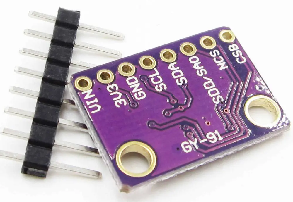
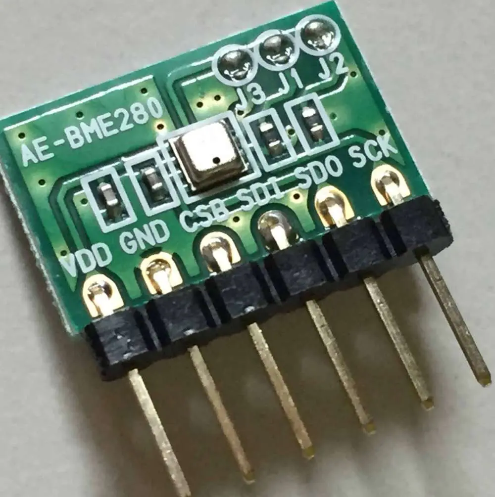
What is Grove – BME280 Environmental Sensor?

BME 280 can be referred to as an environmental sensor integrated by Bosch, which measures temperature, pressure, and humidity. By this, users will get a holistic and comprehensive measurement of their environment.
Furthermore, the sensor shows a quick response time to aid in supporting performance requirements, coupled with high accuracy. Asides from this, it is optimized for high resolution and low noise.
For bme280, we will be considering the environmental sensor, how BME280 is relevant to our world today, as well as other sensors related to the BME280.
This sensor is based on the Bosch BME28. This BME28 is known for its high-precision, low-cost, and its ability to support both SPI and I2C communication.
The Grove BME280 offers an accurate measurement of the environment’s humidity, temperature, and barometric pressure.
Due to its great accuracy during pressure measurement, and changes of pressure with altitude, it becomes easy to calculate its altitude with a meter accuracy of +1. This also makes it an accurate and precise altimeter.
Furthermore, there’s no need to be concerned about I2C collisions, because it offers both SPI and I2C interfaces. In order to make use of the SPI, just desolder its bonding pads, which are found on the back of the breakout board of the BME280. For I2C, its board also offers two I2C addresses, giving you the option of choosing whichever you want.
Also present are libraries that have high abstracts. This ensures that users can use the BME 280 to build their projects faster and quicker.
Specifications of the Grove – BME280 Environmental Sensor
- Accuracy of Humidity ±3%
- Weight G.W 10g
- Range of Temperature -40 to 85
- Accuracy of Air Pressure ±1.0 hPa
- Range of Air pressure 300 – 1100 hPa
- Dimensions 40mm x20mm x15mm
- Voltage Supply 5V or 3.3V
- Current Consumption 0.4 mA
- Accuracy of Temperature ±1
Grove Background
You may have asked what groove is all about. Grove can be described as the personal modular of Seeed. It is also its standard connector prototyping system.
For Grove to help in assembling electronics, Grove utilizes an approach called building block. In contrast to the solder or jumper based system, connecting, building, and experimenting it is easier. This ensures that the system of learning is easy for the hobbyists. You don’t have to worry because it doesn’t get to a point when it begins to dump down.
BME280 Applications
You may be asking where the BME280 sensor can be applied. As a result of its features and capabilities such as its SPI and I2C compatibility, the BME 280 sensor is great for any type of weather, as well as environmental sensing. Below are some of the applications of the BME280.
- Monitoring of fitness
- Control of home automation
- Forecast of weather
- Indoor or outdoor navigation
- GPS navigation enhancement
- All other projects requiring appropriate reading of the atmospheric pressure
BME280 use with Arduino
You can use the environmental sensor Grove-BME280 with different microcontrollers such as Arduino, LinkIt ONE, and Beaglebone. You can achieve this through SPI or I2C. For our example today, we will be explaining to you how to connect your Grove environmental sensor BM280 to the Arduino.
Step by Step Guide
Step One: Connect the BME280 sensor to touch the Grove Base Shield V2 I2C port. After that, plug or insert it to Seeeduino. However, if you lack a Grove Base Shield, the module can be connected directly to the Seeeduino
Step Two: Using a USB cable, connect Seeeduino to the PC
Step Three: Here is the software aspect of the tutorial. First of all, visit Github to download the example and library code.
Step Four: Create a brand new sketch for the Arduino and then paste some codes to it. You can also get access to the code directly just by following this path: File – Example – Barometer_Sensor – Barometer_Sensor
Step Five: This step requires that you upload this code gotten in step five into your Arduino
Step Six: Open the serial monitor in order to receive the data of the sensor, which includes humidity, altitude, value of barometric pressure, and temperature.
That’s all. In these six steps, running the BME280 sensor with Seeeduino becomes very easy. Now let’s consider another sensor related to the BME280, which is the bmp 280.
BMP280 vs BME280: What’s the Difference?
The BMP280 shares similarities with the BME280. Also, they also have a very similar parameter performance. This is why people usually get confused.
However, we will clarify both. BMP 280 can measure just the air pressure and temperature. However, the BME280 can only measure humidity coupled with air pressure and temperature.
Due to this difference, you will get the BMP280 at a much cheaper rate compared to the BME280.
Furthermore, the barometer sensor BMP280 can be seen as a much better development to the barometer sensor BMP180. Also, the environmental sensor BME280 adds the measurement of humidity to the BMP280.
Therefore, if you wish to get just the atmospheric pressure, we advise that you utilize the BMP280. However, if you wish to monitor your environment comprehensively, then we advise that you choose the BME280.
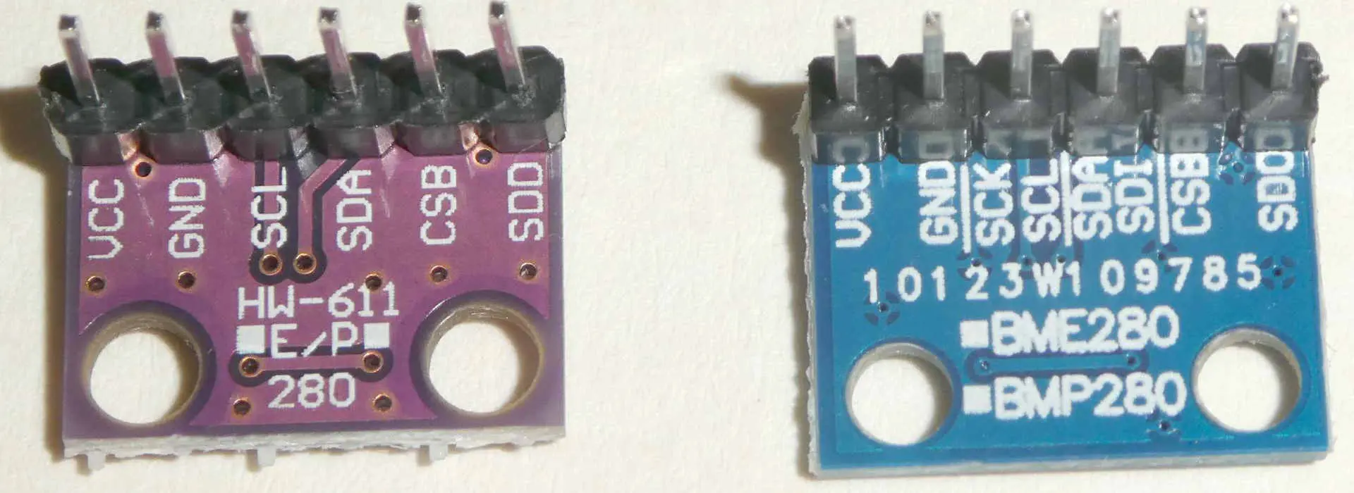
Other ways of detecting differences between bmp280 vs bme280 is by inspecting the pcb visually and by inspecting the package.
Inspecting the PCB visually
Also, you can see the difference between bmp280 vs bme280, just by inspecting the PCB visually. Checking the rear of the PCB, the one colored uniquely with the right printing is genuine. If the P text is covered with a black dot on its module and sold as a BME280, then it’s wrong. This is because the P text, which is hidden or covered, clearly indicates that it is BMP280. Original modules usually don’t come with a mark.
Inspecting the package
Finally, you can know the difference between bmp280 vs bme280 just by inspecting the package visually. If you check the datasheet of the BME280, you will see the markings for devices requiring mass production. This marking has to have ??? U? format. Here, the U signifies BME280. Now, the last ? you are seeing here is just a P, while the final two characters are supposed to be UP.
Comparing with the datasheet of BMP280, the format ought to be ??? K?. Here, the final “?” should be either W, N, U, P. Therefore, KW, KN, KU, KP are all devices of BMP280.
Conclusion
After reading through, you will come to understand that there are some differences between BMP280 vs BME280. If you decide to buy BME280 online, there’s a great chance that what you’ll get is the lesser BMP280. This is because some of these sellers simply don’t know what they are selling. Also, they simply don’t understand the difference between bmp280 vs bme280. Also, the break-out design of a PCB, which is shared between two different sensor types. Due to this reason, it could be frustrating when you buy these sensors. This is because sellers usually do this without getting caught.
To be sure of whatever you have ordered, you will have to spend some more money for modules from industries like Adafruit. Here, everything is properly controlled and labeled.