For PCB fabrication, we require PCB design file in Gerber RS-274X format (most preferred), *.PCB/DDB (Protel, inform your program version) format or *.BRD (Eagle) format.
Q2. Is there any Minimum quantity (MOQ) requirement for the PCB order?
Generally, there is no minimum order quantity (MOQ) requirement for the pcb order.
Q3. How quickly will I receive a response to my quotation request?
We guarantee a response to all quotation requests within 24 hours.
Q4. How do you keep costs affordable for PCB manufacturing services?
We utilize the latest and most efficient manufacturing technologies, ensuring both time and cost savings for your projects.
Q5. How many years of experience do you have in the PCB manufacturing industry?
With over 20 years of combined expertise, we specialize in delivering advanced PCB assembly and manufacturing services.
Q6. What is the smallest trace width and spacing you can manufacture?
Trace width: 3 mils Trace/line spacing: 3 mils When working with narrower traces, the tolerance becomes tighter, which can lead to over-etching. However, our controlled etching process ensures accurate trace widths are achieved.
We can use nearly all solder mask colors. The most frequently used options include Red, Green, Black, Blue, and White.
Q8. What surface finish options do you provide?
We offer a variety of surface finishes, including HASL, Lead-free HASL, ENIG, Immersion Silver, Immersion Tin, OSP, Soft Wire Bondable Gold, and Hard Gold.
Q9. What is the smallest hole size you can produce?
Mechanical drilling: 6 mils Laser drilling: 4 mils Including various hole sizes in a PCB design necessitates the use of additional drill bits during manufacturing, which can lead to higher costs and longer production times.
Q10. Does my board require impedance control and stack-up design?
Yes, we offer free impedance control calculations and stack-up design using industry-leading field solvers. Impedance control involves aligning PCB trace dimensions and placements with the substrate material’s properties to ensure signal strength remains within the desired range. By adhering to best design practices, many potential signal integrity issues can be prevented or minimized.
Q11. Can you manufacture a panel with different types of boards?
Yes, we can produce panels containing multiple board types. However, we will need to review your design files before providing a final confirmation.
Yes, we do. A peelable solder mask is used to protect specific areas of a PCB during the assembly process, particularly during wave soldering. It ensures that solder does not come into contact with the designated protected regions.
Q13. Can you produce flex boards?
Yes, we specialize in manufacturing both flexible and rigid-flex PCBs.
Q14. What electrical testing methods do you employ?
We utilize two primary testing methods: 1. Flying Probe 2. Test Fixture
Q15. Can you manufacture PCBs for high RF applications?
Yes, we are equipped to produce PCBs designed for high-frequency and RF applications.
Q19. Can you manufacture High-Density Interconnect (HDI) PCBs?
Yes, we are capable of producing HDI PCBs. For further details, please visit our PCB Fabrication page. HDI PCBs achieve greater circuit density compared to traditional PCBs by incorporating advanced features and technologies, including blind/buried vias, laser-drilled stacked micro-vias, via-in-pad techniques, and more.
Q20. Can you produce PCBs with castellation holes (plated half-holes on the PCB edge)?
Yes, we offer castellation hole services. We recommend using the largest hole size feasible for optimal results.
Q21. Do you offer V-scoring services?
Yes, we provide V-scoring for bare PCB orders as needed.
Q22. What factors influence PCB manufacturing costs?
1. Board quantity 2. PCB thickness 3. Number of layers 4. Copper weight 5. HDI features 6. Routing complexity 7. Impedance control requirements
Q23. Do you provide special milling or controlled-depth routing services?
Yes, we offer both controlled-depth routing and special milling.
Q24. What types of laminates do you use for PCB fabrication?
We utilize a wide range of laminates, including FR4, High TG FR4, Rogers, Arlon, Aluminum Base, Polyimide, Ceramic, Taconic, Megtron, and more.
Light Emitting Diodes (LEDs) have revolutionized the lighting industry, offering energy-efficient and long-lasting solutions for various applications. As technology advances, different types of LED configurations have emerged to cater to specific needs and preferences. This article will explore three popular options for LED PCBs: Surface Mount Device (SMD) LEDs, Chip on Board (COB) LEDs, and Direct on Board (DOB) LEDs. We’ll delve into their characteristics, advantages, disadvantages, and applications to help you make an informed decision for your lighting projects.
Understanding LED PCBs
Before we dive into the specifics of SMD, COB, and DOB LEDs, it’s essential to understand the role of Printed Circuit Boards (PCBs) in LED technology. PCBs serve as the foundation for mounting and connecting electronic components, including LEDs. They provide mechanical support, electrical connections, and heat dissipation, which are crucial for the performance and longevity of LED systems.
SMD LED: Surface Mount Device
What is SMD LED?
Surface Mount Device (SMD) LEDs are compact, pre-packaged LED chips that can be directly mounted onto the surface of a PCB. They are widely used in various lighting applications due to their versatility and ease of integration.
Characteristics of SMD LEDs
Size and Package: SMD LEDs come in various package sizes, typically ranging from 2835 (2.8mm x 3.5mm) to 5050 (5.0mm x 5.0mm).
Components: Each SMD LED package contains one or more LED chips, a reflector cup, and wire bonding.
Color Options: Available in a wide range of colors, including white, RGB, and multi-color configurations.
Luminous Efficacy: Typically ranges from 100 to 160 lumens per watt, depending on the specific model and manufacturer.
Advantages of SMD LEDs
Versatility: Can be used in various applications, from small electronics to large-scale lighting projects.
Color Mixing: Easy to create multi-color or tunable white light solutions.
Heat Dissipation: Generally good heat dissipation due to the spread-out nature of individual LEDs.
Customization: Allows for flexible design and customization of light output and distribution.
Disadvantages of SMD LEDs
Individual Mounting: Each LED must be individually placed on the PCB, which can be time-consuming for large-scale production.
Potential for Non-Uniform Light: If not properly designed, may result in visible individual light sources or hot spots.
More Components: Requires more components compared to COB or DOB LEDs, potentially increasing the risk of failure points.
Chip on Board (COB) LED technology involves mounting multiple LED chips directly onto a substrate to form a single module. This results in a more compact and powerful light source compared to individual SMD LEDs.
Characteristics of COB LEDs
Size and Package: COB LEDs are typically larger than SMD LEDs, with sizes ranging from 9mm to 30mm or more.
Components: Multiple LED chips are mounted directly on a substrate and covered with a layer of phosphor (for white light).
Color Options: Primarily available in white light with various color temperatures, though RGB options exist.
Luminous Efficacy: Generally higher than SMD LEDs, ranging from 130 to 200 lumens per watt.
Advantages of COB LEDs
High Lumen Density: Produces a large amount of light from a small area.
Uniform Light Output: Creates a more even light distribution without visible individual light sources.
Improved Thermal Management: Better heat dissipation due to direct mounting on the substrate.
Simplified Manufacturing: Easier to assemble and requires fewer components than multiple SMD LEDs.
Disadvantages of COB LEDs
Limited Color Options: Primarily available in white light, with fewer multi-color options compared to SMD LEDs.
Less Flexibility in Design: The fixed nature of the COB module limits customization options.
Higher Initial Cost: Generally more expensive per unit compared to SMD LEDs.
Potential for Glare: The high lumen density can cause glare if not properly diffused or directed.
Applications of COB LEDs
High-bay lighting for warehouses and industrial spaces
Spotlights and track lighting
Street and area lighting
Automotive headlights
DOB LED: Direct on Board
What is DOB LED?
Direct on Board (DOB) LED technology is the latest innovation in LED lighting. It involves mounting LED chips directly onto the main PCB without the need for a separate substrate or package.
Characteristics of DOB LEDs
Size and Package: DOB LEDs are integrated directly into the PCB, allowing for very thin and compact designs.
Components: LED chips are mounted directly on the main PCB along with other necessary components.
Color Options: Available in various color temperatures of white light, with some RGB options.
Luminous Efficacy: Comparable to or slightly higher than COB LEDs, ranging from 150 to 220 lumens per watt.
Advantages of DOB LEDs
Simplified Manufacturing: Eliminates the need for a separate LED package or module, streamlining production.
Improved Thermal Performance: Direct contact with the PCB allows for better heat dissipation.
Cost-Effective: Reduces overall production costs by eliminating intermediate components and assembly steps.
Ultra-Thin Designs: Enables the creation of extremely thin and lightweight lighting fixtures.
Disadvantages of DOB LEDs
Limited Availability: As a newer technology, there may be fewer suppliers and options compared to SMD or COB LEDs.
Specialized Equipment: May require specialized manufacturing equipment and processes.
Repair Challenges: In case of LED failure, the entire PCB may need to be replaced.
Design Constraints: The integration of LEDs directly on the PCB may limit some design flexibility.
Applications of DOB LEDs
Flat panel lights
Ultra-thin downlights
Linear lighting fixtures
Automotive interior lighting
Comparison of SMD, COB, and DOB LEDs
To better understand the differences between these three LED PCB options, let’s compare them across various parameters:
Parameter
SMD LED
COB LED
DOB LED
Size
Small, individual packages
Larger, single module
Integrated into PCB
Lumen Density
Moderate
High
High
Color Options
Wide range, including RGB
Primarily white, limited RGB
Primarily white, some RGB
Heat Dissipation
Good
Better
Best
Cost
Low to moderate
Moderate to high
Moderate
Manufacturing Complexity
Moderate
Low
Lowest
Customization
High
Limited
Moderate
Luminous Efficacy (lm/W)
100-160
130-200
150-220
Glare Potential
Low
High
Moderate
Repair/Replacement
Easy
Moderate
Difficult
Choosing the Right LED PCB Option
When selecting between SMD, COB, and DOB LEDs for your project, consider the following factors:
Application: Determine the specific lighting requirements for your project.
Light Output: Consider the desired lumen output and distribution pattern.
Color Requirements: Decide if you need white light, specific color temperatures, or RGB capabilities.
Space Constraints: Evaluate the available space for the lighting fixture.
Thermal Management: Assess the heat dissipation needs of your application.
Cost Considerations: Balance initial costs with long-term energy efficiency and maintenance.
Manufacturing Capabilities: Consider your production volume and available manufacturing processes.
Application-Specific Recommendations
Application
Recommended LED Type
Reasoning
LED Strips
SMD LED
Flexibility and color options
High-Bay Lighting
COB LED
High lumen output and uniform distribution
Ultra-Thin Panels
DOB LED
Compact design and efficient heat management
Automotive Lighting
SMD or COB LED
Versatility for different automotive applications
Outdoor Lighting
COB or DOB LED
High efficiency and good thermal management
Decorative Lighting
SMD LED
Wide color range and design flexibility
Future Trends in LED PCB Technology
As LED technology continues to evolve, we can expect to see further improvements in efficiency, cost-effectiveness, and application-specific solutions. Some potential trends include:
Increased DOB LED Adoption: As manufacturing processes improve, DOB LEDs may become more prevalent across various lighting applications.
Hybrid Solutions: Combinations of different LED types on a single PCB to optimize performance for specific use cases.
Advanced Thermal Management: Development of new materials and designs to further improve heat dissipation.
Smart Integration: Incorporation of sensors and control systems directly into LED PCBs for improved functionality and energy efficiency.
Micro-LED Technology: Advancements in extremely small LED chips may lead to new possibilities in display and lighting applications.
Conclusion
SMD, COB, and DOB LEDs each offer unique advantages and are suited for different applications in the world of lighting. SMD LEDs provide versatility and color options, COB LEDs offer high lumen density and uniform output, while DOB LEDs excel in thermal management and manufacturing simplicity. By understanding the characteristics, pros, and cons of each option, you can make an informed decision for your specific lighting project. As LED technology continues to advance, we can expect even more efficient and innovative solutions to emerge, further revolutionizing the lighting industry.
Frequently Asked Questions (FAQ)
1. Which LED type is best for energy efficiency?
While all three types are energy-efficient, DOB LEDs generally offer the highest luminous efficacy, followed closely by COB LEDs. However, the overall energy efficiency of a lighting system depends on various factors, including the specific product, driver efficiency, and thermal management.
2. Can I replace SMD LEDs with COB or DOB LEDs in existing fixtures?
In most cases, it’s not a straightforward replacement due to differences in size, power requirements, and heat dissipation. It’s usually best to design fixtures specifically for the chosen LED type. However, some modular systems may allow for easier upgrades or replacements.
3. Are COB LEDs always better than SMD LEDs for high-power applications?
While COB LEDs are often preferred for high-power applications due to their high lumen density and better thermal management, SMD LEDs can still be suitable in some cases. The choice depends on factors such as the specific power requirements, desired beam angle, and color mixing needs.
4. How do I determine which LED type is best for my project?
Consider factors such as the required light output, color options, space constraints, thermal management needs, and budget. It’s often helpful to consult with lighting designers or engineers who can provide expertise based on your specific project requirements.
5. Are DOB LEDs more expensive than SMD or COB LEDs?
Initially, DOB LEDs may have a higher cost due to the newer technology and potentially specialized manufacturing processes. However, they can be more cost-effective in the long run due to simplified manufacturing, improved thermal management, and potentially longer lifespans. As the technology becomes more widespread, costs are likely to decrease.
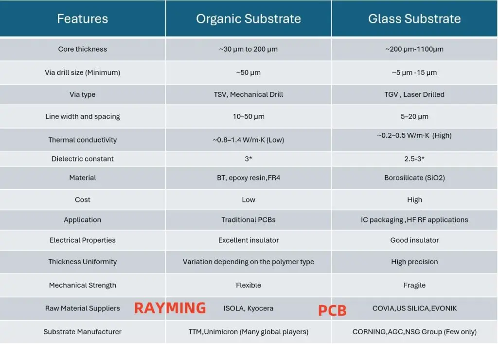
In the realm of electronics and semiconductor manufacturing, the choice of substrate material plays a pivotal role in determining the performance, reliability, and cost-effectiveness of the final product. Two prominent types of substrates used in various applications are organic core substrates and glass core substrates. Each type has its unique set of properties, advantages, and limitations, making them suitable for different applications. This article delves into a comprehensive comparison between organic core and glass core substrates based on the provided data, covering aspects such as core thickness, via drill size, thermal conductivity, dielectric constant, material composition, cost, applications, electrical properties, thickness uniformity, mechanical strength, and raw material suppliers.
Core Thickness
Organic Core Substrate:
Range: ~30μm to 200μm
Characteristics: Organic core substrates typically have a thinner core compared to glass core substrates. This thinness allows for greater flexibility and lighter weight, which is advantageous in applications where space and weight are critical factors.
Glass Core Substrate:
Range: ~200μm to 1100μm
Characteristics: Glass core substrates are generally thicker, providing better mechanical stability and rigidity. This makes them suitable for applications requiring high precision and durability, such as in IC packaging and high-frequency RF applications.
Via Drill Size
Organic Core Substrate:
Minimum Size: ~50μm
Via Type: TSV (Through-Silicon Via), Mechanical Drill
Characteristics: The larger via drill size in organic core substrates facilitates easier manufacturing processes and is cost-effective. However, it may limit the density of interconnections, which can be a drawback in high-density applications.
Glass Core Substrate:
Minimum Size: ~5μm to 15μm
Via Type: TGV (Through-Glass Via), Laser Drilled
Characteristics: The significantly smaller via drill size in glass core substrates allows for higher interconnection density, which is crucial for advanced packaging and high-frequency applications. The precision of laser drilling also ensures high-quality vias with minimal defects.
Thermal Conductivity
Organic Core Substrate:
Range: ~0.8-1.4 W/m-K (Low)
Characteristics: Organic materials generally have lower thermal conductivity, which can lead to heat buildup in high-power applications. This necessitates additional thermal management solutions, such as heat sinks or thermal vias.
Glass Core Substrate:
Range: ~0.2-0.5 W/m-K (High)
Characteristics: Glass core substrates exhibit higher thermal conductivity, making them more efficient at dissipating heat. This property is particularly beneficial in high-power and high-frequency applications where thermal management is critical.
Dielectric Constant
Organic Core Substrate:
Value: ~3
Characteristics: The dielectric constant of organic core substrates is relatively low, which is advantageous for high-speed signal transmission. Lower dielectric constants reduce signal loss and improve the overall performance of high-frequency circuits.
Glass Core Substrate:
Value: ~2.5-3
Characteristics: Glass core substrates also have a low dielectric constant, comparable to organic core substrates. This makes them suitable for high-frequency applications where signal integrity is paramount.
Characteristics: Organic core substrates are composed of polymer-based materials, which are lightweight and flexible. These materials are cost-effective and widely available, making them a popular choice for traditional PCBs.
Glass Core Substrate:
Materials: Borosilicate (SiO2)
Characteristics: Glass core substrates are made from borosilicate glass, which offers excellent mechanical and thermal properties. However, the material is more expensive and less flexible compared to organic materials.
Cost
Organic Core Substrate:
Cost: Low
Characteristics: The use of polymer-based materials and simpler manufacturing processes contribute to the lower cost of organic core substrates. This makes them an economical choice for a wide range of applications, especially in consumer electronics.
Glass Core Substrate:
Cost: High
Characteristics: The higher cost of glass core substrates is attributed to the expensive raw materials and the complex manufacturing processes involved, such as laser drilling for vias. This makes them more suitable for high-end applications where performance is critical.
Applications
Organic Core Substrate:
Applications: Traditional PCBs
Characteristics: Organic core substrates are widely used in traditional printed circuit boards (PCBs) due to their cost-effectiveness and flexibility. They are suitable for a broad range of consumer electronics, including smartphones, laptops, and home appliances.
Glass Core Substrate:
Applications: IC Packaging, High-Frequency RF Applications
Characteristics: Glass core substrates are preferred in advanced packaging and high-frequency RF applications due to their superior thermal and electrical properties. They are commonly used in high-performance computing, telecommunications, and aerospace industries.
Electrical Properties
Organic Core Substrate:
Properties: Excellent insulator
Characteristics: Organic core substrates provide excellent electrical insulation, which is crucial for preventing short circuits and ensuring reliable performance in electronic devices.
Glass Core Substrate:
Properties: Good insulator
Characteristics: While glass core substrates also offer good electrical insulation, their primary advantage lies in their thermal and mechanical properties, which are more critical in high-performance applications.
Thickness Uniformity
Organic Core Substrate:
Uniformity: Variation depending on the polymer type
Characteristics: The thickness uniformity of organic core substrates can vary based on the type of polymer used. This variability can affect the consistency of the substrate’s performance, especially in high-precision applications.
Glass Core Substrate:
Uniformity: High precision
Characteristics: Glass core substrates exhibit high precision in thickness uniformity, which is essential for applications requiring consistent performance and reliability, such as in IC packaging.
Mechanical Strength
Organic Core Substrate:
Strength: Flexible
Characteristics: The flexibility of organic core substrates makes them suitable for applications where the substrate may be subjected to bending or flexing, such as in flexible electronics.
Glass Core Substrate:
Strength: Fragile
Characteristics: Glass core substrates are more rigid and fragile compared to organic core substrates. While this fragility can be a limitation in some applications, it provides the necessary mechanical stability for high-precision applications.
Raw Material Suppliers
Organic Core Substrate:
Suppliers: ISOLA, Kyocera
Characteristics: The raw materials for organic core substrates are supplied by a wide range of global players, ensuring a steady supply chain and competitive pricing.
Glass Core Substrate:
Suppliers: COVIA, US SILICA, EVONIK
Characteristics: The raw materials for glass core substrates are supplied by a limited number of specialized manufacturers, which can impact the availability and cost of these substrates.
Substrate Manufacturers
Organic Core Substrate:
Manufacturers: TTM, Unimicron (Many global players)
Characteristics: The manufacturing of organic core substrates is carried out by numerous global players, leading to a competitive market and a wide range of options for consumers.
Glass Core Substrate:
Manufacturers: CORNING, AGC, NsG Group (Few only)
Characteristics: The manufacturing of glass core substrates is dominated by a few specialized companies, which can limit the availability and increase the cost of these substrates.
Conclusion
In summary, the choice between organic core and glass core substrates depends on the specific requirements of the application. Organic core substrates offer cost-effectiveness, flexibility, and excellent electrical insulation, making them suitable for traditional PCBs and consumer electronics. On the other hand, glass core substrates provide superior thermal conductivity, high precision, and mechanical stability, making them ideal for advanced packaging and high-frequency RF applications. Understanding the distinct properties and advantages of each substrate type is crucial for selecting the appropriate material to meet the performance and reliability needs of the intended application.
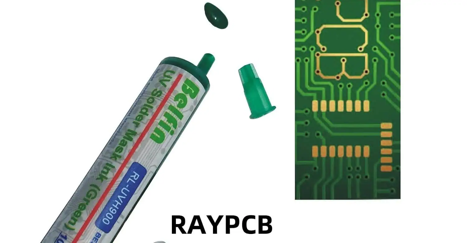
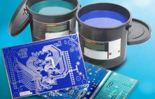
Applying a solder mask to a Printed Circuit Board (PCB) is a crucial step in the PCB manufacturing process. The solder mask protects the copper traces from oxidation, prevents solder bridges, and enhances the overall durability of the board. While professional PCB manufacturers use advanced equipment to apply solder masks, it is possible to apply a UV solder mask at home with the right tools and techniques. This guide provides a comprehensive, step-by-step process for applying UV solder mask to your PCB board at home.
1. Understanding UV Solder Mask
1.1 What is UV Solder Mask?
UV solder mask is a type of solder resist that cures (hardens) when exposed to ultraviolet (UV) light. It is typically supplied as a liquid or film and is applied to the PCB to cover the copper traces, leaving only the pads exposed for soldering.
1.2 Benefits of UV Solder Mask
Protection: Protects copper traces from oxidation and environmental damage.
Insulation: Prevents electrical shorts by insulating conductive traces.
Solder Control: Prevents solder from bridging between closely spaced pads.
Aesthetic Appeal: Provides a professional finish to the PCB.
1.3 Tools and Materials Required
To apply UV solder mask at home, you will need the following tools and materials:
UV Solder Mask Liquid or Film: Available in various colors (green, blue, red, etc.).
UV Light Source: A UV lamp or UV curing chamber.
Squeegee or Brush: For spreading the solder mask evenly.
Photo Film or Transparency Sheet: For creating a solder mask stencil.
PCB Cleaning Supplies: Isopropyl alcohol, lint-free cloth, and a brush.
Plastic Container: For mixing and storing the solder mask.
Protective Gear: Gloves, safety glasses, and a mask to protect against fumes.
2. Step-by-Step Guide to Applying UV Solder Mask
2.1 Step 1: Prepare the PCB
2.1.1 Clean the PCB
Before applying the solder mask, ensure that the PCB is clean and free of dust, grease, and oxidation. Follow these steps:
Wipe the PCB with a lint-free cloth soaked in isopropyl alcohol.
Use a soft brush to remove any debris from the traces and pads.
Allow the PCB to dry completely.
2.1.2 Inspect the PCB
Inspect the PCB for any defects, such as scratches or exposed copper. Repair any issues before proceeding.
2.2 Step 2: Create the Solder Mask Stencil
2.2.1 Design the Stencil
Using PCB design software (e.g., KiCad, Eagle, or Altium), create a solder mask layer that exposes only the pads and vias. Export this layer as a high-resolution image or PDF.
2.2.2 Print the Stencil
Print the solder mask layer onto a photo film or transparency sheet using a laser printer. Ensure that the print is dark and opaque to block UV light effectively.
2.3 Step 3: Apply the UV Solder Mask
2.3.1 Mix the Solder Mask (if required)
If using a two-part UV solder mask, mix the components according to the manufacturer’s instructions. Stir gently to avoid introducing air bubbles.
2.3.2 Apply the Solder Mask
There are two main methods for applying UV solder mask: liquid application and film application.
Liquid Application Method:
Pour a small amount of UV solder mask liquid onto the PCB.
Use a squeegee or brush to spread the liquid evenly over the entire surface.
Ensure that the solder mask covers all the traces while leaving the pads exposed.
Film Application Method:
Cut a piece of UV solder mask film slightly larger than the PCB.
Peel off the protective layer and carefully place the film onto the PCB.
Use a roller or squeegee to remove air bubbles and ensure proper adhesion.
2.4 Step 4: Align and Expose the Stencil
2.4.1 Align the Stencil
Place the printed photo film or transparency sheet over the PCB, ensuring that the pads and vias align perfectly with the openings in the stencil.
2.4.2 Expose to UV Light
Place the PCB and stencil under the UV light source.
Expose the PCB to UV light for the recommended duration (usually 1-5 minutes, depending on the solder mask and UV light intensity).
Rotate the PCB if necessary to ensure even exposure.
2.5 Step 5: Develop the Solder Mask
2.5.1 Remove the Stencil
After exposure, carefully remove the photo film or transparency sheet from the PCB.
2.5.2 Rinse the PCB
Rinse the PCB with water or a developer solution (as specified by the solder mask manufacturer) to remove the uncured solder mask. Use a soft brush to gently scrub the surface.
2.5.3 Dry the PCB
Allow the PCB to dry completely. You can use compressed air or a lint-free cloth to speed up the drying process.
2.6 Step 6: Cure the Solder Mask
2.6.1 Final UV Exposure
Place the PCB under the UV light source again for a final cure. This step ensures that the solder mask is fully hardened and durable.
2.6.2 Inspect the PCB
Inspect the PCB for any defects, such as incomplete coverage or misaligned pads. Touch up any areas if necessary.
3. Tips for Success
3.1 Work in a Clean Environment
Dust and debris can affect the quality of the solder mask application. Work in a clean, well-ventilated area to minimize contamination.
3.2 Use High-Quality Materials
Invest in high-quality UV solder mask and photo film to ensure the best results. Cheap materials may lead to poor adhesion or incomplete curing.
3.3 Practice on Scrap PCBs
If you are new to applying solder masks, practice on scrap PCBs before working on your final project. This will help you refine your technique and avoid mistakes.
3.4 Follow Manufacturer Instructions
Always follow the manufacturer’s instructions for mixing, applying, and curing the solder mask. Different products may have specific requirements.
Solution: Apply a thicker layer of solder mask and use a squeegee to spread it evenly.
4.2 Solder Mask Peeling
Cause: Poor adhesion due to contamination or improper curing.
Solution: Clean the PCB thoroughly before application and ensure proper UV exposure.
4.3 Misaligned Pads
Cause: Incorrect alignment of the stencil.
Solution: Double-check the alignment before exposing the PCB to UV light.
4.4 Air Bubbles
Cause: Trapped air during application.
Solution: Use a roller or squeegee to remove air bubbles before curing.
5. Advantages of Applying UV Solder Mask at Home
5.1 Cost-Effective
Applying solder mask at home can save money compared to outsourcing the process to a professional PCB manufacturer.
5.2 Customization
You have full control over the design and application process, allowing for greater customization.
5.3 Learning Experience
The process provides valuable hands-on experience and a deeper understanding of PCB manufacturing.
Conclusion
Applying UV solder mask to your PCB board at home is a rewarding and cost-effective way to enhance the durability and functionality of your PCBs. By following the step-by-step guide outlined above, you can achieve professional-quality results with the right tools and techniques. Whether you are a hobbyist or a professional, mastering this skill will enable you to create high-quality PCBs for a wide range of applications. With practice and attention to detail, you can confidently apply UV solder mask to your PCB projects at home.
In the world of Printed Circuit Board (PCB) manufacturing, the solder mask plays a crucial role in ensuring the reliability and functionality of the final product. Among the various features of a solder mask, the solder mask dam is a critical element that often goes unnoticed but is essential for preventing solder-related defects. This article provides a comprehensive overview of what a solder mask dam is, its purpose, design considerations, and its importance in PCB manufacturing.
1. Understanding Solder Mask
Before diving into the specifics of a solder mask dam, it is essential to understand the solder mask itself.
1.1 What is Solder Mask?
Solder mask, also known as solder resist, is a thin, protective layer applied to the copper traces of a PCB. It is typically made of a polymer material that is resistant to heat, chemicals, and environmental factors. The primary functions of the solder mask include:
Protection: It protects the copper traces from oxidation, corrosion, and environmental damage.
Insulation: It prevents electrical shorts by insulating the conductive traces.
Solder Control: It prevents solder from bridging between closely spaced pads during the soldering process.
1.2 Types of Solder Mask
Solder masks come in various types, including:
Liquid Photoimageable Solder Mask (LPSM): Applied as a liquid and cured using UV light.
Dry Film Solder Mask: Applied as a dry film and laminated onto the PCB.
Epoxy-Based Solder Mask: Typically used for simpler designs and less demanding applications.
2. What is a Solder Mask Dam?
2.1 Definition
A solder mask dam is a small, raised barrier of solder mask material that is intentionally left between two adjacent pads or features on a PCB. Its primary purpose is to prevent solder from flowing between these pads during the soldering process, thereby avoiding solder bridging and short circuits.
2.2 Purpose of a Solder Mask Dam
The solder mask dam serves several critical functions:
Preventing Solder Bridging: By creating a physical barrier between adjacent pads, the solder mask dam prevents molten solder from forming unintended connections (bridges) during reflow soldering or wave soldering.
Improving Solder Joint Quality: It ensures that solder is confined to the intended pads, resulting in better solder joint formation and reliability.
Enhancing Electrical Isolation: The dam provides additional insulation between conductive traces, reducing the risk of electrical shorts.
Facilitating Fine-Pitch Components: For components with fine-pitch leads (e.g., BGAs, QFPs), solder mask dams are essential for maintaining proper spacing and preventing defects.
3. Design and Implementation of Solder Mask Dams
3.1 Design Considerations
Designing an effective solder mask dam requires careful consideration of several factors:
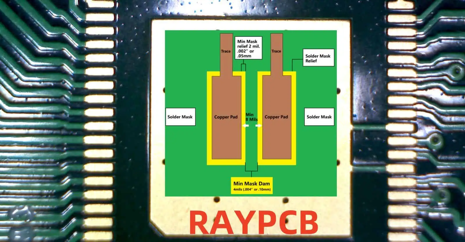
3.1.1 Width and Height
The width of the solder mask dam must be sufficient to prevent solder from bridging but not so wide that it encroaches on the pad area.
The height of the dam is determined by the thickness of the solder mask layer, which is typically between 0.5 mils (0.013 mm) and 2 mils (0.05 mm).
3.1.2 Clearance
Adequate clearance must be maintained between the solder mask dam and the pad edges to ensure proper solder wetting and joint formation.
The clearance is often defined by the PCB manufacturer’s design rules and depends on the soldering process used.
3.1.3 Material Properties
The solder mask material must have good thermal and chemical resistance to withstand the soldering process without degrading.
The implementation of solder mask dams involves the following steps:
Design Phase:
The solder mask dam is defined in the PCB design files (e.g., Gerber files) as part of the solder mask layer.
The design software automatically generates the dam based on the specified clearance rules.
Application Phase:
The solder mask is applied to the PCB using methods such as screen printing, curtain coating, or spray coating.
The areas where the dam is required are masked off during the application process.
Curing Phase:
The solder mask is cured using UV light or heat to harden the material and ensure proper adhesion.
Inspection Phase:
The solder mask dam is inspected for defects such as insufficient height, uneven coverage, or misalignment.
4. Importance of Solder Mask Dams in PCB Manufacturing
4.1 Preventing Solder Bridging
Solder bridging is one of the most common defects in PCB assembly. It occurs when molten solder forms unintended connections between adjacent pads or traces. Solder mask dams act as physical barriers to prevent this issue, especially in fine-pitch components where the risk of bridging is high.
4.2 Enhancing Reliability
By preventing solder bridging and ensuring proper solder joint formation, solder mask dams contribute to the overall reliability of the PCB. Reliable solder joints are essential for the long-term performance of electronic devices.
4.3 Facilitating Miniaturization
As electronic devices become smaller and more complex, the demand for fine-pitch components and high-density PCBs has increased. Solder mask dams enable the use of these components by maintaining proper spacing and preventing defects.
4.4 Reducing Rework and Costs
Defects such as solder bridging can lead to costly rework and delays in production. By incorporating solder mask dams, manufacturers can reduce the likelihood of such defects, saving time and money.
5. Challenges and Solutions in Solder Mask Dam Design
5.1 Challenges
5.1.1 Insufficient Dam Height
If the solder mask dam is too low, it may not effectively prevent solder bridging. This can occur due to improper application or curing of the solder mask.
5.1.2 Misalignment
Misalignment of the solder mask dam can result in inadequate coverage or encroachment on the pad area, leading to soldering defects.
5.1.3 Material Degradation
Exposure to high temperatures or harsh chemicals during the soldering process can cause the solder mask material to degrade, reducing the effectiveness of the dam.
5.2 Solutions
5.2.1 Optimizing Design Rules
Ensuring that the solder mask dam design adheres to the manufacturer’s guidelines and industry standards can help avoid issues such as insufficient height or misalignment.
5.2.2 Using High-Quality Materials
Selecting solder mask materials with excellent thermal and chemical resistance can prevent degradation and ensure the durability of the dam.
5.2.3 Advanced Manufacturing Techniques
Using advanced application and curing techniques, such as laser direct imaging (LDI) for precise alignment, can improve the quality and consistency of solder mask dams.
6. Applications of Solder Mask Dams
6.1 Fine-Pitch Components
Solder mask dams are essential for fine-pitch components such as Ball Grid Arrays (BGAs), Quad Flat Packages (QFPs), and Chip-Scale Packages (CSPs), where the risk of solder bridging is high.
6.2 High-Density Interconnect (HDI) PCBs
HDI PCBs, which feature densely packed traces and components, rely on solder mask dams to maintain proper spacing and prevent defects.
6.3 High-Reliability Applications
In industries such as aerospace, automotive, and medical devices, where reliability is critical, solder mask dams play a vital role in ensuring the performance and longevity of PCBs.
7. Future Trends in Solder Mask Technology
7.1 Advanced Materials
The development of new solder mask materials with enhanced thermal, chemical, and mechanical properties will improve the performance of solder mask dams.
7.2 Precision Manufacturing
Advancements in manufacturing techniques, such as 3D printing and laser-based processes, will enable the creation of more precise and reliable solder mask dams.
The solder mask dam is a small but critical feature in PCB manufacturing that plays a significant role in preventing solder bridging, enhancing reliability, and facilitating the use of fine-pitch components. By understanding its purpose, design considerations, and challenges, manufacturers can optimize their processes to produce high-quality, reliable PCBs. As technology continues to evolve, advancements in materials and manufacturing techniques will further improve the effectiveness of solder mask dams, ensuring their continued importance in the electronics industry.
Solder mask bridges are critical components in PCB manufacturing that prevent solder from creating unwanted connections between adjacent pads and traces. When these protective barriers break off, they can cause serious issues including short circuits, reduced reliability, and compromised performance. This comprehensive guide explores why solder mask bridges fail and provides practical solutions to prevent this costly problem.
What Are Solder Mask Bridges and Why Do They Matter?
Understanding Solder Mask
Solder mask (also called solder resist) is a protective polymer layer applied over copper traces on printed circuit boards. This thin coating serves three essential functions:
Protection: Shields copper traces from oxidation and environmental damage Insulation: Prevents electrical shorts by insulating conductive pathways Solder Control: Stops solder from bridging between closely spaced components during assembly
The Critical Role of Solder Mask Bridges
Solder mask bridges are the narrow sections of solder mask that span the gaps between adjacent pads or traces. These bridges act as physical barriers during the soldering process, ensuring solder flows only where intended. When bridges break off, the protective barrier is compromised, leading to potential manufacturing defects and long-term reliability issues.
Top 5 Causes of Solder Mask Bridge Failure
1. Poor Application Process
Inadequate Coverage When solder mask isn’t applied evenly or with sufficient thickness, weak bridges form that cannot withstand normal handling. Thin or uneven coverage creates stress points that are prone to cracking and detachment.
Improper Curing The curing process determines the mechanical strength of the solder mask. Incorrect temperature, insufficient duration, or poor environmental control during curing results in weak material properties and reduced adhesion.
2. Mechanical Stress Damage
Handling and Assembly Stress Excessive force during component placement, rough handling during transportation, or improper storage practices can cause immediate bridge failure. Even normal assembly processes can stress poorly formed bridges beyond their breaking point.
Thermal Cycling Effects Repeated heating and cooling cycles cause expansion and contraction of PCB materials. Over time, this thermal stress accumulates and can cause solder mask bridges to crack and detach, especially when the material lacks sufficient flexibility.
3. Material Quality Issues
Substandard Solder Mask Materials Low-quality solder mask materials may not meet required specifications for adhesion, flexibility, or thermal resistance. These materials are more likely to form weak bridges that fail under normal operating conditions.
Material Incompatibility Incompatible combinations of solder mask, PCB substrate, or other manufacturing materials can lead to poor adhesion and weak interface bonds. This incompatibility often becomes apparent only after thermal or mechanical stress testing.
4. Design-Related Problems
Insufficient Clearance When the space between pads or traces is too narrow, there isn’t enough solder mask material to form a robust bridge. These thin bridges lack the structural integrity needed to withstand manufacturing and operating stresses.
Stress Concentration Points Sharp corners, acute angles, and abrupt geometry changes in PCB designs create stress concentration points in the solder mask. These areas are particularly vulnerable to crack initiation and propagation.
5. Environmental Factors
Moisture and Humidity Exposure Prolonged exposure to moisture can degrade solder mask materials, reducing their mechanical properties and adhesion strength. This degradation makes bridges more susceptible to breaking off during handling or operation.
Chemical Degradation Harsh chemicals used in manufacturing processes or present in operating environments can attack solder mask materials, weakening their structure and reducing their ability to form durable bridges.
Serious Consequences of Bridge Failure
Immediate Manufacturing Issues
Solder Bridging: Without protective bridges, solder can flow between adjacent pads, creating unintended electrical connections and short circuits.
Assembly Defects: Bridge failure during assembly can lead to immediate rework requirements, increasing production time and costs.
Long-Term Reliability Problems
Reduced Protection: Exposed copper traces become vulnerable to oxidation and environmental damage without proper solder mask coverage.
Performance Degradation: Short circuits and compromised insulation can cause signal integrity issues and circuit malfunction.
Increased Failure Rates: Products with compromised solder mask are more likely to fail in the field, leading to warranty claims and reputation damage.
Proven Prevention Strategies
Optimizing Application Processes
Ensure Adequate Coverage Implement automated application methods like screen printing or curtain coating to achieve consistent, adequate solder mask thickness. Establish minimum thickness requirements and verify coverage through regular quality checks.
Perfect the Curing Process Follow manufacturer specifications exactly for curing temperature, time, and atmospheric conditions. Implement process monitoring to ensure consistent curing parameters across all production runs.
Minimizing Mechanical Stress
Implement Careful Handling Procedures Train personnel in proper PCB handling techniques, use appropriate fixtures and tooling, and establish controlled storage and transportation procedures to minimize mechanical damage.
Control Thermal Exposure Manage temperature profiles during soldering and avoid excessive thermal cycling during manufacturing. Select solder mask materials with appropriate thermal properties for the intended application.
Material Selection and Quality Control
Choose High-Quality Materials Source solder mask materials from reputable suppliers with proven track records. Verify that materials meet all relevant specifications and industry standards before use.
Ensure Material Compatibility Conduct compatibility testing between solder mask, substrate, and other materials used in the manufacturing process. Document approved material combinations and maintain consistency in sourcing.
Design Optimization
Provide Adequate Clearances Design with sufficient space between pads and traces to allow proper solder mask bridge formation. Follow IPC guidelines for minimum solder mask clearances based on trace spacing and manufacturing capabilities.
Eliminate Stress Concentrations Use rounded corners and smooth transitions in PCB layouts. Avoid sharp angles and abrupt geometry changes that can create stress concentration points in the solder mask.
Environmental Control
Manage Moisture and Humidity Implement controlled storage environments with appropriate humidity levels. Use desiccants and humidity monitoring to maintain optimal conditions throughout the manufacturing process.
Minimize Chemical Exposure Select chemical-resistant solder mask materials for harsh environments and implement proper chemical handling procedures to prevent material degradation.
Quality Control and Testing
Inspection Methods
Implement comprehensive inspection procedures including visual examination, adhesion testing, and thermal cycling tests to identify potential bridge weakness before assembly.
Process Monitoring
Establish real-time monitoring of critical process parameters including solder mask thickness, curing temperature, and humidity levels to ensure consistent quality.
Statistical Process Control
Use statistical methods to track bridge failure rates and identify process trends that may indicate developing quality issues.
Frequently Asked Questions (FAQ)
What is a solder mask bridge?
A solder mask bridge is the portion of solder mask material that spans the gap between adjacent pads or traces on a PCB. It acts as a physical barrier to prevent solder from creating unwanted connections during assembly.
Why do solder mask bridges break off?
Common causes include poor application processes (inadequate coverage or improper curing), mechanical stress from handling or thermal cycling, low-quality materials, design flaws like insufficient clearance, and environmental factors such as moisture or chemical exposure.
How can I tell if solder mask bridges are failing?
Look for visible cracks or missing sections of solder mask between pads, solder bridging during assembly, increased rework rates, or field failures related to short circuits. Regular quality inspections can help identify issues early.
What’s the minimum clearance needed for reliable solder mask bridges?
Minimum clearance depends on your manufacturing capabilities and design requirements, but typically ranges from 0.1mm to 0.15mm (4-6 mils) for standard processes. Consult IPC standards and your manufacturer’s specifications for specific recommendations.
Can broken solder mask bridges be repaired?
While minor damage might be repairable using conformal coatings or touch-up materials, it’s generally more cost-effective to prevent the problem through proper design and manufacturing practices. Extensive bridge failure usually requires board replacement.
How does thermal cycling affect solder mask bridges?
Repeated heating and cooling causes expansion and contraction of PCB materials at different rates. This creates mechanical stress that can accumulate over time, leading to crack formation and eventual bridge failure, especially in materials with poor thermal properties.
What solder mask materials are most resistant to bridge failure?
High-quality photoimageable solder masks with good adhesion properties, thermal stability, and flexibility tend to form more durable bridges. Liquid photoimageable (LPI) solder masks often provide better performance than dry film alternatives for fine-pitch applications.
How can I improve solder mask adhesion to prevent bridge failure?
Ensure proper surface preparation including cleaning and micro-etching, use compatible primer systems when recommended, optimize curing parameters, and verify that environmental conditions during application meet material specifications.
What role does PCB design play in preventing bridge failure?
Good design practices include providing adequate clearances between features, avoiding sharp corners and stress concentration points, specifying appropriate solder mask materials for the application, and following industry guidelines for manufacturability.
How do I know if my current process is prone to bridge failure?
Monitor key indicators including bridge failure rates during inspection, rework rates for solder bridging, field failure reports, and process parameter trends. Conduct regular capability studies and consider implementing designed experiments to optimize critical parameters.
Conclusion
Preventing solder mask bridge failure requires a comprehensive approach that addresses material selection, process control, design optimization, and environmental management. By understanding the root causes and implementing proven prevention strategies, manufacturers can significantly reduce bridge failure rates and improve overall PCB quality and reliability.
Success in preventing solder mask bridge breaking requires attention to detail at every stage of the manufacturing process, from initial design through final inspection. Investment in proper materials, equipment, training, and quality control systems will pay dividends in reduced rework, improved yields, and enhanced product reliability.
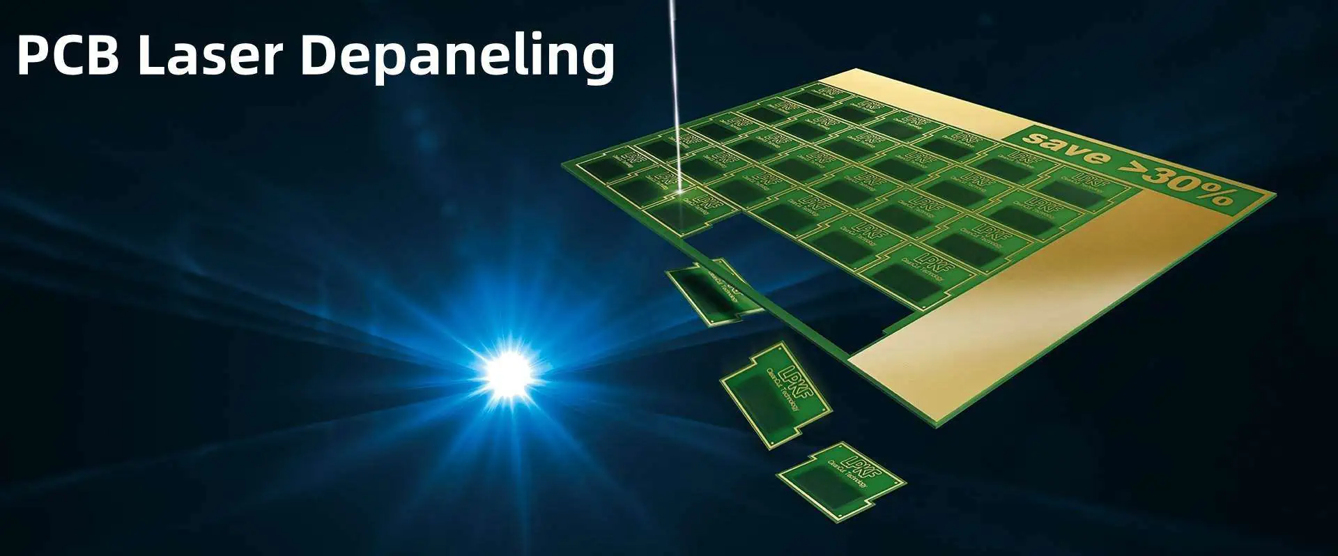
Laser depaneling is a cutting-edge technology that uses a focused laser beam to separate individual PCBs from a larger panel. This method offers numerous advantages over traditional mechanical depaneling techniques, especially when dealing with delicate or uniquely shaped PCBs like round ceramic boards.
The Science Behind Laser Depaneling
Laser depaneling works on the principle of material ablation. The laser beam, typically a CO2 or UV laser, is focused on the PCB material, vaporizing it along a predetermined path. This process creates a clean, precise cut without applying mechanical stress to the board.
Key Components of a Laser Depaneling System
Laser Source
Beam Delivery System
Motion Control System
Vision System
Exhaust and Filtration System
Advantages of Laser Depaneling for Round Ceramic PCBs
Precision: Laser cutting offers unparalleled accuracy, crucial for round shapes.
Stress-Free: No mechanical stress is applied to the delicate ceramic material.
Clean Cuts: Laser cutting produces smooth edges without debris.
Flexibility: Easily adaptable for various board shapes and sizes.
Programmability: Can be quickly reprogrammed for different designs.
Preparing for Laser Depaneling of Round Ceramic PCBs
Material Considerations
Ceramic PCBs have unique properties that make them ideal for certain applications but also require special handling during the depaneling process.
Development of more efficient and powerful laser sources
Advancements in automated handling and inspection systems
Conclusion
Laser depaneling of round ceramic PCBs represents a significant advancement in PCB manufacturing technology. By offering precision, flexibility, and stress-free separation, it enables the production of high-quality, complex PCB designs. As the electronics industry continues to demand more sophisticated and compact designs, the role of laser depaneling in PCB manufacturing is set to become increasingly important.
FAQ
Q1: Is laser depaneling suitable for all types of ceramic PCBs?
A1: While laser depaneling is suitable for most ceramic PCBs, the specific parameters may need adjustment based on the type of ceramic material, thickness, and board design. It’s particularly effective for round ceramic PCBs due to its precision in cutting curved paths.
Q2: How does the cost of laser depaneling compare to traditional methods?
A2: Initially, the setup cost for laser depaneling can be higher than traditional methods. However, it often proves more cost-effective in the long run, especially for high-volume production or when working with complex or delicate designs like round ceramic PCBs.
Q3: Are there any limitations to the thickness of ceramic PCBs that can be laser depaneled?
A3: While laser depaneling can handle a wide range of thicknesses, extremely thick ceramic PCBs may require multiple passes or a combination of techniques. The maximum thickness depends on the power of the laser and the specific properties of the ceramic material.
Q4: How does laser depaneling affect the electrical properties of ceramic PCBs?
A4: When done correctly, laser depaneling has minimal impact on the electrical properties of ceramic PCBs. The heat-affected zone is typically very small, and the process doesn’t introduce mechanical stress that could affect the board’s performance.
Q5: What maintenance is required for a laser depaneling system?
A5: Regular maintenance of a laser depaneling system typically includes cleaning of optics, checking and replacing filters, calibrating the laser and motion control systems, and inspecting for any wear or damage to components. The frequency of maintenance depends on usage but is generally less intensive than mechanical depaneling systems.
Nixie tubes represent a captivating piece of electronic history, offering a warm, vintage aesthetic that continues to fascinate electronics enthusiasts and hobbyists. This comprehensive guide will walk you through creating a Nixie tube clock using a unique freeform wire construction technique that eliminates the need for a traditional printed circuit board (PCB).
Understanding Nixie Tubes
What Are Nixie Tubes?
Nixie tubes are cold-cathode display devices invented in the 1950s, featuring a wire mesh anode and multiple cathodes shaped like numerals. When a specific cathode is energized, it glows with a distinctive orange-red color, creating a mesmerizing display of numbers.
Q1: Is a freeform wire construction as reliable as a PCB?
A: While different, a well-executed freeform construction can be equally reliable. Proper design, soldering, and mechanical support are key to long-term performance.
Q2: How dangerous is the high voltage in a Nixie tube clock?
A: High voltage components require careful handling. Always use proper insulation, avoid direct contact, and implement safety features like current limiting.
Q3: Can I use different types of Nixie tubes?
A: Yes, but ensure compatibility with your power supply and switching circuits. Verify pinout and voltage requirements for each tube type.
Q4: What’s the typical power consumption of a Nixie tube clock?
A: Approximately 2-5 watts, depending on tube type and display duration. Implementing power-saving modes can reduce overall consumption.
Q5: How long do Nixie tubes typically last?
A: Quality Nixie tubes can last 50,000-100,000 hours (5-11 years of continuous operation) with proper care and moderate usage.
Conclusion
Building a Nixie tube clock using freeform wire construction represents a challenging yet rewarding project that combines vintage electronics, precise engineering, and artistic expression. Each step requires careful consideration, technical skill, and creative problem-solving.
The journey of creating such a clock is as valuable as the final product—a testament to the enduring fascination of vintage electronic technologies and the maker’s spirit of innovation.
Introduction: Why 5V Regulator Protection is Critical
5V voltage regulators power the backbone of modern electronics, from Arduino projects to industrial control systems. However, without proper protection circuits, these essential components remain vulnerable to electrical stress that can cause catastrophic system failures. This comprehensive guide explores how to design robust protection circuits that safeguard your 5V regulators and ensure long-term reliability.
Understanding 5V Voltage Regulators
What is a 5V Regulator?
A 5V voltage regulator maintains a constant 5-volt output regardless of input voltage fluctuations or varying load conditions. These regulators are indispensable for powering:
Integration with IoT connectivity for remote monitoring and control.
Adaptive Protection
Algorithms that adjust protection parameters based on operating conditions.
Self-Healing Circuits
Systems that automatically recover from fault conditions.
Conclusion
Implementing comprehensive protection circuits for 5V regulators is essential for creating reliable electronic systems. By understanding the various failure modes and protection techniques, engineers can design robust circuits that prevent damage and ensure long-term operation.
The key to successful protection design lies in:
Identifying all potential failure modes
Selecting appropriate protection methods
Proper component sizing and placement
Thorough testing and validation
Balancing cost with protection requirements
With careful attention to these factors, your 5V regulator protection circuits will provide years of reliable service, protecting valuable equipment and preventing costly downtime.
Additional Resources
For more detailed information on specific protection components and design techniques, consult manufacturer application notes and industry standards such as IEC 61000 for electromagnetic compatibility and IEC 60950 for safety requirements.
Stripboard, also known as Veroboard, is a versatile and popular prototyping medium for electronic circuits. This comprehensive guide will walk you through the intricacies of creating circuits on stripboard, from understanding its basic structure to mastering advanced techniques for reliable and efficient circuit design.
Understanding Stripboard Basics
What is Stripboard?
Stripboard is a type of prototyping board consisting of a rigid substrate with parallel copper tracks running in a single direction. Unlike breadboards, stripboard provides a more permanent solution for circuit development and testing. Its simple yet effective design makes it a favorite among hobbyists, students, and professional electronics engineers.
Q1: How do I prevent short circuits on stripboard?
A: Carefully cut tracks between components, use insulating tape if needed, and always double-check your track cuts with a multimeter before powering the circuit.
Q2: Can I reuse a stripboard after desoldering components?
A: Yes, but be cautious. Excessive heating can damage copper tracks. Clean the board thoroughly and inspect for any track damage before reuse.
Q3: What’s the difference between stripboard and breadboard?
A: Stripboard provides a more permanent solution with soldered connections, while breadboards offer temporary, solderless prototyping with easy component replacement.
Q4: How precise do track cuts need to be?
A: Cuts should completely separate the copper track. Use a magnifying glass or continuity tester to verify complete separation.
Q5: Are there alternatives to manual track cutting?
A: Some advanced users employ chemical etching or laser cutting for precise track modifications, but manual cutting remains the most accessible method.
Conclusion
Mastering stripboard circuit construction requires practice, patience, and attention to detail. By understanding the fundamentals, investing in proper tools, and developing precise techniques, you can create robust and reliable electronic circuits.
Whether you’re a hobbyist, student, or professional, stripboard remains an invaluable tool in the electronics prototyping arsenal. Continual learning and experimentation will enhance your skills and expand your capabilities in electronic circuit design.


