12 Layer Rogers Laminate + FR4 Hybrid Dielectric Constant PCB

12 Layer Rogers+FR4 PCB circuit board

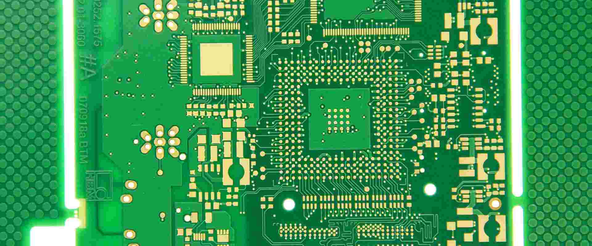
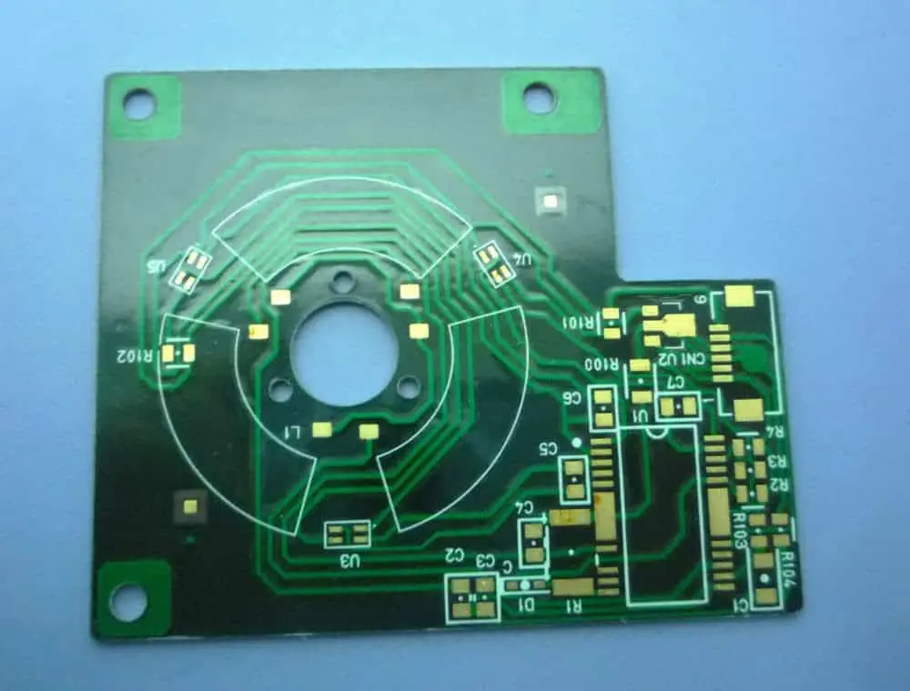
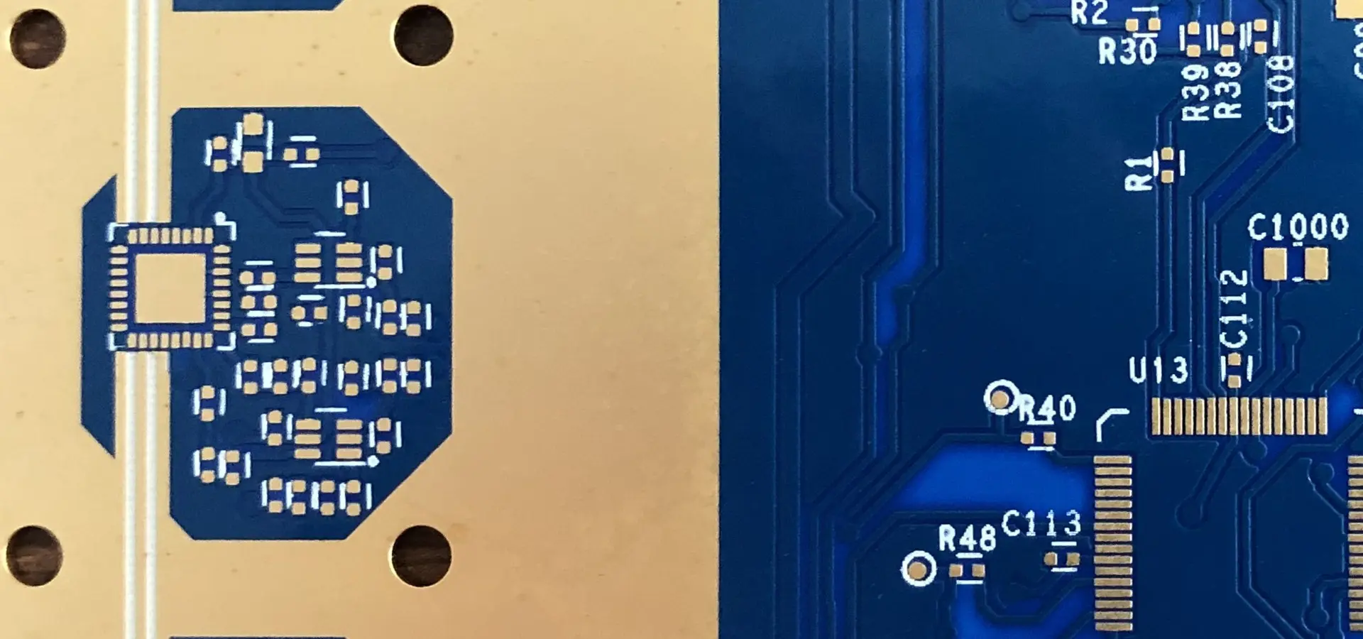
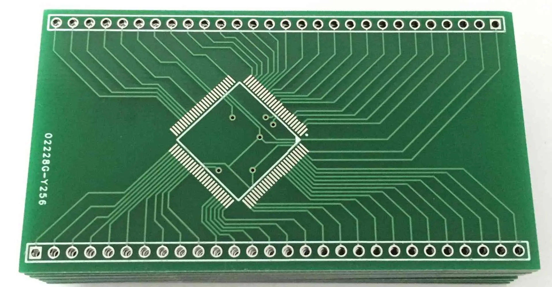
12 Layer Rogers + Fr4 PCB Multifunctional integrated copper plate

Layer : 12 layer pcb

Board thickness: 2.6mm

Copper thickness :1oz

Material: Rogers 4350B+FR4

Type: Metal Base Power Amplifier Board

Technical features: Integrated design

Local mixed pressure

PCB buried I/U copper

Control deep power amplifier

Uses: wireless communication base station

Need 12 layer pcb board stackup suggestion, pls contact us

Introduction

12 Layer Rogers+FR4 PCB

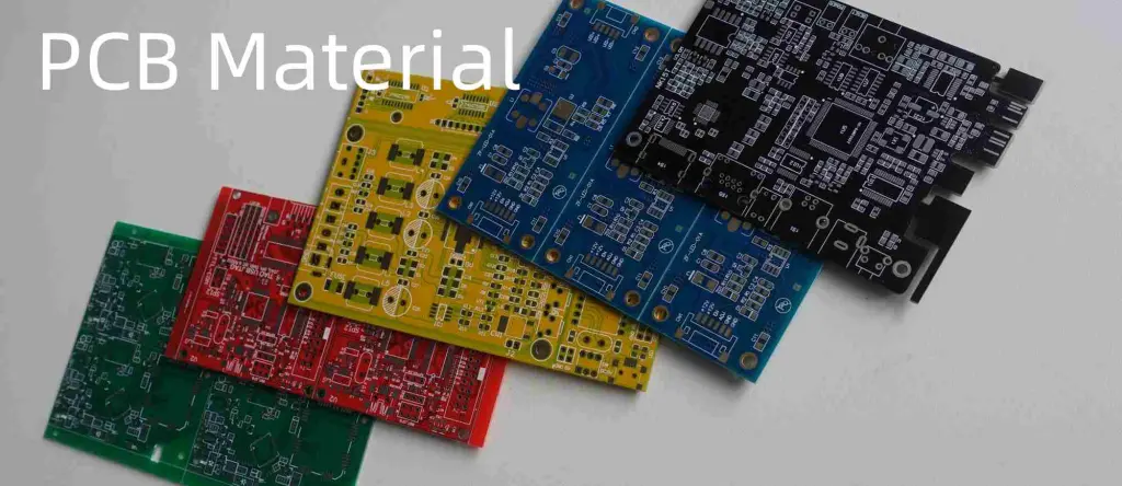
High performance and complex PCB designs often involve combining different laminate materials within a single circuit board stackup. A popular hybrid configuration uses standard FR-4 glass epoxy along with high frequency Rogers dielectric material in specific layers.

A 12 layer hybrid PCB with Rogers laminate and FR4 allows optimizing electrical performance and cost. This article provides an overview of hybrid 12 layer PCB stackups with Rogers and FR4 covering design, material selection, fabrication, applications and cost considerations.

Benefits of Rogers + FR4 Hybrid PCBs

Key advantages of using Rogers laminates selectively in a 12 layer FR4 PCB:

  • Signal Integrity: Provides tightly controlled impedance for high speed signals on Rogers layers
  • EMI Reduction: Rogers material has lower loss which improves signal quality and reduces EMI
  • Thermal Management: Higher thermal conductivity dissipates heat from high power components
  • Mechanical Stability: Rogers material has a lower Z-axis CTE providing enhanced structural stability
  • Selective RF Performance: High frequency analog circuits can be fabricated on Rogers layers
  • Cost Savings: Using Rogers only in essential layers with FR4 for rest reduces cost versus full Rogers stackup

Typical Stackup Configuration

A common 12 layer hybrid PCB stackup configuration is:

  • L1 to L4: FR-4 Dielectric
  • L5: Rogers 4350B Dielectric
  • L6 to L11: FR-4 Dielectric
  • L12: Rogers 4350B Dielectric

The higher performance Rogers 4350B material is used in the critical signal layers at the center of the stackup while standard FR-4 handles the rest of the routing.<img src=”https://drive.google.com/uc?export=view&id=1PUosbPyuqbxT-ShQLuKNy Tem5MCyA4GX” alt=”Rogers FR4 Hybrid Stackup” style=”width:300px;height:400px;”>

The exact layer distribution can be adjusted based on high speed and RF routing needs. Additional Rogers layers can be added near the surface for RF components requiring tight impedance control. Simulations help optimize the hybrid stackup configuration.

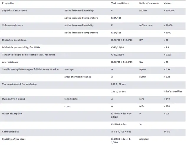
Rogers vs FR-4 Material Properties

Rogers 4350B offers better electrical and thermal performance than FR-4 but at a higher cost:

ParameterRogers 4350BFR-4
Dielectric Constant3.664.5
Loss Tangent0.00370.02
Impedance Tolerance±5%±10%
Glass Transition Temp>280°C130°C
Thermal Conductivity0.69 W/mK0.3 W/mK
Coefficient of Thermal Expansion40 ppm/°C14-18 ppm/°C
Moisture Absorption0.04%0.2%
Lead-free Process CompatibleYesYes
Relative CostHighLow

Rogers RF laminates allow reliable performance for circuits up to 77GHz. They are available in a range of dielectric constants from 2.2 to 10.2 to suit different applications. Popular alternatives are Rogers 4003C and 5880.

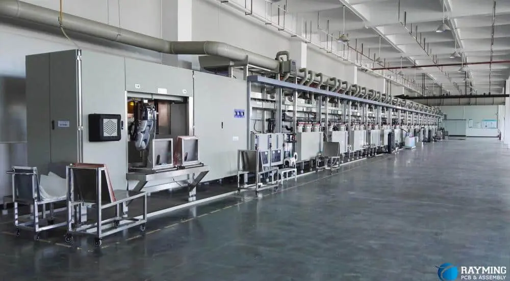
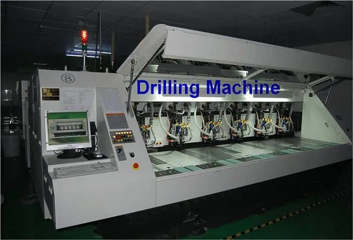
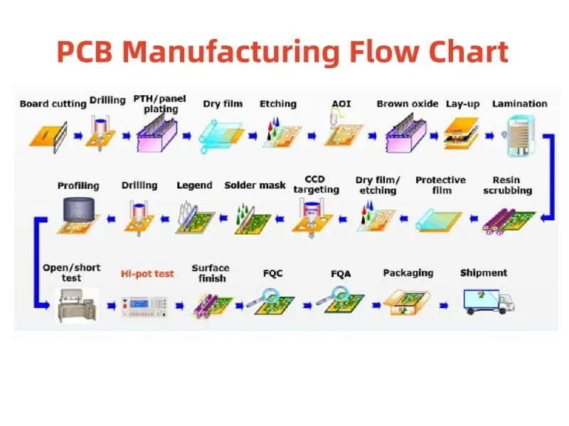
Hybrid PCB Fabrication Process

hybrid-pcb

Fabricating a hybrid multilayer PCB with dissimilar materials involves additional steps compared to standard FR-4 boards:

  • Materials from different suppliers are qualified for compatibility
  • Separate layup stacks for Rogers and FR-4 multilayers
  • Adhesion enhancers added at bonding interfaces
  • Modified lamination profile to account for property mismatches
  • Buried via formation requires staggered drilling and plating
  • Multiple alignment steps are required when combining layers
  • Bevel cutting bit used to avoid corner cracking
  • Expanded testing to validate electrical performance

Only manufacturers with experience in hybrid constructions should be chosen to mitigate the fabrication risks.

Design Guidelines

Some key design aspects for hybrid Rogers + FR4 PCBs:

  • Layer sequence: Order from middle outwards should progress from better to poorer performance
  • Interfaces: No components recommended to straddle Rogers-FR4 junctions
  • Transitions: Follow impedance transition rules when traces move between materials
  • Thermal density: Spread heat generating components across layers to avoid hotspots
  • Via transitions: Use annular rings when changing materials to avoid cracking
  • Testpoints: Include pads on both Rogers and FR4 layers for characterization
  • RoHS compliance: Both materials qualified for lead-free assembly

Simulations should account for the different dielectric constants between laminates while verifying impedance, timing, power integrity and EMI.

Applications

The capabilities of Rogers laminates make 12 layer hybrid boards suitable for:

  • High speed digital circuits
  • Serial bus interfaces like PCIe, USB 3.0
  • Networking products like switches, routers
  • Wireless communications infrastructure
  • Radar and antenna systems
  • Test and instrumentation

The integration of Rogers material in high layer count PCBs along with FR4 provides a robust solution for products requiring speed, precision and RF performance without the cost of using exotic dielectrics exclusively.

Cost Analysis

For a 300mm x 400mm board, a cost estimate comparison between full FR-4 and hybrid construction in 5000 piece prototype volumes:

Configuration12L Full FR412L Hybrid (Rogers in L5/L12)
Fabrication$130$160
Material$155$195
PTH Plating$210$250
Mask +Legend$130$145
Handling$55$60
Test$125$150
Total/board$805$960

The hybrid option with Rogers in 2 layers has around 20% higher cost. But the performance gain outweighs this cost premium in many high speed and RF applications.

Conclusion

Rogers PCB

Combining Rogers laminates and FR4 dielectric in a 12 layer PCB provides an optimized tradeoff between performance and cost. The integration of high frequency Rogers material in the core layers offers precision routing for signals demanding tight impedance control, low loss and crosstalk isolation within a reliable, industry-standard 12 layer FR4 multilayer board. With careful design planning andworking with fabricators experienced in hybrid multilayer constructions, the Rogers-FR4 hybrid approach enables modern PCBs to implement demanding applications in networking, communications, defense, instrumentation and other leading edge fields.

FAQs

What are some key benefits of using a hybrid PCB stackup?

Hybrid stackups allow optimizing electrical performance, thermal management, stability, density and cost by combining different materials selectively as per circuit needs.

What precautions are required when soldering hybrid PCBs?

Use a lower temperature solder alloy to avoid damaging the higher performance dielectric material. Ramp down temperatures slowly after reflow.

Can components be placed across Rogers-FR4 junctions?

This is not recommended as thermal stresses can induce cracks or delamination. Components should be fully placed over one material.

How are impedance matched traces implemented in hybrid PCBs?

Matching is achieved by using different trace widths on each dielectric layer according to the material dielectric constant. Transitions between widths can be tapering or abrupt.

What are thermal reliefs used for in hybrid boards?

Cutouts below pads and vias facilitate heat transfer into the higher thermal conductivity plane layers while limiting conduction into the outer layers.

Why Is China PCB Circuit Board So Low Cost?

Shengyi S1190 PCB

In today’s fast-paced electronics industry, the demand for Printed Circuit Boards (PCBs) continues to grow exponentially. As the backbone of electronic devices, PCBs play a crucial role in everything from smartphones to industrial machinery. Amidst this increasing demand, China has emerged as the undisputed leader in PCB manufacturing, offering high-quality products at surprisingly low costs. But what exactly makes China PCB circuit boards so affordable compared to those produced in other countries? This article delves into the factors behind China’s competitive edge in the PCB industry.

1. The Scale of China’s PCB Manufacturing Industry

1.1 China as the World’s PCB Manufacturing Hub

China’s dominance in the PCB manufacturing industry is undeniable. According to recent statistics, China accounts for over 50% of the global PCB production, with an annual output value exceeding $30 billion. This massive scale of production is largely concentrated in manufacturing hubs like Shenzhen, Guangzhou, and Dongguan in the Pearl River Delta region.

The clustering effect in these areas has created a robust ecosystem of suppliers, manufacturers, and supporting industries, all working in close proximity. This geographical concentration facilitates rapid communication, efficient logistics, and knowledge sharing, contributing significantly to cost reduction.

1.2 Economies of Scale

One of the primary reasons for China’s low-cost PCB production is the economies of scale achieved through mass production. When manufacturers produce PCBs in large quantities, the fixed costs associated with production (such as equipment, facilities, and setup) are spread across a greater number of units, effectively lowering the cost per unit.

Moreover, bulk purchasing of raw materials allows Chinese manufacturers to negotiate better prices with suppliers. This cost advantage is then passed down the supply chain, ultimately resulting in lower prices for customers.

2. Access to Raw Materials at Lower Costs

2.1 Local Availability of Core Materials

China’s vast manufacturing sector has fostered the growth of a comprehensive supply chain for PCB production. Core materials such as FR4 (the most common base material for PCBs), copper foils, and various laminates are readily available locally. This local availability eliminates the need for costly imports and reduces transportation expenses.

2.2 Vertical Integration of Supply Chains

Many Chinese PCB manufacturers have adopted a vertically integrated business model. This means they not only produce PCBs but also manufacture or source key components and materials within their own network. Such integration allows for better control over costs and quality, leading to more competitive pricing.

2.3 Lower Material Transportation Costs Within China

The strategic location of PCB factories near raw material suppliers significantly reduces transportation costs. The well-developed transportation infrastructure within China’s manufacturing hubs further enhances this advantage, allowing for quick and cost-effective movement of materials and finished products.

Read more about:

3. Advanced Manufacturing Technology and Automation

3.1 Investment in Modern PCB Manufacturing Equipment

Chinese PCB manufacturers have made substantial investments in state-of-the-art manufacturing equipment. Advanced technologies such as CNC drilling machines, laser cutting systems, and Automated Optical Inspection (AOI) systems have become standard in many Chinese factories. These technologies not only improve precision and quality but also increase production efficiency, thereby reducing costs.

3.2 High Throughput Production Lines

The implementation of high-throughput production lines in Chinese PCB factories has dramatically increased production speed and efficiency. Automated systems handle various aspects of PCB production, from material handling to testing, minimizing human error and reducing labor costs.

3.3 PCB Manufacturing Machine Costs in China

Interestingly, the cost of PCB manufacturing equipment in China is often lower than in other countries. This is partly due to local production of such machinery and partly due to government incentives for upgrading manufacturing technology. Lower equipment costs translate to lower overhead for manufacturers, contributing to the overall low cost of PCBs.

4. Government Policies and Industrial Support

4.1 Incentives and Subsidies for Electronics Manufacturing

The Chinese government has long recognized the importance of the electronics manufacturing sector and has implemented various policies to support its growth. These include tax incentives, subsidies for research and development, and financial support for companies investing in advanced technologies.

4.2 Infrastructure Development

Significant investments in infrastructure, including modern ports, efficient road networks, and reliable power supply, have greatly benefited the PCB industry. This well-developed infrastructure reduces logistical costs and improves overall operational efficiency.

4.3 Export-Friendly Trade Policies

China’s export-oriented policies have created a favorable environment for PCB manufacturers to sell their products globally. Various trade agreements and export incentives have made it easier and more cost-effective for Chinese companies to reach international markets.

5. Lower Labor Costs Compared to Other Countries

5.1 Skilled but Cost-Effective Workforce

While labor costs in China have been rising in recent years, they remain significantly lower than in many developed countries. The PCB industry in China benefits from a large pool of skilled workers who are proficient in various aspects of PCB manufacturing, yet command wages that are competitive on a global scale.

5.2 Specialized Training Programs

Many regions in China have implemented specialized training programs focused on PCB assembly and testing. These programs ensure a steady supply of skilled workers, reducing training costs for manufacturers and maintaining a high level of expertise in the workforce.

5.3 Labor Cost Comparison

When compared to countries like the USA, Japan, or those in Europe, China’s labor costs in the PCB industry can be 50-70% lower. This significant difference in labor expenses plays a crucial role in keeping overall production costs down.

6. Highly Competitive Domestic Market

6.1 Intense Competition Among PCB Manufacturers

The PCB industry in China is characterized by intense competition among numerous manufacturers. This competitive environment leads to continuous price wars, forcing companies to optimize their processes and reduce costs to remain viable. While challenging for the manufacturers, this competition ultimately benefits customers through lower prices.

6.2 Impact of Competition on Innovation and Efficiency

The fierce competition in China’s PCB market has spurred innovation and efficiency improvements. Manufacturers constantly seek ways to streamline their processes, reduce turnaround times, and offer value-added services like rapid prototyping. This drive for efficiency further contributes to cost reduction and improved service quality.

7. Specialization in Different PCB Types

7.1 Standard PCB vs. Custom PCB Manufacturing

Chinese manufacturers have become highly efficient in producing standard PCBs, such as 2-layer and 4-layer boards. The streamlined processes for these common configurations allow for faster production and lower costs. However, many Chinese manufacturers also excel in custom PCB production, offering competitive prices for specialized designs.

7.2 Diverse PCB Offerings at Low Prices

The specialization extends to various PCB types, including flexible PCBs, LED PCBs, and amplifier PCBs. By focusing on specific niches, manufacturers can optimize their processes and offer these specialized products at surprisingly low prices. This specialization allows for economies of scale even in more complex PCB types.

8. Efficient Logistics and Global Shipping

8.1 Strategic Location of PCB Factories

Many PCB factories in China are strategically located near major ports and transportation hubs. This proximity reduces domestic transportation costs and facilitates quick and easy shipping to international markets.

8.2 Partnered Logistics Companies

Chinese PCB manufacturers often have partnerships with logistics companies that offer competitive shipping rates. These partnerships, combined with the high volume of shipments, allow for significant cost savings in international shipping.

8.3 Role of Online PCB Services

Companies like PCBWay and JLCPCB have revolutionized the global distribution of PCBs from China. These online platforms offer user-friendly interfaces for ordering custom PCBs, provide instant quotes, and manage the complexities of international shipping, making it easier than ever for global customers to access low-cost Chinese PCBs.

9. Common Misconceptions About Cheap China PCBs

9.1 Is Lower Price Equal to Lower Quality?

A common misconception is that low-cost PCBs from China are of inferior quality. While it’s true that some low-end manufacturers may cut corners, many Chinese PCB manufacturers produce high-quality boards that meet or exceed international standards. The key is to choose reputable suppliers with proper certifications and quality control processes.

9.2 Risks to Watch Out For

While the Chinese PCB market offers excellent opportunities for cost savings, buyers should be aware of potential risks. These include the possibility of counterfeit components in some supply chains and inconsistent quality from less reputable manufacturers. Due diligence in supplier selection is crucial to mitigate these risks.

10. How to Leverage China’s PCB Market Effectively

10.1 Tips for Choosing a Good Manufacturer

When selecting a Chinese PCB manufacturer, consider the following:

  • Look for relevant certifications (ISO 9001, UL, RoHS, etc.)
  • Check customer reviews and testimonials
  • Verify their testing standards and quality control processes
  • Request samples before placing large orders
  • Assess their communication responsiveness and English proficiency

10.2 Balancing Cost, Quality, and Lead Time

While low cost is attractive, it’s important to balance it with quality requirements and lead times. Sometimes, paying a slightly higher price can result in better quality, more reliable delivery, or enhanced customer service, which can save money and headaches in the long run.

Conclusion

The low cost of China PCB circuit boards is the result of a complex interplay of factors, including economies of scale, advanced manufacturing technologies, lower labor and material costs, government support, and intense market competition. These elements combine to create an environment where high-quality PCBs can be produced at remarkably low prices.

For startups and established companies alike, China remains a smart choice for PCB sourcing. The country’s PCB industry offers a compelling combination of cost-effectiveness, quality, and production capacity that is hard to match elsewhere in the world.

However, it’s crucial to approach PCB sourcing from China with due diligence. By carefully selecting manufacturers, understanding the market dynamics, and balancing cost considerations with quality requirements, businesses can fully leverage the advantages of China’s PCB industry while mitigating potential risks.

As the global electronics industry continues to evolve, China’s position as a leader in low-cost, high-quality PCB manufacturing seems secure for the foreseeable future. Whether you’re working on a small prototype or planning large-scale production, China’s PCB industry offers solutions that can significantly impact your project’s success and bottom line.

Why Is Cem-1 PCB Material still Popular in the Circuit Board Market ?

cem 1 pcb circuit board

Cem-1 PCB material ?   

Is so strange for the most of people ,  is one of Base Material for printed circuit boards. Is low grade in the PCB material industry , Only for Single side PCB, But it is used very widely .

Some People will say  Now Technology  develop so fast , Every Electronic device become smaller and thinner . Why so low grade material can be use widely .

Is true , Technology is becoming higher and higher , but mean time , Components is also high assemblied more function , This will let more designer use single side PCB ( Cem-1 Material ) to control their Cost .

Single Side PCB ( One Layer PCB )  will reduce the design cost very much , that’s the most important reason .

Cem-1 Material

CEM 1 PCB
CEM 1 PCB

he materials suitable under the CEM-1 specification in classification of NEMA – the most widespread materials for production of 1-layers printed circuit boards.

Standard CEM-1 material is composite material on a cellulose basis with one layer of glass fibre laminate (FR-4) on a surface. Usually CEM-1 has milky-white color.

The feature of this material is the impossibility of realization the metallization through holes, thus, this material can be used only for production of 1-layer printed-circuit boards.

Standard CEM-1 satisfies to combustibility class UL 94-V0, as FR-4 material. Mechanical characteristics of CEM-1 are little bit worse, than at FR-4: CEM-1 is more fragile. The dielectric constant and a tangent of angle of dielectric losses of both materials are differ insignificantly.

Thus, CEM-1 is a cheaper alternative for FR-4 material for production of 1-laye prototype printed-circuit boards.

CEM-1 PCB Material Technical parameters

In Cem PCB Material Family  ,Have other better one CEM-3 ,    Let’s see the difference CEM-1 and CEM -3

FULL PCB MANUFACTURING Quote

CEM-1 Composite material composed of woven glass fabric surfaces and paper core combined with epoxy resin. Primarily used in the printed circuit board industry. Easy punching and excellent electrical properties and higher flexural strength than paper based grades. CEM-1 provides excellent mechanical and electrical properties, and punches well up to .093″.

CEM-3 is very similar to FR4. Instead of woven glass fabric a ‘flies’ type is used. CEM-3 has a milky white color and is very smooth. It is a complete replacement for FR4 and has a very large market share in Asia. It is a kind of flame retardant epoxy copper-clad plate glass material, is generally used in electronics with double sided and multilayer pcb boards. And CEM – 3 is a new printed circuit substrate material developed based on FR – 4. In recent years, CEM-3 is used to replace FR-4 in Japan, even more than the FR – 4 dosage.

In Led lighting Market ,Most of Led PCB Manufacturer  use Cem1 as base Material . it can give the best balance between The heat dissipating performance and PCB cost .

In Next article we will introduce more low grade PCB material  for our electronic designer , give a low Cost PCB solution to you .

Fr1 . FR2 , FR3, 22F, CEM 1 ,Cem 3 . FR4, FR5,   What’s difference between them ? How to Choose the suitable material for your design?  how to control your PCB cost , Let ‘s wait the next article coming .

16 Q&A – How to Choose a manufacturer for PCB hobbyist?

printed circuit board manufacturers

Introduction

Printed circuit boards (PCBs) form the core of an electronics hobbyist’s projects. For professional looking, functional boards that bring your design ideas to life, choosing the right PCB manufacturer is key. This article covers the key factors to consider when selecting a PCB fabrication partner as an electronics hobbyist through 16 commonly asked questions:

Q1. What volume of PCBs do I need as a hobbyist?

For hobbyists and makers, the typical quantity of boards required for a project is usually quite low – ranging from just 1-2 prototype boards for testing up to about 50-100 boards for small scale building. This is considered low volume in PCB fabrication. So look for manufacturers that can support prototyping and small batch orders.

Q2. What size of PCBs will I need?

Typical PCB sizes in hobbyist projects range from 10mm x 10mm boards for tiny circuits to about 200mm x 100mm for more complex projects. Maximum sizes can go up to 300mm x 300mm but usually not larger. Select a vendor that can fabricate boards in this range of compact sizes.

Q3. What PCB technology choices do I have?

Hobbyist boards are typically 2 layer or 4 layer designs using standard FR-4 material. Some projects may need 6 layers or flex PCBs. Ensure your vendor can handle layer counts from 1 to 6, different dielectric materials, trace/space down to 5 mil, plated slots/holes, gold plating, carbon printing etc.

Q4. What budget should I allocate for PCB fabrication?

LPI PCB
LPI PCB

For prototype 2 layer boards of 50mmx50mm size, expect costs of around $5 to $10 per piece for 10-piece quantity from China. For larger 4 layer boards up to 200x200mm in 10-pc quantity, costs are approximately $50-100 per board. Budget 1.5 to 2 times more for very quick turnaround.

Q5. What are the PCB fabrication process capabilities needed?

Look for suppliers offering: solder mask, silkscreen legend, controlled impedance, HAL, minimum hole sizes of 0.2mm, copper thickness up to 2 oz., Underwriters Lab (UL) approval, RoHS compliance and lead-free processing. Not all of these may be needed but having these capabilities ensures your supplier can meet future needs as projects increase in complexity.

Q6. How do I check the reliability and quality of the PCB manufacturer?

Ask about their quality certifications like ISO 9001. Review online testimonials and feedback on forums. Evaluation samples from potential vendors. Ask detailed questions on their quality assurance practices. A reliable manufacturer will be transparent and even allow site visits.

Q7. What special services do I need as a hobbyist?

Hobbyists need:

  • Low NRE (non-recurring engineering) charges or none for complex designs
  • No minimum order quantity – ability to order single pieces
  • Quickturn fabrication in 3-5 days to test designs faster
  • Basic assembly services to get ready boards
  • Virtual communication for design reviews

Q8. What support for design is important?

Design support services that help hobbyists include:

  • Online quotes based on your uploaded Gerber files
  • Free DFM (design for manufacturing) analysis to check your design against fab norms
  • Quick online communication for design reviews
  • Prototype PCB fabrication in 24-48 hours
  • Supplying required design libraries and templates

Q9. How do I assess technical capabilities of a PCB manufacturer?

Review their technology roadmap and offerings vs industry standards to assess technical competence – things like line/space capabilities, microvia sizes, impedance control tolerances, HDI stacking abilities etc. The right partner for an advanced hobbyist should have strong technical expertise.

Q10. What certifications should I look for in a PCB supplier?

Relevant quality and sustainability certifications include:

  • ISO 9001 or AS9100 – Quality management
  • ISO 14001 – Environmental
  • IATF 16949 – Automotive quality
  • UL – Product safety testing
  • RoHS – Hazardous substances process control
  • IPC standards – PCB manufacturing

Q11. How important are environmental factors in choosing a PCB supplier?

As a hobbyist, ensuring your PCB manufacturer follows environmental rules on wastewater treatment, emissions norms, chemical handling etc. promotes sustainability. They should be REACH and RoHS compliant. If they have ISO 14001 certification, even better.

Q12. Does manufacturer location matter for a hobbyist?

Location has a major impact on cost, lead time and communication access for on-demand prototyping needs. For fastest turnaround and cost savings, use manufacturers based in China. But also consider your intellectual property security when sharing design information.

Q13. How do I evaluate potential PCB manufacturers before selecting one?

Ways to evaluate suppliers:

  • Get free design review and quotation
  • Review online reputation and testimonials
  • Assess responsiveness of sales and engineering team
  • Ask for samples of similar PCBs built recently
  • Validate quality certifications and technical expertise

Q14. What questions should I ask PCB manufacturer before ordering?

PCB drilling machine

Important questions hobbyists should clarify:

  • What are your capabilities in PCB fabrication and assembly?
  • What engineering support do you provide during design?
  • What design standards do you follow?
  • What quality control checks are performed during manufacturing?
  • How do you ensure protection of my IP/design data?
  • What certifications have you obtained?
  • Do you have liability insurance to cover defects?

Q15. What are signs of a good PCB manufacturer for prototype projects?

Characteristics of a good prototyping partner:

  • No minimum order quantity
  • Quickturn fabrication in 3-5 days
  • Low NRE (non-recurring engineering) charges
  • Willingness to fabricate low volumes
  • Capability to scale to medium volumes
  • Good design and engineering support
  • Quality and reliability focused

Q16. What mistakes should I avoid when choosing a PCB supplier as a hobbyist?

Common mistakes to avoid:

  • Selecting purely based on lowest price quotes -Going with unknown, new companies without reputation
  • Assuming overseas companies have lower quality
  • Not checking their qualifications and certifications
  • Not reviewing prototypes before larger builds
  • Not having a robust manufacturing agreement

Conclusion

Choosing the right PCB manufacturing partner is key to ensuring success as an electronics hobbyist. Evaluating suppliers based on capabilities, services, quality, responsiveness, and costs helps identify the best prototyping partner for your unique needs. With the right selection, hobbyists can fully realize their PCB designs and product ideas.

Key Takeaways

  • Focus on manufacturers equipped for low volume prototyping
  • Leverage design support services like DFM analysis
  • Prioritize quality, reliability and technical capabilities
  • Evaluate based on certifications, customer reviews and pre-production sampling
  • Analyze total costs not just unit prices
  • Align supplier location and capabilities with target lead times
  • Establish effective communication channels and IP protection

Recommendations

Reliable PCB suppliers with strong support for hobbyist prototyping include:

  • Rayming Technology- China based, excellent engineering support
  • Seeed Studio – China, community marketplace and Fusion PCB service
  • JLCPCB – China, very fast delivery at low cost
  • OSH Park – US based, small batches with quickturn
  • Eurocircuits – Europe, proven quality and 25+ years experience

With the right partner, hobbyists can take their electronics projects from concept to reality smoothly.

Metal PCB Materials Differences: Aluminum Vs. Copper Core Vs. Iron Based

mcpcb manufacturer

Introduction

Metal core printed circuit boards (MCPCB) refer to boards which incorporate a metal plate or substrate as the central layer instead of the typical FR4 dielectric. Metals like aluminum, copper or iron alloys can be used as the core material in MCPCBs.

The high thermal conductivity of the metal core enables heat dissipation from mounted electronic components. This makes MCPCBs well suited for thermal management in applications with high power devices.

This article provides a detailed comparison between the different metal core materials used in PCBs covering properties, performance, applications, pros/cons and costs.

Aluminum Core MCPCB

aluminum substrate pcb

Aluminum is the most common metal base material used in metal core PCBs due to its combination of good thermal performance, ease of fabrication and lower cost:

Typical properties:

  • Thermal conductivity: 130 W/mK
  • Coefficient of thermal expansion (CTE): 23 ppm/°C
  • Density: 2.7 g/cm3
  • Specific heat capacity: 0.9 J/g°C
  • Availability of alloys like 6061, 5052, 2024 etc.

Key attributes:

  • Excellent heat dissipation performance
  • Cost effective material and processing
  • Lightweight
  • Well-established PCB technology
  • Can be easily machined or punched
  • Recyclable

Typical thickness range:

  • 0.5mm to 6mm plates
  • 1mm to 2mm is common

Applications:

  • LED lighting
  • Power converters
  • Motor drives
  • Power supplies
  • Solar inverters
  • Automotive electronics

Aluminum MCPCBs offer the best balance of thermal performance, manufacturability and cost for most mid-to-high power electronic circuits.

Copper Core MCPCB

Copper provides significantly higher thermal conductivity than aluminum. This makes it useful for very demanding thermal applications:

Properties:

  • Thermal conductivity: 400 W/mK
  • CTE: 17 ppm/°C
  • Density: 8.9 g/cm3
  • Specific heat capacity: 0.39 J/g°C

Benefits:

  • Extremely high thermal conductivity
  • Well-established PCB technology
  • Widely available
  • Can be fabricated using standard FR4 processes
  • Solderable and recyclable

Typical thickness range:

  • 0.25mm to 4mm
  • 0.5mm to 2mm common

Applications:

  • High power LED lighting
  • RF power amplifiers
  • Power modules
  • Solar microinverters
  • High density computer systems

The excellent thermal performance of copper MCPCB justifies its higher cost in applications where thermal dissipation is critical for reliability.

Iron Alloy Core MCPCB

Iron alloys containing nickel, cobalt, aluminum etc. offer a lower cost alternative to copper for improved thermal conductivity over aluminum:

Properties vary by composition:

  • Thermal conductivity: Up to 65 W/mK
  • CTE: 10-15 ppm/°C
  • Density: 7-8 g/cm3
  • Specific heat capacity: 0.44-0.46 J/g°C

Benefits:

  • Higher thermal conductivity than aluminum
  • Lower cost than copper
  • Compatible with FR4 fabrication
  • High strength for thin cores

Typical thickness range:

  • 0.1mm to 3mm plates
  • 0.2mm to 0.5mm common

Applications:

  • LED lighting
  • Industrial electronics
  • Telecom systems
  • Automotive

Iron alloys like iron-nickel-cobalt provide a good compromise between performance and cost for an intermediate thermal conductivity core material.

Comparing Metal Core PCB Materials

Key properties of the main metal core PCB base materials:

ParameterAluminumCopperIron Alloy
Thermal conductivity130 W/mK400 W/mKUp to 65 W/mK
CTE23 ppm/°C17 ppm/°C10-15 ppm/°C
Density2.7 g/cm38.9 g/cm37-8 g/cm3
Specific heat0.9 J/g°C0.39 J/g°C0.44-0.46 J/g°C
CostLowHighMedium
Common thickness1-3mm0.5-2mm0.1-0.5mm

General material selection guidelines:

  • Aluminum – Cost-driven applications where thermal conductivity >130 W/mK is sufficient
  • Copper – Where maximum heat dissipation is critical
  • Iron alloy – Applications constrained by weight or cost but need higher thermal performance than aluminum

Metal Core MCPCB Fabrication

Fabricating metal core PCBs requires specialized processes compared to standard FR4 PCB construction:

Base Metal Preparation

The metal is cut into specified panel sizes and thicknesses. Holes are punched for mounting components if needed. The surfaces are chemically cleaned.

Dielectric Layer Lamination

Thin dielectric films like polyimide or FR4 prepregs are laminated onto the metal core under pressure and temperature. Bonding agents help adhesion.

Circuit Formation

Similar to rigid PCB fabrication, the circuit layers are formed on the dielectric layers using processes like photolithography, plating and etching.

Component Assembly

Components can be conventionally soldered. For higher heat tolerance, sintering of silver paste or transient liquid phase bonding is used.

Enclosure Integration

The metal core MCPCB can sometimes directly serve as a housing or enclosure surface for mechanical stiffness, shielding and heat spreading.<img src=”https://drive.google.com/uc?export=view&id=1pNpZjav6MG438K0wGShZbZ8eqy3llH-S” alt=”metal core PCB fabrication” style=”width:500px;height:300px;”>

The specialized materials, processes and integration considerations involved in metal core PCB manufacturing demand working with an expert supplier.

Aluminum MCPCB Pros and Cons

Benefits of aluminum metal core PCBs:

  • Excellent thermal conductivity for heat dissipation
  • Cost-effective material and fabrication
  • Lightweight construction
  • Mature, established manufacturing processes
  • Readily machinable or punchable
  • Solderable and recyclable

Limitations of aluminum MCPCBs:

  • Lower thermal conductivity than copper or alloy cores
  • Higher CTE than copper causes greater component warping stresses
  • Susceptible to corrosion in harsh environments
  • Lower stiffness than steel or copper cores when very thin
  • Not suitable for high frequency or precision circuits

Aluminum strikes the best balance between cost, performance and manufacturability for most commercial thermal management PCB applications.

Copper MCPCB Pros and Cons

Advantages of copper metal core PCBs:

  • Extremely high thermal conductivity
  • Well-established PCB manufacturing processes
  • Widely available material supply
  • Can often reuse fabrication lines for rigid FR4 PCBs
  • High temperature soldering capability
  • Recyclable material

Drawbacks of using copper as metal core:

  • Substantially higher cost than aluminum
  • Heavy weight increases product weight
  • Thermal expansion issues when paired with non-CTE matched components
  • Lower brilliance compared to aluminum with LEDs
  • Lower dielectric strength than aluminum at thinner gauges
  • Requires nickel plating for solderability

The unmatched thermal performance of copper justifies its usage where removing heat is absolutely critical for application success.

Iron Alloy MCPCB Pros and Cons

Benefits of iron alloy metal core PCBs:

  • Higher thermal conductivity than aluminum
  • Lower density than copper provides weight savings
  • Cost is between aluminum and copper
  • High yield and tensile strengths when thin
  • Manufacturing processes similar to FR4 PCBs

Challenges with iron alloys for metal core PCBs:

  • Thermal conductivity still lower than copper
  • Material options not as diverse as aluminum or copper alloys
  • More difficult to fully recycle
  • Higher loss at high frequencies than aluminum or copper
  • Lower stiffness than aluminum or copper at identical thickness

Iron alloys offer a viable intermediate option where cost or weight are key constraints but thermal performance must exceed aluminum.

Cost Comparison

Metal core PCB cost considerations:

  • Metal core PCBs have higher fabrication cost than FR4 PCBs due to specialized materials, processes and lower panel utilization.
  • However, the ability to remove heat from high power components results in overall system cost savings.
  • Aluminum core is the most economical metal base material. Iron alloy adds moderate cost increment over aluminum. Copper core can double the cost over aluminum.
  • But metal core PCB cost is typically a small fraction of overall system cost for an electronic product. The thermal and reliability benefits justify the premium.
  • Cost reduces in high production volumes due to improved material utilization and manufacturing efficiency.

Applications of Metal Core PCBs

Some common application areas where metal core PCBs provide benefits include:

LED Lighting

The high power LEDs used require metal core PCBs for heat extraction. Aluminum is widely used but copper or iron allows driving LEDs at higher currents for greater luminosity.

Power Converters

Switching converters and inverters for power electronics require metal core PCBs to manage substantial heat dissipation from components like inductors and FETs.

Motor Drives

Motor drives work under challenging operating temperatures. Metal core PCBs allow efficient thermal management in the tightly packed drives.

Servers

Within data centers, high compute density server blades need effective cooling to maintain reliability.

RF Power Amplifiers

High frequency RF amplifiers using GaAs or GaN ICs benefit from the electrical and thermal conductivity of copper metal core PCBs.

Aerospace & Defense

Rugged aluminum or copper core PCBs meet demanding thermal and mechanical performance requirements in aerospace and military applications.

Conclusion

Metal core PCB technology enables integration of electronic components and systems with higher power densities by effectively managing dissipated heat. Aluminum, copper and iron alloys provide a range of core material options to suit different design constraints and applications. Aluminum MCPCBs offer the best value for most cost-driven commercial applications demanding higher thermal conductivity than standard FR4 PCBs. Where maximum heat transfer is critical for product functioning, the highest performing copper MCPCBs are the optimal choice despite increased cost. Iron alloys provide a middle ground alternative. With each material having unique benefits and tradeoffs, designers must make informed selections to match the metal PCB technology used to the specific thermal, weight, frequency, mechanical and cost requirements of the application.

FAQs

What are some key considerations when selecting metal core PCB thickness?

Some guidelines for choosing thickness:

  • Thicker cores allow mounting larger, higher power components
  • Thinner cores weigh less but have reduced stiffness
  • Thicker cores increase trace lengths if routing on outer layers
  • Optimal thickness balances weight, cost and layout space

What fabrication challenges are common with metal core PCBs?

Some potential issues include:

  • Delamination or cracking due to CTE mismatches
  • Voids or lack of adhesion with dielectric bonding
  • Drilling precision on thicker metal cores
  • Higher scrap rates and lower panel utilization
  • Warping when cooling after lamination

How are components assembled on MCPCBs?

Assembly options:

  • Conventional SMT soldering for moderate temperature parts
  • Sintered silver joints for high power devices
  • Transient liquid phase soldering where high heat capacity is required
  • Press fit pins, clips or thermal adhesives for selective mounting

What alternatives exist to using metal core PCBs for thermal management?

Some options are:

  • Thick copper planes within conventional PCBs
  • Thermal cladding, gap pads or vias for heat extraction
  • Heat sinks, heat pipes or cold plates attached to PCBs
  • Liquid cooled plates with internal fluid circulation
  • Insulated metal substrate PCBs

Are electrically insulating coatings required on metal cores?

Yes, the metal core must be coated with insulating dielectric films on both sides to avoid electrical shorts. This adds material cost but allows routing signals like conventional PCBs.

Printed Circuit Board Manufacturing and Aluminum Based PCB

metal core pcb vias

Printed Circuit Board Manufacturing and Aluminum-Based PCBs

A tremendous changing everywhere can be seen as the concept of everything and work has been changed completely. Nowadays, electronic appliances are not an exception to this changing. Today, the electronic manufacturing heavily depends on the quality of printed circuit board and its manufacturing. Because of the broad use of these innovative boards in electronic appliances like television, computer cell phones and even in tiny cables has persuaded renowned manufacturers to get involved in PCB manufacturing.

Aluminum PCB Board
Aluminum PCB Board

Since their inception, a tremendous changing can also be seen in the printed circuit manufacturing as previously they were manufactured by using polyester as well as polyimide materials. But, today aluminum based PCBs have captured the market. Apart from this they also have the first choice, when it comes to electronic manufacturing. There are a number of benefits associated with aluminum-based PCBs as aluminum is safe and durable. Apart from this, it is lightweight that can be used for any purpose.

YouTube video

Moreover, it can also afford the heat and electricity conductivity in those electronic applications that are more prone to get quick heat. Moreover, in PCB manufacturing, using a base that should have excellent heat as well as electrical conductivity is vital. And aluminum is the metal that is a perfect base for PCB manufacturing for the dissipation of heat devoid of extra heat sinks. In addition the aforesaid benefits of aluminum, there are also a number of other benefits associated with it. It is a common fact that aluminum is the most commonly used metal used in power transmission lines globally and it eliminates the effect of thermal stress on all the modules.

In this way, aluminum-based PCBs are very helpful in increasing the life of electronic manufacturing and appliances. Reducing the temperature of component operating, improving reliability and also improving thermal conductions are some of the added advantages of aluminum-based PCB manufacturing. Because of having a number of benefits of aluminum-based PCB, they are also called metal core printed circuit boards. A doctor to thermal conduction that leads to versatility in component tracking layout, aluminum-based PCB manufacturing also make them more useful.

The PCB Manufacture, Manufacturing, and the Aluminum PCB

PCB stands for the printed circuit board. The manufacturing of this printed board specializes in the prototype to medium production volumes. There is a wide range of products that are the latest in the industry of the PCB. These products are accompanied by the latest model of the equipment’s to produce precise boards and meet the requirements. No matter what one’s special needs and applications are the printed circuit board will work to meet them. The circuit boards that come from the printed board are good and they exceed the expectations of the user. A printed circuit board is a mechanically devised path, track or pathway leading to the electronic receipt and connection of electronic devices.

PCB: How to Choose the Right One

It is very important to choose the right manufacturer while selecting an electric board for a device. One-sided; two-sided as well as multi-layered circuit boards are available and are utilized in different devices these days. The multilayered boards are usually used in small devices and they are settled one upon another. Some of these boards are also available with aluminum plating or hot air leveling.

A number of companies have a knowhow of designing electronic boards of different sizes and they also provide with several materials used for the production purpose. These materials are tested and verified time and again so that the customers can get smooth working devices. It takes a lot of time and effort to learn about the designing of a printed circuit board. Thus, instead of going through such a complex process, it is always advisable to order them from a trustworthy and experienced company or resource.

Aluminum PCB Applications

Aluminum is one of the world’s widely used metal. Its use is not limited to industrial purposes alone, and can also be seen in homes, offices, and highways. This metal is also used in building vehicles due to its remarkable ability to withstand corrosion. The metal is also renowned for its low-density characteristic.

Since aluminum is malleable, using it for various purposes is not difficult. It is perfect for vehicles and can be used in machinery since it does not ignite easily unlike other metals. Apart from this, it is also a hundred percent recyclable, which makes it a favorite among recycling centers and junkyards. This metal also maintains its physical properties even after it is recycled.

PCB manufacturing involves many materials and many procedures that come with it. The PCB manufacturer makes sure that when they manufacture this board they are accompanied by the safety measures that they need to be followed when you are handling this printed board. The dimensions of the board, including the entire diameter, copper wire thickness, and material length, are closely monitored in the manufacture of these products. Before the printed circuit, there was the point to point constructions were used. Originally the electronic components had wire leads and the printed circuit board had holes drilled for each wire of each component. There are many types of the aluminum-based PCB that exist. All these types are useful to you as an individual. Their makes are unique and hence they are long-lasting. There are many types of the aluminum base PCB that are there in the market today depending on what you want. There are the aluminum printed boards for led, the aluminum PCB for high power led, led street light, high thermal led and the aluminum board for the garden lamp.

Assembly of RO4350B PCBs for Military High Frequency Products

military rogers pcb board
Military PCB Board
Military PCB Board

Supporting the military is something RayMing is very proud of, and we were contracted to assemble a PCB for use in a military communications application. The RF prototype PCB assembly used Rogers 4350B material, and the board required surface mount technology for the double-sided assembly that featured 250 placements. Board specs included 3 layers, standard vias, and 1 panelization. Final measurements came to 8 x 5.75 in. We performed final testing using automated optical inspections and x-ray inspection before delivering product to the customer.

Introduction

Rogers RO4350B laminates are widely used for manufacturing high frequency PCBs for defense and aerospace applications like radars, electronic warfare systems, satellite communications, etc. This high performance PCB material enables circuits to operate reliably at microwave and mm-wave frequencies beyond 10 GHz.

However, assembling PCBs using RO4350B substrates requires special considerations during fabrication, component selection and assembly processes owing to its unique properties. This article provides guidelines on how to assemble RO4350B PCBs for mission-critical military applications.

RO4350B PCB Material Properties

ro4350 pcb

RO4350B is a glass reinforced fluoropolymer composite circuit board material designed for exacting microwave and mm-wave circuit needs. Here are some of its key properties:

  • Dielectric constant (Dk) of 3.48 at 10 GHz
  • Low loss tangent of 0.0037 at 10 GHz
  • Woven glass reinforced hydrocarbon/ceramic filled PTFE composite
  • Good thermal conductivity of 0.69 W/m/K
  • Low Z-axis CTE of 41 ppm/°C
  • Glass transition temperature of 280°C

RO4350B’s electrical and mechanical attributes make it suitable for aerospace RADARs, satellite communication, electronic warfare systems and radio communications.

Design Considerations

The PCB layout for an RO4350B board destined for military usage must account for the following:

Controlled Impedance

  • Maintain tight impedance control over traces and match to RF IC terminations

RF Shielding

  • Incorporate adequate shielding enclosures for emission control

Minimal Passives

  • Limit passive components to reduce losses at high frequencies

RF Transitions

  • Carefully design components/connectors interfaces

Thermal Management

Reliability Testing

  • Subject prototype to thermal cycling, vibration and shock tests

PCB Fabrication Process

RO4350B PCBs require specialized fabrication to meet military specifications:

  • Material – Use RO4350B laminates from Rogers or equivalent suppliers
  • Layer Count – Typical stackups have 4 to 32 layers depending on complexity
  • Dielectrics – Combination of RO4350 prepregs and bondplies
  • Trace width – RF traces down to 3 mils line with 3 mil spacing
  • Hole walls – Copper plated through holes with 1 oz copper
  • Surface finish – Immersion silver or ENIG surface finish
  • Testing – Full electrical testing and quality inspection per IPC standards

Component Selection

The active and passive components used on the PCB assembly must also conform to RF application needs:

RF Transistors

  • Gallium arsenide (GaAs) RF power transistors with operating frequency > 10 GHz

Power Amplifiers

  • GaN or GaAs MMIC power amplifiers from suppliers like Qorvo, Microchip, etc.

RF Connectors

Passive Components

  • Chip resistors, capacitors and inductors with tight tolerances rated for high frequency use

EMI Suppression

  • Multi-layer ceramic capacitors, ferrite chip beads for noise filtering

Assembly Process Steps

rogers substrate

Assembling the RO4350B PCB requires precision SMT assembly and inspection:

Solder Paste Printing

  • Use solder paste suitable for small RF components. Dispense accurate volumes.

Component Placement

  • Use pick and place machine with capability to handle small chip components.

Reflow Soldering

  • Follow the thermal profile recommended by solder paste vendor. Use nitrogen if possible.

Conformal Coating

  • Select coating suitable for high frequency. Apply selectively near components.

Testing

  • Carry out RF measurements like insertion loss, VSWR etc.

Thermal Cycling

  • Cycle over temperature range of product use environment.

Vibration and Shock

  • Subject PCB assembly to vibration and shock pulses expected during deployment. Verify performance.

Conformal Coating

  • Environmentally seal assembly with conformal coating compatible with operating temperatures.

Quality Inspection

Thorough inspection procedures must validate assembly integrity:

  • Visual Inspection – Verify component placement, orientation, solder joints, coating coverage.
  • Microscope Inspection – Check solder fillet wetting, bridging under high magnification.
  • AXI Inspection – Confirm assembly defects, alignment issues are within limits.
  • X-Ray – Employ x-ray imaging to inspect BGA/CSP hidden solder joints.
  • RF Testing – Validate transmission fidelity at circuit operating frequencies.
  • Environmental Testing – Subject samples to expected temperature, humidity, vibration levels.

FAQs

Q: What is the dielectric constant of RO4350B at 1 GHz?

A: The dielectric constant (Dk) of RO4350B at 1 GHz is 3.48.

Q: What finish is preferred for assembling RO4350B military PCBs?

A: Immersion silver and electroless nickel immersion gold (ENIG) offer the best finish for assembling RO4350B boards.

Q: What is the glass transition temperature of RO4350B material?

A: RO4350B has a high glass transition temperature of 280°C.

Q: What RF connectors work best with RO4350B boards?

A: SMP, SSMP and SMPM connectors rated for microwave frequencies beyond 10 GHz work well.

Q: What solder mask color is typically used on military PCBs?

A: Olive drab green colored solder mask is frequently used on military PCB assemblies.

Top 10 High Frequency PCB Manufacturers in The World

Radio Frequency PCB

Printed circuit boards (PCBs) that operate reliably at high frequencies are critical for applications like 5G, satellites, radars, avionics and other wireless communications systems. Manufacturing such high frequency PCBs requires expertise in specialized materials, stackups, fabrication processes and quality control. This article profiles the top 10 manufacturers of high frequency PCBs based on their capabilities.

1. RayMing Technology

high-frequency-pcb-manufacturing

Headquarter Location: Shenzhen, China

RayMing Technology is an expert in high frequency PCB prototyping and volume production using cutting edge fabrication technologies and testing. They manufacture boards up to 24 layers for RF frequencies above 10 GHz such as mmWave antennas, radar systems, satellite communication, electronic warfare and aerospace/defense electronics.

Core Capabilities:

  • PCB materials including Rogers, Taconic, Arlon for mw and mmWaves
  • Stackups with signal-power-ground layer sequencing
  • Fine line PCB fabrication down to 2 mil line/space
  • Laser drilling to create microvias for HDI
  • Immersion silver plating for optimal HF performance
  • Rigid-flex PCBs
  • 100% testing for electricals and quality

Industry Segments Served: Defense, avionics, telecom, space, automotive

YouTube video

2. TTM Technologies

Headquarter Location: California, United States

TTM Technologies is among the top high frequency PCB manufacturers in the world headquartered in the United States. They fabricate RF/microwave boards for defense and aerospace applications including radars, electronic warfare systems, satellite communications, telemetry systems etc.

Core Capabilities:

  • PTFE, ceramic and hydrocarbon based laminates
  • Complex multilayer and HDI boards
  • Fine line capabilities down to 2/2 mils
  • Laser microvias and back drilling
  • ENIG, immersion silver and IPC coatings
  • Rigid-flex PCBs
  • Testing for HF parameters

Industry Segments Served: Defense, aerospace, industrial

3. AT&S

Headquarter Location: Leoben, Austria

AT&S is Europe’s largest high frequency PCB manufacturer serving the automotive, industrial, medical and aerospace sectors. They produce advanced HDI, multilayer and rigid-flex boards capable of over 100 GHz frequencies.

Core Capabilities:

  • PTFE, ceramic, polyimide based materials
  • HDI structures with 3 um vias/lines
  • Stackups for mmWave applications
  • Laser drilling and backplane technology
  • AOI, microsectioning and electrical testing
  • Prototyping to mass production
  • Global manufacturing footprint

Industry Segments Served: Automotive, industrial, medical, aerospace

4. Compeq Manufacturing

Headquarter Location: Taiwan

Compeq Manufacturing is a leading high frequency PCB manufacturer in Asia. They fabricate boards using FR4, Rogers, Teflon, Polyimide for wireless communication applications up to 77 GHz. Their key expertise is in automotive radar PCBs.

Core Capabilities:

  • Materials including Rogers 4350, 4003C, TMM 3
  • Stackups for 77GHz automotive radars
  • HDI with 2 mil lines and 4 mil microvias
  • Sequential lamination process
  • Fine line printing down to 4 mil
  • Rigid-flex PCBs
  • IATF 16949 automotive qualified

Industry Segments Served: Automotive, communication

5. Elec & Eltek

Headquarter Location: Taiwan

Elec & Eltek specialize in making high frequency PCBs for communication infrastructure applications including 5G antennas, base stations, small cells and satellite communications. They offer advanced HDI and RF boards.

Core Capabilities:

  • Key laminates – Rogers RO4003C, RO4835, Taconic RF-60
  • PCBs rated up to 76GHz frequency
  • Fractional microvia in pad technology
  • 1Oz to 2Oz copper on high TG substrates
  • ENIG surface finish for fine pitch components
  • RF characterization and testing
  • Prototypes through volume production

Industry Segments Served: Communication infrastructure, aerospace

6. Hillmancurtis Technologies

PTFE teflon pcb

Headquarter Location: Stafford Springs, Connecticut, United States

The Defense and Aerospace division of Hillmancurtis specializes in fabricating complex, high reliability PCBs and substrates for defense electronics operating in extreme environments. They manufacture rigid, rigid-flex and ceramic boards for mission-critical applications.

Core Capabilities:

  • High speed digital, RF and thermal management PCBs
  • Rigid-flex boards for constrained spaces
  • Multilayer build up boards for advanced RADAR
  • Ruggedized boards meeting Mil-P and AS standards
  • Specialty coatings like parylene conformal coating
  • Assembly and testing services
  • ITAR registered and AS9100 certified

Industry Segments Served: Defense, military aerospace

7. Park Electrochemical

Headquarter Location: Melville, New York, United States

Park Electrochemical develops advanced materials and designs cutting-edge RF/digital multilayer boards catering specifically to aerospace and defense markets. They also build PCBs for satellite antennae applications.

Core Capabilities:

  • PTFE composite materials
  • Multilayer RF PCBs with complex routing
  • PTFE-based RF antenna boards
  • Multilayer digital boards for avionics
  • Ruggedized for harsh environments
  • Design services leveraging RF expertise
  • Testing capabilities like shock, vibration

Industry Segments Served: Defense, aerospace, satellite

8. San Francisco Circuits

Headquarter Location: San Francisco Bay Area, California, United States

San Francisco Circuits manufactures advanced RF, microwave and millimeter wave PCBs for communications infrastructure and aerospace/defense applications. Their high frequency PCBs range up to 90 GHz.

Core Capabilities:

  • PTFE, quartz and hydrocarbon ceramic materials
  • Multilayer RF/digital/mixed signal designs
  • Modeling and signal integrity analysis
  • ENIG surface finish on exposed pads
  • Via stub elimination techniques
  • 100% electrical testing
  • Low to mid volume production

Industry Segments Served: Aerospace, communication infrastructure

9. Cicor Group

Headquarter Location: Boudry, Switzerland

Cicor Group provides sophisticated PCBs and microelectronics solutions for industries including aerospace, defense, medical and industrial automation. Their PCB technologies support high frequency applications.

Core Capabilities:

  • RF designs on substrates like Rogers RO4003
  • Multilayer and HDI circuit boards
  • Flex and rigid-flex PCB solutions
  • Advanced assembly on ceramic substrates
  • Clean room assembly and testing
  • Prototyping to medium volume production

Industry Segments Served: Aerospace, defense, industrial

10. Probe Test Solutions

Headquarter Location: Irvine, California, United States

Probe Test Solutions offers advanced probe card technologies and HF PCB solutions catering to 5G communications, satellite RF testing and aerospace/defense test.

Core Capabilities:

  • High frequency materials including PTFE composites
  • Multilayer digital and RF designs
  • Micro coax interface on boards
  • Millimeter wave antenna in package
  • Custom probe cards for IC testing
  • Design, fabrication and testing services

Industry Segments Served: 5G infrastructure, aerospace/defense

Comparison of High Frequency PCB Manufacturers

ProviderLocationFrequencyMaterialsCapabilities
RayMing TechnologyChina>25 GHzRogers, Taconic, ArlonRigid-flex PCBs, laser drilling
TTM TechnologiesUSUp to 80 GHzPTFE composites, ceramicsHDI, microvias, rigid-flex
AT&SAustria>100 GHzPTFE, PI, ceramicsFine line PCB, backdrilling
CompeqTaiwanUp to 77 GHzRogers 4000, TaconicAutomotive radar PCBs
Elec & EltekTaiwanUp to 76 GHzRogers 4000, TaconicHDI, microvias, ENIG
HillmancurtisUSMicrowave, mmWavePTFE compositesRuggedized and flex PCBs
Park ElectrochemicalUSMicrowave, mmWavePTFE compositesAerospace materials expertise
San Francisco CircuitsUSUp to 90 GHzPTFE, quartz, ceramicsModeling and SI analysis
Cicor GroupSwitzerlandMicrowave, mmWaveRogers 4000, TaconicRigid-flex PCBs, EMS
Probe Test SolutionsUS5G, mmWavePTFE materialsProbe cards, testing

This comparison shows that leading high frequency PCB manufacturers leverage materials like PTFE composites and ceramics along with processes like laser drilling to achieve very high operating frequencies demanded by modern RF/wireless applications.

How to Choose a High Frequency PCB Manufacturer?

Here are some tips on selecting the right PCB manufacturer for high frequency applications:

  • Frequency range – Ensure they can support the target frequency range like >10 GHz mmWave boards.
  • Materials expertise – Use of substrates like Rogers, Taconic demonstrating high frequency knowledge.
  • HDI capabilities – Availability of HDI technology with microvias, fine features.
  • Stackup experience – Ability to design optimal layer stacks separating digital and RF signals.
  • Design services – End-to-end design support from schematic to fabrication.
  • Modeling and analysis – Simulation of signal, power integrity, impedance and EMI.
  • Quality systems – Certifications like IPC, ISO, AS9100 demonstrate disciplined quality.
  • Testing capabilities – Range of electrical, RF and functional tests offered.
  • Prototyping abilities – Capability for both low volume prototyping and volume production.
  • Applications experience – Expertise for the specific product application like radars or 5G.
  • Cost effectiveness – Competitive pricing combined with strong technical capabilities.

Future Outlook for High Frequency PCBs

Rogers RO4500 PCB

The market for high frequency PCBs will witness strong growth in the coming years driven by:

  • 5G infrastructure – mmWave PCBs for 5G base stations, small cells, test equipment
  • Aerospace/defense – Satcom, electronic warfare, radar, guidance systems
  • Automotive – Radar PCBs for collision detection and autonomous driving
  • High speed computing – High bandwidth data centers, supercomputers, AI/ML
  • IoT proliferation – Connecting appliances, wearables, sensors wirelessly
  • Space communications – Satellite constellations for global broadband access
  • Technology advances – Innovations in materials, fabrication and assembly enabling higher performance

To cater to this surging demand, high frequency PCB manufacturers are expanding production capacity, capabilities and forming strategic customer partnerships.

Frequently Asked Questions

Q: What frequencies do high frequency PCBs support?

A: High frequency PCBs operate reliably from microwave bands (~3-30 GHz) up to mmWave frequencies >30 GHz. Materials and processes enable these high frequencies.

Q: What are some key materials used in high frequency PCBs?

A: Common materials are PTFE composites like Rogers 4000, Taconic RF materials, Arlon, Isola Astra. Ceramics like aluminum nitride are also used.

Q: What fabrication processes are critical for high frequency PCBs?

A: Laser drilling, photolithography to achieve fine features, sequential lamination, controlled impedance traces, SI analysis and modeling are key processes.

Q: What are some challenges in high frequency PCB manufacturing?

A: Maintaining signal integrity at high speeds, impedance control, thermal management, PCB distortion control and reliability are some key challenges.

Q: How are high frequency PCBs tested?

A: They undergo electrical testing focused on insertion loss, VSWR, time domain reflectometry, impedance and functional RF testing.

Printed Circuit Boards(PCB)and Their Applications in the LED Lighting Industry

led pcb

LED LIGHTING PCB

Printed circuit boards(PCB), are everywhere in our technology-based society. Everything from computers to medical equipment to cars contains these PCB in one form or another. However, not all PCB are the same— many of them use different designs or materials to suit a unique purpose. The base material is especially important for the circuit board, which helps determine how effectively the circuit board transfers heat.

Some applications require specific properties in their circuit boards. This is especially true for temperature-sensitive applications, one of which is LED lighting. The LED lighting industry is expanding rapidly in response to increased interest in the more efficient and cost-effective lighting method, but much of the functionality of LED lights depends on the temperature of its system. For many companies, the solution to this problem is in aluminum-based PCBs,We call it LED PCB.

YouTube video

To help you understand why the LED lighting industry uses Led PCB, we’ve outlined the nature of PCB base layers, the attractive qualities of aluminum PCBs and why they work well in the LED lighting industry.

LED PCB now widely used in more and more areas because of it’s Energy Saving and Environmental Protection. With over years experience in turnkey service from PCB,Components Sourcing and oem prototype pcb assembly, RayMing Could you provide the LED PCB, LED Chips and OEM LED PCB Assembly Service. If you have some inquiries with the LED PCB

PCB Cores

Engineers design printed circuit boards to work best within their particular application. The designs can specify the nature of the circuit, the PCB coating material, the size of the PCB and a variety of other qualities. One of the most basic qualities to change, however, is the core of the circuit board.

PCB bases come in a variety of materials, including:

FR-4: Most common of these materials is FR-4, a base composed of glass and epoxy. While fire-retardant, FR-4 tends to be relatively inefficient at transferring heat.

Epoxies: Another, albeit less common substrate for PCBs is a material known as an epoxy. While less durable than other options, epoxy-based PCBs are much cheaper to manufacture.

Metal-core: Metal-core PCBs are very effective for a variety of applications, specifically those involving heat transfers. These bases consist of metal, usually aluminum, laminated with copper. These metals give the circuit board improved electrical insulation and thermal conductivity.
When thermal qualities are not as important, FR-4 or epoxy bases are more common, as these tend to be relatively less expensive. However, when thermal qualities are important for the proper function of the end product, metal-core printed circuit boards are likely the solution.

How to Make a LED Board or LED Circuit Board?

Making a LED (light emitting diode) circuit board is a good exercise for those new to electronics. It does not require a lot of components or expertise, and it is a useful circuit to know. When making a LED PCB, LED circuit board, you should be familiar with how a circuit board works. Columns of holes are electrically connected with exceptions for the first and last rows of holes. The first and last rows (rather than columns) of holes are electrically connected and are slightly offset from the main grid. This property of a circuit board makes the job of building a LED circuit board much simpler.

Things You’ll Need

Circuit board

9-volt battery
1″ wire, 2 pieces

100 ohm resistor
LED

Make a LED Board or LED Circuit Board Instructions

1.Wrap an end of your first wire around the positive terminal of your 9-volt battery.
2.Insert the other end of your first wire into the hole of your circuit board located in the first row and the first column.
3.Insert one end of your 100 ohm resistor into the same row as your wire,but this time in the second column of your circuit board.
4.Place the other end of your 100 ohm resistor in the hole of your circuit board located in the second row and second column.
5.Insert the anode (long wire) of your LED into the hole located in the third row, second column of your circuit board.
6.Insert the cathode (short wire) of your LED into the hole located in the third row, third column of your circuit board.
7.Wrap an end of your second wire around the negative terminal of your 9-volt battery.
8.Insert the other end of your second wire into the hole of your circuit board located in the fourth row, third column. You now have a completed LED circuit board and your light emitting diode will illuminate.

How to make a PCB Prototype?

pcb prototyping

Introduction

A printed circuit board (PCB) prototype is an early sample version of a PCB designed to test the viability of the PCB design before full-scale manufacturing. Building a high-quality PCB prototype is a crucial step in the electronics design process, allowing the designer to verify the PCB’s functionality and catch any errors before committing to mass production. This guide will walk through the key steps involved in creating a functional PCB prototype.

Overview of PCB Prototyping Process

The typical workflow for building a PCB prototype assembly is:

  1. Create schematic and PCB layout files
  2. Choose PCB fabrication process
  3. Select PCB materials
  4. Submit Gerber files to PCB manufacturer
  5. Assemble PCB components
  6. Test prototype board
  7. Iterate on design as needed

The following sections will explore each of these steps in greater detail, from designing the board to testing the finished prototype.

Schematic Capture and PCB Layout

The first step is to design the schematic and PCB layout files that define the structure of the board. This is done using EDA (electronic design automation) software such as Eagle, Altium, OrCAD, KiCad, etc.

The schematic will include all the components and connectivity on the board. The PCB layout will take the schematic and lay out the traces, pads, silkscreen, drill holes, etc. Some key considerations when designing the board:

  • Ensure the schematic follows best practices for readability and manufacturability. Pay attention to conventions for symbols, net names, etc.
  • Make the PCB layout match the schematic exactly. Any discrepancies will lead to an non-functional board.
  • Follow manufacturer design rules and capabilities. For example, trace widths, hole sizes, clearance rules.
  • Minimize traces lengths for better performance, especially for high-speed signals
  • Include test points, programming headers, and other features to support prototyping

Selecting PCB Fabrication Process

PCB Manufacturing Flow Chart

There are several options for manufacturing PCB prototypes in low volumes. Each has tradeoffs between cost, quality, and turnaround time.

Milling/Engraving

A mechanical process that uses a small end mill or laser to cut away copper on the board. Best for very fast turnarounds but lower precision.

Pros:

  • Extremely fast turnaround, usually 1-2 days
  • Low cost for basic boards

Cons:

  • Limited features and design rules
  • Lower precision and accuracy

Chemical Etching

Uses chemicals to etch away unwanted copper on blank PCB laminate. Provides good quality for prototyping.

Pros:

  • Fast turnaround, around 2-4 days
  • Good quality and resolution
  • Low to moderate cost

Cons:

  • Limited on fine features below 8 mil line/space

Photolithography

The traditional PCB fabrication technique that uses light-sensitive photoresist and etchants. Provides excellent quality and capabilities.

Pros:

  • High precision down to extremely fine geometries
  • Excellent for high complexity boards
  • Wide range of material options

Cons:

  • Slower turnaround time, 5-10 days
  • Higher costs as complexity increases

Choosing PCB Materials

PCBA prototype assembly

The substrates and coatings used in the PCB fabrication process impact the cost, capabilities, and characteristics of the finished board.

Substrate (Core) Material

This forms the base laminate material for the PCB. Common options:

  • FR-4 Glass Epoxy – Most common, inexpensive but good performance for prototyping
  • CEM-1 Paper Epoxy – Cheaper but lower performance than FR-4
  • FR-4 High Tg – Improves heat resistance for enhanced thermal/mechanical capabilities
  • Rogers RO4003 – High frequency circuit material
  • Polyimide – Extremely heat resistant flexible material

Copper Thickness

Thicker copper increases current handling and thermal dissipation. Common options:

  • 1 oz – Standard weight for signal traces
  • 2 oz – Heavier copper for power traces
  • 1/2 oz – Thinner copper to save cost, allow for finer traces

Soldermask and Silkscreen

Colored lacquers applied over copper for insulation and labeling. Options:

  • LPI Soldermask – Liquid PhotoImageable soldermask for high resolution
  • SR Green Soldermask – Most common and inexpensive mask color
  • Glossy vs. Matte Finish – Glossy better for denser designs
  • Silkscreen Legends – Printed labels, often white

Surface Finishes

Applied to exposed pads/traces to facilitate soldering. Options:

  • HASL (Lead) – Common finish, allows leaded soldering
  • ENIG – Gold immersion finish for high reliability leaded/lead-free soldering
  • Hard Gold Plating – Excellent wear resistance, ideal for test points/probes
  • OSP – Organic Solderability Preservative, lead-free compatible

Submitting Gerber and Drill Files

To fabricate the board, the PCB layout data must be converted to a standard format called Gerber files along with drill data. These files provide all the info needed to produce the bare PCB.

Most EDA tools can generate Gerber files and Excellon drill files from the PCB layout. Double check for errors before submitting to your board house.

Standard Gerber files required:

  • Copper layers – Top, Bottom, Internal layers
  • Soldermask top and bottom
  • Silkscreen layers top and bottom
  • Board outline/profile layer
  • Drill drawing and Excellon drill file

Zip the files and upload to your chosen manufacturer. Be sure to order any specified surface finishes.

Assembling Components onto the PCB

through-hole assembly process

Once the bare PCBs come back from fabrication, the next step is populating the boards with components by soldering. This can be done manually or by using SMT assembly equipment for high volume production.

Bill of Materials

You’ll need a complete bill of materials (BOM) specifying all required components before assembling the board. Ensure you order the correct parts specified in the BOM and extra spares.

Manual Assembly

For prototyping it’s common to manually assemble boards. Some tips:

  • Use a soldering iron, solder, and basic tools like tweezers. Use flux for easier soldering.
  • Solder components in order of profile height, lowest first.
  • Double check values and orientations as you populate.
  • Inspect joints under magnification for potential bridges or cold joints.
  • Take care when soldering sensitive components like ICs to avoid damage. Use sockets.

SMT Assembly

For higher quantity assembly, SMT equipment can place and solder surface mount components much faster and more reliably than manual work. Some options for small prototype runs:

  • DIY Reflow Oven – Modified toaster oven with thermal profile
  • Desktop SMT Prototyping Machine – Small pick and place + reflow oven combo units
  • SMT Assembly Service – Machine assembly services for quick turnaround

Testing the Prototype

Once all components are soldered in place, the prototype board can be validated by testing. This may involve:

  • Visual Inspection – Check for correct assembly, no short circuits
  • Continuity Testing – Verify electrical connectivity matches circuit design
  • Functional Testing – Power up board and test operation against requirements
  • Debugging – Identify and fix any functional or design issues

Testing will determine if the board functions correctly or requires another design iteration. Use any issues found to improve the design before final production.

Frequently Asked Questions

What are the key benefits of building a PCB prototype?

pcb prototype board

The main benefits of prototyping a PCB design are:

  • Validates the design by testing it works correctly
  • Allows debugging issues before large scale manufacturing
  • Tests manufacturability and tolerances for the design
  • Provides something to evaluate for potential customers
  • Reduces project risk by ensuring quality before high volume production

What are some tips for designing a good PCB layout?

Some best practices for PCB layout:

  • Follow manufacturer design rules and capabilities
  • Minimize trace lengths for better signal integrity
  • Provide adequate spacing and clearance for routing and components
  • Incorporate test points and programming connectors to assist testing
  • Clearly label layers with silkscreen and use legible text sizes
  • Double check footprints match chosen component packages

How many PCB prototypes should be ordered?

As an initial test run, 5-10 boards is generally recommended. This allows distributing prototypes for evaluation and provides spare boards for rework if needed. For simple boards, starting with 3-5 is reasonable. Order extras if producing complex boards or still debugging the design.

What are common SMT assembly techniques for PCB prototyping?

Typical assembly options for SMT prototyping include:

  • Reflow soldering with a DIY modified toaster oven
  • Small desktop SMT assembly machines optimized for prototyping
  • Using stencil + solder paste + hot air rework station
  • Full assembly services using professional SMT pick-and-place equipment

How should PCB prototypes be tested?

Recommended ways to test a prototype PCB:

  • Visual inspection of the board for errors
  • Verify power and ground connectivity
  • Check basic I/O operation for components
  • Validate core functionality against requirements
  • Stress test inputs/outputs and environmental performance
  • Try intentional fault injection to check robustness
  • Inspect solder joints and connections under a microscope