Top 10 PCB Assembly Manufacturers in China

pcb assembly cost down

Introduction

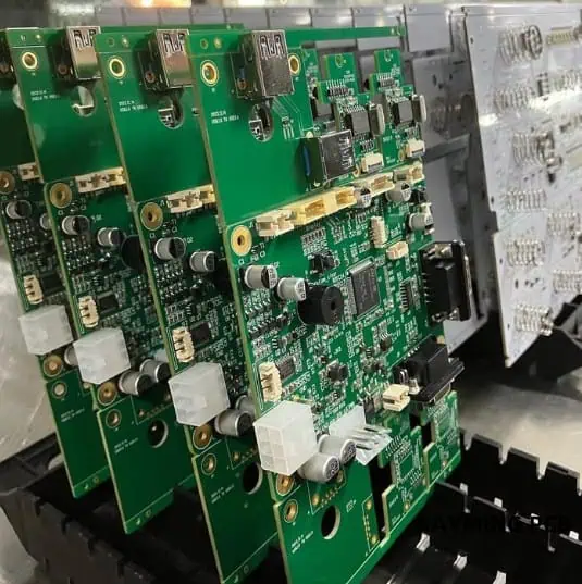
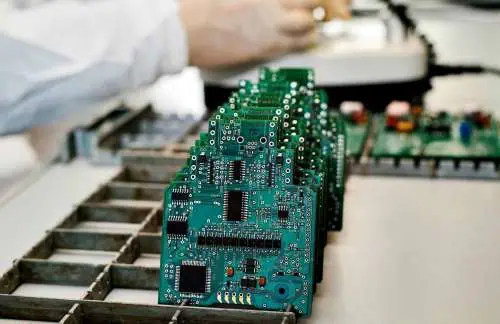
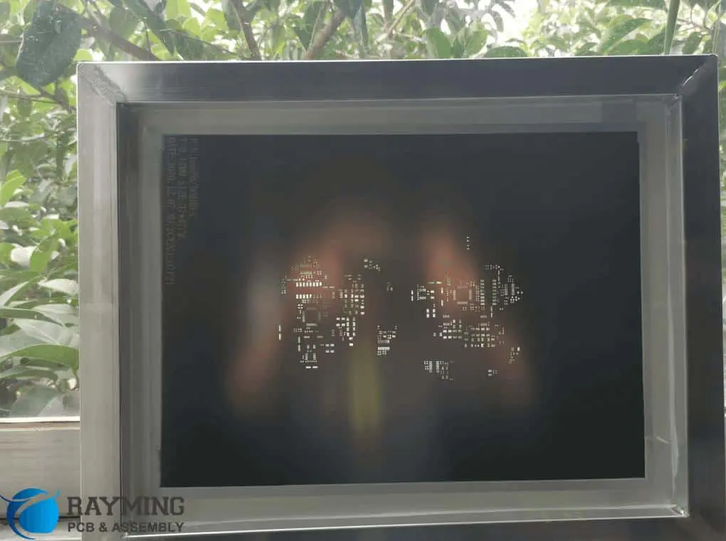
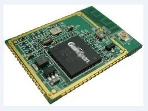
Printed circuit board (PCB) assembly involves soldering and assembling electronic components onto fabricated PCBs using surface mount technology (SMT) and/or through-hole assembly processes. As products become more complex and miniaturized, PCB assembly requires advanced technical capabilities, stringent process controls and quality checks.

China has emerged as a global electronics manufacturing hub with an expansive PCB assembly industry catering to diverse end markets and geographies. This article highlights the top 10 premier PCB assembly manufacturers in China based on factors like production expertise, quality systems, capacity, customer service and value.

Overview of PCB Assembly Process

FULL PCB MANUFACTURING Quote

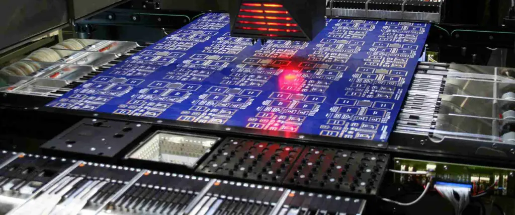
The typical SMT assembly process involves the following key steps:

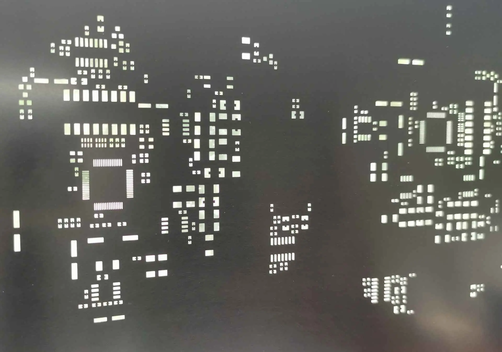
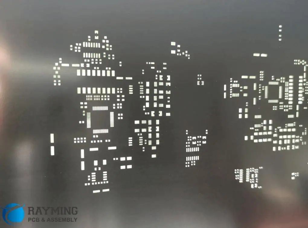
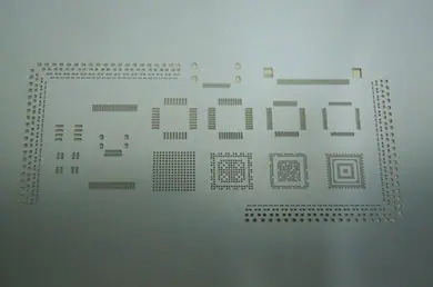
  • Solder Paste Printing – Solder paste is applied on PCB pads where components will be placed to form solder joints post reflow. Stencils control solder deposition.
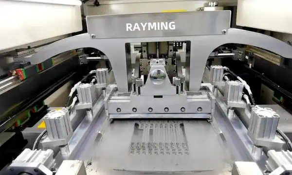
  • SMT Pick and Place – Surface mount components are picked from reels/trays by high-speed pick-place machines and accurately placed on target pads.
  • Reflow Soldering – The PCB travels through a convection reflow oven heating the board. The solder paste melts, fuses and solidifies to form solder joints securing components.
  • Cleaning – Flux residues left after soldering are cleaned using systems like batch cleaning.
  • Inspection – Automated optical inspection (AOI) systems check for defects in solder joint quality or component placement accuracy.
  • Testing – Electrical tests validate boards for correct functionality adhering to IPC standards. Common tests include in-circuit (ICT), flying probe, boundary scan.
  • Conformal Coating – A protective plastic coating may be applied on the assembled board surfaces.

For through-hole assembly, leads are inserted into plated holes in boards either manually or by automated insertion, then wave soldered.

Rigorous process controls and testing ensures reliable, high-yield PCB assemblies. Premier manufacturers invest in advanced automation, inspection and quality systems.

Benefits of Outsourcing PCB Assembly to China

Here are some of the major advantages of outsourcing PCB assembly to China:

Cost Savings

  • Lower labor costs compared to Western countries
  • Highly competitive vendor market drives down pricing
  • Reduced logistics costs due to availability of components locally

Production Expertise

  • Skilled engineering workforce adept in assembly processes
  • Extensive experience across diverse, complex product assemblies
  • Technologically advanced manufacturing equipment and processes

Quality

  • Many manufacturers certified to IPC Class 2 and 3 standards
  • Rigorous quality control and inspection systems
  • Strong focus on process improvement and quality

Capacity

  • Massive production capacity across thousands of assembly facilities
  • Ability to scale easily from prototypes to high-volume production

Supply Chain

  • Close proximity to upstream PCB fabricators and component suppliers
  • Local sourcing of passive components, connectors etc.

Service

  • Strong emphasis on customer service and technical support
  • Responsiveness to quote and design turnaround requests
  • Communication and IP protection mechanisms

By selecting the right partner, companies can leverage China’s PCB assembly capabilities, capacity flexibility and cost advantages while ensuring quality standards.

Top 10 PCB Assembly Manufacturers in China

1. RayMing Technology

RayMing-PCB-and-Assembly

Founded in 2005, RayMing Technology is a leading technologically advanced PCB solutions provider with over 500 employees globally.

Key capabilities:

  • SMT assembly with components as small as 01005 (0.4mm x 0.2mm)
  • 0201 (0.6mm x 0.3mm) chip components assembly
  • Advanced SMT technologies – uBGA, 0.3mm pitch QFN, 0.4mm pitch CSP
  • 12 high-speed SMT assembly lines with 55,000 CPH capability
  • Double-sided, multilayer, HDI, rigid-flex PCB assembly expertise
  • Through-hole, mixed technology assembly support
  • Full functional/ICT/flying probe testing, x-ray inspection
  • Conformal coating, potting, gluing, heat sinking services

RayMing is certified to ISO 9001, ISO 13485, ISO 14001 standards and provides full turnkey assembly solutions from prototyping through volume production for medical, industrial equipment, telecom infrastructure and automotive customers globally.

2. WT Microelectronics

WT Microelectronics is a technologically advanced EMS company providing SMT, through-hole and mixed PCB assembly services from China.

Key capabilities:

  • High-mix, low-volume SMT assembly capabilities
  • 01005 component assembly with 0.2mm pitch
  • BGA, 0.4mm pitch CSP, 0201 and 0.3mm pitch components
  • 9 high-speed SMT assembly lines with 36,000 CPH capacity
  • Double-sided and multilayer PCB assemblies
  • Functional testing, AOI, X-ray inspection, ICT
  • Box build, coating, precision cleaning services

WT Microelectronics provides full assembly solutions including procurement, turnkey NPI, test development and global logistics. They cater to industrial, automotive, and medical OEMs across the world.

3. Hollison Electronics

Hollison provides advanced electronics manufacturing services including PCB assembly from China for global customers since 2000.

Key capabilities:

  • High mix, low-mid volume PCB assembly expertise
  • SMT lines handle BGAs with 0.5mm pitch, 0201 components
  • 9 high-speed SMT assembly lines with 50,000 CPH
  • Testing services include ICT, AOI, flying probe
  • Conformal coating, potting, gluing, heat sinks
  • UL, ISO 9001, ISO 14001, ISO 13485 certifications
  • Full turnkey assembly with procurement, inventory management

Hollison services diverse industries including industrial equipment, automotive electronics, LED lighting, and home appliances using automated assembly technologies for reliable quality.

through-hole assembly process

4. ChuangLian Electronics

ChuangLian Electronics provides advanced SMT and through-hole PCB assembly in China across 8 plants with over 4000 employees.

Key capabilities:

  • High, medium and low volume PCB assembly
  • 90 high-speed SMT lines with 50,000 CPH capacity
  • Assembly down to 01005 components, 0.3mm QFNs, 0.4mm BGAs
  • ICT, AOI, X-ray testing performed post assembly
  • Conformal coating line for protection
  • UL, ISO 9001, ISO 14001, ISO 13485 certified
  • Full procurement, turnkey assembly and order tracking

ChuangLian services diverse customers globally in computing, medical, industrial, communications sectors using automated processes for consistent quality.

5. Shenzhen geomettry electronics Co.Ltd

Geomettry Electronics provides advanced PCB assembly solutions from China with manufacturing facilities in Dongguan and Fuqing.

Key capabilities:

  • Medium to high volume SMT assembly expertise
  • SMT lines handle 0201 discretes and 01005 passives
  • 0.3mm pitch QFNs, 0.4mm pitch CSPs assembly support
  • Functional test, flying probe test capabilities
  • X-ray inspection, AOI, SPI offered
  • ISO 9001 and ISO 13485 quality certified
  • Full procurement, turnkey assembly services

Geomettry focuses on quality and efficient manufacturing of high-mix or low-to-medium volume assemblies for global OEM customers across industries.

6. Shenzhen Zowie Technology

Zowie Technology is an ISO 9001 and ISO 13485 certified electronic manufacturing service providing SMT assembly in China.

Key capabilities:

  • Medium to high volume production support
  • SMT lines handle 01005 discretes and 0.3mm pitch ICs
  • QFPs, CSPs, 0201 capacitors assembly expertise
  • AOI, flying probe, X-ray inspection testing
  • Protection using solder mask, silkscreen, conformal coating
  • Full turnkey assembly with procurement
  • UL certified manufacturing processes

Zowie services customers globally in industrial controls, IoT, telecom infrastructure and medical devices segments requiring high-mix, flexible assembly.

smt assembly equipment

7. EpochSensation EMS

EpochSensation provides end-to-end EMS including PCB assembly in China for customers across consumer, industrial, automotive and medical segments.

Key capabilities:

  • Low to medium volume, high-mix assembly
  • SMT lines handle 01005 to 0402 components
  • uBGAs, QFNs, 0201 LED assembly expertise
  • ICT, flying probe and functional testing
  • AOI, x-ray inspection and SPI offered
  • Conformal coating and related protection
  • UL, ISO 9001, ISO 14001, ISO 13485 certified
  • Full turnkey assembly with procurement

EpochSensation focuses on flexibility in efficiently assembling highly complex, low to medium volume products for reliability.

8. Shenzhen Depue Technology

Depue Technology offers advanced SMT and mixed PCB assembly solutions from China with over 500 employees.

Key capabilities:

  • High mix, low-mid volume assembly expertise
  • SMT lines handle 01005 passives and 0201 actives
  • Optical inspection and X-ray capabilities
  • Rigid, flex, rigid-flex PCB assembly support
  • Functional testing expertise
  • Supply chain and logistics management
  • UL, ISO 9001, ISO 14001, ISO 13485 certified
  • Full box build, precision cleaning assembly

Depue Technology provides full turnkey and new product introduction (NPI) assembly services for industrial, medical and communications segments.

9. Shenzhen Enkson Electronics

Enkson provides advanced electronics manufacturing services from China including PCB assembly, testing and box build.

Key capabilities:

  • Medium to high volume SMT assembly
  • SMT component sizes down to 01005 handled
  • uBGAs, QFNs, 0201 and 0402 passives assembly
  • Triple inspection process – AOI, X-ray, ICT
  • Rigid, flex and rigid-flex assemblies
  • Potting, gluing, heat sink assembly services
  • UL, ISO 9001, ISO 13485, IATF 16949 certified
  • Full procurement, inventory, kitting services

Enkson specializes in quality focused Automotive, Industrial and Medical PCB assemblies.

10. Shenzhen Seaory Technology

Seaory Technology offers high mix PCB assembly solutions from China to customers globally.

Key capabilities:

  • Low to medium volume, high mix assemblies
  • SMT lines handle 01005 to 0402 components
  • uBGAs, 0201 LEDs, QFN components assembly
  • Functional test, flying probe, boundary scan testing
  • X-ray inspection and AOI capabilities
  • Conformal coating, boxing, heat sinking services
  • UL, ISO 9001, ISO 14001, ISO 13485 certified
  • Complete turnkey assembly with procurement

Seaory provides flexible, high-quality assembly solutions catering to Industrial Controls and IoT market segments.

Key Factors for Selecting a PCB Assembly Partner in China

Here are the most important criteria to evaluate when selecting a PCB assembly partner in China:

Technical Expertise

  • Type of assembly technology – SMT, thru-hole, mixed
  • SMT component sizes handled – 01005s, 0201s etc.
  • Fine-pitch component capabilities – uBGAs, QFNs etc.
  • Number of SMT assembly lines and overall capacity
  • Skill in assembling high-complexity PCBs
  • Testing capabilities – ICT, flying probe, functional

Quality

  • Quality certifications – ISO 9001, IPC Class 2 or 3
  • AOI, X-ray inspection and SPI process implementation
  • Process control and monitoring systems
  • Corrective action processes – 8D reporting etc.
  • Quality engineering support and analysis

Volume Flexibility

  • Prototyping to low, medium and high-volume expertise
  • Short-run vs. volume pricing models
  • Changeover process agility between mixed volumes

Service

  • Technical sales engineering support
  • Design for manufacturing (DFM) analysis
  • Procurement and inventory management services offered
  • Programming and test development support

Cost

  • Pricing model – per component, operation charge etc.
  • Geographic labor rate differences
  • Total delivery cost – assembly + logistics
  • Value engineering recommendations

Customer Focus

  • Responsiveness to requests and communication
  • Order tracking transparency and tooling
  • Continuous improvement and feedback processes
  • Program management during product lifecycle
  • Information security and IP protection

By thoroughly evaluating partners on these key parameters, product teams can identify the right PCB assembly partner matching technical needs, quality expectations, volume flexibility, cost targets and ease of doing business.

Key Success Factors for High-Quality PCB Assembly

Here are some of the vital factors that PCB assemblers need to focus on continuously to achieve consistent quality and reliability:

PCB Design

  • Well-defined assembly drawings and documentation
  • DFM review of placements for manufacturability
  • Sufficient test points for validation and debugging

Components

  • Rigorous sourcing processes for certified suppliers
  • Handling and moisture sensitivity controls
  • Proper storage conditions and expiration management

Processes

  • Documented SMT assembly procedures for repeatability
  • Optimization of solder paste printing
  • Thermal profiling to specifications of soldering equipment and materials used
  • Minimizing placement disruptions e.g. mid-batch component loading

Inspection

  • Clearly defined AOI inspection criteria and review
  • X-ray inspection focus on hidden solder joints
  • Solder joint criteria aligned with IPC standards

Testing

  • Validating test fixtures match design regularly
  • Focusing on functionality testing, not only continuity
  • Debugging capability using flying probes

Training

  • Skills development for machine operators on latest assembly technologies
  • Cross-training staff on multiple functions
  • Process knowledge sharing across production teams

Data Analysis

  • Capture and trending of key process performance metrics
  • Root cause analysis of defects and process deviations
  • Correlating inspection, test and field data

By rigorously focusing on each step of the assembly process and driving continuous improvement, premier partners deliver exceptionally high yields with uncompromising quality.

Frequently Asked Questions

Q: What documentation is required from customers for PCB assembly?

Typical documents needed for assembly are:

  • Manufacturing drawings showing component placements
  • BOM listing reference designators, components and sources
  • Gerber, drill, and assembly drawings
  • IPC netlist detailing connectivity
  • Special process instructions e.g. gluing steps
  • Approved vendor lists
  • Test procedures

Q: How is component procurement handled for PCB assembly?

There are three approaches:

  1. Customer supplies components
  2. Manufacturer procures components
  3. Manufacturer makes recommendations, customer procures

Supplying excess component quantities upfront avoids lead time delays. Some assemblers stock common components.

Q: What manufacturing defects can be detected during PCBA inspection?

AOI inspection finds issues like:

  • Missing or skewed components
  • Insufficient or excess solder
  • Solder balls/bridges
  • PCB damage
  • Foreign object debris

X-ray catches phenomena like:

  • Head-in-pillow
  • Voids in QFN/BGA joints
  • Misalignments under components
  • Broken joints and lifts

Q: How is the PCBA prototyping process different from production?

Prototyping involves more close collaboration between engineers on:

  • Design reviews to resolve manufacturability issues
  • Procurement of small component quantities
  • Testing via debug points vs. test fixtures
  • Incremental build approach to check key functions
  • Additional inspection points to characterize assembly
  • Version control of BOMs, drawings, software

The focus is on flexibility, validation, quality characterization and learning.

Q: What key data should be tracked for process control?

Key PCBA metrics to track include:

  • Assembly yields – SMT, thru-hole, box build
  • Workmanship defects from AOI
  • Test yields and failure pareto
  • Process parameters like solder paste volumes
  • Down times
  • Supplier quality ratings
  • Field returns and failure analysis

Data drives continuous improvement.

Summary

As products require increased functionality in smaller formats, the PCB assembly process needs to evolve with more precise equipment, smaller component handling capability, better inspection systems and quality focus. China offers a vast range of advanced assembly facilities to address diverse prototyping, low to high-volume PCB assembly needs while delivering quality, service, transparency and program management excellence.

By partnering with the premier manufacturers showcased above, companies around the world can leverage China’s PCB assembly value proposition to achieve technology leadership, quality excellence and cost competitiveness necessary to compete and win globally across many dynamic end markets and applications.

What are Solder Paste Stencils?

LASER STENCIL MANUFACTURER
Solder Paste Stencils

As the electronics technology is advancing, the use of through-hole electronic components is getting out of fashion, and Surface Mount Devices have replaced them. The production of modern components is mostly Surface Mount Technology based.

Consequently, many manufacturers prefer using SMDs based products. When it comes to bulk production, manually soldering each board can be hectic and time-consuming. Besides the quality of each joint matters, even a poor joint can trigger malfunctioning in the product.

YouTube video

Surface Mount Technology Stencils offer convenience in depositing solder paste within perfect quantity and shape. All you need to do is to set up your board, put some solder paste and swipe it. In case of a single prototype to be developed, using an SMT stencil can be costly and, but for bulk production, SMT stencils can considerably reduce production time and cost.

Stencils are usually used in industry for bulk production, and a single stencil can serve thousands of PCBs. However, for few units production, metal stencils can be expensive. For small quantity of units to be produced, polyimide stencils are more suitable. These laser cut stencils works reliably if you are working on a few boards. Since these laser stencils are made of synthetic polymer, and the development cost is low, they are suitable for a limited quantity of boards to be developed.

How are Solder Paste Stencils Designed?

FULL PCB MANUFACTURING Quote

The solder paste stencil is designed using a soft version of the project. During the circuit is designed using any designer software such as Altium, Eagle, DipTrace or Kicad. The soft design includes a layer of solder paste and using this layer machine is instructed to cut holes in exact dimensions are precise locations.

The dimensions and location of each stencil hole determine its efficiency, designing a stencil using original design files of circuit ensure the locations are accurate and the solder paste is deposited in precise dimensions.

Since the solder paste needs to be deposited in a limited region and it can spread slightly out the hole boundaries. To cover up the excessive deposition, the stencil holes are designed a bit smaller the component pads.

How is a Solder Paste Stencil Used?

Using a solder paste stencil is simple and easy. The hardware must be set up properly before deposition, and the PCB needs to be in stationary position, in case of vibrations or movement, the solder paste might be deposited out the pads.

After setting up hardware, the stencil and PCB must be appropriately aligned. The alignment should ensure each solder pad is exposed through the holes of the stencil. Fix stencil on PCB. When aligning the stencil and PCB, look for IC pads, they are easy to track as they have multiple pads.

Carefully verify each pad is exposed through the hole and then put some solder paste on the stencil, using a card, slowly spread solder paste on holes. The paste needs to be spread in all direction to ensure the hole is appropriately covered with paste and the pad is not left uncovered partially.

Solder paste should be used within a few hours of pasting, in case of delay, its efficiency might reduce. Usually, solder paste deposited on stencil is more than needed and the extra paste is used for the next board. It is recommended to use a limited quantity of paste that can be served on a single board.

When the paste has been deposited entirely, remove tapes on the stencil and carefully remove the stencil from the PCB. Inspect each pad, check if the paste has been appropriately deposited. In case, the paste has spread more than needed, it must be removed, and if the paste is missing on any locations, it must be deposited manually.

After the paste is deposited on a PCB, often some paste is left in the stencil holes. This leftover paste is not harmful to the stencil and can be wiped later.

laser cut stencils

Carefully place all components using SMT pick and place machine, ensure the direction of the component is according to the design. Sometimes, during the placement of components, the component is misplaced or disoriented. Such misplacements can cause improper or no soldering of any legs. In such case, carefully move disoriented component and bring it in a proper place. A minute quantity of paste is often spread around the pad during the replacement. But during heating, this paste reaches back to the pad.

After a detailed examination of each component, the PCB is passed through an oven which heats the board from the top and the paste turns into molten solder. The paste is usually in flat formation before heating but as soon as it is heated, it takes the form of a proper solder joint, and the corresponding componentโ€™s leg is soldered with the pad.

Solder paste deposition demands patience and practice. The procedure is easy, but the process needs to be handled carefully.

Solder Paste Stencils manufacturing at RAYMING

RAYMING is a top notch seller of a variety of solder paste stencils. It doesnโ€™t matter if you belong to a small or large industry with a few or several units order, RAYMING will come up with an affordable offer for you.

We offer various services related to prototype PCB assembling. The modern technologies and state of the art machinery at RAYMING labs maintain superior quality of our services. So far, we have assisted industries belonging to different segments of the market, and we have developed a name for quality services.

We understand that the product reliability and durability are the core qualities that should not be compromised at any cost. Our automated systems enable us to focus even on microscopic level details of products.

Product development with proper testing makes it reliable and builds the confidence of consumer in using it. We, as a manufacturer of solder paste stencils, test each stencil on our advanced systems and our team ensures the product quality is maintained according to international standards.

RAYMING cares about small industries, and it has played a significant role in uplifting small industries. If you are looking for a PCB stencil manufacturer, share your order details, and we will offer an appealing package.

We are always open to queries, if you need support, contact us at sales@raypcb.com and you will be responded in a short time.

Quick Turn PCB Assembly: Speed Without Compromise

pcb assembly cost down

In today’s fast-paced electronics industry, time-to-market is crucial for staying competitive. Quick turn PCB assembly has emerged as a game-changer, allowing companies to rapidly prototype and produce small batches of printed circuit boards without sacrificing quality. This article delves into the world of quick turn PCB assembly, exploring its benefits, processes, and how to choose the right partner for your needs.

What is Quick Turn PCB Assembly?

Quick turn PCB assembly refers to the rapid production of printed circuit boards, typically for prototyping or small production runs. This service emphasizes speed and efficiency without compromising on quality or reliability. Quick turn assembly involves expedited processes at every stage, from design review to component procurement and final assembly.

Key Features of Quick Turn PCB Assembly:

  • Accelerated turnaround times
  • Flexible production quantities
  • Advanced manufacturing technologies
  • Streamlined communication and project management
  • Rigorous quality control measures

Learn more about:

Benefits of Quick Turn PCB Assembly Orders

Opting for quick turn PCB assembly offers numerous advantages for businesses across various industries. Let’s explore the key benefits:

1. Faster Time-to-Market

In today’s competitive landscape, being first to market can make all the difference. Quick turn PCB assembly significantly reduces production time, allowing you to:

  • Launch products ahead of competitors
  • Capitalize on market opportunities
  • Respond rapidly to customer demands

2. Cost-Effective Prototyping

Quick turn assembly enables efficient prototyping, which can lead to substantial cost savings:

  • Identify and resolve design issues early
  • Reduce the need for multiple revision cycles
  • Minimize waste and material costs

3. Flexibility in Design Iterations

The ability to quickly produce and test prototypes allows for greater flexibility in the design process:

  • Easily implement design changes
  • Experiment with different components or layouts
  • Optimize performance before full-scale production

4. Improved Quality Control

Despite the emphasis on speed, quick turn PCB assembly maintains high-quality standards:

  • Catch and correct errors early in the production process
  • Ensure functionality and reliability of the final product
  • Meet industry-specific quality requirements

5. Enhanced Customer Satisfaction

By reducing lead times and improving product quality, quick turn assembly leads to:

  • Faster delivery of products to end-users
  • Increased customer trust and loyalty
  • Competitive advantage in the market

How to Get Quick Turn PCBAs?

Securing quick turn PCB assembly services involves several key steps:

  1. Prepare Your Design Files: Ensure your PCB design files are complete and error-free.
  2. Choose a Reliable Partner: Select a PCB assembly service provider with a track record of quick turnaround and quality results.
  3. Submit Your Order: Provide all necessary information, including design files, bill of materials (BOM), and any special requirements.
  4. Review and Approve: Quickly review and approve any design for manufacture (DFM) feedback or quotations.
  5. Track Your Order: Stay in close communication with your assembly partner throughout the process.

What is Considered a Quick Turn for PCB Assembly?

The definition of “quick turn” can vary depending on the complexity of the PCB and the capabilities of the assembly partner. However, general guidelines include:

  • Prototypes: 24-72 hours
  • Small Production Runs: 3-5 business days
  • Medium Production Runs: 5-10 business days

It’s important to note that these timeframes can be influenced by factors such as board complexity, component availability, and specific customer requirements.

RAYMING’s Typical Turnaround Time for Quick Turn PCB Assembly

At RAYMING, we pride ourselves on our ability to deliver high-quality PCBAs with industry-leading turnaround times. Our typical quick turn assembly timeframes are:

  • Prototype PCBAs: As fast as 72hours
  • Small Production Runs (1-100 units): 5-8 business days
  • Medium Production Runs (101-500 units): 10-15 business days

These timelines showcase our commitment to speed without compromising on quality or reliability.

Factors that Affect the Turnaround Time of a Prototype

Several factors can impact the turnaround time for quick turn PCB assembly:

1. PCB Complexity

  • Number of layers
  • Board size and shape
  • Component density

2. Component Availability

  • Standard vs. specialized components
  • Lead times for specific parts
  • Alternative component options

3. Assembly Requirements

4. Testing and Quality Assurance

  • Level of testing required
  • Compliance with industry standards
  • Documentation needs

5. Production Volume

  • Prototype vs. small-batch production
  • Scalability of assembly processes

Understanding these factors can help you work more effectively with your assembly partner to achieve the fastest possible turnaround times.

What is the Quick Turn PCB Assembly Process?

The quick turn PCB assembly process involves several key stages, each optimized for speed and efficiency:

1. Design Review and DFM Analysis

  • Rapid assessment of PCB design files
  • Identification of potential manufacturing issues
  • Quick feedback and design optimization suggestions

2. Component Procurement

  • Fast sourcing of required components
  • Utilization of extensive supplier networks
  • Strategic inventory management for common parts

3. PCB Fabrication

  • High-speed PCB manufacturing processes
  • Advanced equipment for quick board production
  • Rigorous quality control checks

4. Component Placement

  • Automated pick-and-place machines for SMT components
  • Skilled technicians for through-hole component insertion
  • Optimized production line setup for efficiency

5. Soldering

6. Inspection and Testing

  • Automated optical inspection (AOI)
  • X-ray inspection for hidden solder joints
  • Functional testing as per customer requirements

7. Quality Assurance and Packaging

  • Final quality checks and documentation
  • Secure packaging for safe transportation
  • Rapid shipping arrangements

By streamlining each of these stages, quick turn PCB assembly providers can deliver high-quality boards in record time.

Choosing the Right Quick Turn Assembly Partner in China

Selecting the right quick turn PCB assembly partner in China is crucial for the success of your project. Consider the following factors:

1. Experience and Expertise

  • Years in the industry
  • Range of PCB assembly capabilities
  • Industry-specific knowledge

2. Technology and Equipment

  • State-of-the-art assembly equipment
  • Advanced inspection and testing technologies
  • Continuous investment in new capabilities

3. Quality Certifications

  • ISO 9001 certification
  • IPC standards compliance
  • Industry-specific certifications (e.g., AS9100 for aerospace)

4. Communication and Customer Service

  • English-speaking support staff
  • 24/7 availability
  • Transparent and responsive communication

5. Flexibility and Scalability

  • Ability to handle various order sizes
  • Quick adaptation to design changes
  • Scalability for future production needs

6. Intellectual Property Protection

  • Robust IP protection policies
  • Confidentiality agreements
  • Secure data handling practices

7. Cost-Effectiveness

  • Competitive pricing
  • Value-added services
  • Transparent quotation process

Why Should You Choose RAYMING as Your Preferred Partner?

RAYMING stands out as a leading quick turn PCB assembly partner in China for several compelling reasons:

1. Unparalleled Expertise

With over 15 years of experience in the PCB industry, RAYMING has developed deep expertise in quick turn assembly across various sectors, including automotive, aerospace, medical, and consumer electronics.

2. Cutting-Edge Technology

We invest continuously in the latest assembly equipment and technologies, ensuring that we can handle even the most complex PCB designs with speed and precision.

3. Rigorous Quality Control

Our ISO 9001-certified facilities and adherence to IPC standards guarantee that every PCBA we produce meets the highest quality standards, regardless of the turnaround time.

4. Customer-Centric Approach

We pride ourselves on our responsive customer service, with dedicated project managers ensuring clear communication and rapid resolution of any issues throughout the assembly process.

5. Flexible and Scalable Services

Whether you need a single prototype or a production run of thousands, RAYMING can adapt to your requirements, providing consistent quality and speed at any scale.

6. Comprehensive Capabilities

From design review to final testing and packaging, we offer end-to-end PCB assembly services, streamlining your supply chain and reducing time-to-market.

7. Competitive Pricing

Our efficient processes and strategic location in China allow us to offer highly competitive pricing without compromising on quality or speed.

Conclusion

Quick turn PCB assembly has revolutionized the electronics manufacturing industry, enabling companies to bring products to market faster than ever before. By choosing the right assembly partner, you can leverage this powerful service to gain a competitive edge, reduce costs, and improve product quality.

RAYMING’s commitment to speed, quality, and customer satisfaction makes us the ideal choice for your quick turn PCB assembly needs. Whether you’re a startup looking to prototype your first product or an established company seeking to optimize your production process, we have the expertise and capabilities to exceed your expectations.

Don’t let slow turnaround times hold your projects back. Experience the RAYMING difference in quick turn PCB assembly today. Contact us to discuss your PCB assembly needs and discover how we can help accelerate your time-to-market without compromising on quality.

High-Quality PCB Stencils for Accurate Solder Paste Printing

Stencil Electronics

In the world of printed circuit board (PCB) manufacturing, precision is paramount. One crucial tool that ensures accuracy in the assembly process is the PCB stencil. This article delves into the intricacies of PCB stencils, exploring their composition, types, manufacturing processes, and how to choose and use them effectively.

What is a PCB Stencil?

A PCB stencil is a thin sheet of material with precisely cut openings that allow for the accurate application of solder paste onto specific areas of a printed circuit board. This tool is essential in the surface mount technology (SMT) assembly process, where components are soldered directly onto the surface of the PCB.

Key functions of a PCB stencil include:

  • Ensuring precise solder paste deposition
  • Controlling the volume of solder paste applied
  • Maintaining consistency across multiple boards
  • Improving the efficiency of the PCB assembly process

The use of high-quality PCB stencils is crucial for achieving reliable solder joints, reducing defects, and enhancing the overall quality of electronic products.

Learn more about:

What is a PCB Stencil Made Of?

laser stencil pcb

A PCB stencil consists of several components, each playing a vital role in its functionality and durability. Let’s examine the main elements:

1. Frame

The frame provides structural support for the stencil and helps maintain its shape during use. Frames can be:

  • Aluminum: Lightweight and cost-effective
  • Stainless Steel: Durable and resistant to warping
  • Tubular: Offers enhanced stability for larger stencils

2. Steel Sheet

The steel sheet is the primary component of the stencil, containing the precisely cut apertures for solder paste application. Common materials include:

  • Stainless Steel: Most widely used due to its durability and resistance to corrosion
  • Nickel: Offers excellent release properties and is suitable for fine-pitch applications
  • Brass: Used in some specialized applications

The thickness of the steel sheet typically ranges from 0.1mm to 0.2mm, depending on the specific requirements of the PCB design.

3. Mesh

Some stencils incorporate a mesh material to provide additional support and prevent sagging. The mesh is typically made of:

  • Polyester: Offers good tension and durability
  • Stainless Steel: Provides excellent strength and heat resistance

4. Glue

Adhesive is used to attach the steel sheet to the frame and, if present, the mesh. The glue must be:

  • Strong enough to withstand repeated use
  • Resistant to cleaning solvents used in the PCB assembly process
  • Able to maintain its properties under varying temperature conditions

Types of PCB Stencils

smd stencil

PCB stencils come in various types, each suited for different applications and production requirements. Let’s explore the main categories:

1. Framed SMT/PCB Stencil

Framed stencils are the most common type used in PCB assembly. They consist of a steel sheet mounted on a rigid frame.

Advantages:

  • Excellent stability during printing
  • Easy to handle and store
  • Suitable for high-volume production

Disadvantages:

  • Higher cost compared to frameless options
  • Requires more storage space

2. Frameless SMT Stencil

Also known as foil stencils, these are flexible sheets without a permanent frame.

Advantages:

  • Cost-effective for low-volume production
  • Easy to store and transport
  • Can be used with adjustable tension frames

Disadvantages:

  • Requires careful handling to prevent damage
  • May not be as stable as framed stencils during printing

3. Electroformed SMT Stencil

Electroformed stencils are created through an electroplating process, resulting in extremely precise apertures.

Advantages:

  • Ideal for ultra-fine pitch applications
  • Excellent release properties
  • Smooth aperture walls for consistent solder paste release

Disadvantages:

  • Higher cost compared to other types
  • Limited thickness options

How are Stencils Manufactured?

YouTube video

The manufacturing process of PCB stencils plays a crucial role in their quality and performance. There are three main methods used to create stencils:

1. Chemical Etching

Chemical etching is a traditional method that involves using chemicals to dissolve away unwanted material from the stencil sheet.

Process:

  1. Apply a protective mask to the stencil material
  2. Expose the mask to UV light through a photographic negative of the stencil design
  3. Remove the unexposed areas of the mask
  4. Immerse the sheet in an etching solution to remove exposed metal
  5. Clean and inspect the finished stencil

Advantages:

  • Cost-effective for simple designs
  • Suitable for prototype and low-volume production

Disadvantages:

  • Limited precision for very fine pitch applications
  • Can result in slightly tapered aperture walls

2. Laser Cutting

Laser cutting is the most widely used method for PCB stencil manufacturing due to its precision and versatility.

Process:

  1. Load the stencil material into the laser cutting machine
  2. Input the stencil design data
  3. The laser beam cuts the apertures with high precision
  4. Clean and inspect the finished stencil

Advantages:

  • High accuracy and repeatability
  • Suitable for fine-pitch and complex designs
  • Fast turnaround time

Disadvantages:

  • Higher initial equipment cost
  • Potential for heat-affected zones around apertures

3. Electroforming

Electroforming is a specialized process that creates stencils by growing metal around a mandrel.

Process:

  1. Create a mandrel with the inverse of the desired stencil pattern
  2. Immerse the mandrel in an electroplating bath
  3. Apply an electric current to deposit metal onto the mandrel
  4. Remove the formed stencil from the mandrel
  5. Clean and inspect the finished stencil

Advantages:

  • Extremely precise apertures with smooth walls
  • Ideal for ultra-fine pitch applications
  • Excellent solder paste release properties

Disadvantages:

  • Higher cost compared to other methods
  • Limited to thinner stencil options

How to Choose the Correct PCB Stencil?

Selecting the right PCB stencil is crucial for achieving optimal solder paste deposition. Consider the following factors when choosing a stencil:

1. Stencil Thickness

The thickness of the stencil determines the volume of solder paste deposited. Common thicknesses include:

  • 0.1mm (4 mil): For ultra-fine pitch components
  • 0.12mm (5 mil): Suitable for most SMT applications
  • 0.15mm (6 mil): For larger components or high-power applications

Factors influencing thickness choice:

  • Component lead pitch
  • Pad size and shape
  • Required solder volume

2. Aperture Size of the Created Opening

The size and shape of the apertures affect solder paste release and deposit accuracy.

Considerations:

  • Aspect ratio (aperture width to stencil thickness)
  • Area ratio (aperture area to aperture wall area)
  • Minimum aperture size based on manufacturing method

3. Stencil Material

The choice of material impacts the stencil’s durability and performance.

Options:

  • Stainless Steel: Most common, suitable for most applications
  • Nickel: Excellent for fine-pitch and step stencils
  • Polyimide: Used for flexible stencils in prototype applications

4. Stencil Alignment

Proper alignment ensures accurate solder paste deposition.

Alignment methods:

  • Fiducial marks: For automated alignment systems
  • Tooling holes: For manual alignment fixtures
  • Stencil borders: For visual alignment in prototype applications

How to Use a PCB Stencil

Using a PCB stencil effectively requires attention to detail and proper technique. Follow these steps for optimal results:

  1. Prepare the PCB: Ensure the board is clean and properly secured.
  2. Set up the stencil printer:
    • Adjust the printer’s parameters (speed, pressure, separation speed)
    • Align the stencil with the PCB using fiducials or tooling holes
  3. Apply solder paste:
    • Place an appropriate amount of solder paste on the stencil
    • Use the squeegee to spread the paste across the stencil surface
  4. Perform the print stroke:
    • Move the squeegee across the stencil at a consistent speed and pressure
    • Ensure complete filling of all apertures
  5. Separate the stencil:
    • Lift the stencil from the PCB at a controlled speed
    • Avoid smearing or disturbing the deposited solder paste
  6. Inspect the result:
    • Visually check for consistent solder paste deposits
    • Use automated inspection systems for high-volume production
  7. Clean the stencil:
    • Remove excess solder paste after each use
    • Use appropriate cleaning solutions and methods

Tips for optimal stencil use:

  • Maintain consistent room temperature and humidity
  • Regularly inspect the stencil for damage or wear
  • Follow manufacturer recommendations for stencil care and storage

Prices of PCB Stencils

The cost of PCB stencils can vary widely depending on several factors:

  1. Stencil Type:
    • Framed stencils:ย 100โˆ’100โˆ’300
    • Frameless stencils:ย 50โˆ’50โˆ’150
    • Electroformed stencils:ย 200โˆ’200โˆ’500+
  2. Size:
    • Small (up to 10″ x 10″):ย 75โˆ’75โˆ’150
    • Medium (10″ x 10″ to 20″ x 20″):ย 150โˆ’150โˆ’300
    • Large (over 20″ x 20″):ย 300โˆ’300โˆ’500+
  3. Material:
    • Stainless Steel: Standard pricing
    • Nickel: 10-20% premium over stainless steel
    • Polyimide: Variable, often used for prototyping
  4. Manufacturing Method:
    • Laser-cut: Standard pricing
    • Chemical etched: Often lower cost for simple designs
    • Electroformed: Premium pricing for high-precision requirements
  5. Turnaround Time:
    • Standard (3-5 business days): Base price
    • Rush (1-2 business days): 25-50% premium
    • Same-day: 50-100% premium (where available)
  6. Design Complexity:
    • Simple designs: Base price
    • Complex designs with many small apertures: 10-30% premium
  7. Quantity:
    • Single stencil: Base price
    • Multiple stencils of the same design: Discounts often available
  8. Additional Features:
    • Nano-coating for improved release:ย 20โˆ’20โˆ’50 premium
    • Step stencils: 20-40% premium over standard stencils

When requesting quotes for PCB stencils, provide detailed specifications to ensure accurate pricing. Many manufacturers offer online quoting tools for instant estimates based on your specific requirements.

Conclusion

High-quality PCB stencils are essential for achieving accurate and consistent solder paste application in PCB assembly. By understanding the types of stencils available, their manufacturing processes, and how to choose and use them effectively, you can significantly improve the quality and reliability of your electronic products.

When selecting a PCB stencil supplier, consider factors such as manufacturing capabilities, quality control processes, and customer support. Look for providers who offer design assistance and can accommodate your specific requirements, whether you’re working on prototypes or high-volume production runs.

Investing in the right PCB stencil can lead to:

  • Improved solder joint quality
  • Reduced defect rates
  • Enhanced production efficiency
  • Consistent results across multiple boards

By carefully considering your PCB design, production requirements, and budget, you can choose the optimal stencil solution for your project. Remember that while the initial cost of a high-quality stencil may be higher, the long-term benefits in terms of improved product quality and reduced rework often outweigh the investment.

As PCB designs continue to evolve with finer pitches and more complex layouts, the role of precision stencils in the assembly process becomes increasingly critical. Stay informed about the latest developments in stencil technology and manufacturing techniques to ensure your PCB assembly process remains at the cutting edge of quality and efficiency.

PCB Assembly Cost in 2026: Complete Pricing Guide + Calculator

pcb assembly cost down

If you’ve ever opened a quote from a contract manufacturer and felt your stomach drop, you’re not alone. PCB assembly cost remains one of the most confusing aspects of electronics manufacturing, with prices ranging anywhere from $0.02 to over $100 per board. After 15 years of designing boards and working with dozens of assembly houses across three continents, I’ve learned that understanding where your money goes is half the battle.

This guide breaks down exactly what drives PCB assembly cost in 2026, gives you real pricing data from actual production runs, and shows you practical ways to cut expenses without sacrificing quality. Whether you’re prototyping your first IoT device or scaling to 10,000-unit production runs, you’ll walk away knowing how to budget accurately and negotiate smarter.

Quick Answer: What Does PCB Assembly Cost in 2026?

Before we dive deep, here’s what you can expect to pay right now:

Production VolumeCost Per BoardTypical Use Case
Prototype (1-10 pcs)$50 – $200+Design validation, investor demos
Small Batch (10-100 pcs)$20 – $80Beta testing, initial customers
Mid Volume (100-1,000 pcs)$10 – $50Product launch, market entry
High Volume (1,000-10,000 pcs)$5 – $25Established products
Mass Production (10,000+ pcs)$2 – $15Consumer electronics

These figures include PCB fabrication, component placement, and basic testing. Your actual cost depends on board complexity, component selection, and turnaround timeโ€”factors we’ll examine in detail below.

PCB Assembly Cost Calculator | RAYPCB Engineering Tools
๐Ÿ› ๏ธ Engineering Tools

PCB Assembly Cost Calculator

Estimate your PCB and PCBA project costs accurately. Get instant pricing for fabrication, components, assembly, and testing.

PCB Specifications

Step 1
mm
mm

Components & BOM

Step 2
USD

Assembly Options

Step 3

๐Ÿ’ก Cost-Saving Tips

โ€ข Increase quantity to reduce per-board cost (setup fees are amortized)
โ€ข Choose standard turnaround to avoid rush premiums
โ€ข Minimize BGA/QFN parts to reduce X-ray inspection costs
โ€ข Use standard FR-4 material when possible

Cost Estimate

Estimated Total Cost
$0.00
Per Board: $0.00
PCB Fabrication
$0.00
Components (BOM)
$0.00
SMT/THT Assembly
$0.00
Testing & QC
$0.00
Setup & Engineering
$0.00

Understanding the PCB Assembly Cost Formula

Every assembly quote you receive breaks down into four major buckets. Miss any one of them, and your budget projections will be off.

The Four Cost Pillars

PCB Assembly Cost = Fabrication + Components + Assembly Labor + Testing/Overhead

Let me show you how this plays out with a real example. Last quarter, I worked on a 4-layer IoT sensor board (100mm ร— 80mm) with 127 components. Here’s the actual cost breakdown for a 500-unit run:

Cost CategoryAmount% of Total
PCB Fabrication$1,250 ($2.50/board)18%
Components$3,500 ($7.00/board)50%
SMT Assembly$1,750 ($3.50/board)25%
Testing & QC$500 ($1.00/board)7%
Total$7,000 ($14.00/board)100%

Notice that components ate up half the budget. This is typical for mid-complexity designs. On simpler boards, fabrication takes a larger share; on complex designs with expensive ICs, components can hit 70% or more.

Factors That Drive PCB Assembly Cost Up (or Down)

After analyzing quotes from over 40 assembly houses, I’ve identified the factors that actually move the needle on pricing. Some will surprise you.

Board Complexity and Layer Count

Layer count is the single biggest driver of fabrication cost. The relationship isn’t linearโ€”it’s exponential.

Layer CountRelative CostTypical Applications
1-2 layers1x (baseline)Simple consumer products, LED drivers
4 layers2-2.5xIoT devices, most consumer electronics
6 layers3-4xIndustrial controls, RF applications
8 layers5-6xNetworking equipment, high-speed digital
10+ layers8-12xServers, telecom infrastructure

Engineer’s Tip: Before adding layers, ask yourself if better component placement or routing optimization could solve your signal integrity issues. I’ve seen engineers request 6-layer boards when clever ground plane design on 4 layers would have worked fine.

Component Selection and Availability

Your BOM (Bill of Materials) decisions made months ago now determine your assembly cost. Here’s what I’ve learned to watch for:

Standard vs. Specialized Components

Component TypePrice RangeAssembly Complexity
0402/0603 Resistors, Capacitors$0.001 – $0.01Low
Standard ICs (SOIC, TSSOP)$0.10 – $5.00Low to Medium
QFN/LGA Packages$0.50 – $15.00Medium (requires X-ray)
BGA Packages$2.00 – $50.00+High (requires X-ray)
Fine-pitch (โ‰ค0.4mm) ComponentsVariesHigh (precision placement)

BGAs and QFNs aren’t just more expensive to buyโ€”they cost more to assemble because they require X-ray inspection. Every BGA on your board might add $0.50-$2.00 to your per-board inspection cost.

The 2026 Component Availability Reality

We’re still feeling aftershocks from the 2020-2023 chip shortage. In 2026, I’m seeing:

  • MCU prices stabilized but still 10-15% above 2019 levels
  • Passive components mostly normalized
  • Power management ICs remain tight in some families
  • Lead times for automotive-grade parts still extended

When a component goes into allocation, assembly houses charge premium rates for sourcing. I’ve seen quotes jump 30% because one IC needed to be sourced from the secondary market.

Assembly Method: SMT vs. Through-Hole

The assembly method you need significantly impacts your PCB assembly cost. Here’s the real-world comparison:

Assembly TypeCost per PlacementBest For
SMT (Machine)$0.001 – $0.02High-volume, standard components
SMT (Manual)$0.03 – $0.08Prototypes, odd-form parts
Through-Hole (Wave)$0.02 – $0.05Connectors, high-power components
Through-Hole (Manual)$0.05 – $0.15Low volume, mixed technology
Mixed TechnologyAdd 20-40%When you need both

My Rule of Thumb: Every through-hole component you can eliminate saves money twiceโ€”once on component cost (SMT parts are usually cheaper) and again on assembly cost. But don’t compromise mechanical strength for connectors that will see physical stress.

Understanding SMT Placement Pricing

Most CMs calculate SMT pricing based on “placement points” or “solder joints.” A simple 0603 resistor counts as 2 points (one per pad), while a 100-pin QFP counts as 100 points. This is why high-pin-count ICs can dramatically increase your assembly cost even though they’re just one component.

Here’s how different component types affect your placement costs:

Component PackagePoints per PartTypical Handling Fee
0201 passives2+$0.01 (precision placement)
0402/0603/0805 passives2Standard rate
SOIC, TSSOP, QFPPin countStandard rate
Fine-pitch (โ‰ค0.5mm)Pin count+$0.02-0.05 per part
BGA (any pitch)Ball count+$0.10-0.50 per part + X-ray
QFN/LGAPad count+$0.05-0.20 per part + X-ray

The Double-Sided Assembly Premium

If your design requires components on both sides of the board, expect to pay 50-80% more than single-sided assemblyโ€”not double. The reason is that the second pass through the reflow oven uses the same stencil setup, so you’re mainly paying for additional pick-and-place time and the second reflow cycle.

However, double-sided designs with heavy components on the bottom side may require selective soldering or special fixtures, which can add significant cost. I once had a project where bottom-side capacitors kept falling off during the second reflowโ€”we ended up redesigning to keep all heavy components on top.

Order Quantity and Economies of Scale

This is where many engineers get burned during budgeting. Setup costs don’t scale with quantity.

One-Time CostsTypical Range
SMT Stencil$30 – $150
Pick-and-Place Programming$50 – $200
First Article Inspection$100 – $300
Test Fixture (if needed)$200 – $2,000+

For a 10-board prototype run with $300 in setup fees, you’re adding $30/board before any actual assembly happens. At 1,000 boards, that same setup cost adds just $0.30/board.

Real Pricing Example by Volume:

QuantitySetup (amortized)AssemblyComponentsTotal/Board
5 pcs$60.00$15.00$12.00$87.00
50 pcs$6.00$8.00$10.00$24.00
500 pcs$0.60$4.00$8.00$12.60
5,000 pcs$0.06$2.50$6.50$9.06

Turnaround Time Premium

Need boards fast? You’ll pay for it.

TurnaroundPrice PremiumWhen to Use
Standard (10-15 days)BaselineProduction runs, planned builds
Expedited (5-7 days)+30-50%Product launches, deadline pressure
Rush (3-5 days)+75-150%Critical fixes, trade shows
Super Rush (24-72 hrs)+200-300%Emergency only

I’ve paid rush fees exactly twice in my career, both times for trade show demos. Every other time, better planning would have saved thousands.

Geographic Location of Assembly

Where your boards get built matters enormously for PCB assembly cost.

RegionCost LevelProsCons
China (Shenzhen)LowestPrice, speed, capacityIP concerns, shipping time
Southeast AsiaLow-MediumGrowing quality, good priceLess mature supply chain
Eastern EuropeMediumQuality, EU proximitySmaller capacity
USA/Western EuropeHighestIP protection, communication2-5x China pricing

My Approach: I use Chinese assembly for consumer products and anything that’s not IP-sensitive. For defense, medical, or truly novel designs, I pay the premium for domestic assembly.

How to Calculate Your PCB Assembly Cost

Let me walk you through the calculation process I use for every project. Getting this right prevents budget surprises and helps you make informed design tradeoffs.

Step 1: Gather Your Design Data

Before requesting quotes, have these ready:

  • Gerber files (RS-274X format)
  • Bill of Materials with manufacturer part numbers
  • Pick-and-place/centroid file
  • Assembly drawings (PDF)
  • Special instructions (conformal coating, programming, etc.)

A Word About BOM Preparation

Your BOM quality directly affects quote accuracy. A poorly formatted BOM forces the CM to make assumptionsโ€”assumptions that often favor their margins, not yours. Include:

  • Manufacturer Part Number (MPN) for every component
  • Approved alternates when available
  • Reference designators matching your centroid file
  • Quantity per board (not total quantity)
  • Package/footprint information

I use a standardized BOM template that I’ve refined over years. It includes columns for primary MPN, alternate 1, alternate 2, and notes. This flexibility lets CMs find the best pricing without requiring your approval for every substitution.

Step 2: Use This Estimation Formula

For quick budgeting before formal quotes, use this formula:

Estimated Cost = (PCB ร— Qty) + (Comp ร— Qty) + Setup + (Placement ร— Points ร— Qty) + Testing

Where:
- PCB = Bare board cost ($0.50-$5.00 for standard boards)
- Comp = Total BOM cost per board
- Setup = $100-$400 depending on complexity
- Placement = $0.01-$0.05 per point (SMT) or $0.05-$0.15 (THT)
- Points = Number of solder joints (roughly 2ร— component count for dual-row ICs)
- Testing = $0.10-$5.00 per board depending on requirements

Step 3: Sample Cost Calculation

Let’s calculate for a medium-complexity board:

Board Specs:

  • 4-layer, 100mm ร— 100mm
  • 150 SMT components (300 solder points)
  • 10 through-hole components (20 solder points)
  • BOM cost: $15/board
  • Quantity: 200 units

Calculation:

  • PCB Fabrication: $2.00 ร— 200 = $400
  • Components: $15.00 ร— 200 = $3,000
  • Setup (stencil + programming): $200
  • SMT Placement: $0.015 ร— 300 ร— 200 = $900
  • THT Placement: $0.08 ร— 20 ร— 200 = $320
  • Testing (AOI + basic functional): $1.00 ร— 200 = $200

Total: $5,020 or $25.10 per board

Step 4: Validate with Multiple Quotes

Your estimate gives you a baseline, but actual quotes will vary by 20-40% depending on the CM. Here’s why:

  • Different CMs have different component supplier relationships
  • Machine utilization affects their willingness to discount
  • Some CMs specialize in your volume range
  • Regional cost structures vary significantly

I always get at least three quotes for any production run. For prototype quantities, I might get five or six because the variance is even higher.

Online PCB Assembly Cost Calculators

Several assembly houses offer instant online quotes. Here are the ones I’ve found most accurate:

CalculatorBest ForNotes
JLCPCB Assembly QuoteBudget prototypesCheapest for small batches
PCBWay Instant QuoteMid-volume productionGood balance of price/quality
Seeed FusionMaker projectsExcellent for 10-100 pcs
MacroFabUS-based assemblyHigher cost, better communication
PCBCartComplex boardsHandles HDI, flex-rigid well

Pro Tip: Get at least three quotes. I’ve seen 40% price differences for identical specs.

8 Proven Ways to Reduce PCB Assembly Cost

These strategies have saved my clients hundreds of thousands of dollars over the years.

1. Design for Manufacturing (DFM) from Day One

Work with your CM early. Most will review your design for free and flag issues before they become expensive problems.

DFM Checklist:

  • Component spacing โ‰ฅ0.5mm for machine placement
  • Fiducial marks for optical alignment
  • Panel design optimized for their equipment
  • Test points accessible for probing
  • No tombstoning risks (balanced pad sizes)

2. Standardize Your Component Library

Using standard, readily available components does two things: keeps prices down and prevents supply chain surprises.

My Standard Library Approach:

  • Stick to 0402, 0603, 0805 for passives
  • Use common IC packages (SOIC, TSSOP, QFP)
  • Avoid obsolete parts (check lifecycle status)
  • Keep footprint variations minimal

3. Consolidate Orders

If you’re building multiple products, time your production runs to happen together. You’ll share setup costs and potentially get volume discounts.

4. Consider Turnkey vs. Consigned Assembly

ModelDescriptionBest When
TurnkeyCM sources all componentsMost projects, simpler logistics
Partial TurnkeyYou supply expensive/critical partsLong-lead specialty components
ConsignedYou supply all componentsYou have better pricing, tight specs

I generally recommend turnkey unless you have established component supply agreements or very specialized parts.

5. Optimize Panel Utilization

Don’t waste FR-4. Work with your CM to maximize boards per panel. A well-optimized panel design can reduce per-board cost by 15-20%.

6. Batch Your Prototypes

If you’re iterating on multiple design revisions, batch them together. Many CMs offer multi-design panels at the prototype stage.

7. Plan Your Testing Strategy

Over-testing kills margins. Under-testing kills customers.

Test TypeCost/BoardWhen to Use
Visual Inspection$0.10-$0.50All boards
AOI (Automated Optical)$0.20-$1.00Mid-to-high volume
X-Ray Inspection$1.00-$5.00BGAs, QFNs, hidden joints
ICT (In-Circuit Test)$2.00-$10.00High volume, complex boards
Functional Test$5.00-$50.00+All products, varies by complexity

For most projects, AOI + basic functional testing provides the best cost-quality balance.

Understanding Each Test Type

Visual inspection is exactly what it sounds likeโ€”a trained technician examining your boards under magnification. It catches obvious defects like solder bridges, missing components, and misalignment. At $0.10-$0.50 per board, it’s cheap insurance.

AOI (Automated Optical Inspection) uses cameras and image processing to verify component placement, solder joint quality, and polarity. Modern AOI machines catch defects that human inspectors miss, especially on dense boards. I consider AOI non-negotiable for any production run over 50 units.

X-Ray inspection is required whenever you have BGA, QFN, or other leadless packages where solder joints are hidden beneath the component. The X-ray reveals voids (air bubbles in solder), cold joints, and shorts between balls. Budget $1-5 per board depending on the number of components requiring inspection.

ICT (In-Circuit Testing) uses a bed-of-nails fixture to probe test points and verify that every component is present, correctly valued, and properly soldered. The fixture costs $500-$3,000 depending on complexity, so ICT only makes sense at volumes over 500-1,000 units. However, it catches defects that other methods miss and provides valuable manufacturing data.

Functional testing powers up the board and verifies it performs as designed. This can range from simple power-on checks ($1-5/board) to comprehensive automated test systems ($20-100+/board). Your functional test complexity should match your product’s criticalityโ€”a toy doesn’t need aerospace-level testing.

The Real Cost of Skipping Tests

I learned this lesson the hard way. On an early project, I skipped X-ray inspection to save $2 per board on a 200-unit run. Three months later, we had a 15% field failure rate due to BGA solder voids. The rework, customer credits, and reputation damage cost 50x what the X-ray inspection would have.

8. Build Relationships with Your CM

Long-term partnerships get better pricing. My primary CM gives me 15% better rates than new customers because we’ve worked together for 6 years and they know I bring consistent business.

PCB Assembly Cost by Application

Different industries have different requirementsโ€”and costs.

ApplicationTypical Cost RangeKey Cost Drivers
Consumer Electronics$5 – $30/boardVolume, standard specs
Industrial Controls$20 – $100/boardTemperature rating, conformal coating
Medical Devices$50 – $500/boardCertification, traceability, testing
Automotive$30 – $200/boardIATF 16949, extended temp range
Aerospace/Defense$100 – $1,000+/boardMil-spec, ITAR, extensive documentation
IoT/Wearables$8 – $50/boardSize constraints, battery management

2026 Industry Trends Affecting PCB Assembly Cost

Several trends are reshaping the cost landscape:

AI-Driven Assembly Optimization Machine learning algorithms now optimize pick-and-place sequences, reducing placement time by 15-25%. This benefit is starting to appear in quotes from larger CMs.

Reshoring Pressures US and EU incentives for domestic electronics manufacturing are creating more regional assembly options, though costs remain higher than Asia.

Component Miniaturization 01005 and 0201 components are becoming standard, requiring higher-precision equipment. This initially raises costs but ultimately allows smaller, cheaper boards.

Sustainability Requirements RoHS compliance is universal, but new EU regulations around carbon footprint reporting add modest documentation costs.

Useful Resources and Tools

Here are the resources I use regularly:

Cost Estimation:

  • PCBShopper – Compare 25+ manufacturers instantly
  • Octopart – Real-time component pricing
  • FindChips – Component availability checker

Design Resources:

Assembly House Directories:

File Preparation:

Frequently Asked Questions

How much does it cost to assemble a simple PCB?

For a simple 2-layer board with 50-75 components, expect to pay $15-$40 per board at prototype quantities (10-25 units), dropping to $5-$15 per board at volumes of 500+. The main cost drivers are setup fees at low volume and component costs at high volume. A basic Arduino-style board might cost as little as $8-$12 per unit at 1,000 pieces.

What is the cheapest way to get PCBs assembled?

The cheapest approach combines several strategies: use Chinese assembly services like JLCPCB or PCBWay, design for standard processes (SMT-only if possible, no fine-pitch components), order in batches of 100+ to amortize setup costs, accept standard 10-14 day turnaround times, and use components from the assembler’s in-stock library. Following this approach, I’ve achieved costs as low as $3-$5 per board for simple designs.

Why is prototype PCB assembly so expensive?

Prototype assembly carries high per-board costs because fixed expensesโ€”stencil fabrication ($30-$150), pick-and-place machine programming ($50-$200), and first article inspection ($100-$300)โ€”are spread across only a few boards. A $300 setup fee on 5 boards adds $60 per board; on 500 boards, it’s only $0.60 each. Additionally, component procurement at low quantities means you’re buying from distribution rather than at manufacturer-direct pricing.

How do I choose between domestic and overseas PCB assembly?

Consider domestic assembly when: your design contains proprietary IP you need to protect, you require rapid iteration with frequent communication, your product falls under ITAR or other export restrictions, or your end customer requires domestic manufacturing. Choose overseas (typically Chinese) assembly when: cost is the primary concern, you have stable designs that don’t require frequent changes, you’re building consumer products without IP sensitivity, and you can accommodate 2-3 week shipping times. For most cost-sensitive projects without special requirements, Chinese assembly offers 50-70% savings.

What hidden costs should I watch for in PCB assembly quotes?

The most common hidden costs include: engineering/NRE fees for design review ($50-$200), stencil charges not included in per-board pricing, component attrition allowance (typically 2-5% extra components required), expedited component sourcing fees when parts aren’t in stock, X-ray inspection charges for BGA/QFN packages, programming fees for microcontrollers and FPGAs, conformal coating application, and packaging/labeling charges. Always request a fully itemized quote and ask specifically about these line items before committing.

Conclusion

Understanding PCB assembly cost isn’t just about getting the lowest priceโ€”it’s about making informed decisions that balance cost, quality, and timeline for your specific project. The manufacturers offering the cheapest quotes aren’t always the best value, and the most expensive ones aren’t automatically the highest quality.

Start with accurate cost estimation using the formulas and tables in this guide. Get multiple quotes, ask detailed questions, and build relationships with assembly partners who understand your industry. Most importantly, design with manufacturing in mind from the beginningโ€”the choices you make in schematic capture have more impact on final cost than any negotiation you’ll do later.

The PCB assembly cost landscape continues to evolve with automation, reshoring trends, and component availability shifts. Stay informed, stay flexible, and remember that the best project outcomes come from treating your CM as a partner, not just a vendor.

Have questions about your specific project? Drop a comment below or reach out directlyโ€”I read every message and try to help where I can.

Top 10 Printed Circuit Assembly Suppliers in China

pcb assembly cost down

Introduction

China has become the foremost destination for electronics manufacturing services (EMS) globally. A large and ever-expanding network of EMS providers in China offer printed circuit board assembly (PCBA), testing, box build, and other value-added services for OEMs across industries and geographies.

With so many EMS companies to choose from, how do you select the right partner for your PCBA needs in China? In this comprehensive guide, we identify and profile the top 10 printed circuit board assembly suppliers in China based on key criteria like capabilities, capacity, certifications, and customer experience.

How We Identified the Top Printed Circuit Assembly Suppliers in China

We used a data-driven methodology to curate the list of top 10 PCBA suppliers in China:

  • Capability Analysis โ€“ PCBA technology capabilities based on site audits, surveys and direct feedback.
  • Capacity Scalability โ€“ Ability to scale from small lots to high volume production.
  • Geographic Footprint โ€“ Coverage across China with multiple factories.
  • Certifications โ€“ Industry certifications like IATF 16949, AS9100, ISO 13485, ISO 9001.
  • Customer Base โ€“ Diversity of industry verticals served.
  • Customer Feedback โ€“ Direct customer reviews and testimonials.
  • Continuous Improvement โ€“ Investments in new capabilities and productivity.
  • Supply Chain Maturity โ€“ IT systems, quality processes and supply chain infrastructure.

This provides a 360-degree view of the EMS firmโ€™s capabilities for identifying the top PCBA partners.

Top 10 Printed Circuit Assembly Suppliers in China

RayMing-PCB-and-Assembly

Based on the above methodology, here are the top 10 printed circuit board assembly suppliers in China:

1. RayMing Technology

Founded in 2005, RayMing has become a leading EMS provider in China with specialized capabilities tailored for low-to-medium volume, high mix PCBA. With IATF 16949 certification and nearly 500 employees, RayMing operates large manufacturing sites in both Shenzhen and Suzhou.

Core Capabilities:

Industry Focus: Industrial automation, automotive electronics, medical devices.

Customers: Siemens, OSRAM, Caterpillar, Medtronic

Locations: Suzhou, Shenzhen

Certifications: IATF 16949, ISO 13485, ISO 9001

Volume Range: 500 – 50,000 pcs/month

Customer Feedback:

โ€œWe are very satisfied with RayMing’s manufacturing expertise. They delivered high quality boards on schedule, and provided valuable DFM input to optimize our design.โ€ – R&D Director, Fortune 500 Automation Company

2. Benchmark Electronics

Benchmark provides advanced precision electronics manufacturing with over 50 sites across the Americas, Europe, and Asia. Their China facilities located in Suzhou, Shanghai, and Chengdu offer specialized engineering services combined with volume manufacturing.

Core Capabilities:

Industry Focus: A&D, medical, high-performance computing

Customers: Raytheon, BMW, HP, Olympus

Locations: Suzhou, Shanghai, Chengdu

Certifications: ISO13485, ISO 9001, AS9100D

Volume Range: 1,000 – 250,000 pcs/month

Customer Feedback:

โ€œBenchmark delivered very good quality boards on time for our new medical device. We will use them for future programs as well.โ€ โ€“ R&D Manager, Healthcare OEM

3. Compal Electronics

Compal is one of the largest ODMs in Asia, providing design, engineering and manufacturing services for computing, communications and consumer electronics. Their China factories feature high volume SMT and automated assembly combined with ruggedized quality standards.

Core Capabilities:

  • High volume SMT assembly
  • End-of-line packaging
  • Automated manufacturing
  • Inventory management
  • ODM/OEM solutions

Industry Focus: Consumer electronics, computing

Customers: Amazon, Dell, HP, Motorola

Locations: Shanghai, Chongqing, Chengdu

Certifications: TL9000, ISO 9001

Volume Range: 50,000 โ€“ 1,000,000 pcs/month

Customer Feedback:

โ€œWe partnered with Compal for a high volume product ramp. They delivered great quality boards on time to meet our launch schedule.โ€ โ€“ Sourcing Manager, Multinational Software Company

4. Flex

Flex is among the largest global EMS providers with an extensive footprint in China including Shanghai, Zhuhai, and Suzhou. They provide advanced manufacturing solutions combining industry expertise, engineering services, and factory automation.

Core Capabilities:

  • High volume SMT assembly
  • System integration and test solutions
  • Flexible automation concepts
  • Value engineering
  • Supply chain optimization

Industry Focus: Computing, automotive, medical, industrial

Customers: Bosch, Cisco, HP, Johnson & Johnson

Locations: Shanghai, Suzhou, Zhuhai

Certifications: ISO 9001, ISO 13485, AS9100D

Volume Range: 50,000 โ€“ 500,000 pcs/month

Customer Feedback:

โ€œFlex delivered solid PCBA quality and helped optimize our design for manufacturing. Their automation expertise supported our high volume ramp.โ€ โ€“ Operations Director, Networking Hardware Company

5. Pegatron

Pegatron is a leading electronics ODM with design, manufacturing and service capabilities spanning components, computing, communications and consumer electronics. Their China factories are highly automated to produce high volumes with quality and precision.

Core Capabilities:

  • High volume automated SMT
  • System assembly and integration
  • Supply chain management
  • Inventory control systems
  • Manufacturing engineering

Industry Focus: Computing, communication networks, consumer electronics

Customers: Microsoft, Sony, Fitbit, DJI

Locations: Shanghai, Kunshan

Certifications: ISO 9001, ISO 14001, OHSAS 18001

Volume Range: 100,000 โ€“ 5,000,000 pcs/month

Customer Feedback:

โ€œPegatron delivered very good quality and helped achieve our cost targets through their manufacturing engineering expertise.โ€ โ€“ Sourcing Manager, Wearable Devices Company

6. Sanmina Corporation

Sanmina provides electronics manufacturing services across all major continents. Their China facilities located in Suzhou and Chengdu offer advanced engineering along with precision component manufacturing and complex PCBA.

Core Capabilities:

  • Advanced SMT assembly
  • Complete box build services
  • Complex system assembly
  • Supply chain services
  • Component engineering

Industry Focus: Communications, medical, defense, automotive

Customers: Bosch, Philips, Panasonic, Raytheon

Locations: Suzhou, Chengdu

Certifications: ISO 13485, ISO 9001, AS9100D

Volume Range: 10,000 โ€“ 250,000 pcs/month

Customer Feedback:

โ€œSanmina delivered complex PCBAs with solid quality. Their engineers were very responsive throughout the project.โ€ โ€“ Engineering Director, Defense Contractor

7. Season Group

Season Group is an EMS provider with factories in China, Hong Kong and Mexico. Their China facilities located in Dongguan and Huizhou offer advanced manufacturing capabilities tailored for medical, industrial and specialty electronics markets.

Core Capabilities:

  • Complex PCBA down to 01005 components
  • Fine pitch component assembly
  • Prototyping and NPI
  • Full box build and packaging
  • Conformal coating

Industry Focus: Medical devices, industrial controls, robotics

Customers: Medtronic, Abbott, Emerson

Locations: Dongguan, Huizhou

Certifications: ISO 13485, ISO 9001

Volume Range: 1,000 โ€“ 150,000 pcs/month

Customer Feedback:

โ€œSeason Group delivered PCBA prototypes quickly. Their attention to quality will make them a long-term partner.โ€ โ€“ Engineering VP, Medical Devices Startup

8. Jabil Circuit

Jabil provides comprehensive electronics design, manufacturing and product management globally. Their China manufacturing locations offer specialized expertise tailored for major end markets including networking, communications, automotive and healthcare.

Core Capabilities:

  • High precision SMT assembly
  • Automated wave and selective soldering
  • High quality conformal coating
  • Press-fit manufacturing
  • Functional test solutions

Industry Focus: Data networking, telecom infrastructure, automotive, healthcare

Customers: Cisco, Johnson & Johnson, Ford, Renault

Locations: Guangzhou, Xiamen, Shenzhen

Certifications: IATF 16949, ISO 13485, TL 9000

Volume Range: 10,000 โ€“ 500,000 pcs/month

Customer Feedback:

โ€œJabil delivered solid quality boards on schedule. Their manufacturing expertise in press-fit connectors was valuable.โ€ โ€“ Operations Director, Data Communications Company

9. New Kinpo Group

New Kinpo Group provides end-to-end manufacturing services spanning components, modules, system assembly, distribution and after-sales support. Their China factories are located in Shanghai, Kunshan and Shenzhen.

Core Capabilities:

  • High precision SMT assembly
  • Automated volume manufacturing
  • Supply chain optimization
  • Manufacturing engineering
  • Inventory management

Industry Focus: Computing, networking, consumer electronics, automotive

Customers: Microsoft, Google, Amazon, Continental

Locations: Shanghai, Kunshan, Shenzhen

Certifications: ISO 9001, ISO 14001, TL 9000

Volume Range: 50,000 โ€“ 1,000,000 pcs/month

Customer Feedback:

โ€œNew Kinpoโ€™s PCBA quality was very good. Their optimization of our bill of materials helped reduce costs.โ€ โ€“ Sourcing Director, Tech Company

10. Zollner Elektronik AG

Zollner provides full system design-to-manufacturing services spanning mechanical, electrical and electronic solutions. Their facility in Taicang, China provides specialized expertise in high mix, low-medium volume PCBA manufacturing.

Core Capabilities:

  • Flexible SMT assembly down to 01005 components
  • Selective, wave and automated optical soldering
  • Press-fit manufacturing
  • Full box-build assembly
  • Functional test solutions

Industry Focus: Industrial automation, automotive, medical devices

Customers: Osram, Hella, SMA Solar

Location: Taicang

Certifications: ISO 9001, ISO 14001, ISO 13485

Volume Range: 500 โ€“ 50,000 pcs/month

Customer Feedback:

โ€œZollner delivered prototype and low volume production PCBA orders with high quality results.โ€ โ€“ Engineering Manager, Automation Components Company

How to Select the Right PCBA Supplier in China

Here are some key selection criteria OEMs should consider when choosing a PCBA partner in China:

  • Technical capabilities โ€“ Assess the supplierโ€™s expertise related to your specific product needs like fine pitch assembly, selective soldering, coating.
  • Industry experience โ€“ Suppliers focused on key verticals often provide more relevant guidance and solutions.
  • Production capacity โ€“ Ensure adequate capacity for current volumes and scalability for future growth.
  • Quality certifications โ€“ Look for certifications like IATF 16949, ISO 13485 which validate process maturity.
  • Customer references โ€“ Ask for references and success cases from customers in similar industries.
  • Site visits โ€“ Auditing the facility validates capabilities and gives deeper insights into process maturity.
  • Engineering support โ€“ Evaluate the depth of manufacturing engineering skills for optimization and problem solving.
  • Supply chain infrastructure โ€“ Mature ERP and warehouse systems ensure part availability and program transparency.
  • Continual improvement โ€“ Research investments in new capabilities, employee training, quality initiatives.
  • Cost competitiveness โ€“ Compare fully landed costs between suppliers considering value-added services.

By balancing these aspects, OEMs can identify the right PCBA partner matching their unique product needs and business goals in the expansive electronics manufacturing ecosystem in China.

Conclusion

China offers the most extensive EMS infrastructure globally, with a large and ever-growing base of competent PCBA service providers. Identifying the right partner goes beyond searching manufacturing capabilities – it requires aligning values and building trusted strategic relationships. We hope this guide to the top 10 PCB assembly companies in China provides insights into the country’s manufacturing excellence and helps you find the best match for your program needs.

Frequently Asked Questions

Q1. Which city has the most PCB assembly suppliers in China?

The largest concentration of PCBA providers in China is centered in the Greater Shanghai area including Suzhou, Kunshan and Shanghai. Other major EMS hubs are in Shenzhen and Chengdu.

Q2. What volume production can PCB assembly suppliers in China handle?

Leading PCBA suppliers in China can handle volumes ranging from a few hundred boards for prototyping to over 1 million boards per month in high volume production.

Q3. Does China PCBA quality match international standards?

Yes, China PCBA quality from mature EMS suppliers matches world-class standards. Many have certifications like IATF 16949, ISO 13485, AS9100 demonstrating process maturity.

Q4. Can China PCBA suppliers scale with product volumes?

Established PCBA suppliers have expertise in scaling production volumes smoothly from prototypes to high volume ramps through process refinement and capacity expansion.

Q5. How long does shipping take from China to the US?

Average shipping times by air freight from China to the US are 5-7 days. Sea shipments take 3-4 weeks on average. Expedited shipping can be as fast as 3-4 days.

How to DIY a smd Stencil for Your PCB Solder

pcb laser stencil

Introduction

Surface mount technology (SMT) has become the standard in modern PCB assembly. With components getting ever smaller, solder paste printing with stencils is required for reliable and efficient soldering.

For low volume or prototype runs, DIY SMD stencils provide a low cost option compared to contracting stencil fabrication. With some simple tools and materials, it is feasible to make custom stencils matched to your PCB at home.

This article provides a comprehensive guide on how to DIY SMD stencils for accurately applying solder paste to your boards. Weโ€™ll cover stencil design considerations, material options, preparation steps, laser cutting methods, stencil cleaning, and final solder paste application.

SMD Stencil Design Basics

Laser PCB Stencil

Some key considerations when designing DIY stencils:

Match PCB Land Pattern Size

The stencil apertures should match the pad sizes and spacing on the PCB as closely as possible for precise paste release.

For fine pitch components, apertures are often slightly reduced to compensate for paste spread. For example, an 0402 pad may use a 0.3mm aperture instead of 0.4mm.

Stencil Thickness

Standard thickness is ~0.1-0.15mm (4-6mil). Thicker steel allows durable longer life while thinner is optimal for ultra-fine pitch.

Aperture Wall Angle

A tapered aperture wall, typically 80 degrees, allows clean paste release without smearing on tool withdrawal.

Fiducials

Include paste release confirmation fiducials aligned with PCB for vision inspection.

Board Cutouts

Cutouts should match any slots, holes or openings in the PCB to prevent bridging during print.

Matching the stencil design precisely to the pad geometries and board outline is critical for success. Most PCB CAD tools allow exporting the paste layer directly for stencil creation.

Stencil Material Options

YouTube video

Stainless Steel

Most robust and durable material, allowing high temperature cleaning and multiple uses. Good for 0.3mm pitch and above.

  • Typical thickness: 100-150 ฮผm (4-6 mil)
  • Rigid and stable for consistent print quality
  • Withstands cleaning solvents and scrubbing
  • Can be used for hundreds of print cycles
  • Requires laser cutting and framerate
  • More expensive material cost

Aluminum

Lower cost alternative to steel but more limited in terms of chemical resistance and temperature.

  • Typical thickness: 150-250 ฮผm (6-10 mil)
  • More fragile than steel but easier to cut
  • Prone to damage if not handled carefully
  • Do not use on high temperature solder pastes
  • Lower durability with fewer print cycles

Brass

Softer and lower melting point than steel or aluminum but can achieve finer features.

  • Typical thickness: 50-100 ฮผm (2-4 mil)
  • Better resolution down below 0.15 mm pitch
  • Deforms easier under high print pressure
  • Not suitable for high temperature cleaning
  • Primarily for ultra-fine pitch ICs

Plastics

Various plastic films can be laser cut into stencils for very short run prototyping but have limitations.

  • Typical thickness: 50-250 ฮผm (2-10 mil)
  • Kapton, Mylar, PET and PVC used for stencils
  • Flexible and easy to cut
  • Very poor durability with low peel strength
  • Limit to low temperature solder paste only

For most applications, stainless steel offers the best combination of resolution, durability, and temperature resistance for DIY SMD stencils.

Required Tools and Materials

To fabricate SMD stencils, youโ€™ll need the following tools:

  • Laser Cutter – Capable of cutting chosen material and features
  • Laser-safe work surface – Used if hand-cutting frame
  • Image Editor – For generating cutting artwork file
  • Sandpaper – For post-cut cleanup of edges
  • Cleaner – For degreasing prior to use
  • Solder paste – Match type to your soldering process

Required materials:

  • Metal Sheets – Steel, aluminum or brass in desired thickness
  • Adhesive Frame – 3M 9500PC or similar
  • Double-sided tape – To secure metal to cutting bed

With these basic tools and supplies, SMD stencils can be fabricated quickly and economically without outsourcing.

Step-by-Step SMD Stencil Production

Follow these steps to DIY an SMD stencil matched to your PCB design:

1. Design Stencil CAD File

  • Import your PCB CAD design or Gerber files into graphics software.
  • Create a new layer for the stencil apertures.
  • Draw openings matching pad sizes, typically with rounded corners.
  • Add fiducials and board cutouts if needed.
  • Check all apertures are properly aligned to pads.

2. Prepare Raw Metal Material

  • Start with steel, aluminum or brass sheets in desired thickness.
  • Cut sheets down to approximately match board size + ~2″ margin.
  • Sand and wipe sheets to remove oils, dust and surface coatings.
  • Clean thoroughly with isopropyl alcohol.

3. Apply Adhesive Frame

  • Place metal sheet on flat working surface.
  • Apply adhesive stencil frame, leaving ~0.25″ margin from sheet edges.
  • Rub down firmly with roller, removing any bubbles or wrinkles.

4. Laser Cut Stencil Apertures

  • Load framed sheet into laser cutter flat with protective blue film facing up if present.
  • Focus laser head just above metal surface.
  • Set power and speed to cut through material thickness cleanly.
  • Perform test cuts on scrap material first to dial-in laser parameters.
  • Cut stencil pattern per CAD file, etching through completely.

5. Remove and Clean Up Stencil

  • Carefully peel off exterior adhesive frame.
  • Sand any remaining attached points gently with fine grit paper.
  • Smooth rough edges or boogers around apertures.
  • Clean thoroughly again using degreaser or acetone.

6. Prepare For Use

  • To apply solder paste, tape stencil down to work surface using double-sided adhesive.
  • Apply even pressure across stencil surface when wiping paste with squeegee.
  • For re-use, wrap stencil in anti-static paper to avoid dust accumulation.

With some optimization of laser settings, high quality stencils matching your exact PCB can be produced with basic tools.

Detailed Steps Explained

Designing the Stencil CAD File

Most PCB design software includes options to export a โ€œpaste maskโ€ layer that contains the recommended stencil apertures for each unique PCB footprint. This provides the ideal starting point.

Review recommended paste coverage in the component manufacturer datasheets for dense packages like BGAs. The normal range is 60-80% of pad size.

Rounding aperture corners helps paste release. Small regions of stencil bridges between pads can help hold small chips in place. Fiducials outside board outline aid vision alignment.

Export final drawing as DXF or other vector file for the laser cutter.

Cutting Frame Application

  • Clean and degrease metal sheet surface. Adhesion is critical.
  • Carefully apply adhesive stencil frame, avoiding bubbles between adhesive and metal.
  • Rub firmly with roller, focusing pressure on the outer adhesive strip area.
  • Cut interior metal area should have no adhesive contacting it.

Proper frame bond prevents metal burrs and aids handling small parts.

Laser Cutting Parameters

Laser settings vary based on material and thickness:

  • Power – More power needed for thicker/denser materials
  • Speed – Faster speed for thinner materials, slower for thicker
  • Frequency – Higher frequency reduces charring
  • Focal distance – Focus spot just above material surface

Do initial test cuts on scrap materials to fine tune settings. The ideal cut fully penetrates the metal while minimizing slag, charring and melting. A tapered cut angle allows clean aperture walls.

Multiple passes at lower power can achieve better edge quality over one high power pass.

Post-Cut Cleanup

  • Lightly sand cut edges to remove slag and boogers. Avoid enlarging apertures.
  • Remove all adhesive residue thoroughly. This can clog stencil apertures.
  • Clean stencil completely with degreaser and lint-free wipe.
  • Avoid touching print side surface to minimize dust and oils.

Preparing For Use

Before solder paste application:

  • Wrap stencil in antistatic packaging for storage or transport.
  • When ready for use, secure stencil firmly to work surface.
  • Clean thoroughly again just prior to use if stored.
  • Apply solder paste only to print side. Never apply to squeegee side.

Careful preparation and handling maintains stencil cleanliness and maximizes print quality.

Solder Paste Application Process

To use DIY SMD stencils effectively:

  • Clean PCB lands thoroughly. Use no-clean flux for difficult substrates.
  • Secure stencil firmly over PCB, aligned visually or with fiducials.
  • Apply small amount of paste along one edge of stencil.
  • Use razor blade or plastic squeegee, angled ~60 degrees.
  • Apply even steady pressure, moving squeegee away to spread paste into apertures.
  • Lift stencil carefully straight away from PCB when complete.
  • Place components before paste dries using pick and place machine or tweezers.
  • Reflow solder per profile specifications and clean flux residues.

Stencil condition and application technique greatly impact soldering success.

Stencil Re-Use and Maintenance

With proper care, DIY stencils provide consistent performance over dozens of prints:

  • Wrap stencil in clean antistatic packaging after each use.
  • Avoid direct hand contact with print side surface. Oils degrade paste release.
  • Store flat and avoid flexing stencil to prevent distortion.
  • Clean gently with organic solvents and lint-free wipe.
  • More aggressive cleaning with heated ultrasonic baths can revive worn stencils.
  • Replace stencil if severe damage or clogging occurs.

DIY stencils typically last for 25-100 prints depending on size, material, and pitch.

Troubleshooting Tips

Solder Paste Release

Insufficient or inconsistent paste deposit can result from:

  • Aperture misalignment to PCB pads
  • Poor stencil cleaning allowing dried paste or oils to block apertures
  • Inadequate anchoring of stencil during print swipe
  • Too little paste for board area being printed
  • Clogged apertures from prior prints

Solder Bridges

Unwanted solder between pads or pins from:

  • Excess paste volume applied to the stencil
  • Insufficient pressure or angle with squeegee
  • Paste drying and blocking apertures or adhering to stencil walls
  • Alignment issues creating paste deposits between pads
  • Solder balling from reflow process splatter

Poor Prints or Incomplete Fills

Low print definition quality stemming from:

  • Aperture sizes mismatch with PCB pads
  • Rounded aperture corners instead of square
  • Excess paste drying inside apertures
  • Insufficient stencil clamping allowing movement
  • Lack of cleanliness of stencil, board, and work area

Proper procedures and regular maintenance helps overcome these common SMD print challenges.

Conclusion

smd stencil

Creating DIY SMD stencils is a simple, cost-effective method for applying solder paste to prototype and low volume PCB production. With careful control of material selection, laser cutting parameters, ongoing maintenance, and paste print process, high quality solder joints can be achieved.

Compared to outsourcing stencil fabrication, DIY stencils allow quick turnaround and perfect alignment with even the most custom board designs. The ability to rapidly iterate and print new stencil patterns along with a PCB design provides tremendous flexibility at the prototyping stage.

While lacking the precise dimensional accuracy of industrial chemical etch stencils, DIY laser cut stencils can produce fine pitch prints down to 0.3-0.4mm when using appropriate materials and optimized lasing. Resolution improves with thinner metal sheets while durability increases using thicker steel.

By following the guidelines detailed in this article around stencil design, preparation, cutting, and maintenance, even novice makers can achieve expert solder paste printing results using DIY SMD stencils. The ability to quickly implement design changes with an in-house stencil process enables rapid prototyping and design for manufacturability optimization.

Frequently Asked Questions

What is the minimum pitch DIY stencils can support?

Using thin (~2mil) brass with optimized laser parameters allows resolutions down to 0.3-0.4mm pitch. Industrial chemical etch can do 0.15mm. Stainless steel is limited to ~0.5mm minimum.

What are recommended printer and laser cutter models for stencil making?

High resolution laser cutters like Epilog or Trotec work well under $10k. For less cost, the NEJE and Ortur lasers can produce results around 0.5mm pitch.

How many times can a steel stencil be reused?

With proper cleaning, steel stencils often exceed 100 print cycles. Soft metals like aluminum degrade faster. Max life also depends on pitch, stencil handling, and maintenance.

What stencil thickness should be used to support 0.5mm pitch ICs?

For fine pitch around 0.5mm, a stainless steel thickness of ~4mil (0.1mm) provides the right balance of durability and resolution. Finer requires reducing to 2-3 mil brass.

Is it better to print solder paste onto the PCB or stencil side of the aperture?

Always print solder paste onto the PCB side. The print side walls provide optimum release while the squeegee side can trap paste in crevices causing clogging.

Set Top Box PCB Circuit Board Design, Manufacturing and Price

Set-top box PCB Board
Network Set-top box PCB Board

Introduction to Set Top Boxes

A set top box (STB) is an electronic device that converts digital signals into audio-video content that can be displayed on a ordinary analog television set. Set top boxes are used to receive and decode broadcast signals from sources like cable TV, satellite TV, terrestrial TV, IPTV etc. They essentially act as a mediator between the broadcast provider and the user’s TV.

The major components of a set top box include:

  • Printed Circuit Board (PCB)
  • TV tuner
  • AV outputs to connect to TV
  • Storage such as RAM, ROM
  • multimedia processors
  • Operating system such as Linux
  • Power supply
  • Casing/housing

The PCB is the heart of an STB which holds all the major electronics. STB PCB design, manufacturing process and cost play a crucial role in the overall set top box development.

Design Considerations for STB PCB

YouTube video

Designing a PCB for set top boxes requires attention to many factors:

Functional Requirements

The STB PCB must support required functions like:

  • Tuning digital broadcast signals
  • Demodulating and decoding video and audio
  • Graphics processing and overlay
  • AV output generation
  • Memory interfacing
  • Connectivity for smart features

Supported Features

Advanced features like digital video recording, multimedia playback, web browsing etc. demand additional circuitry.

Performance Specifications

Specifications like frequency range, video resolution, processing power, network bandwidth affect component selection.

Size Constraints

STB PCB sizes are typically 6 to 8 inches but can be larger. Compact multilayer boards allow fitting more functions.

Cost Targets

Rigorous cost control is needed as STBs are mass produced consumer devices.

Reliability Requirements

STB PCBs must be reliable enough for permanent installation and use.

Regulatory Standards

STB design must incorporate safety, EMI and compliance considerations.

Manufacturability

Designing for ease of manufacturing and assembly optimizes cost and yield.

Block Diagram

A typical block diagram for a set top box PCB is shown below:

It consists of the following key blocks:

  • Tuner & Demodulator: Receives broadcast signal and extracts video/audio channels
  • MPEG Decoder: Decodes compressed digital multimedia data
  • AV Output: Generates analog video & audio outputs for TV
  • External Interfaces: Ethernet, USB, HDMI for connectivity
  • Video Processor: Graphics engine for overlays and UI
  • Storage: Flash, RAM for buffering data
  • Microcontroller: Controls overall STB operation
  • Power Supply: Generates required DC voltages

Key Components

The major electronic components in a typical STB design include:

Tuner

Tuners for modern STBs support both analog (terrestrial) and digital (DVB-T/T2, DVB-C, DVB-S/S2) television standards. Popular tuner chips are Rafael Micro R820T/R828D, Fitipower FC2580, MxL661.

Demodulator

Demodulators extract the modulation signal to recover the original video and audio data. ICs like Rafael Micro R850, Sony CXD2861ER handle demodulation.

MPEG Decoder

Decoder chips decompress the MPEG-2/MPEG-4 streams from the demodulator. Examples are Realtek RTD1295, Sigma Designs SMP8656.

AV Encoder

Audio/video encoders like Analog Devices ADV7183 encode the signals into analog CVBS, YPbPr, Audio L/R etc. for connecting to the TV.

External Interfaces

USB, Ethernet, HDMI etc. provide future expandability. Chips like Realtek RTL8211F (Ethernet) and Genesys Logic GL850G (USB 2.0) implement these.

Graphics Processor

Graphics processing units like Sigma Designs SMP8654 plus DDR3 memory drive the on-screen menus and overlays.

Microcontroller

A SoC like Broadcom BCM7356 runs the software stack and controls the STB. External Flash and SDRAM provide program and data storage.

Power Supply

AC input is converted to DC voltages like 12V, 5V, 3.3V using power supply ICs such asPulse Electronics PE-A109N.

PCB Design & Layout

The printed circuit board design for the STB involves:

Schematic Capture

The schematic shows the connectivity between all components. CAD software like Altium, Eagle, or OrCAD is used.

PCB Layout

The physical layout of traces, pads, vias, shapes on board layers is done. Constraints like high speed routing, controlled impedance, EMI reduction are considered.

Stackup Selection

Layer count (4 to 8), dielectric materials, copper thickness, and stackup sequence are optimized for cost and performance.

Component Placement

ICs, connectors, and other parts are intelligently placed to minimize track lengths, noise and crosstalk. Heat dissipation areas are allocated.

Routing

Connections between pins are routed on the appropriate layers. Area fill shapes provide ground/power planes.

Design Rule Checks

The physical and electrical constraints are verified through design rule checking before sign off.

PCB Technology Choices

Key PCB technology aspects for a set top box design are:

Layer Count

4 to 6 layer boards are commonly used. High end STBs may use 8 layers for more routing channels.

Board Thickness

1.6mm is typical. 2.4mm can provide better stiffness but increases cost.

Copper Thickness

1 oz copper foil allows cost effective board fabrication while providing adequate current capacity.

Minimum Trace/Space

6/6 mil lines and spaces yield optimal cost and reliability balance.

Finishes

Immersion silver provides excellent solderability and shelf life. ENIG is used for connecting to gold fingers.

Vias

Blind/buried vias minimize layers used while reducing cost over thru-hole vias.

Solder Mask

High quality solder mask with 150 micron thickness ensures protection against environmental exposure.

Silkscreen

Permanent white silkscreen allows clear identification and markings on both sides.

Lead-free

Lead-free assembly and RoHS compliance are mandated due to environmental regulations.

Impedance Control

For high speed HDMI, Ethernet, SATA traces, controlled 100ฮฉ differential impedance is necessary.

HDI Capability

For denser designs, microvias and thinner dielectrics facilitate HDI PCB fabrication.

PCB Assembly

Set top box PCB assembly involves:

Solder Paste Printing

Solder paste is applied on pads using stencils. Solder paste inspection ensures print quality.

Component Placement

Parts are accurately placed using automated pick and place machines.

Reflow Soldering

A convection reflow oven heats the PCB to solder all joints simultaneously.

Wash & Dry

Any flux residue is washed off with deionized water. PCBs are then dried.

Conformal Coating

A protective acrylic coating may be applied for environmental protection.

Press Fit Connectors

For tuner/demodulator modules, press fit connectors provide reliable mechanical and electrical connectivity.

Testing & Inspection

Testing validates the board functionality. Automated optical inspection and x-ray inspection check for defects. Failed boards can be reworked before final configuration.

PCB Cost Structure

The manufacturing cost of set top box PCBs depends on:

Board Complexity

Layer count, component density, fine features and tight tolerances increase fabrication costs.

Board Size

Larger PCB sizes reduce cost per area but increase raw material utilization.

Quantity

High volume orders bring down cost through better utilization of fixed costs.

Testing

Rigorous testing and inspection adds cost but ensures quality.

Lead Time

Standard lead times around 2-3 weeks are more economical than rush orders.

Location

Manufacturing region impacts labor, logistics and regulatory costs.

Cost Comparison

A sample cost estimate for a typical 6 layer STB PCB with 300mm x 200mm size in quantities around 5000 pieces per month:

RegionPCB Cost per board
USA$28 – $38
Europeโ‚ฌ22 – โ‚ฌ32
China$13 – $19
Taiwan$16 – $23
Southeast Asia$15 – $21

The China and Southeast Asia options provide the best value while also offering advanced technology and reliable quality.

Key PCB Manufacturers

Some leading suppliers with expertise in STB PCB manufacturing include:

  • Rayming Technology – China
  • Shengyi Technology – China
  • Advanced Circuits – US
  • Eurocircuits – Europe
  • NCAB Group – Sweden
  • Unimicron – Taiwan
  • AT&S – Austria

Case Study Examples

Here are two examples highlighting real-world STB PCB implementations:

Liberty Global Virgin Box

  • 6 layer board measuring 210mm x 143mm
  • Utilizes Rafael Micro R828D tuner
  • Includes MPEG-4 HD decoder
  • Provides both IP and RF connectivity

Dish Network Wally STB

  • 8 layer PCB with 270mm x 180mm dimensions
  • Supports UHD 4K along with HD and SD
  • Incorporates both satellite and over-the-top receivers
  • Includes wireless connectivity for multi-room streaming
  • Powered by Broadcom BCM7252S processor

Both these examples use high performance multilayer PCBs to pack multiple functions into the STB.

Conclusion

Designing and manufacturing the PCB is a key part of developing set top boxes. With careful consideration of requirements and selection of optimal PCB technologies, STB providers can create boards that offer advanced functionality, robust performance and long term reliability at a reasonable cost point. Global PCB manufacturers that understand STB electronics can deliver quality boards tailored to the exact needs. As STBs continue adding more features and connectivity, the PCB design and fabrication processes will evolve in tandem to enable next generation devices.

FAQs

What are some key factors in choosing PCB material for STBs?

FR-4 glass epoxy is universally used. Key considerations are Tg, thermal conductivity, Dk/Df values, moisture absorption and CTE. High Tg (>130ยฐC) materials ensure reliability.

How is shielding achieved in STB designs?

Sensitive analog and digital circuits are separated. Individual metal shield cans, guard traces, ground planes and stitching vias provide shielding against EMI/RFI interference.

What special capabilities are required for manufacturing STB PCBs?

Tight impedance control, excellent RF signal integrity and minimal crosstalk noise are essential. This demands advanced fabrication processes.

What are some alternatives to using a PCB in an STB?

Some options are – wirewrap boards using point-to-point wiring, discrete construction, MCM substrates combining ICs, and FPGA/CPLD solutions combining multiple functions.

How can costs be reduced in STB PCB manufacturing?

Standard FR-4, moderate layer counts, optimal board sizes, panel utilization, scaled test/inspection and Engineering involvement help achieve cost reductions.

How do I make a Bluetooth device circuit Board?

bluetooth pcb antenna design

Introduction

Bluetooth technology allows wireless communication between electronic devices over short distances. It is commonly used in products like headphones, speakers, home appliances, industrial equipment, medical devices and more to remove cables and add wireless control.

To build a Bluetooth enabled device, you need to design and fabricate a printed circuit board (PCB) that incorporates a Bluetooth module along with the main circuitry. This article will provide a step-by-step guide on making a Bluetooth circuit board covering aspects like:

  • Bluetooth module selection
  • Circuit design considerations
  • PCB layout guidelines
  • Board fabrication process
  • Assembly and testing

By understanding these key steps, hobbyists, makers and engineers can successfully develop their own wireless Bluetooth products.

Bluetooth Module Selection

Bluetooth PCB Board

The foundation of any Bluetooth device is the Bluetooth module or chip that handles wireless connectivity. There are several criteria to select the right Bluetooth module:

Bluetooth Version

Newer versions like Bluetooth 5.0, Bluetooth 5.1 and Bluetooth 5.2 offer advantages like faster speed, longer range, better broadcasting capabilities and coexistence with other wireless technologies.

Data Rate

Modules supporting higher data rates like 2 Mbps (megabits per second) allow quicker data transfers.

Profile Support

Profiles like A2DP (wireless audio), HID (mice, keyboards), HOGP (medical devices) determine how the module can be used.

Range

Maximum range offered โ€“ modules with 100m range provide more flexibility in device location.

Sensitivity

Ability to operate at lower power levels for connecting over longer distances.

Power Modes

Lower power sleep modes extend battery life. Bluetooth Low Energy (BLE) modules are optimized for low power applications.

Operating Voltage

Modules operating at lower voltages like 1.8V, 2.5V simplify power supply design.

FCC/CE Certifications

Pre-certified modules simplify the approval process for commercial products.

Integrated Antenna

Inbuilt antenna allows faster design but often has limitations in performance.

Size

Compact SMD modules take less PCB space.

Host Interface

UART, SPI, USB etc interface options to connect with the host microcontroller.

Software Support

Readily available software libraries, sample code and documentation accelerate development.

Development Kits

Complete development kits with module samples, debugger/programmer, antennas, cables simplify prototyping.

RayMing PCB HM-20 cc2340 BLE5.3 Bluetooth Module Transmission Compatible with Multi-point Links

RayMing PCB HM-20 cc2340 BLE5.3 Bluetooth Module Transmission Compatible with Multi-point Links

Original price was: $4.50.Current price is: $4.20.

Master-Slave Integration Remote Control Firmware Upgrade Command Rich

Category:
Tags:

Cost

Module cost varies widely from $2 for basic BR/EDR to $20+ for high end multiprotocol BLE.

Some popular Bluetooth module brands include TI, Microchip, Nordic, Quectel, Telink, Longsys, Espressif, BK Precision etc. Comparison of a few common modules:

ParameterMicrochip RN4871Nordic nRF52840Telink TLSR826x
VersionBT 5.0BT 5.2BT 5.0
Data Rate2 Mbps2 Mbps1 Mbps
ProfilesA2DP, HFP, HIDAll standardHOGP, IOP
Range~100m~200m~60m
Sensitivity-93 dBm-103 dBm-93 dBm
Voltage1.8V to 3.6V1.7V to 5.5V2.3V to 3.6V
InterfaceUART/I2C/SPIGPIOGPIO
Size15.5 x 11.7 x 2.5 mm6 x 6 x 0.9 mm17 x 13 mm
Cost$9-$12$6-$10Under $3

Circuit Design

YouTube video

The circuit design for a Bluetooth PCB involves the following major blocks:

Bluetooth Module

The selected Bluetooth module would be the core component of the design providing wireless connectivity.

Microcontroller (MCU)

A microcontroller or MCU will interface with the Bluetooth module using UART/SPI and run the main application firmware. Example MCUs are STM32, PIC16, MSP430, NXP Kinetis etc.

Power Supply

A power supply module converts the input voltage to clean regulated power rails required by the Bluetooth module, MCU and other ICs. Linear or switch mode regulators are commonly used.

Indicators and Controls

LEDs provide visual feedback of Bluetooth status. Buttons or switches allow users to control pairing, discovery and other Bluetooth actions.

Support Circuits

Other components like crystal oscillator, capactive touch sensors, audio codec, battery charger etc may be needed depending on the end application.

Debug Interface

Test points, header pins and interfaces like SWD allow debugging and programming the board after assembly.

External Connectors

Connectors for USB, audio, sensors etc as required for I/O expansion.

A sample bluetooth audio receiver circuit can be:

The Bluetooth module RN52 handles the wireless audio reception. It interfaces via UART to a PIC16F1509 microcontroller that controls the device operation. The audio signals are routed to a 3.5mm stereo jack through an audio codec IC MAX9850. Indicator LEDs, a crystal oscillator for the MCU, and a USB connector for reprogramming complete the circuit design.

PCB Design and Layout

For successful operation, the Bluetooth PCB layout must be carefully designed taking the following into account:

Placement

Optimal component placement minimizes track lengths and reduces noise coupling. The Bluetooth module should be placed close to the antenna or antenna connectors trace lengths. High current paths should be kept short. Adequate clearance must be maintained around the module as per its design guidelines.

Routing

Careful routing maintains signal integrity and minimizes crosstalk. Keep power and ground traces wider. Use multiple vias when changing layers. Avoid tying noisy digital traces next to sensitive RF traces. Use shielding ground planes and voids where possible.

Impedance Control

High speed traces like USB must be impedance matched typically to 90ฮฉ differential. The PCB stackup, trace width/spacing and dielectric constant must be appropriately designed.

Antenna Design

For small Bluetooth devices, printed antennas like meandered inverted F antennas etched onto the PCB provide adequate performance without requiring external antennas.

Bypass/Decoupling

Multiple 0.1uF ceramic bypass capacitors placed near every IC supplies filter noise on the power distribution.

Grounding

A solid low-impedance ground plane minimizes ground noise and provides shielding. Use several vias to connect ground pads to inner ground planes. Separate analog and digital ground domains.

Stackup

4 layer or 6 layer PCB with adequate copper thickness enables effective routing and shielding for RF circuits.

PCB Fabrication

The PCB fabrication process involves the following key steps:

Selecting a Fabricator

Choosing an experienced PCB manufacturer capable of delivering the required quality at a reasonable cost is important.

Gerber Generation

The layout software is used to export the fabrication and assembly files known as Gerbers which contain the PCB etching, drilling, silkscreen, solder mask and other layer information.

Footprint Confirmation

The manufacturer will validate the footprint compatibility of parts chosen before fabrication.

Panelization

For mass production, multiple PCBs will be panelized together and fabricated on larger panels which are then broken apart after completion.

Fabrication Process

The PCB fabrication process includes lamination of copper layers, lithographic printing of etch pattern, etching to form conductors, drilling holes, plating, solder mask application, silkscreen printing and scoring/routing.

Testing

100% electrical testing validates quality while automated optical inspection checks for physical defects.

Delivery

Finished boards are shipped using protective packaging to prevent damage during transit.

PCB Assembly

Populating the fabricated PCBs involves:

Parts Procurement

Sourcing all the required ICs, connectors, passives, electromechanical parts, cables etc from suppliers. Reputable authorized distributors should be used for ICs whenever possible.

Solder Paste Stencil

A metal stencil with openings matching the PCB pads is used to apply solder paste precisely prior to part placement.

Pick and Place Assembly

An automated pick and place machine picks parts from feeders and accurately assembles them on the PCB. For low volumes, hand assembly with fine tip tweezers can also be done.

Reflow Soldering

The assembly boards pass through a reflow oven profile with carefully controlled temperatures to produce reliable solder joints fixing all components.<img src=”https://drive.google.com/uc?export=view&id=1Z3aXQoGpvgBuFrXFCdSE3HNtwsfRJVfU” alt=”Reflow soldering” style=”width:500px;height:300px;”>

Cleaning

Any residual flux is cleaned off after soldering using suitable solvents to avoid corrosion or electrical leakage.

Conformal Coating

For reliability in demanding environments, a protective acrylic coating may be applied on the assembled boards.

Functional Testing

Comprehensive testing validates the Bluetooth functioning, microcontroller programming, electrical performance and device operation. Failed boards can be reworked.

Enclosure and Branding

Finally, the assembled PCB must be integrated into a proper enclosure with:

  • End product branding and graphics
  • Mounting points and fasteners for securing the PCB
  • Cutouts, standoffs, inserts for I/O connectors
  • Ventilation for heat dissipation
  • Wall/chassis grounding features
  • Aesthetic design elements

Professional enclosures can be inexpensively sourced from China through websites like Alibaba and Made-in-China.

Testing the Bluetooth Device

Once housed in the enclosure, end-to-end testing of the Bluetooth device should be performed:

  • Power on and verify correct initialization
  • Detect Bluetooth advertisement and pair to host device
  • Validate wireless range in normal and obstructed conditions
  • Verify correct functioning of all controls
  • Test behavior at low battery level
  • Ensure no interference to/from other wireless devices
  • Operate continuously for long durations under soaking conditions
  • Perform accelerated life tests of buttons/switches
  • Check for any heating issues during prolonged usage

Extensive testing helps catch issues early and ensures a robust, reliable end product.

Conclusion

Developing a custom Bluetooth enabled device requires knowledge across circuit design, PCB layout, manufacturing processes and firmware programming. With the availability of readymade certified Bluetooth modules and contract manufacturers providing quick turnkey PCB fabrication and assembly, the barriers to building wireless products have lowered significantly. This article covered the typical workflow in designing and producing a Bluetooth circuit board. By following these steps and industry best practices, inventors and companies can transform their product ideas into functioning prototypes and commercial systems with Bluetooth technology.

FAQs

What are some key considerations for the PCB layout when using a Bluetooth module?

Maintain clearance around module, place adjacent to antenna, use controlled impedance for traces, filter power supply, utilize shielding/voids, avoid crosstalk with sensitive traces.

How do I estimate the PCB size and cost?

PCB size depends on chosen components. Using more layers reduces size. Cost depends on size, layer count, qty – small 4-layer boards in mid hundreds qty range from $5-$8 in China.

Can I use a simulator to verify my PCB circuit will function correctly?

Yes, circuit simulators like NI Multisim allow you to virtually test the schematic and even co-simulate the microcontroller code to detect issues before fabrication.

How many layers should the PCB have?

2 layers is possible for simpler circuits. 4 layers is recommended for adequate routing and shielding. More than 4 provides optimal RF performance but increases cost.

What special checks are required for a Bluetooth product?

Important validations include – FCC/CE emissions compliance, RF performance over full range, coexistence with other wireless devices, interoperability across operating systems.

What are the components of a Wi-Fi module and its PCB principle?

wifi pcb antenna

Introduction

Wi-Fi modules or chips allow electronic devices to wirelessly connect to the Internet or other networked devices using the popular 802.11 Wi-Fi standards. They are widely used in products like smartphones, laptops, smart home appliances, industrial equipment and more.

The core component in a Wi-Fi enabled device is the Wi-Fi module which handles the wireless communication. This article will provide an overview of the key components within a Wi-Fi module and discuss the PCB design principles and layout techniques for implementing Wi-Fi modules to ensure proper functioning.

Wi-Fi Module Components

Wifi PCB Module

A Wi-Fi module contains the following key components and sub circuits:

Microcontroller (MCU)

A microcontroller such as ARM Cortex M3 or M4 runs the main firmware that controls the Wi-Fi module functionality. It interfaces with the host system over SPI, USB etc.

Wi-Fi Chipset

The RF chipset with baseband processor handles modulation, encoding, packetization and other signal processing related to the wireless transmission and reception.

Popular Wi-Fi chipsets are Cypress CYW4343W, Microchip ATWILC3000, Texas Instruments WL183x, Realtek RTL8723DS etc. High integration SoCs also combine the chipset with microcontroller.

Power Amplifier

The power amplifier boosts the output from the RF chipset to achieve the required wireless range. There are separate PAs for 2.4GHz and 5GHz bands.

Low Noise Amplifier

The LNA provides initial amplification of received signals with minimal noise. Improves the receiver sensitivity.

RF Matching Network

Carefully designed matching circuits using components like inductors and capacitors match the impedance between the RF ICs/PAs and the antennas. This maximizes signal power transfer.<img src=”https://drive.google.com/uc?export=view&id=1Am9E_9lTg1o7OdnbUGFZbnrSAeqxTNW3″ alt=”WiFi module block diagram” style=”width:500px;height:300px;”>

Oscillators

Precision oscillators provide the required clock signals to the microcontroller and RF chipset. TCXOs (Temperature Compensated Crystal Oscillator) offer stable frequency over temperature variations.

Filters

EMI filters, harmonic filters reduce noise emission and improve signal quality.

Power Management

Voltage regulators and DC-DC converters generate clean power rails from the input supply.

Flash Memory

Stores the module firmware. External serial flash may be used for higher capacity.

PCB Antenna

Printed antennas etched on the PCB itself are commonly used. Or provisions for external antenna connectors.

Indicators

LEDs to provide visual indication of Wi-Fi connectivity status.

Debugging Support

Test points, JTAG/SWD interfaces help debug and program the module.

Host Interface

USB, SD card, SPI etc. interface to communicate with the main host system.

Additional Components

Such as baluns, resistors, capacitors, crystals, buttons, fuses complete the circuitry.

Wi-Fi Module PCB Design Guidelines

YouTube video

The PCB design and layout for a Wi-Fi module is crucial for its functioning and requires careful implementation. The key guidelines are:

Placement

Optimal component placement minimizes track lengths and noise coupling. Group related sub-circuits together with adequate spacing. Keep RF traces short and direct.

Stackup Selection

A 4-layer or 6-layer PCB stackup with adequate copper thickness enables effective shielding, transmission lines and heat dissipation.

Impedance Control

Controlled impedance routing (50ฮฉ or 100ฮฉ) required for RF traces like chipset to connector, chipset to antenna.

Bypassing and Decoupling

Liberal use of bypass/decoupling capacitors next to each IC suppresses noise – typical values are 0.1ฮผF, 1ฮผF, 10ฮผF etc.

Transmission Lines

Controlled impedance lines required from RF ICs to antennas with proper width/space based on stackup. Avoid 90ยฐ bends.

Grounding

A continuous ground plane provides low impedance reference. Use several vias to connect ground pads. Have separate analog and digital grounds which join at a single point.

Supply Filtering

Additional ferrite beads, capacitors and pi-filters on supply lines prevent noise coupling.

Shielding

Use coplanar waveguides with ground planes or full copper fills to isolate RF and noise sensitive parts.

Antenna Design

On-board printed antennas like Inverted F, meander line perform adequately for many devices. Provide 50ฮฉ tracks for external antenna connectors.

Thermal Relief

RF ICs dissipate significant heat. Thermal reliefs under pads, copper fills and vias help transfer heat to bottom layer.

Wi-Fi Module Layout Considerations

Here are some key layout techniques that must be followed for a Wi-Fi PCB:

Component Placement

Place components with care for short traces. Keep RF chipset near antenna. Group decoupling caps. Place heat sources on edge near connectors. Have a symmetrical layout.

Routing

Use 45ยฐ traces for RF lines. Avoid 90ยฐ turns. Do not run RF trace along board edge. Keep RF and digital routes separated. Avoid noise coupling.

Copper Fills

Use copper pours for shielding and heat dissipation. Maintain clearance from traces and pads. Add stitching vias for ground continuity.

Vias

Minimize via stubs. Any open vias should be back drilled. Use caps/epoxy to seal unused vias. Place vias around perimeter of grounds for stability.

Board Shape and Size

Avoid long and thin PCB shapes. Allow margin from edge for manufacturing tolerance and case mounting. Standard rectangular sizes help reduce cost.

Antenna Clearance

Keep clearance below antenna area on bottom layer for optimal radiation. Do not route noisy traces below antenna.

Text Markings

Use smaller text size. Avoid text under components. Place reference designators and markings intelligently to assist assembly and testing.

Wi-Fi Module PCB Fabrication

Wi-Fi PCBs can be fabricated using industry standard process:

  • Lamination – Metal and dielectric layers are stacked up under high pressure and temperature. 2.4GHz modules typically use FR408 material while 5GHz modules require higher performance RF laminates like Rogers 4003C.
  • Drilling – Holes are precisely drilled for vias and component mounting. Some RF modules require laser drilling for very small microvias.
  • Metallization – Electroless copper and direct plate copper create the conductive traces on layers along with plating the drilled holes for interconnection between layers.
  • Photolithography – Desired track patterns are printed using lithographic techniques. Several alignment steps add more trace layers.
  • Etching – Exposed unwanted copper is etched away leaving only the protected copper to form the designed circuitry pattern.
  • Solder mask – The solder mask layer is applied for electrical insulation and mechanical protection with openings left only at points requiring soldering.
  • Silkscreen – Identifying textual and graphical markings are printed using the silkscreen legend layer.
  • Routing – Individual PCBs are cut apart from panels using routers or v-score.
  • Testing – 100% electrical testing and automated optical inspection ensure quality.

Wi-Fi Module Assembly

Assembly of components on the fabricated PCB comprises:

  • Stencil Printing – A metal stencil is used to apply the solder paste pattern on pads prior to component placement.
  • Pick and Place – Surface mount components are accurately placed on pad locations using automated assembly machines.
  • Reflow Soldering – The PCB passes through the reflow oven thermal profile to form reliable joints by melting the solder paste.
  • Cleaning – Any post-soldering flux residues are cleaned off to prevent contamination.
  • Conformal Coating – A protective plastic coating may be applied for environmental protection and preventing short circuits.
  • Curing – For epoxy-based coatings, a heat cure cycle ensures complete polymerization.
  • Testing – Comprehensive testing validates RF performance along with electrical functionality and program operation. Failed boards can be reworked.
  • Certification – Final regulatory certification for emissions, safety compliance etc. needs to be completed.

The assembled Wi-Fi module can then be integrated into the final product enclosure using mounting points, connectors, cables etc.

Conclusion

Wi-Fi connectivity has become an essential feature in many electronic systems today. The Wi-Fi module is the core enabler, housing the RF, baseband and microcontroller components required for wireless communication along with supporting circuitry within a small PCB. Careful schematic design and PCB layout applying the specific guidelines outlined here are crucial to develop a reliable, high performance Wi-Fi board. With the availability of proven RF chipsets and contract electronics manufacturing services, companies can now readily build Wi-Fi capability into their products with speed and cost efficiency. As Wi-Fi standards and chips continue to evolve with higher speeds, greater range and advanced capabilities, efficient implementation using proven PCB design principles will remain key to creating the compact, robust Wi-Fi modules powering tomorrowโ€™s connected world.

FAQs

What are some key factors in choosing a Wi-Fi module?

Key parameters are protocol support, operating frequency, data rates, tx power, sensitivity, interfaces, certifications, power consumption, operating temperature, and packages.

What is the difference between a Wi-Fi chipset and a Wi-Fi SoC?

A chipset consists of separate ICs – one for RF/baseband processing and one for the microcontroller. An SoC integrates both functions into a single chip.

How much does a Wi-Fi module typically cost?

Simple Wi-Fi modules with PCB antenna can cost under $5. High performance multiprotocol combo modules with precertification can cost $15-$20 or more.

What kind of testing is required for Wi-Fi modules?

Important tests are frequency/channel accuracy, modulation quality, tx power, rx sensitivity, bandwidth, error vector magnitude, interference handling, security, and regulatory compliance.

What are some key PCB design tools used for Wi-Fi layouts?

Allegro PCB Editor, Mentor Xpedition, Cadence Allegro/OrCAD, Altium, and Zuken CR-8000 are some leading PCB design platforms.