Component costs account for 40%-60% of total PCBA expenses, where even a 0.1% error can lead to tens of thousands in losses. In electronics design, accurate PCBA cost estimation is critical for project feasibility assessment and profit margin control. Whether you’re a hardware engineer, procurement specialist, or startup founder, mastering these calculation methods enables data-driven decisions and strict budget management. Below is a systematic breakdown of PCBA cost structures and calculation methodologies.
I. The Multidimensional Framework of PCBA Costs
PCBA (Printed Circuit Board Assembly) costs comprise these key modules:
Key Insight: PCBA cost control isn’t about price squeezing—it’s value engineering through design innovation, process efficiency, and supply chain synergy.
The Internet of Things (IoT) revolution has fundamentally transformed how we interact with technology, creating an interconnected ecosystem of smart devices that spans from our homes to industrial facilities. As global IoT device shipments are projected to reach over 75 billion units by 2025, the demand for efficient, scalable manufacturing solutions has never been more critical. Today’s smart device manufacturers face unprecedented challenges in bringing innovative products from concept to market while maintaining quality, controlling costs, and meeting aggressive time-to-market deadlines.
The complexity of IoT & Smart Device Manufacturing extends far beyond traditional electronics production. Modern smart devices require sophisticated integration of hardware, software, and connectivity components, demanding manufacturing partners who understand both the technical intricacies and market dynamics of the IoT ecosystem. This comprehensive guide explores the complete manufacturing journey, from initial PCB assembly through final product delivery, highlighting the critical processes, technologies, and partnerships that enable successful IoT product launches.
IoT technology has seamlessly integrated into virtually every aspect of modern life, creating unprecedented opportunities for innovation and efficiency. Smart homes feature interconnected devices like thermostats, security systems, lighting controls, and appliances that learn user preferences and optimize energy consumption. Wearable technology continues expanding beyond fitness trackers to include sophisticated health monitoring devices, smartwatches, and even smart clothing embedded with sensors.
Industrial IoT applications represent one of the fastest-growing segments, with manufacturers implementing smart sensors, predictive maintenance systems, and automated quality control solutions that significantly improve operational efficiency. Connected vehicles, smart city infrastructure, and agricultural monitoring systems further demonstrate the versatility and scalability of IoT implementations across diverse industries.
This explosive growth in IoT applications has created an insatiable demand for high-quality, reliable smart devices that can perform consistently in various environments. Manufacturers must balance functionality, durability, and cost-effectiveness while ensuring their products can scale from prototype quantities to millions of units. The success of any IoT product ultimately depends on the manufacturing partner’s ability to navigate complex technical requirements while maintaining stringent quality standards throughout the production process.
Comprehensive Overview of IoT Device Manufacturing
IOT circuit Board
The IoT & Smart Device Manufacturing process involves multiple interconnected stages that require careful coordination and expertise. The journey begins with concept development, where engineers transform innovative ideas into feasible product specifications. Design teams then create detailed technical drawings, select appropriate components, and develop prototypes that validate functionality and performance requirements.
Prototyping represents a critical phase where manufacturers can identify potential issues, optimize designs, and refine manufacturing processes before committing to full-scale production. Rapid prototyping techniques, including 3D printing and small-batch PCB assembly, enable quick iterations and cost-effective testing of various design alternatives.
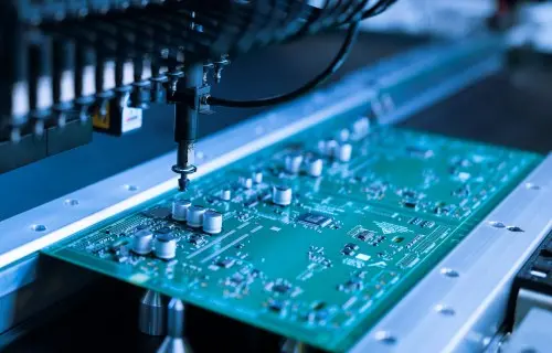
PCB assembly forms the foundation of most IoT devices, requiring precision component placement, soldering, and quality control processes. Following PCB completion, devices move through mechanical assembly stages where enclosures, connectors, displays, and other components are integrated to create functional products. Comprehensive testing protocols ensure devices meet performance specifications, regulatory requirements, and quality standards before final packaging and distribution.
The integration of these manufacturing stages requires sophisticated project management, supply chain coordination, and quality assurance systems. Successful manufacturers maintain flexibility to accommodate design changes while ensuring consistent production schedules and quality outcomes. Speed to market often determines competitive advantage in the rapidly evolving IoT landscape, making efficient manufacturing processes essential for success.
PCB Assembly: The Foundation of Smart Device Innovation
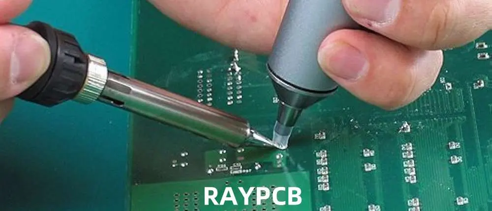
PCB assembly represents the critical foundation upon which all IoT devices are built, requiring precision, expertise, and advanced manufacturing capabilities. Modern PCB assembly processes must accommodate increasingly complex designs featuring high-density component placement, multi-layer boards, and components ranging from large power management ICs to microscopic passive components measuring just 0.4mm x 0.2mm.
Surface Mount Technology (SMT) dominates modern PCB assembly, enabling manufacturers to place components directly onto board surfaces using automated pick-and-place equipment. SMT processes support the miniaturization demands of IoT devices while maintaining high production speeds and consistent quality. Through-hole technology remains important for specific applications requiring robust mechanical connections, particularly for connectors, switches, and components subject to physical stress.
Quality control in PCB assembly involves multiple inspection stages, including automated optical inspection (AOI), in-circuit testing (ICT), and functional testing protocols. Advanced manufacturers utilize X-ray inspection for hidden solder joints and sophisticated testing equipment to verify electrical performance before components proceed to final assembly stages. The precision achieved in PCB assembly directly impacts device reliability, performance, and long-term durability.
Miniaturization trends in IoT device design place additional demands on PCB assembly capabilities. Manufacturers must maintain precise component placement tolerances while managing thermal considerations, signal integrity, and electromagnetic compatibility requirements. The expertise required for successful PCB assembly makes selecting the right manufacturing partner crucial for IoT device success.
Strategic Component Sourcing and Supply Chain Excellence
Effective component sourcing and supply chain management form the backbone of successful IoT & Smart Device Manufacturing operations. The global semiconductor shortage and supply chain disruptions of recent years have highlighted the critical importance of robust sourcing strategies and supplier relationships. Manufacturers must maintain visibility across complex supply networks while managing component availability, pricing fluctuations, and quality requirements.
IoT devices typically incorporate hundreds of components from dozens of suppliers, creating intricate supply chain dependencies that require careful management. Critical components like microcontrollers, sensors, and connectivity modules often have extended lead times and limited availability, necessitating strategic inventory planning and supplier diversification strategies. Forward-thinking manufacturers establish relationships with multiple suppliers for critical components while maintaining safety stock levels to prevent production delays.
Risk mitigation strategies include comprehensive supplier qualification processes, regular supply chain audits, and contingency planning for potential disruptions. Manufacturers must balance cost optimization with supply security, often maintaining premium supplier relationships for critical components while seeking cost advantages for commodity items. Real-time supply chain visibility tools enable proactive management of potential shortages and facilitate rapid response to changing market conditions.
The complexity of IoT component sourcing extends beyond traditional electronics to include specialized sensors, wireless modules, and application-specific integrated circuits. Successful manufacturers maintain deep technical knowledge of component specifications, alternative sourcing options, and emerging technologies that may impact future designs. This expertise enables them to provide valuable guidance to clients while ensuring reliable component availability throughout product lifecycles.
Design for Manufacturability: Optimizing Products for Production Success
Design for Manufacturability (DFM) principles play a crucial role in IoT & Smart Device Manufacturing, significantly impacting production costs, quality outcomes, and time-to-market performance. DFM involves optimizing product designs to facilitate efficient manufacturing processes while maintaining functionality and performance requirements. Early collaboration between design engineering and manufacturing teams prevents costly redesigns and production delays.
Effective DFM implementation considers component selection, PCB layout optimization, mechanical design constraints, and assembly process requirements. Designers must balance performance requirements with manufacturing practicalities, selecting components with reliable supply chains and proven manufacturing compatibility. PCB layouts should minimize component placement complexity while ensuring adequate spacing for automated assembly equipment and quality inspection processes.
Mechanical design aspects of DFM include enclosure design, fastener selection, and assembly sequence optimization. Simple, straightforward assembly processes reduce labor costs and minimize opportunities for errors while maintaining product quality and durability. Standardizing fasteners, minimizing unique components, and designing self-aligning features can significantly improve manufacturing efficiency and reduce production costs.
The collaborative approach to DFM extends beyond internal teams to include manufacturing partners who provide valuable insights based on production experience and equipment capabilities. This partnership approach enables designers to leverage manufacturing expertise while maintaining design integrity and performance requirements. Regular design reviews and prototype testing validate DFM decisions and identify opportunities for further optimization before committing to full-scale production.
From Assembly to Market-Ready Products
The transition from PCB assembly to finished goods represents a complex manufacturing phase requiring coordination of multiple processes, quality systems, and logistics operations. Following PCB completion and testing, devices move through mechanical assembly stages where enclosures, displays, connectors, and other components are integrated to create complete products. This phase requires careful attention to mechanical tolerances, assembly sequences, and quality control procedures.
Enclosure design and mechanical assembly significantly impact product functionality, durability, and user experience. Manufacturers must ensure proper fit and finish while maintaining ingress protection ratings, thermal management, and electromagnetic compatibility requirements. Software integration and configuration processes occur during this phase, requiring specialized equipment and procedures to load firmware, configure device settings, and verify functionality.
Comprehensive testing protocols validate complete product performance, regulatory compliance, and quality standards. Testing may include environmental stress testing, electromagnetic compatibility verification, wireless performance validation, and user acceptance testing. Products must meet various certification requirements including FCC, CE, and industry-specific standards before market release.
Final packaging, branding, and fulfillment logistics complete the manufacturing process, requiring coordination with marketing teams, distribution partners, and retail channels. Packaging design must protect products during shipping while supporting marketing objectives and regulatory labeling requirements. Efficient fulfillment systems enable rapid order processing and delivery to support launch schedules and ongoing sales operations.
Scalability and Customization in IoT Manufacturing
Modern IoT & Smart Device Manufacturing must accommodate diverse production requirements ranging from small prototype quantities to millions of units annually. This scalability challenge requires flexible manufacturing systems, modular production processes, and adaptive quality control procedures that maintain consistency across different production volumes. Successful manufacturers invest in scalable infrastructure and processes that can efficiently handle varying production demands.
Low-volume production scenarios often require more manual processes and flexible setup procedures, while high-volume manufacturing benefits from automated systems and optimized workflows. Manufacturers must balance investment in automation with the flexibility needed to accommodate diverse client requirements and changing market demands. Modular production approaches enable efficient scaling while maintaining quality standards and cost competitiveness.
Customization capabilities represent another critical differentiator in IoT manufacturing. Clients may require unique enclosure designs, specialized component configurations, or custom software implementations that differentiate their products in competitive markets. Manufacturers must maintain engineering expertise and flexible production systems to accommodate these customization requirements without compromising efficiency or quality.
The ability to support both startup companies and established enterprises requires different approaches to project management, quality assurance, and customer support. Startups often need extensive design support and rapid prototyping capabilities, while enterprise clients may require sophisticated supply chain integration and comprehensive quality documentation. Successful manufacturers develop service offerings tailored to these different client segments while maintaining operational efficiency.
Real-World Success Stories in IoT Manufacturing
Consider the case of a smart home security company that partnered with an experienced IoT manufacturer to bring their innovative wireless camera system to market. The project began with design optimization for manufacturability, reducing component count by 15% while improving reliability and reducing production costs. The manufacturer’s expertise in RF design and antenna integration resolved early connectivity issues and improved product performance.
The PCB assembly phase leveraged advanced SMT processes to accommodate the device’s compact form factor while maintaining high-density component placement. Specialized testing procedures validated wireless performance, power consumption, and environmental durability. The manufacturer’s supply chain expertise ensured component availability during the product launch period, preventing potential delays that could have impacted market entry timing.
From initial prototype to full production, the project timeline was compressed from 18 months to 12 months through efficient collaboration and parallel processing of design and manufacturing preparation activities. The final product achieved all performance targets while meeting aggressive cost requirements, enabling successful market launch and rapid sales growth.
Another example involves an industrial IoT sensor manufacturer that required ruggedized devices capable of operating in harsh environmental conditions. The manufacturing partner’s expertise in conformal coating, environmental testing, and quality assurance processes ensured products met stringent reliability requirements. Comprehensive testing protocols validated performance across temperature extremes, humidity variations, and vibration conditions typical of industrial applications.
These success stories demonstrate the value of experienced manufacturing partnerships in achieving project objectives while managing risks, costs, and timelines. The combination of technical expertise, manufacturing capabilities, and supply chain management creates significant competitive advantages for IoT product developers.
Selecting the Ideal Manufacturing Partner
Choosing the right manufacturing partner represents one of the most critical decisions in IoT product development, directly impacting product quality, time-to-market, and long-term success. Evaluation criteria should include technical capabilities, manufacturing experience, quality certifications, and financial stability. Partners should demonstrate expertise in IoT-specific requirements including wireless integration, sensor technologies, and connectivity protocols.
Manufacturing capabilities assessment should cover PCB assembly capabilities, mechanical assembly processes, testing equipment, and quality control systems. Partners should maintain modern equipment, appropriate certifications (ISO 9001, ISO 13485, etc.), and documented quality management systems. Experience with similar products or technologies provides valuable insights and reduces project risks.
End-to-end service capabilities distinguish exceptional manufacturing partners from basic contract manufacturers. Services should include design support, prototyping, supply chain management, quality assurance, and fulfillment logistics. This comprehensive approach simplifies project management while ensuring consistency across all manufacturing phases.
Cost considerations must balance price competitiveness with value-added services and quality outcomes. While initial pricing may seem attractive, total cost of ownership includes quality issues, delivery delays, and ongoing support requirements. Successful partnerships focus on long-term value creation rather than short-term cost minimization.
Communication capabilities and project management expertise are often overlooked but critically important factors. Partners should provide regular updates, proactive issue identification, and responsive customer support throughout the manufacturing process. Clear communication protocols and dedicated project management resources ensure smooth project execution and client satisfaction.
Conclusion and Next Steps
The IoT & Smart Device Manufacturing landscape continues evolving rapidly, driven by technological advancement, market demand, and competitive pressures. Success in this dynamic environment requires manufacturing partners who combine technical expertise, operational excellence, and strategic thinking to deliver innovative products efficiently and cost-effectively.
From initial PCB assembly through final product delivery, every manufacturing phase contributes to overall product success. The integration of design optimization, supply chain management, quality assurance, and logistics coordination creates competitive advantages that enable successful product launches and sustained market growth. Companies that invest in experienced manufacturing partnerships position themselves for long-term success in the expanding IoT marketplace.
The complexity of modern IoT devices demands manufacturing partners who understand both technical requirements and market dynamics. By selecting partners with comprehensive capabilities, proven experience, and commitment to quality, product developers can focus on innovation while ensuring manufacturing excellence supports their business objectives.
Ready to transform your IoT concept into a market-ready product? Contact our experienced manufacturing team to discuss your project requirements and discover how our comprehensive services can accelerate your path to market success.
Frequently Asked Questions
Q: What is the typical timeline for IoT device manufacturing from PCB assembly to finished goods?
A: The timeline varies significantly depending on product complexity, testing requirements, and production volume. Simple IoT devices may complete the journey in 6-8 weeks, while complex products requiring extensive testing and certification can take 12-16 weeks or longer. Factors affecting timeline include component availability, tooling requirements, software integration complexity, and regulatory certification needs.
Q: How do you ensure quality control throughout the IoT manufacturing process?
A: Quality control involves multiple inspection stages including incoming component inspection, in-process testing during PCB assembly, functional testing of completed assemblies, and final product validation. We utilize automated optical inspection (AOI), in-circuit testing (ICT), and comprehensive functional testing protocols. All processes follow ISO 9001 quality management systems with documented procedures and traceability records.
Q: What are the minimum order quantities for IoT device manufacturing?
A: Minimum order quantities depend on product complexity and manufacturing requirements. For prototype and low-volume production, quantities as low as 10-50 units may be feasible. Standard production runs typically start at 500-1000 units for cost-effective manufacturing. High-volume production offers the best cost efficiency but requires quantities of 10,000 units or more.
Q: How do you handle component shortages and supply chain disruptions?
A: We maintain strategic supplier relationships, safety stock levels, and alternative sourcing options for critical components. Our supply chain management team monitors component availability and provides early warnings of potential shortages. We work closely with clients to identify alternative components when necessary and maintain flexibility in production scheduling to accommodate supply chain variations.
Q: What certifications and regulatory compliance do you support for IoT devices?
A: We support comprehensive certification requirements including FCC (United States), CE (European Union), IC (Canada), and various industry-specific standards. Our testing capabilities include electromagnetic compatibility (EMC), wireless performance, safety standards, and environmental compliance. We maintain relationships with accredited testing laboratories and can coordinate certification processes to ensure regulatory compliance in target markets.
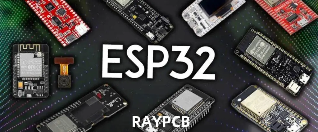
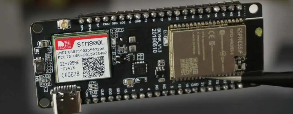
Welcome to the world of ESP32! If you’re stepping into the exciting realm of Internet of Things (IoT) and embedded systems, you’ve come to the right place. This comprehensive guide will walk you through everything you need to know about the ESP32, from its basic features to programming tips and beginner-friendly projects.
What is the ESP32?
The ESP32 is a powerful, low-cost microcontroller that has taken the maker community by storm. It’s the successor to the popular ESP8266 and packs a punch with its dual-core processor, built-in Wi-Fi and Bluetooth capabilities, and extensive GPIO options. Whether you’re building a smart home device, a wearable gadget, or an industrial sensor network, the ESP32 provides a versatile platform for your projects.
Why is it so popular for IoT and embedded projects?
The ESP32’s popularity stems from its perfect balance of features, cost, and ease of use. Here’s why makers and professionals alike love it:
Powerful processing: Dual-core processor up to 240MHz
Low power consumption: Ideal for battery-operated devices
Rich peripherals: ADC, DAC, touch sensors, and more
Affordable: High-end features at a budget-friendly price
Strong community support: Abundant resources and libraries
What this guide covers
In this guide, we’ll dive deep into the ESP32, covering everything from basic setup to advanced programming tips. You’ll learn about the ESP32’s pinout, how to set up your development environment, and how to bring your ideas to life with practical projects. Whether you’re a complete beginner or looking to expand your ESP32 skills, this guide has something for everyone.
Let’s embark on this exciting journey into the world of ESP32!
The ESP32 is the successor to the widely popular ESP8266, both developed by Espressif Systems. While the ESP8266 revolutionized the IoT landscape with its low-cost Wi-Fi capabilities, the ESP32 takes it a step further by addressing many of its predecessor’s limitations and adding new features.
Introduced in 2016, the ESP32 quickly gained traction in the maker community and professional circles alike. Its combination of powerful processing, wireless connectivity, and affordability made it an instant hit for a wide range of applications.
Key Features
The ESP32 boasts an impressive array of features that set it apart:
Dual-core processor: Two Xtensa 32-bit LX6 microprocessors that can be controlled separately
Clock speed: Up to 240 MHz
Wi-Fi: 2.4 GHz Wi-Fi (802.11 b/g/n)
Bluetooth: Bluetooth v4.2 BR/EDR and BLE (Bluetooth Low Energy)
Low power modes: Deep sleep mode consuming only 10µA
Popular Variants
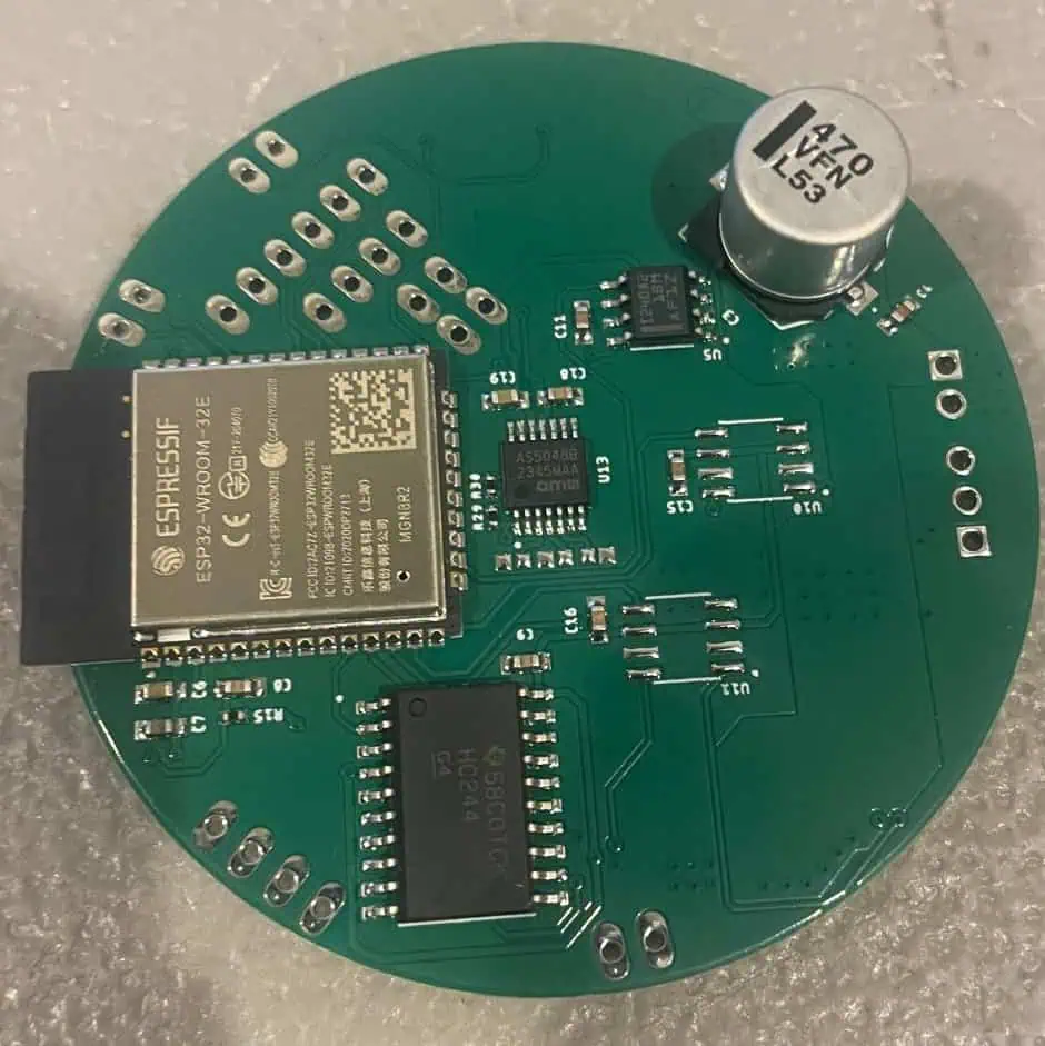
The ESP32 comes in several variants to suit different project needs:
ESP32-WROOM: The most common module, featuring Wi-Fi and Bluetooth
ESP32-WROVER: Similar to WROOM but with additional PSRAM
ESP32-CAM: Includes a camera module, perfect for video streaming projects
ESP32-S2: A single-core variant with enhanced security features
ESP32-C3: RISC-V based variant with Wi-Fi and Bluetooth LE
Each variant has its strengths, making the ESP32 family versatile enough to cater to a wide range of project requirements.
ESP32 Pinout Overview
Understanding the ESP32’s pinout is crucial for connecting sensors, actuators, and other components to your projects. Let’s break down the most important pins and their functions.
Standard Pinout Diagram
[Insert image of ESP32 pinout diagram here]
Important Pins Explained
Power Pins
3V3: 3.3V power output
GND: Ground
VIN: Input voltage (5V typically)
GPIO (General Purpose Input/Output)
The ESP32 has up to 36 GPIO pins, but not all are available on every module. Some key points:
GPIO 0-39 are available (with some exceptions)
Some pins have special functions (e.g., GPIO 0 is used for booting)
GPIO 6-11 are typically used for connecting the onboard flash, avoid using these
Be aware of the default boot states of pins to prevent unintended behavior
Understanding these pin functions and limitations will help you design your projects more effectively and avoid common pitfalls when working with the ESP32.
Setting Up Your ESP32 for the First Time
Getting started with the ESP32 is straightforward, but there are a few key steps to follow. Let’s walk through the process of setting up your development environment.
What You Need
ESP32 development board (e.g., ESP32-WROOM or ESP32-DevKitC)
void setup() { Serial.begin(115200); WiFi.begin(ssid, password); while (WiFi.status() != WL_CONNECTED) { delay(1000); Serial.println("Connecting to WiFi..."); } Serial.println("Connected to WiFi"); Serial.print("IP address: "); Serial.println(WiFi.localIP());
server.on("/", handleRoot); server.begin(); Serial.println("HTTP server started"); }
void loop() { server.handleClient(); }
void handleRoot() { String html = "<html><body><h1>ESP32 Web Server</h1><p>Hello from ESP32!</p></body></html>"; server.send(200, "text/html", html); }
3. Basic Bluetooth Communication
Implement a simple Bluetooth Low Energy (BLE) server:
pCharacteristic->setValue("Hello World"); pService->start(); BLEAdvertising *pAdvertising = BLEDevice::getAdvertising(); pAdvertising->addServiceUUID(SERVICE_UUID); pAdvertising->setScanResponse(true); pAdvertising->setMinPreferred(0x06); // functions that help with iPhone connections issue pAdvertising->setMinPreferred(0x12); BLEDevice::startAdvertising(); Serial.println("Characteristic defined! Now you can read it in your phone!"); }
These projects provide a solid foundation for understanding key ESP32 features. As you become more comfortable, you can combine these concepts to create more complex and interesting applications
Programming Tips and Best Practices
ESP32 Programming Circuit
To make the most of your ESP32 projects, consider these programming tips and best practices:
Using Deep Sleep to Save Power
The ESP32’s deep sleep mode is crucial for battery-operated projects. Here’s how to implement it:
#define uS_TO_S_FACTOR 1000000 // Conversion factor for micro seconds to seconds #define TIME_TO_SLEEP 5 // Time ESP32 will go to sleep (in seconds)
void loop() { if (WiFi.status() != WL_CONNECTED) { Serial.println("Reconnecting to WiFi..."); WiFi.disconnect(); WiFi.reconnect(); delay(5000); } // Your main code here }
OTA (Over-the-Air) Updates Basics
OTA updates allow you to upload new code to your ESP32 wirelessly:
The ESP32 is a powerful and versatile microcontroller that opens up a world of possibilities for IoT and embedded projects. This guide has covered the basics of getting started with the ESP32, from understanding its pinout to programming your first projects.
We encourage you to try out the projects we’ve discussed and experiment with your own ideas. The ESP32’s flexibility makes it an excellent platform for learning and innovation. As you grow more comfortable with the basics, you can explore more advanced topics like:
Using FreeRTOS for multitasking
Implementing Micropython on ESP32
Creating mesh networks with ESP-NOW
Integrating ESP32 with cloud platforms like AWS IoT or Google Cloud IoT
Remember, the best way to learn is by doing. Start small, build on your successes, and don’t be afraid to ask for help in the ESP32 community. Happy coding!
FAQ: Quick Answers for ESP32 Beginners
Q: Can ESP32 run on 5V? A: While the ESP32 chip operates at 3.3V, many development boards have a voltage regulator that allows you to power them with 5V via USB or VIN pin.
Q: How much memory does ESP32 have? A: The typical ESP32 has 520 KB of SRAM and 448 KB of ROM. Some variants may have different amounts.
Q: Can ESP32 connect to 5GHz Wi-Fi? A: No, the standard ESP32 only supports 2.4GHz Wi-Fi. Some newer variants like the ESP32-C6 support 5GHz.
Q: How many GPIO pins does ESP32 have? A: The ESP32 chip has up to 36 GPIO pins, but the number available on development boards may vary.
Q: Can ESP32 run Arduino code? A: Yes, the ESP32 can be programmed using the Arduino IDE and most Arduino libraries.
While the ESP8266 is still a capable and cost-effective option for simpler projects, the ESP32’s additional features and processing power make it the better choice for more complex applications, especially those requiring Bluetooth or advanced GPIO functionality.
In the ever-evolving landscape of modern electronics, integrated circuits (ICs) stand as the cornerstone of technological progress. These miniature marvels, often no larger than a fingernail, are the brains behind our smartphones, computers, and countless other devices that power our digital world. At the heart of bringing these complex components to life lies the crucial process of integrated circuit assembly.
Integrated circuit assembly is the intricate art and science of transforming raw semiconductor materials into functional electronic components. This process involves a series of precise steps, each critical to ensuring the performance, reliability, and longevity of the final product. As technology continues to advance at a breakneck pace, the techniques and innovations in IC assembly play an increasingly vital role in shaping the future of electronics.
This article aims to explore the key techniques, recent innovations, and future trends in integrated circuit assembly. By delving into both traditional methods and cutting-edge advancements, we’ll uncover how this field is pushing the boundaries of what’s possible in electronic design and manufacturing.
Integrated circuit assembly refers to the process of packaging a semiconductor die (chip) into a functional IC package. This process transforms a bare silicon chip into a protected, usable component that can be integrated into electronic devices. The scope of IC assembly encompasses everything from preparing the die to final testing of the packaged chip.
Overview of Assembly Stages
The integrated circuit assembly process can be broadly divided into four main stages:
Die Preparation: This involves separating individual dies from the processed wafer and preparing them for packaging.
Bonding: The die is attached to the package substrate and electrical connections are made between the die and the package leads.
Packaging: The assembled die is encapsulated in a protective material to shield it from environmental factors and physical damage.
Testing: The packaged IC undergoes rigorous testing to ensure functionality and reliability.
Key Materials Used in IC Assembly
Several crucial materials are employed throughout the IC assembly process:
Substrates: Typically made of materials like ceramic, plastic, or glass, these serve as the base for the IC package.
Adhesives: Used to attach the die to the substrate.
Bonding wires: Usually gold or copper, these create electrical connections between the die and package leads.
Encapsulants: Protective materials that surround the die and internal connections.
Solder: Used for creating external connections on the package.
Traditional Techniques in IC Assembly
Wire Bonding
Wire bonding is one of the most widely used techniques in IC assembly. It involves creating electrical connections between the die and the package leads using thin wires, typically made of gold or copper.
Types of Wire Bonding
Ball bonding
Wedge bonding
Advantages
Flexible and adaptable to different package types
Well-established technology with high reliability
Cost-effective for many applications
Flip-Chip Bonding
Flip-chip bonding, also known as controlled collapse chip connection (C4), involves flipping the chip upside down and directly connecting it to the substrate using solder bumps.
Key Features
Direct die-to-substrate connection
Higher performance due to shorter electrical paths
Wafer-level packaging (WLP) is a technique where the IC packaging is done at the wafer level, before the individual chips are separated.
Benefits
Smaller package size, approaching chip scale
Improved electrical performance
Cost-effective for high-volume production
Limitations of Conventional Approaches
While these traditional techniques have served the industry well, they face limitations in meeting the demands of modern electronics:
Challenges in achieving extremely fine pitches
Thermal management issues in high-performance applications
Difficulties in integrating heterogeneous components
Innovations and Emerging Techniques
As the electronics industry pushes for smaller, faster, and more powerful devices, new techniques in integrated circuit assembly have emerged to meet these challenges.
3D Integrated Circuits (3D ICs)
3D ICs represent a significant leap forward in IC assembly, allowing for vertical stacking of multiple dies.
Through-Silicon Vias (TSVs)
TSVs are a key enabling technology for 3D ICs. These are vertical electrical connections that pass through a silicon wafer or die, allowing for direct connections between stacked layers.
Benefits for Performance and Miniaturization
Reduced signal delay and power consumption
Higher bandwidth between different functional blocks
Significant reduction in overall package size
System-in-Package (SiP) Technology
SiP technology takes integration a step further by combining multiple ICs and other components into a single package.
Integration of Heterogeneous Components
SiP allows for the integration of different types of chips and components, such as:
This level of integration enables more compact and powerful electronic systems, crucial for applications like smartphones and IoT devices.
Fan-Out Wafer-Level Packaging (FOWLP)
FOWLP is an advanced wafer-level packaging technique that extends the benefits of WLP to chips with a higher number of I/O connections.
Improved Thermal and Electrical Performance
Better heat dissipation due to larger package area
Shorter electrical paths leading to improved signal integrity
Ability to integrate more I/Os in a smaller form factor
Advanced Materials and Processes
The quest for improved performance has led to the development and adoption of new materials and processes in IC assembly.
Use of Low-k Dielectrics
Low-k dielectric materials are being increasingly used to reduce signal delay and power consumption in high-performance ICs.
New Solder Materials
Lead-free solder alloys and copper pillar bumps are being adopted to meet environmental regulations and improve electrical and thermal performance.
AI-based Inspection Tools
Artificial intelligence and machine learning are being employed in inspection and quality control processes, improving defect detection and yield rates.
The aerospace and defense sectors leverage cutting-edge IC assembly for:
High-reliability avionics systems
Advanced radar and communication equipment
Radiation-hardened components for space applications
Conclusion
The field of integrated circuit assembly stands at the forefront of technological innovation, continuously pushing the boundaries of what’s possible in electronic design and manufacturing. From traditional wire bonding techniques to cutting-edge 3D IC technologies, the evolution of IC assembly has been nothing short of remarkable.
As we’ve explored in this article, recent innovations like 3D ICs, advanced packaging techniques, and smart manufacturing processes are reshaping the landscape of electronics manufacturing. These advancements are not only meeting the demands for smaller, faster, and more powerful devices but also addressing critical challenges in thermal management, cost reduction, and environmental sustainability.
Looking ahead, the role of integrated circuit assembly in next-generation electronics is set to become even more crucial. As we venture into the realms of quantum computing, neuromorphic systems, and beyond, IC assembly techniques will need to evolve to meet these new challenges. The integration of AI, advanced materials, and sustainable practices will undoubtedly play a significant role in shaping the future of this field.
The journey of innovation in IC assembly is far from over. It calls for continued research, industry collaboration, and a relentless pursuit of technological excellence. As we stand on the brink of new frontiers in electronics, the advancements in integrated circuit assembly will continue to be a driving force, enabling the technologies that will define our future.
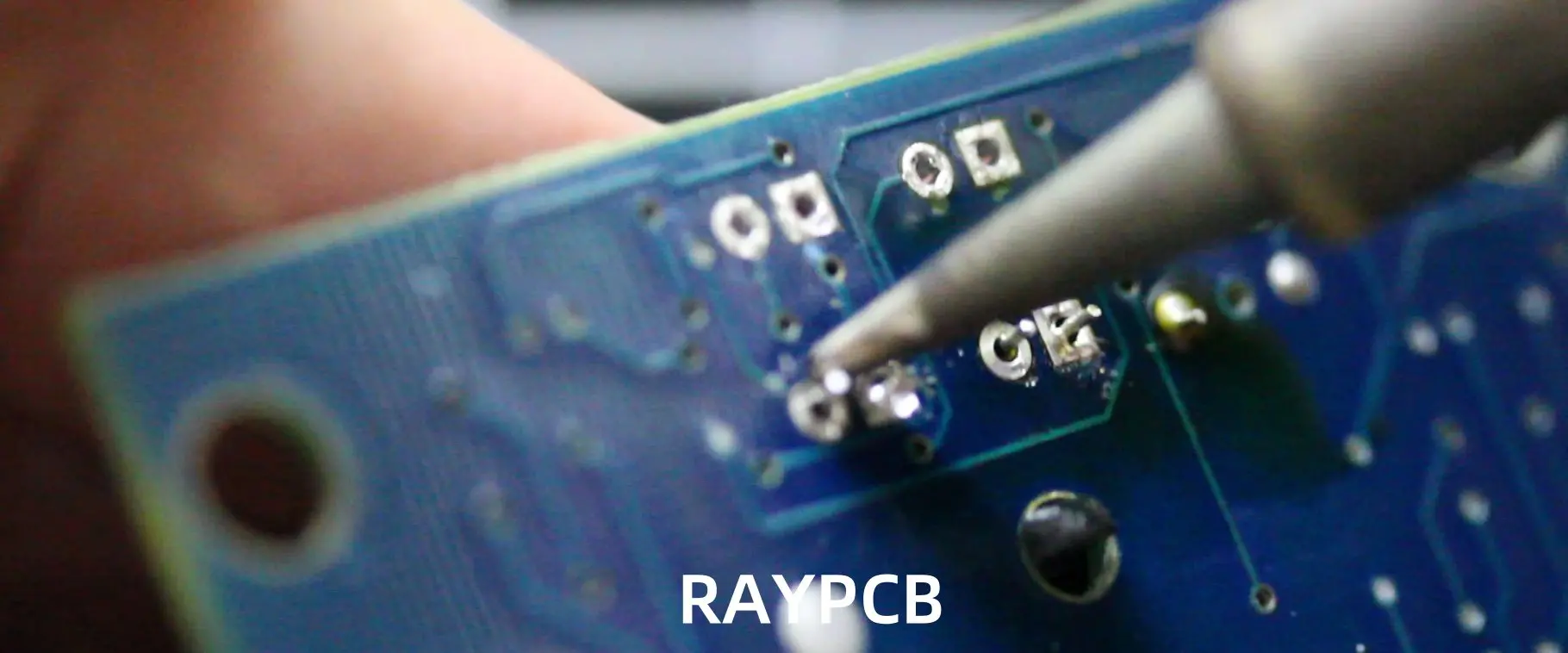
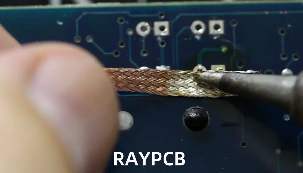
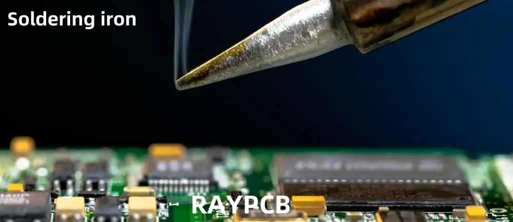
In the world of electronics repair and modification, knowing how to remove solder from a Printed Circuit Board (PCB) is an essential skill. Whether you’re replacing a faulty component, modifying a circuit, or salvaging parts, mastering the art of desoldering can save you time, money, and frustration.
Why Removing Solder Matters
Removing solder from a PCB is crucial for several reasons:
Component replacement: When a component fails, it needs to be removed and replaced.
Circuit modification: Desoldering allows for circuit modifications and upgrades.
PCB repair: Removing solder is often the first step in repairing damaged traces or pads.
Parts salvage: Desoldering lets you recover valuable components from old or discarded boards.
Challenges in Removing Solder
Desoldering isn’t always straightforward. Some common challenges include:
Risk of damaging the PCB or nearby components
Dealing with lead-free solder, which has a higher melting point
Removing solder from multi-layer boards or plated through-holes
Working with small or densely packed components
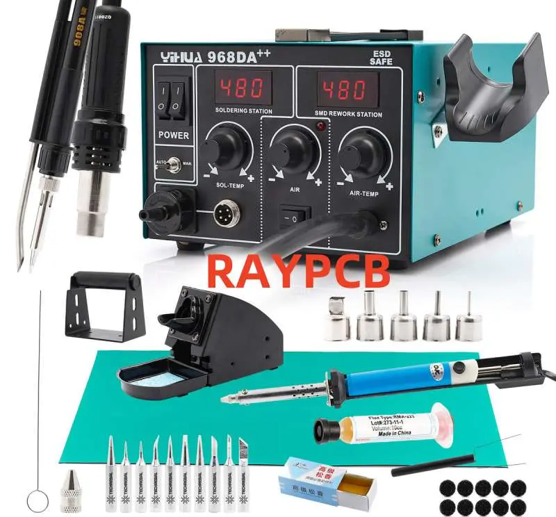
Tools Preview
Before diving into the methods, let’s preview the essential tools for removing solder:
For more complex desoldering tasks, advanced techniques and tools may be necessary.
1 Hot Air Rework Station
Hot air rework stations are ideal for removing surface-mount components with multiple pins.
Process:
Apply flux to all pins of the component.
Set the hot air temperature (typically 315-370°C or 600-700°F) and airflow.
Move the hot air nozzle in a circular motion over the component.
Once all solder joints are molten, carefully remove the component with tweezers.
Advantages:
Reduces the risk of pad damage compared to individual pin desoldering.
Ideal for BGA (Ball Grid Array) and QFP (Quad Flat Package) components.
2 Low-Temp Solder Alloy
Low-temperature solder alloys can be used to remove components with less heat exposure.
Process:
Apply low-temp solder to all joints of the component.
Heat the joints until all solder is molten.
Remove the component while the solder is liquid.
Benefits:
Reduces the risk of thermal damage to sensitive components.
Useful for working with heat-sensitive parts or multi-layer PCBs.
3 Manual Tools
For certain applications, specialized manual tools can be effective:
Desoldering tweezers: Heated tweezers that melt solder on both sides of a component simultaneously.
Spring-loaded desoldering irons: Combine a soldering iron with a built-in suction mechanism.
Special Cases & Troubleshooting
1 Removing Solder from Holes
Plated through-holes can be particularly challenging to desolder.
Technique:
Use a solder sucker in combination with a soldering iron.
If unsuccessful, try adding fresh solder to improve heat transfer.
For stubborn holes, use a desoldering braid from both sides of the board.
2 Dealing with Stubborn Residue
Sometimes, a thin layer of solder remains after desoldering.
Solutions:
Use flux and a fine-tipped soldering iron to re-melt and remove the residue.
Try a fiberglass brush pen to gently scrub away remaining solder.
3 Removing Solder Without an Iron
In emergencies, solder can be removed without specialized tools:
Methods:
Use a lighter to heat the solder and quickly tap the board to shake off molten solder.
For through-hole components, heat the solder and use a paperclip or pin to push through the hole.
Caution: These methods carry a high risk of board damage and should only be used as a last resort.
Post-Desoldering Cleanup
Proper cleanup after desoldering is crucial for the longevity and reliability of your PCB.
1 Removing Flux Residue
Flux residue can cause corrosion and affect the board’s performance if left uncleaned.
Cleaning methods:
For rosin-based flux: Use isopropyl alcohol and a soft brush.
For no-clean flux: Often doesn’t require cleaning, but can be removed with specialized solvents if necessary.
For water-soluble flux: Clean with warm water and a soft brush, then dry thoroughly.
2 Inspection
After cleaning, inspect the board thoroughly:
Check for any remaining solder bridges or residue.
Examine pads and traces for signs of damage or lifting.
Use a magnifying glass or microscope for detailed inspection of small components.
3 Preventing Oxidation
Exposed copper can quickly oxidize, making future soldering difficult.
Protection methods:
Apply a thin layer of solder (tinning) to exposed pads.
Use a PCB lacquer spray to protect the entire board if it won’t be immediately reused.
Frequently Asked Questions
1 Can solder be completely removed from a PCB?
While it’s challenging to remove 100% of the solder, with proper techniques and tools, you can remove enough solder for successful component replacement or board modification.
2 How can I remove solder without a wick or pump?
In a pinch, you can use aluminum foil as a makeshift wick. Place a small strip of foil on the joint, apply the soldering iron, and the foil will absorb the molten solder.
3 How do I remove solder from speaker terminals or through-hole pins?
For large terminals or pins, heat the solder and use pliers to gently wiggle and pull the component while the solder is molten. Be careful not to apply too much force, which could damage the board.
Safety & Best Practices
1 Ventilation
Always work in a well-ventilated area to avoid inhaling solder fumes.
Use a fume extractor if working indoors.
Consider wearing a mask designed for soldering work.
Use an ESD-safe workstation with a grounded mat and wrist strap.
Handle components and boards by their edges to minimize static risk.
3 Temperature Control
Proper temperature control is crucial for effective desoldering and component protection.
Start with lower temperatures and increase as needed.
Allow components and the board to cool between desoldering attempts.
Use heat sinks on nearby components to prevent collateral heat damage.
Conclusion
Mastering the art of removing solder from PCBs is a valuable skill in electronics repair and modification. By understanding the various tools and techniques available, you can tackle a wide range of desoldering challenges safely and effectively.
Remember that practice makes perfect. Start with simpler projects and work your way up to more complex boards. Always prioritize safety, use the right tools for the job, and take your time to avoid damaging valuable components or PCBs.
Whether you’re a hobbyist tinkering with electronics or a professional repairing high-end equipment, the ability to cleanly and efficiently remove solder will serve you well in your electronic endeavors. Happy desoldering!
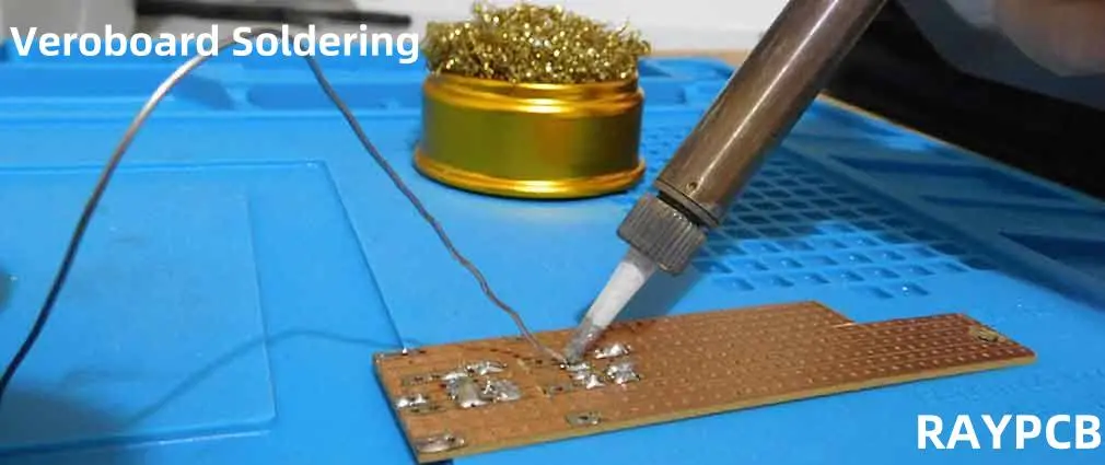
Veroboard soldering is an essential skill for electronics enthusiasts and professionals alike. This versatile prototyping method allows you to create custom circuits quickly and efficiently. In this comprehensive guide, we’ll explore everything you need to know about Veroboard soldering, from the basics to advanced techniques.
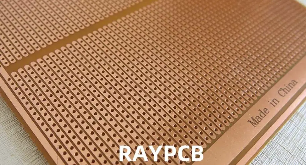
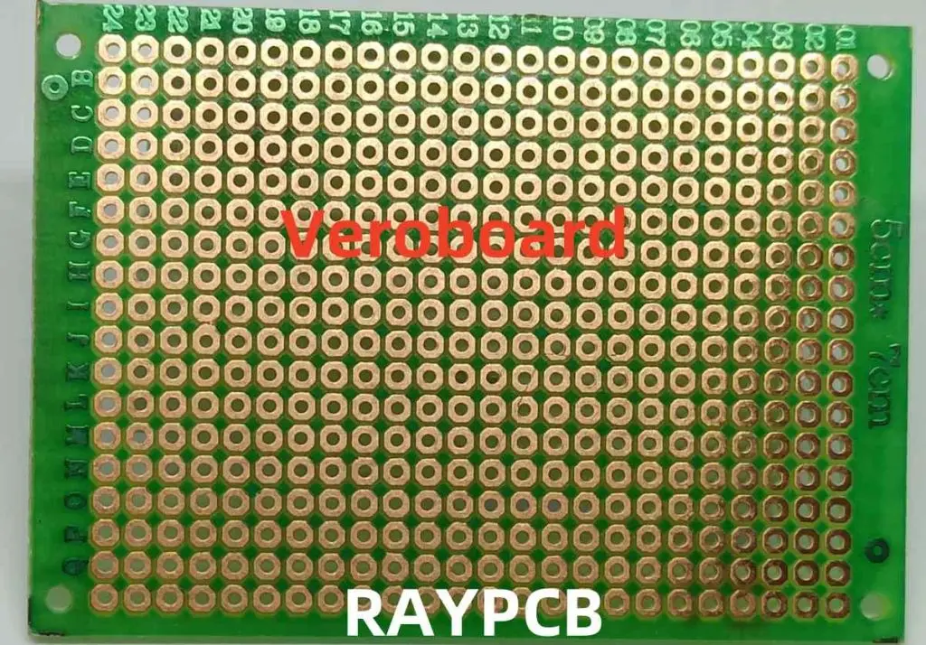
What is Veroboard?
Veroboard, also known as stripboard, is a type of prototyping board with copper strips and pre-drilled holes. It’s an excellent alternative to custom-printed circuit boards (PCBs) for small-scale projects and prototypes.
Essential Tools for Veroboard Soldering
Before diving into the soldering process, let’s review the tools you’ll need for successful Veroboard soldering:
Mixed-Technology Boards: Combine through-hole and surface-mount components
Multi-Layer Designs: Stack Veroboards for complex 3D circuits
Custom Enclosures: Design and build enclosures around your Veroboard circuits
Future Trends in Prototyping and Veroboard Alternatives
While Veroboard remains popular, new prototyping methods are emerging:
3D-Printed Circuit Boards: Rapid prototyping with conductive filaments
Flexible PCBs: Adaptable circuits for wearable technology
Paper Electronics: Low-cost, disposable circuit prototyping
Modular Prototyping Systems: Pre-made circuit blocks for quick assembly
Conclusion: Mastering Veroboard Soldering
Veroboard soldering is a valuable skill that bridges the gap between breadboard prototypes and custom PCBs. With practice and patience, you can create professional-quality circuits for a wide range of applications. Remember these key points:
Proper preparation is crucial for successful Veroboard projects
Technique matters: focus on creating clean, strong solder joints
Start with simple projects and gradually increase complexity
Always prioritize safety in your workspace
Maintain your tools for consistent performance
Whether you’re a hobbyist or a professional, mastering Veroboard soldering will expand your capabilities in circuit design and prototyping. Keep practicing, stay curious, and don’t be afraid to tackle challenging projects. With time, you’ll be soldering Veroboard circuits like a pro!
Soldering is an essential skill in electronics repair, especially when replacing faulty components on a PCB. But before you can solder a new part in place, you must first remove the old one—making desoldering the critical first step. For most hobbyists and makers, the go-to tool for this job is the humble solder sucker (also known as a desoldering pump), offering a simple yet effective way to clear solder from joints.
Understanding Solder Removal Tools
Before we dive into the comparison, let’s briefly define our two contenders:
What is a Solder Sucker?
A solder sucker, also known as a desoldering pump, is a manual tool used to remove molten solder from a soldered joint. It works by creating a vacuum that sucks up the liquefied solder.
What is a Desoldering Gun?
A desoldering gun is an electrical tool that combines heat to melt the solder and suction to remove it, all in one device. It’s often more powerful and efficient than a manual solder sucker.
Solder Suckers: In-Depth Look
Let’s start by examining solder suckers in detail.
How Solder Suckers Work
Preparation: The spring-loaded piston is compressed and locked in place.
Heating: The solder joint is heated with a separate soldering iron.
Activation: The release button is pressed, creating a strong vacuum.
Suction: The molten solder is quickly drawn into the cylinder.
All-in-One: Combines heating and suction in one tool
Consistent Heat: Often features temperature control
Ergonomics: Designed for prolonged use with less fatigue
Precision: Some models offer fine temperature and suction control
Cons of Using a Desoldering Gun
Cost: Significantly more expensive than solder suckers
Power Requirement: Needs an electrical outlet to operate
Learning Curve: Can be more complex to use effectively
Maintenance: Requires regular cleaning and filter changes
Size and Weight: Generally bulkier and heavier than solder suckers
Comparing Solder Suckers and Desoldering Guns
Now that we’ve examined each tool individually, let’s compare them across various factors to help you decide which is right for your project.
1. Cost Comparison
Solder Suckers:
Entry-level: 5−5−20
Professional-grade: 20−20−50
Desoldering Guns:
Entry-level: 50−50−100
Professional-grade: 100−100−500+
Winner: Solder suckers are significantly more affordable, making them ideal for hobbyists and occasional users.
2. Ease of Use
Solder Suckers:
Simple operation
Requires coordination with a separate soldering iron
Minimal setup time
Desoldering Guns:
All-in-one operation
May have a steeper learning curve
Requires setup and warm-up time
Winner: Solder suckers are simpler to use, especially for beginners, but desoldering guns offer more convenience once mastered.
3. Efficiency and Speed
Solder Suckers:
Slower for large jobs
Requires frequent emptying
Manual operation can be tiring
Desoldering Guns:
Faster for extensive desoldering work
Continuous operation possible
Less physical effort required
Winner: Desoldering guns are more efficient, especially for larger projects or professional use.
4. Precision and Control
Solder Suckers:
Good for targeted, small-scale work
Precision depends on user skill
Limited control over suction strength
Desoldering Guns:
Adjustable temperature and suction on some models
Consistent heat application
Can be overkill for simple tasks
Winner: Tie. Solder suckers offer good precision for small tasks, while desoldering guns provide better control for complex work.
5. Portability
Solder Suckers:
Highly portable
No power source required
Lightweight and compact
Desoldering Guns:
Less portable due to power requirements
Heavier and bulkier
Some cordless models available, but limited
Winner: Solder suckers are much more portable, making them ideal for field work or tight spaces.
6. Maintenance
Solder Suckers:
Easy to disassemble and clean
Few or no consumable parts
Simple repairs possible
Desoldering Guns:
Regular cleaning required
Filter and nozzle replacements needed
More complex repairs, often requiring professional service
Winner: Solder suckers are easier and cheaper to maintain.
Choosing the Right Tool for Your Project
Now that we’ve compared solder suckers and desoldering guns, let’s look at which tool might be best for different types of projects and users.
For Hobbyists and Occasional Users
Recommended Tool: Solder Sucker
Reasons:
More affordable
Easier to learn and use
Sufficient for most small-scale projects
Low maintenance requirements
Best Practices:
Invest in a quality solder sucker for better results
Practice coordinating with your soldering iron
Keep the tip clean for optimal performance
For Professional Technicians and Frequent Users
Recommended Tool: Desoldering Gun
Reasons:
More efficient for large-scale work
Reduces hand fatigue during extended use
Provides consistent heat and suction
Often offers better precision for complex boards
Best Practices:
Choose a model with adjustable temperature and suction
Regularly clean and maintain your desoldering gun
Keep spare filters and nozzles on hand
For Mixed Use or Growing Hobbyists
Recommended Tool: Both
Reasons:
Solder sucker for simple tasks and portability
Desoldering gun for larger projects and efficiency
Best Practices:
Start with a quality solder sucker
Upgrade to a desoldering gun as skills and projects advance
Use each tool for its strengths
Tips for Effective Solder Removal
Regardless of which tool you choose, these tips will help you achieve better results:
Use Flux: Apply flux to improve heat transfer and solder flow
Add Fresh Solder: Sometimes adding a bit of fresh solder helps remove old, oxidized solder
Proper Heat: Ensure the solder is fully melted before attempting removal
Clean Tools: Regularly clean your solder sucker or desoldering gun for optimal performance
Practice: Start with scrap boards to improve your technique
Safety First: Always wear safety glasses and work in a well-ventilated area
Environmental and Safety Considerations
When working with solder removal tools, keep these environmental and safety factors in mind:
Environmental Impact
Proper disposal of removed solder (may contain lead)
Energy consumption of electric desoldering guns
Longevity and repairability of tools
Safety Precautions
Use in well-ventilated areas to avoid inhaling fumes
Wear safety glasses to protect against solder splatter
Be cautious of hot surfaces and components
Follow proper electrical safety with desoldering guns
Future Trends in Solder Removal Technology
As we look to the future, several trends are shaping the world of solder removal:
Increased Automation: Robotic desoldering for large-scale operations
Eco-Friendly Solutions: Development of lead-free solder removal techniques
Smart Tools: Integration of IoT and data logging in professional-grade tools
Improved Ergonomics: Focus on reducing user fatigue in both manual and electric tools
Hybrid Tools: Combination of different technologies for more versatile solder removal
Conclusion: Making Your Choice
Choosing between a solder sucker and a desoldering gun ultimately depends on your specific needs, budget, and the types of projects you undertake. Here’s a quick summary to help you decide:
Choose a Solder Sucker if:
You’re a hobbyist or occasional user
You’re on a tight budget
You need a portable solution
Your projects involve simple, small-scale desoldering
Choose a Desoldering Gun if:
You frequently work on large desoldering projects
You’re a professional or serious hobbyist
Efficiency and reduced fatigue are priorities
You’re willing to invest in a more powerful tool
Remember, many experienced electronics enthusiasts and professionals keep both tools in their arsenal, using each for its strengths. As you grow in your electronics journey, you may find that having both a reliable solder sucker and a efficient desoldering gun gives you the flexibility to tackle any project that comes your way.
Whichever tool you choose, practice and patience will help you master the art of solder removal, leading to cleaner, more professional results in all your electronics projects.
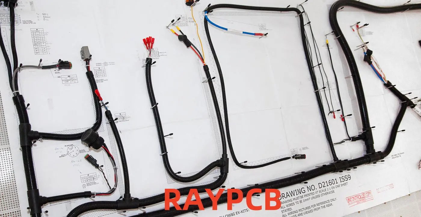
A wire harness (also called a cable harness or wiring assembly) is an organized arrangement of wires, cables, and subassemblies designed to transmit electrical power or signals efficiently. While a simple harness may consist of just a few components, more complex versions can incorporate dozens—or even hundreds—of wires, connectors, and passive (or active) elements.
In today’s interconnected world, the importance of efficient and reliable electrical systems cannot be overstated. At the heart of these systems lies a crucial component: the wire harness assembly. Whether you’re in the automotive industry, aerospace, or consumer electronics, understanding wire harness assemblies is essential for creating robust and efficient electrical systems. This comprehensive guide will delve into the world of wire harness assemblies, exploring their types, benefits, design processes, and manufacturing
techniques.
What is Wire Harness Assembly?
Wire harness assembly is the process of organizing and bundling individual electrical wires or cables into a single unit. This unified structure, known as a wire harness or wiring assembly, serves as the central nervous system for various electrical devices and systems. By consolidating multiple wires into a single harness, manufacturers can streamline installation, improve organization, and enhance the overall reliability of electrical systems.
Key Components of a Wire Harness
Wires and cables
Connectors
Terminals
Sleeves and sheaths
Clips and fasteners
Labels and identifiers
Wire harness assemblies play a crucial role in transmitting power, data, and signals between different components of a system. They are designed to withstand environmental factors such as heat, vibration, and moisture, ensuring long-term performance and reliability.
Wire harness assemblies come in various types, each tailored to specific applications and industries. Understanding these types can help you choose the right harness for your project.
1. Automotive Wire Harnesses
Automotive wire harnesses are designed to withstand the harsh conditions found in vehicles. They connect various electrical components, including:
The design phase is crucial in creating effective wire harness assemblies. A well-planned design process ensures that the final product meets all specifications and performs optimally.
1. Requirements Gathering
The first step in wire harness design involves:
Identifying the specific application and environment
Determining power and signal requirements
Considering regulatory standards and compliance needs
Selection of conductor materials (copper, aluminum, alloys)
Insulation and jacketing material properties
Connector and terminal material compatibility
Manufacturing Engineering
Design for manufacturability (DFM) principles
Assembly process optimization
Quality control and testing methodologies
Systems Integration
Interfacing with other electrical and mechanical systems
Compliance with industry standards and regulations
Lifecycle management and maintainability considerations
Choose RAYMING for Wiring Harnesses and Cable Assemblies
When it comes to high-quality wire harness assemblies and cable solutions, RAYMING stands out as a trusted partner. With years of experience and a commitment to excellence, RAYMING offers:
Custom Design Services: Tailored solutions to meet your specific requirements
Advanced Manufacturing Capabilities: State-of-the-art equipment and processes
Rigorous Quality Control: Comprehensive testing and inspection procedures
Industry Expertise: Experience across automotive, aerospace, medical, and industrial sectors
Competitive Pricing: Cost-effective solutions without compromising on quality
Responsive Customer Support: Dedicated team to assist you throughout the project lifecycle
By choosing RAYMING, you ensure that your wire harness and cable assembly needs are met with precision, reliability, and innovation.
Applications of Wire Harness Assembly
Wire harness assemblies find applications across a wide range of industries and products:
As technology continues to advance, the importance of reliable and efficient wire harness assemblies will only grow. From enabling the latest innovations in electric vehicles to powering life-saving medical devices, wire harnesses play a crucial role in shaping our modern world.
In conclusion, wire harness assembly is a complex and vital aspect of electrical system design and manufacturing. By understanding the types, benefits, design processes, and applications of wire harnesses, engineers and manufacturers can create more efficient, reliable, and innovative products. Whether you’re developing a new product or optimizing an existing system, partnering with an experienced wire harness manufacturer like RAYMING can help you achieve your goals and stay ahead in today’s competitive market.
Electronic Manufacturing Services (EMS) play a crucial role in today’s technology-driven world. These companies provide a wide range of services, from design and engineering to manufacturing, testing, distribution, and after-sales support for electronic components and products. As we approach 2026, the EMS industry continues to evolve, adapting to new technologies, market demands, and global challenges.
In this comprehensive guide, we’ll explore the top 30 Electronic Manufacturing Services companies that are shaping the industry in 2026. We’ll delve into their strengths, recent developments, and what sets them apart in this competitive landscape.
Electronic Manufacturing Services encompass a broad range of activities related to the production of electronic components and products. These services typically include:
Headquarters: Taiwan Key Strengths: Massive scale, diverse product portfolio, strong relationships with major tech companies
Foxconn continues to dominate the EMS industry in 2026, leveraging its enormous manufacturing capacity and long-standing partnerships with tech giants like Apple, Amazon, and Microsoft. The company has made significant strides in automation and AI-driven manufacturing processes, further cementing its position as the industry leader.
Headquarters: Taiwan Key Strengths: Strong focus on consumer electronics, growing presence in automotive electronics
Pegatron has maintained its position as a top EMS provider, particularly in the consumer electronics sector. By 2026, the company has expanded its capabilities in emerging technologies such as IoT devices and electric vehicle components, diversifying its client base and revenue streams.
Headquarters: Singapore Key Strengths: Global presence, diverse industry expertise, focus on innovation
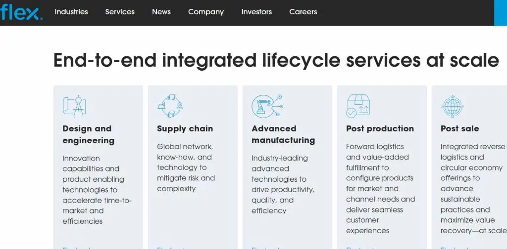
Flex (formerly Flextronics) has continued to thrive by emphasizing its “Sketch-to-Scale” approach, providing end-to-end solutions for clients across various industries. The company’s investments in Industry 4.0 technologies and sustainable manufacturing practices have paid off, attracting environmentally conscious clients.
Headquarters: USA Key Strengths: Advanced manufacturing technologies, strong presence in healthcare and industrial sectors
Jabil has strengthened its position in the EMS market by focusing on high-value sectors such as healthcare, automotive, and industrial equipment. The company’s investments in additive manufacturing and digital supply chain solutions have set it apart from competitors.
Headquarters: USA Key Strengths: High-complexity products, strong presence in defense and aerospace
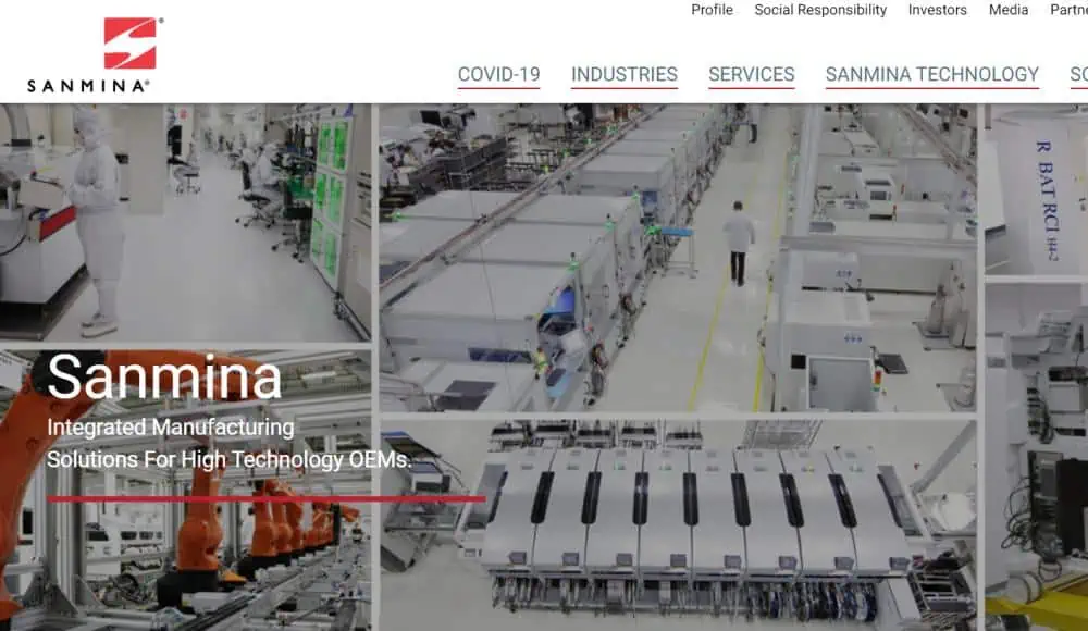
Sanmina has maintained its focus on high-reliability, complex products for demanding industries such as defense, aerospace, and medical devices. By 2026, the company has expanded its capabilities in cybersecurity and advanced materials, catering to the evolving needs of its specialized client base.
Headquarters: USA Key Strengths: Specialized in complex products, strong engineering capabilities
Plexus has continued to excel in serving clients with complex manufacturing requirements. The company’s investments in advanced engineering services and IoT solutions have helped it secure long-term partnerships in growing sectors such as robotics and renewable energy.
Headquarters: USA Key Strengths: Focus on high-reliability markets, strong design services
Benchmark Electronics has maintained its position as a key player in the EMS industry by focusing on high-value, complex products for aerospace, defense, and medical markets. The company’s expansion into IoT and edge computing solutions has opened up new growth opportunities.
Headquarters: Canada Key Strengths: Strong presence in cloud and communications infrastructure, focus on sustainability
Celestica has successfully pivoted towards high-growth markets such as cloud infrastructure, 5G networks, and renewable energy systems. The company’s commitment to sustainable manufacturing practices has resonated well with environmentally conscious clients.
Headquarters: China Key Strengths: Expertise in miniaturization, strong presence in wireless and automotive markets
USI has continued to grow its market share, particularly in the wireless communications and automotive electronics sectors. The company’s advancements in System-in-Package (SiP) technology have made it a preferred partner for clients seeking compact, high-performance solutions.
Headquarters: Germany Key Strengths: Mechatronics expertise, strong presence in European markets
Zollner has maintained its position as a leading EMS provider in Europe, leveraging its expertise in mechatronics and Industry 4.0 technologies. The company’s focus on automotive electronics and smart factory solutions has driven its growth in recent years.
Headquarters: China Key Strengths: Vertical integration, strong presence in mobile devices and automotive electronics
BYD Electronic has continued to expand its EMS offerings, leveraging its parent company’s expertise in battery technology and electric vehicles. The company’s focus on sustainability and green manufacturing has attracted environmentally conscious clients.
Headquarters: Switzerland Key Strengths: Specialization in industrial electronics, strong presence in European markets
Enics has maintained its position as a key player in the industrial electronics sector, with a particular focus on automation, energy, and transportation markets. The company’s investments in digital manufacturing and lifecycle services have strengthened its competitive edge.
Headquarters: Taiwan Key Strengths: Diverse product portfolio, strong presence in consumer electronics and smart home devices
New Kinpo Group has continued to expand its EMS offerings, particularly in the areas of IoT devices, smart home products, and wearable technology. The company’s focus on vertical integration and design services has helped it secure long-term partnerships with major brands.
Headquarters: Japan Key Strengths: Strong presence in automotive and industrial markets, expertise in high-reliability products
Sumitronics has maintained its position as a key EMS provider, particularly in the Japanese market. The company’s focus on automotive electronics, industrial automation, and medical devices has driven its growth in recent years.
Headquarters: Japan Key Strengths: Global presence, expertise in automotive and consumer electronics
SIIX has continued to expand its global footprint, leveraging its strong presence in both Asian and European markets. The company’s focus on automotive electronics and IoT devices has helped it secure new clients and diversify its revenue streams.
Headquarters: Singapore Key Strengths: Expertise in precision engineering, strong presence in medical and automotive markets
Beyonics (formerly BH Electronics) has strengthened its position in the EMS market by focusing on high-precision components for medical devices and automotive applications. The company’s investments in advanced manufacturing technologies have set it apart from competitors.
Headquarters: USA Key Strengths: Specialization in low-volume, high-mix production, strong presence in medical and defense markets
Saline Lectronics has continued to excel in serving clients with complex, low-volume manufacturing requirements. The company’s focus on advanced testing and quality assurance has made it a preferred partner for clients in highly regulated industries.
Headquarters: USA Key Strengths: Expertise in complex assemblies, strong presence in aerospace and defense markets
MC Assembly, now part of Integra Technologies, has maintained its focus on high-reliability, complex assemblies for aerospace, defense, and medical markets. The company’s investments in advanced manufacturing technologies and cybersecurity have strengthened its competitive position.
Headquarters: Sweden Key Strengths: Strong presence in European markets, expertise in industrial and medtech sectors
NOTE has continued to grow its market share in Europe, particularly in the industrial, medtech, and greentech sectors. The company’s focus on digitalization and sustainability has resonated well with its client base.
Headquarters: UK Key Strengths: Expertise in high-reliability markets, strong design and engineering capabilities
TT Electronics has maintained its position as a key player in the EMS industry, focusing on high-reliability markets such as aerospace, defense, and medical devices. The company’s investments in power management and sensor technologies have opened up new growth opportunities.
Headquarters: USA Key Strengths: Vertically integrated services, strong presence in consumer and industrial markets
Key Tronic has continued to offer a wide range of EMS solutions, from design to manufacturing and distribution. The company’s focus on vertical integration and supply chain optimization has helped it maintain long-term relationships with key clients.
Headquarters: France Key Strengths: Global presence, expertise in high-mix, low-volume production
Asteelflash has maintained its position as a leading EMS provider, particularly in Europe and North America. The company’s focus on Industry 4.0 technologies and flexible manufacturing solutions has helped it adapt to changing market demands.
Headquarters: Hong Kong Key Strengths: Expertise in consumer electronics, strong design capabilities
VTech EMS has continued to leverage its parent company’s expertise in consumer electronics, expanding its EMS offerings to include IoT devices, smart home products, and wearable technology. The company’s focus on sustainable manufacturing practices has attracted environmentally conscious clients.
Headquarters: USA Key Strengths: Diverse service offerings, strong presence in industrial and medical markets
Compass Electronics Group has maintained its position as a key player in the EMS industry by offering a wide range of services, from design to manufacturing and lifecycle management. The company’s focus on IoT solutions and digital transformation has driven its growth in recent years.
Headquarters: USA Key Strengths: Flexible manufacturing capabilities, strong presence in consumer and industrial markets
SigmaTron has continued to offer a wide range of EMS solutions, adapting to changing market demands with its flexible manufacturing capabilities. The company’s investments in automation and supply chain optimization have helped it maintain its competitive edge.
Headquarters: USA Key Strengths: Expertise in high-reliability markets, strong engineering capabilities
SMTC has maintained its focus on serving clients in high-reliability markets such as aerospace, defense, and medical devices. The company’s investments in advanced manufacturing technologies and design services have strengthened its position in these specialized sectors.
Headquarters: Philippines Key Strengths: Strong presence in automotive and industrial markets, expertise in power modules
IMI has continued to grow its market share, particularly in the automotive electronics and industrial automation sectors. The company’s focus on power modules and renewable energy solutions has opened up new growth opportunities.
Headquarters: USA Key Strengths: Expertise in aerospace and defense markets, strong engineering capabilities
Ducommun has maintained its position as a key player in the aerospace and defense sectors, leveraging its expertise in complex electronic and structural systems. The company’s investments in advanced materials and manufacturing technologies have set it apart from competitors.
Headquarters: USA Key Strengths: Global presence, expertise in high-mix, low-to-mid volume production
Vexos has continued to offer flexible EMS solutions for clients across various industries, with a particular focus on medical devices, industrial equipment, and communications technology. The company’s investments in supply chain resilience and digital manufacturing have strengthened its competitive position.
Creation Technologies has maintained its focus on serving clients with complex manufacturing requirements, particularly in the medical, aerospace, and defense sectors. The company’s investments in advanced engineering services and digital transformation have helped it secure long-term partnerships with key clients.
Trends Shaping the EMS Industry in 2026
1. Industry 4.0 and Smart Manufacturing
The adoption of Industry 4.0 technologies, such as IoT, AI, and machine learning, has become widespread among top EMS providers. These technologies enable:
Real-time monitoring and optimization of production processes
Environmental concerns have become a top priority for both EMS providers and their clients. Key initiatives include:
Adoption of renewable energy sources in manufacturing facilities
Implementation of circular economy principles in product design and manufacturing
Reduction of carbon footprint through optimized logistics and supply chain management
Use of eco-friendly materials and packaging solutions
3. Reshoring and Regional Manufacturing
The global pandemic and geopolitical tensions have accelerated the trend towards reshoring and regional manufacturing. EMS providers are:
Establishing or expanding facilities closer to end markets
Implementing flexible manufacturing solutions to adapt to changing demand
Diversifying supply chains to reduce dependency on single regions or suppliers
4. Specialization and Value-Added Services
Top EMS companies are differentiating themselves by offering specialized services and moving up the value chain:
Advanced design and engineering services
Prototyping and new product introduction (NPI) support
Lifecycle management and aftermarket services
Regulatory compliance and certification support
5. Cybersecurity and Data Protection
As manufacturing becomes increasingly digital, cybersecurity has become a critical concern for EMS providers:
Implementation of robust cybersecurity measures in manufacturing processes
Secure data management and protection of intellectual property
Compliance with evolving data protection regulations
Offering cybersecurity services as part of product design and manufacturing
Conclusion
The Electronic Manufacturing Services industry continues to evolve rapidly, driven by technological advancements, changing market demands, and global challenges. The top 30 EMS companies in 2026 have demonstrated their ability to adapt to these changes, investing in new technologies, expanding their service offerings, and focusing on sustainability.
As we look towards the future, the most successful EMS providers will be those that can balance global reach with regional responsiveness, leverage advanced technologies to improve efficiency and quality, and offer value-added services that go beyond traditional manufacturing. The industry’s role in bringing innovative products to market quickly and efficiently will only grow in importance as technology continues to shape our world.
For companies seeking EMS partners, this list of top 30 providers offers a starting point for evaluating potential collaborators. However, it’s crucial to consider your specific needs, industry requirements, and long-term goals when selecting an EMS provider. The right partnership can be a key driver of innovation, efficiency, and success in today’s competitive technology landscape.
To enhance the efficiency of PCB manufacturing and assembly, we highly recommend utilizing panel designs. Panelization not only streamlines the production process but also helps reduce assembly costs.
The minimum panel size for assembly is 50x50mm, while the maximum can go up to 330x530mm. You have the option to provide your own panel design, or we can create one for you based on your specific requirements. When submitting a new order on PCBWay, simply include your panel design preferences in the message section.
Panel with V-Cut/V-Scoring/V-Groove
For V-scoring panelization, the spacing between boards can be either 0mm or 3mm. Below are reference images for your guidance:
By opting for panelization, you can significantly improve production efficiency and cost-effectiveness. Let us know your panel design needs, and we’ll ensure your PCBs are manufactured and assembled to the highest standards.
Panel with V-Cut,V-Scoring,V-Groove
V-scoring has to be continuous and can not be stopped in panel, if you have many different boards like following image to be panelized, we suggest add tab routes between boards instead of V-scoring.
Panel with Tab Routing
For panels utilizing tab routing, a 1.6mm spacing is required between boards. There are two types of tab routing commonly used in panelization:
Tab routing with breaking holes (stamp holes)
Tab routing with tabs (no holes)
1. Tab Routing with Breaking Holes (Stamp Holes)
The diameter of the breaking holes should be ≥0.45mm, with a typical range of 0.55mm-0.6mm.
The spacing between holes must be ≥0.35mm.
Typically, 5-6 holes are added to each tab for optimal strength and ease of separation.
Refer to the following image for a visual example:
Tab route with breaking holes
2. Tab Routing with Tabs (No Holes)
The width of each tab must be at least 2mm.
Refer to the following image for a visual example:
Tab route with tab(no holes)
Panel with Both V-Scoring and Tab Routing
For panels combining V-scoring and tab routing:
The spacing in the V-scoring area should be 3mm.
The spacing in the tab routing area should be 1.6mm.
Refer to the following image for a visual example:
Panel with both V-scoring and tab routes
Fiducial Marks and Mounting Holes in Panels
Fiducial Marks
Fiducial marks are essential for assembly alignment.
Typically, 3 fiducial marks are added to each panel.
Efficient Testing and Debugging: Facilitates faster and more accurate testing.
For high-volume PCB assembly, array panelization is an excellent choice. Partnering with a trusted PCB assembly service provider like RayMing PCB can ensure your project meets the highest standards. Contact us today to discuss your panelization needs or to learn more about the benefits of array panelization for high-volume PCB assembly.