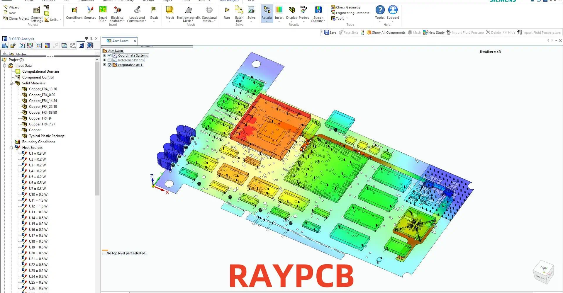
Express PCB and Express SCH represent a powerful combination of circuit design tools that have become popular among electronics engineers, hobbyists, and professional designers. This comprehensive guide explores both software packages, their features, capabilities, and how they work together to streamline the electronic design process.
Q1: Can Express PCB and Express SCH files be exported to other CAD software?
A1: Express PCB and Express SCH use proprietary file formats, but they offer limited export capabilities. Schematics can be exported as PDF or image files, while PCB designs can be exported as Gerber files for manufacturing. However, direct conversion to other CAD formats is not supported.
Q2: What are the limitations of the free version compared to the paid versions?
A2: The free version includes basic schematic and PCB design capabilities but has limitations on:
Board size (maximum 4″ x 4″)
Layer count (2 layers maximum)
Export options (limited file formats)
Advanced features (no auto-routing or DRC) Paid versions remove these restrictions and add professional features.
Q3: How does the auto-routing capability compare to other PCB design software?
A3: Express PCB’s auto-routing functionality is basic compared to professional tools like Altium or KiCad. It works well for simple designs but may struggle with:
High-density boards
Complex routing rules
Mixed-signal designs Manual routing is recommended for critical signals and complex layouts.
Q4: Can I create custom component libraries in Express SCH and PCB?
A4: Yes, both Express SCH and PCB support custom component creation. The process involves:
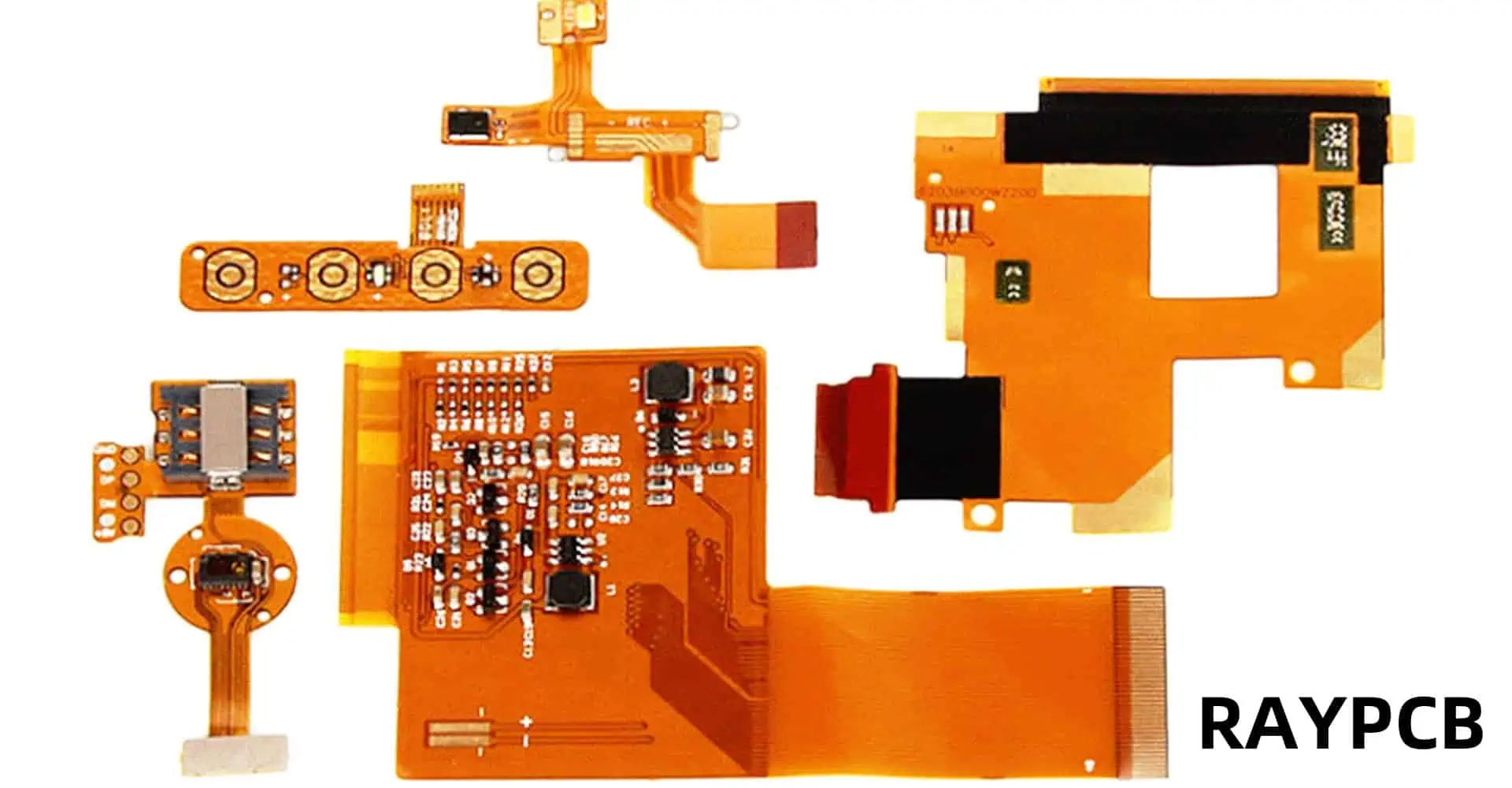
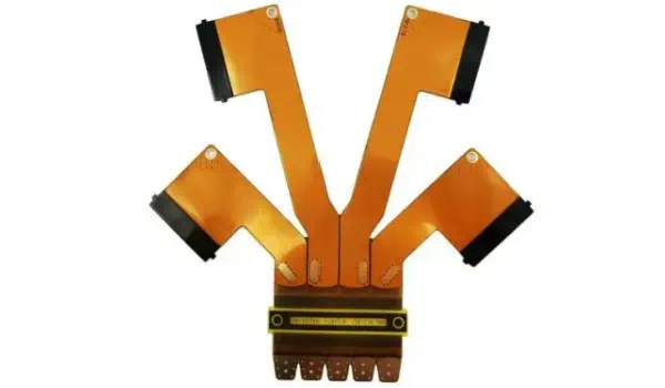
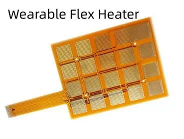
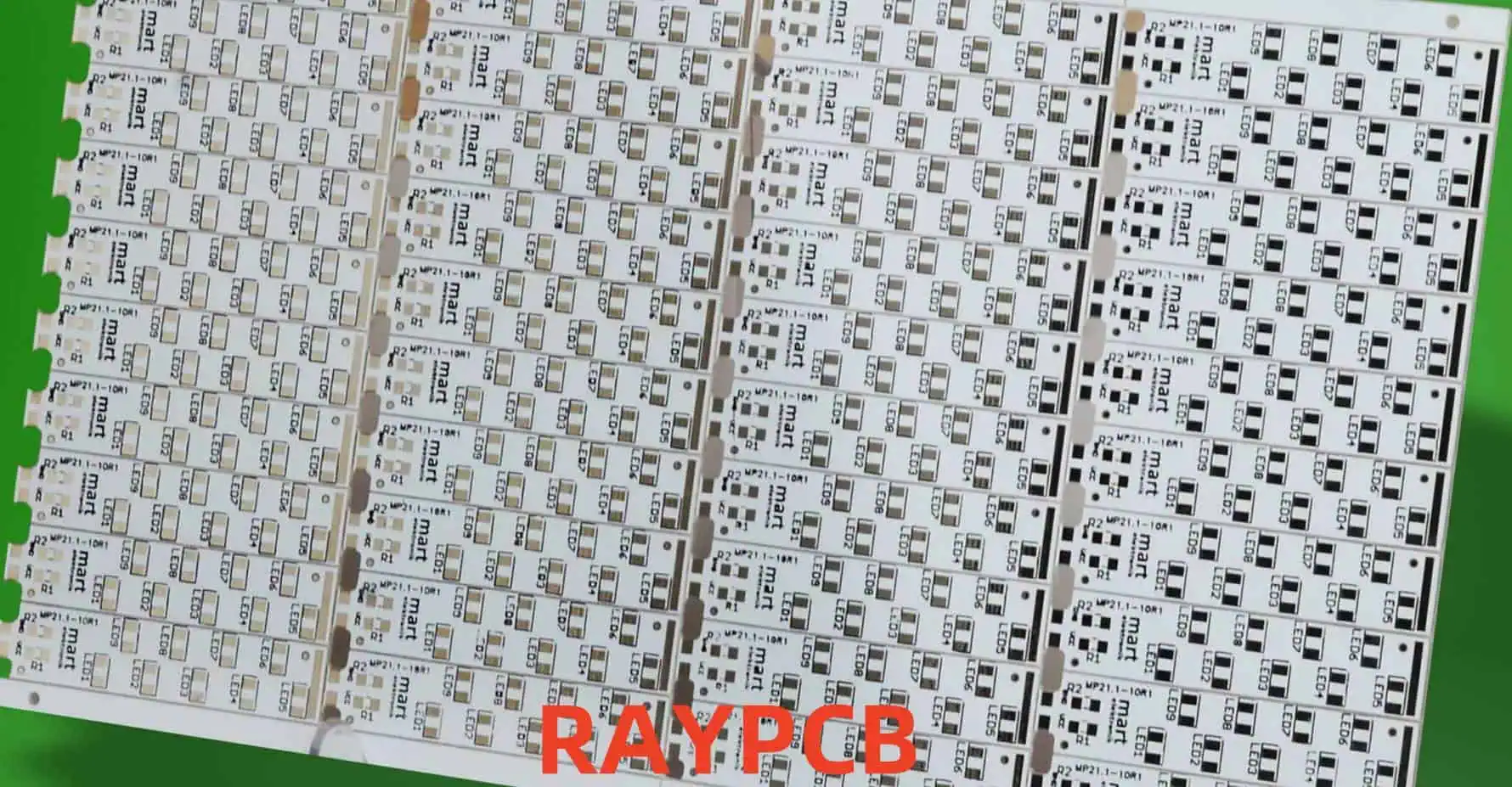
Flexible printed circuit boards, also known as flex PCBs or flexible electronics, are thin, bendable circuit boards that can be shaped to fit into tight spaces or conform to unique product designs. Unlike traditional rigid PCBs, flexible PCBs are made with a flexible base material, typically a plastic film like polyimide, which allows them to bend, fold, and twist without breaking.
Flexible PCBs come in various types, each designed to meet specific application requirements:
Single-sided Flex PCBs
Single-sided flex PCBs have a single conductive layer on one side of the flexible substrate. They are the simplest and most cost-effective type of flexible PCB.
Double-sided Flex PCBs
Double-sided flex PCBs have conductive layers on both sides of the substrate, allowing for more complex circuit designs and higher component density.
Multilayer Flex PCBs
Multilayer flex PCBs consist of three or more conductive layers, separated by insulating layers. They offer the highest level of circuit density and complexity.
Rigid-Flex PCBs
Rigid-flex PCBs combine both rigid and flexible board technologies in a single circuit board. They feature areas of flexible circuitry connected to rigid board sections.
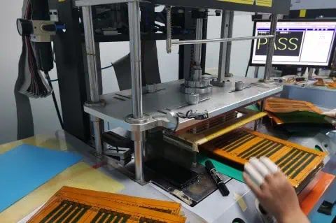
The manufacturing process for flexible PCBs differs from that of rigid PCBs due to the unique materials and requirements involved. Here’s an overview of the main steps:
Each of these steps requires specialized equipment and techniques to ensure the flexibility and durability of the final product.
Advantages of Flexible PCBs
Flexible PCBs offer numerous advantages over their rigid counterparts:
1. Space and Weight Savings
Flexible PCBs can be bent, folded, or shaped to fit into tight or irregularly shaped spaces, allowing for more compact and lightweight product designs.
2. Increased Reliability
The ability to flex reduces stress on components and solder joints, potentially increasing the overall reliability and lifespan of the device.
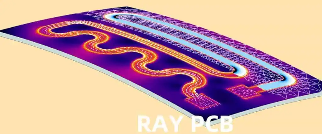
3. Improved Thermal Management
Flexible PCBs can dissipate heat more effectively than rigid boards, which can lead to better thermal management in electronic devices.
4. Enhanced Design Freedom
Designers have more freedom to create unique and innovative product shapes and form factors when using flexible PCBs.
5. Resistance to Vibration and Movement
The flexible nature of these PCBs makes them more resistant to vibration and movement, which is crucial in applications like automotive electronics or wearable devices.
Careful design of flex zones, use of strain relief
Thermal Management
Heat dissipation in dense circuits
Improved thermal design, use of heat-spreading materials
Future of Flexible PCBs
The future of flexible PCBs looks promising, with ongoing research and development pushing the boundaries of what’s possible:
Stretchable Electronics
Researchers are working on developing stretchable PCBs that can not only bend but also stretch, opening up new possibilities for wearable and medical devices.
Integration with 3D Printing
Advancements in 3D printing technology may allow for the direct printing of flexible circuits, potentially revolutionizing the manufacturing process.
Improved Materials
New materials are being developed to enhance the performance, durability, and flexibility of PCBs while potentially reducing costs.
Internet of Things (IoT) and Smart Devices
The growth of IoT and smart devices will likely drive further innovation in flexible PCB technology to meet the demand for smaller, more versatile electronics.
Sustainable and Biodegradable PCBs
As environmental concerns grow, there’s increasing research into developing sustainable and even biodegradable flexible PCBs.
Conclusion
Flexible PCBs have indeed revolutionized the electronics industry, enabling the creation of smaller, lighter, and more versatile devices. While they come with their own set of challenges, the advantages they offer in terms of design freedom, reliability, and performance make them an invaluable technology in modern electronics. As research continues and new applications emerge, we can expect to see even more innovative uses of flexible PCBs in the future, further blurring the lines between rigid and flexible electronics.
FAQ
1. Are flexible PCBs more expensive than rigid PCBs?
Yes, flexible PCBs are generally more expensive than rigid PCBs due to the specialized materials and manufacturing processes involved. However, they can offer cost savings in other areas, such as assembly and packaging, due to their space-saving and design flexibility benefits.
2. How durable are flexible PCBs?
Flexible PCBs are designed to be quite durable and can withstand repeated bending and flexing. However, their durability depends on factors such as the materials used, the design of the flex zones, and the specific application. When properly designed and used within their specified parameters, flexible PCBs can be very reliable.
3. Can all electronic components be used with flexible PCBs?
Not all electronic components are suitable for use with flexible PCBs. Some components may be too rigid or heavy, which could cause stress on the flexible substrate. However, many components have been adapted for use with flexible PCBs, and new flex-compatible components are continually being developed.
4. What industries benefit most from flexible PCB technology?
While flexible PCBs have applications across many industries, they are particularly beneficial in consumer electronics, automotive, medical devices, aerospace, and wearable technology. These industries often require compact, lightweight, and uniquely shaped electronic solutions that flexible PCBs can provide.
5. Is it possible to repair a flexible PCB?
Repairing flexible PCBs can be challenging due to their thin and flexible nature. While minor repairs are possible in some cases, it often requires specialized equipment and expertise. In many situations, especially with mass-produced consumer electronics, it may be more practical to replace the entire flexible PCB rather than attempt a repair.
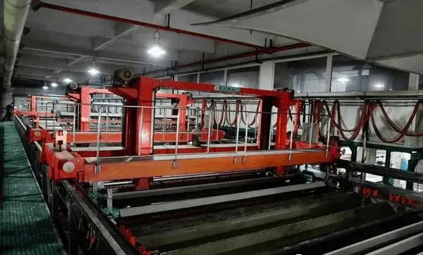
Electroplated nickel has become an integral part of modern printed circuit board (PCB) manufacturing, offering enhanced durability, conductivity, and corrosion resistance. This comprehensive guide explores the technical aspects, processes, and considerations involved in nickel electroplating for PCBs, providing manufacturers and engineers with essential information for optimal implementation.
Understanding Nickel Electroplating Fundamentals
Basic Principles of Electroplating
Electroplating is an electrochemical process where metal ions in solution are reduced to their metallic form on a conductive substrate. In PCB manufacturing, nickel electroplating involves depositing a controlled thickness of nickel onto copper traces and pads, creating a robust protective and functional layer.
Chemical Composition of Plating Solutions
The success of nickel electroplating largely depends on the composition of the plating bath. Modern nickel plating solutions typically contain:
Component
Concentration Range
Function
Nickel Sulfate
200-300 g/L
Primary source of nickel ions
Nickel Chloride
30-60 g/L
Improves anode dissolution
Boric Acid
30-45 g/L
pH buffer
Brighteners
0.5-2 mL/L
Enhance deposit appearance
Levelers
1-3 mL/L
Improve thickness distribution
Process Parameters and Control
Critical Operating Conditions
Maintaining precise control over operating parameters is essential for achieving high-quality nickel deposits:
Q1: What is the optimal thickness for nickel plating on PCB components?
A1: The optimal thickness typically ranges from 2 to 5 micrometers, depending on the application. Critical factors include the expected operating environment, mechanical stress requirements, and subsequent plating layers. For most commercial applications, 3 micrometers provides adequate protection and performance.
Q2: How can I prevent nickel plating adhesion failures?
A2: Adhesion failures can be prevented through proper surface preparation, including thorough cleaning, microetching, and acid activation. Maintaining optimal bath chemistry and ensuring proper current distribution are also critical. Regular Hull cell testing helps identify potential adhesion issues before they occur in production.
Q3: What are the main factors affecting nickel deposit stress?
A3: The primary factors affecting nickel deposit stress include:
Bath temperature
Current density
pH level
Brightener concentration
Impurity levels Controlling these parameters within specified ranges helps minimize internal stress in the deposit.
Q4: How often should the plating bath be analyzed and maintained?
A4: Complete bath analysis should be performed weekly, with basic parameters (pH, temperature, specific gravity) checked daily. Brightener analysis should be conducted every shift, and carbon treatment should be performed monthly or as needed based on organic contamination levels.
Q5: What are the environmental considerations for nickel plating operations?
A5: Key environmental considerations include:
Proper waste treatment and disposal
Recovery and recycling of nickel from rinse waters
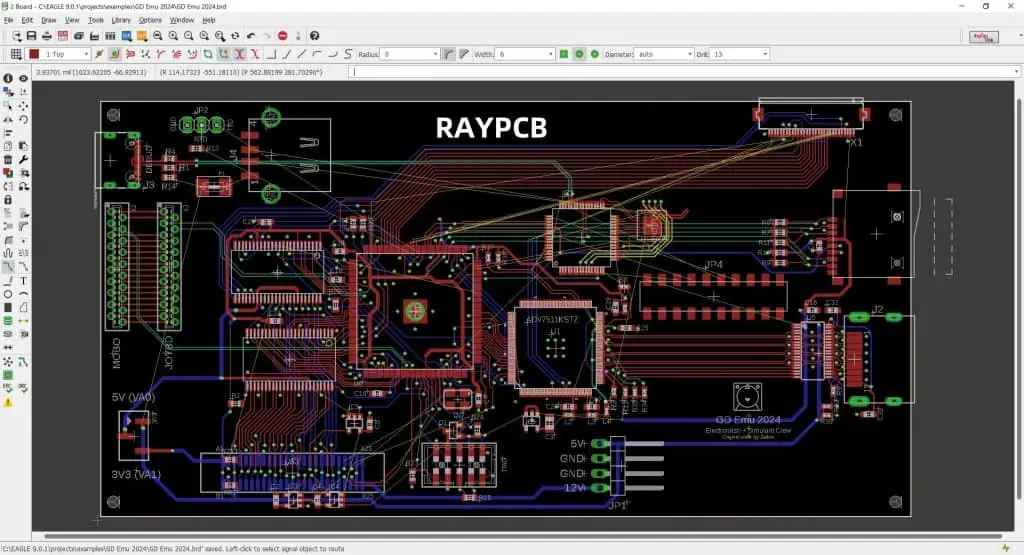
Autodesk EAGLE is a powerful PCB design software that includes essential features for ensuring design quality through Design Rule Check (DRC) and manufacturing preparation via Gerber file generation. This comprehensive guide explores both aspects in detail, providing crucial information for PCB designers and engineers.
Component library problems Always verify component libraries and design rules match your project requirements.
Q3: How can I verify my Gerber files are correct before sending them to manufacturing?
Use these steps:
View files in a Gerber viewer
Check all layer alignments
Verify board dimensions
Confirm drill file accuracy
Compare against original design
Q4: What’s the difference between outline and dimension layers in Gerber export?
The dimension layer (20) defines the physical board outline for manufacturing, while outline layers can be used for documentation or assembly information. Always use the dimension layer for the actual board outline in Gerber export.
Q5: How often should I run DRC checks during PCB design?
Best practices recommend:
After placing major components
During routing (incremental checks)
Before starting a new design section
Before generating Gerber files
After any significant design changes Regular checks help catch issues early in the design process.
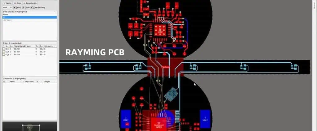
DipTrace is a powerful PCB design software suite that enables engineers and designers to create professional-grade printed circuit boards. One of its crucial features is the ability to export designs to Gerber format, the de facto standard for PCB manufacturing. This comprehensive guide explores DipTrace’s capabilities and the intricacies of Gerber file export.
Q1: Why are my Gerber files missing some PCB features?
This usually occurs due to incorrect layer selection or export settings. Ensure all necessary layers are selected and properly configured in the export dialog. Also, verify that all features are on their correct layers in the PCB design.
Q2: How can I verify my Gerber files before sending them to manufacturing?
Use a Gerber viewer software to check all layers, ensure proper alignment, and verify dimensions. Popular viewers include GerbView, CAM350, or online viewers provided by PCB manufacturers. DipTrace also includes a built-in preview feature.
Q3: What’s the difference between RS-274X and RS-274D Gerber formats?
RS-274X is the newer, extended format that includes aperture definitions within the file, making it more self-contained. RS-274D is older and requires separate aperture files. DipTrace primarily uses RS-274X for better compatibility with modern manufacturing processes.
Q4: Why do I need to include a drill file with my Gerber files?
The drill file (.TXT or .XLN) contains essential information about hole locations, sizes, and types that isn’t included in the Gerber layers. This file is crucial for the PCB manufacturer to properly drill all holes in your board.
Q5: How can I optimize my Gerber export process for complex boards?
Create a checklist including:
Layer verification
DRC completion
Export settings confirmation
File naming conventions
Post-export verification This ensures consistency and reduces errors in the export process.
In the realm of electronic components and circuit design, Printed Circuit Boards (PCBs) and Integrated Circuits (ICs) are fundamental elements that have revolutionized modern electronics. While both serve crucial roles in electronic devices, they differ significantly in their design, functionality, and applications. This comprehensive guide explores the key differences between PCBs and ICs, their manufacturing processes, applications, and the crucial role they play in modern electronics.
Understanding PCB (Printed Circuit Board)
Definition and Basic Structure
A Printed Circuit Board (PCB) is a flat board made of non-conductive material that provides mechanical support and electrical connections for electronic components through conductive pathways, or traces, etched from copper sheets laminated onto the board.
An Integrated Circuit is a miniaturized electronic circuit containing thousands or millions of electronic components (transistors, resistors, capacitors) fabricated on a single semiconductor material, typically silicon.
Yes, PCBs often serve as the platform for mounting and connecting multiple ICs along with other electronic components. The PCB provides the necessary interconnections between ICs and other components while offering mechanical support.
Q2: Why can’t ICs be repaired like PCBs?
ICs cannot typically be repaired because their components are microscopic and integrated into a single piece of semiconductor material. PCBs, on the other hand, have larger, discrete components that can be replaced individually.
Q3: Which is more cost-effective for mass production?
For mass production, ICs are generally more cost-effective per unit despite having higher initial setup costs. PCBs have lower setup costs but higher per-unit costs in large volumes.
Q4: Can PCBs be designed without ICs?
Yes, Prototype PCBs can be designed using discrete components without ICs, but modern electronic devices typically use a combination of both for optimal performance and functionality.
Q5: What determines the choice between using a PCB or an IC for a specific function?
Aluminum PCBs (Metal Core PCBs or MCPCBs) have become increasingly important in high-power electronic applications due to their superior thermal management capabilities. This article explores the fundamentals of heat dissipation in aluminum PCBs and presents comprehensive design methodologies for optimal thermal performance.
Aluminum PCB design for optimal heat dissipation requires careful consideration of material selection, layout design, and manufacturing processes. Success depends on understanding thermal management principles and implementing appropriate design methodologies. Regular testing and validation ensure that thermal performance meets design requirements. As power densities continue to increase, the importance of effective thermal management in aluminum PCBs will only grow.
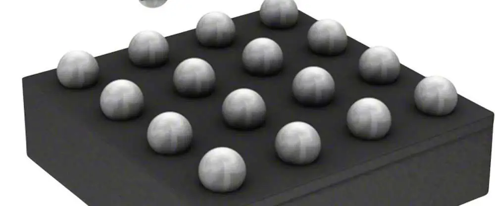
Ball Grid Array (BGA) solderability is crucial for ensuring reliable electronic assemblies. This comprehensive guide covers industry standards, testing methods, acceptance criteria, and best practices for BGA soldering processes. Understanding and implementing these standards is essential for achieving high-quality, reliable electronic assemblies.
Maintaining high standards for BGA solderability is essential for producing reliable electronic assemblies. Following these guidelines and standards helps ensure consistent quality and reliability in BGA assembly processes. Regular monitoring, documentation, and process control are key to maintaining these standards. As technology continues to evolve, staying current with the latest standards and best practices remains crucial for successful BGA assembly operations.
In today’s electronic design landscape, choosing the right PCB design and EDA simulation tool is crucial for successful project completion. This comprehensive comparison examines popular tools, their capabilities, strengths, and limitations to help engineers and designers make informed decisions for their specific needs.
A1: KiCad is often recommended for beginners due to its free availability, extensive documentation, active community support, and relatively gentle learning curve. It offers all essential features needed to complete basic to intermediate PCB designs while providing a pathway to more advanced capabilities as skills develop.
Q2: How do commercial tools justify their high costs compared to open-source alternatives?
A2: Commercial tools justify their costs through advanced features like integrated simulation capabilities, professional technical support, automated design rule checking, advanced routing algorithms, and enterprise-level integration capabilities. They often provide time-saving features that can significantly reduce design cycle time in professional environments.
Q3: What factors should be considered when choosing between different EDA tools?
A3: Key factors include:
Project complexity and requirements
Budget constraints
Team size and collaboration needs
Required integration with other tools
Available computing resources
Learning curve and training requirements
Long-term maintenance and support needs
Q4: How do different tools handle high-speed design requirements?
A4: Professional tools like Altium, OrCAD, and PADS provide advanced high-speed design features including controlled impedance routing, length matching, differential pair routing, and integrated signal integrity analysis. Open-source tools may require external tools or plugins for advanced high-speed design capabilities.
Q5: What are the key differences in simulation capabilities between various tools?
A5: Professional tools typically offer integrated simulation capabilities for signal integrity, power integrity, and EMI analysis. Tools like HyperLynx and ADS provide more advanced simulation capabilities but require separate licenses. Open-source tools often rely on external simulation tools or limited built-in capabilities.
Conclusion
The choice of PCB design and EDA simulation tools depends heavily on specific project requirements, budget constraints, and team capabilities. While commercial tools offer comprehensive features and professional support, open-source alternatives provide capable solutions for many applications. Understanding the strengths and limitations of each tool is crucial for making an informed decision that aligns with project needs and organizational capabilities.
The trend towards cloud-based tools and integrated design environments continues to shape the landscape of PCB design tools, with increasing emphasis on collaboration features and integration capabilities. Regular evaluation of available tools and their evolving capabilities remains important for maintaining competitive advantage in electronic design.
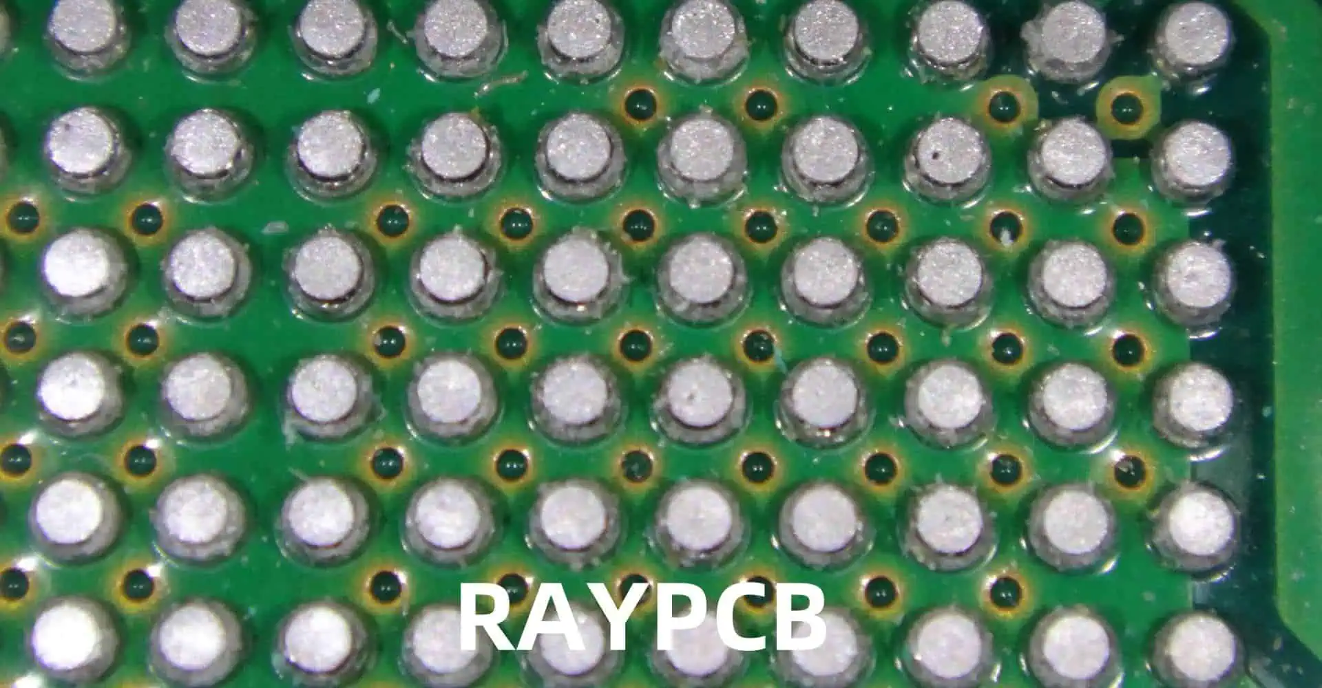
The increasing demand for miniaturization in electronic devices has led to the widespread adoption of 0201 components and microBall Grid Array (BGA) packages. Understanding and managing PCB tolerances for these ultra-small components is crucial for successful assembly and reliable product performance. This comprehensive guide explores the critical aspects of PCB design, manufacturing tolerances, and best practices for working with 0201 components and micro BGAs.
Understanding 0201 Components
Dimensional Specifications
0201 components represent one of the smallest surface mount device (SMD) form factors available in mass production. The designation “0201” refers to the imperial measurements:
Dimension
Imperial (inches)
Metric (mm)
Length
0.024 ± 0.002
0.60 ± 0.05
Width
0.012 ± 0.001
0.30 ± 0.03
Height
0.006 ± 0.001
0.15 ± 0.03
Terminal
0.008 ± 0.001
0.20 ± 0.03
Critical Tolerance Considerations
Pad Design Parameters
DSBGA
The pad design for 0201 components requires precise control of several key parameters:
Q1: What is the minimum recommended trace width for routing under micro BGAs?
A1: The minimum recommended trace width for routing under micro BGAs is 0.075mm (3 mils). However, it’s important to consider manufacturing capabilities and impedance requirements when selecting final trace dimensions.
Q2: How does moisture sensitivity affect micro BGA assembly?
A2: Moisture sensitivity can lead to package cracking during reflow if proper handling procedures aren’t followed. Components should be stored in moisture barrier bags with desiccant and humidity indicators, and floor life limitations must be strictly observed based on the MSL level.
Q3: What are the key considerations for selecting PCB surface finish for 0201 and micro BGA applications?
A3: ENIG or ENEPIG are preferred surface finishes due to their excellent planarity, solderability, and shelf life. These finishes provide consistent solderability and help prevent oxidation issues during assembly.
Q4: How can void percentage in micro BGA solder joints be minimized?
A4: Void percentage can be minimized through proper reflow profile optimization, using quality solder paste, implementing appropriate pad designs, and ensuring proper storage and handling of components and materials.
Q5: What are the recommended inspection methods for 0201 components and micro BGAs?
A5: A combination of AOI, X-ray inspection, and SPI (Solder Paste Inspection) is recommended. AOI can verify component placement and presence, X-ray inspection can check solder joint quality and void content, while SPI ensures proper solder paste deposit volume and position.
Conclusion
Successfully implementing 0201 components and micro BGAs requires careful attention to PCB design tolerances, manufacturing processes, and quality control measures. By following the guidelines and specifications outlined in this document, engineers can achieve reliable and consistent assembly results. Regular review and updates of these parameters based on production feedback and new technology developments will help maintain high-quality standards in electronic assembly.