Laser Depaneling PCB: How to Depanelize Round Ceramic PCB

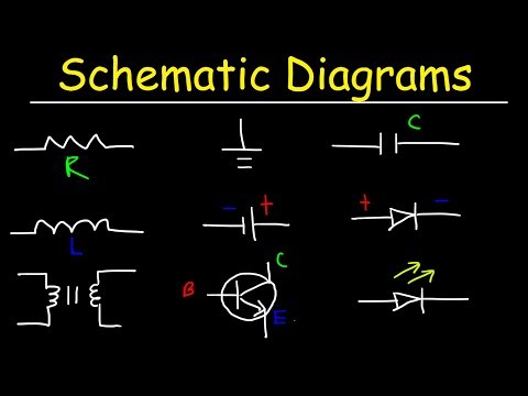
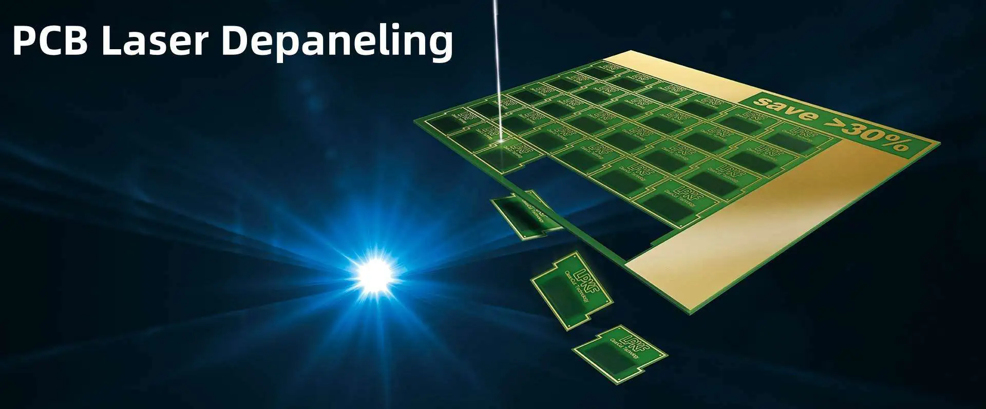
What is Laser Depaneling?

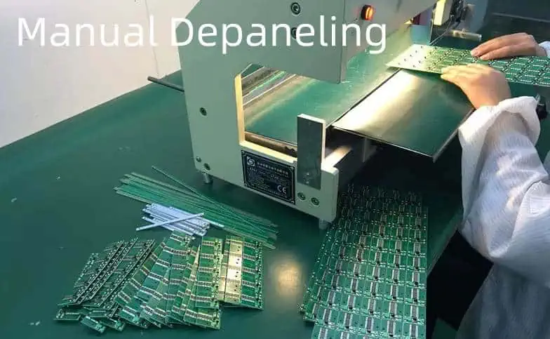
Laser depaneling is a cutting-edge technology that uses a focused laser beam to separate individual PCBs from a larger panel. This method offers numerous advantages over traditional mechanical depaneling techniques, especially when dealing with delicate or uniquely shaped PCBs like round ceramic boards.

The Science Behind Laser Depaneling

Laser depaneling works on the principle of material ablation. The laser beam, typically a CO2 or UV laser, is focused on the PCB material, vaporizing it along a predetermined path. This process creates a clean, precise cut without applying mechanical stress to the board.

YouTube video

Key Components of a Laser Depaneling System

  1. Laser Source
  2. Beam Delivery System
  3. Motion Control System
  4. Vision System
  5. Exhaust and Filtration System

Advantages of Laser Depaneling for Round Ceramic PCBs

  1. Precision: Laser cutting offers unparalleled accuracy, crucial for round shapes.
  2. Stress-Free: No mechanical stress is applied to the delicate ceramic material.
  3. Clean Cuts: Laser cutting produces smooth edges without debris.
  4. Flexibility: Easily adaptable for various board shapes and sizes.
  5. Programmability: Can be quickly reprogrammed for different designs.

Preparing for Laser Depaneling of Round Ceramic PCBs

Material Considerations

Ceramic PCBs have unique properties that make them ideal for certain applications but also require special handling during the depaneling process.

Properties of Ceramic PCBs

PropertyCharacteristicImplication for Depaneling
Thermal ConductivityHighRequires careful power adjustment
BrittlenessHighProne to chipping if mishandled
Dielectric ConstantHighExcellent for RF applications
Coefficient of Thermal ExpansionLowLess warping during laser cutting

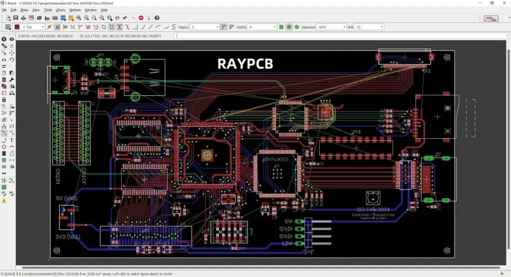
Design Considerations for Laser Depaneling

When designing round ceramic PCBs for laser depaneling, several factors should be taken into account:

  1. Panel Layout
  2. Depaneling Path Design
  3. Tab Design (if applicable)
  4. Fiducial Marks for Alignment

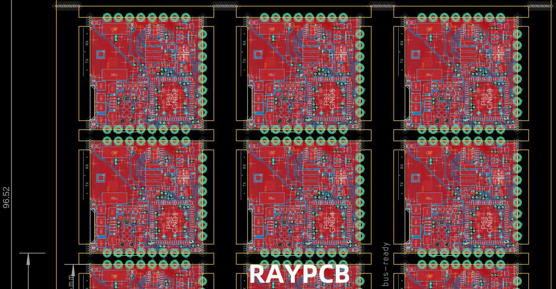
Optimal Panel Layout for Round Ceramic PCBs

Layout TypeEfficiencyWaste MaterialRecommended for
Grid LayoutMediumMediumSmall to medium runs
Honeycomb LayoutHighLowLarge production runs
Circular ArrayHighLow-MediumMaximizing space utilization

The Laser Depaneling Process for Round Ceramic PCBs

Step 1: Machine Setup and Calibration

Before beginning the depaneling process, it’s crucial to properly set up and calibrate the laser system:

  1. Laser Power Calibration
  2. Focus Adjustment
  3. Alignment Verification
  4. Test Cuts on Scrap Material

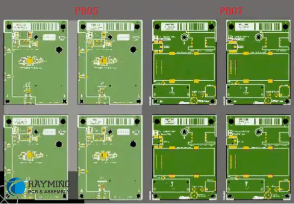
Step 2: Loading the PCB Panel

Proper loading of the round ceramic PCB panel is essential for accurate depaneling:

  1. Clean the work surface
  2. Secure the panel using appropriate fixtures
  3. Ensure the panel is flat and level

Step 3: Programming the Cutting Path

For round ceramic PCBs, the cutting path must be precisely programmed:

  1. Import the PCB design file
  2. Define the cutting path along the circumference
  3. Set laser parameters (power, speed, frequency)
  4. Optimize the cutting sequence

Typical Laser Parameters for Ceramic PCB Depaneling

ParameterRangeNotes
Laser Power20-100WDepends on material thickness
Cutting Speed10-50 mm/sSlower for thicker materials
Pulse Frequency20-50 kHzHigher for smoother edges
Number of Passes1-3Multiple passes for thicker boards

Step 4: Executing the Depaneling Process

Once everything is set up and programmed, the actual depaneling process can begin:

  1. Initiate the laser cutting sequence
  2. Monitor the process for any irregularities
  3. Allow for proper cooling between cuts if necessary

Step 5: Post-Depaneling Inspection and Cleaning

After the depaneling is complete, thorough inspection and cleaning are crucial:

  1. Visual inspection for any defects or incomplete cuts
  2. Edge quality check
  3. Removal of any dust or debris
  4. Functional testing of depaneled PCBs

Optimizing Laser Depaneling for Round Ceramic PCBs

Fine-Tuning Laser Parameters

Achieving the best results often requires fine-tuning the laser parameters:

  1. Adjusting laser power for different board thicknesses
  2. Optimizing cutting speed for clean edges
  3. Experimenting with pulse frequency for minimal heat affected zone

Handling Challenges Specific to Round Ceramic PCBs

Round ceramic PCBs present unique challenges that require specific strategies:

  1. Ensuring uniform cutting around the circumference
  2. Dealing with potential chipping at the edges
  3. Managing heat distribution during cutting

Implementing Quality Control Measures

To maintain high-quality output, implement robust quality control measures:

  1. Regular calibration checks
  2. Periodic test cuts on sample materials
  3. Documentation of optimal parameters for different board specifications

Advanced Techniques for Laser Depaneling Round Ceramic PCBs

Multi-Pass Cutting

For thicker ceramic PCBs, multi-pass cutting can be employed:

  1. Divide the total cut depth into multiple passes
  2. Adjust laser power and speed for each pass
  3. Allow cooling time between passes

Combination with Other Techniques

In some cases, laser depaneling can be combined with other methods for optimal results:

  1. Pre-scoring the ceramic material
  2. Using controlled fracture techniques for final separation
  3. Implementing robotic handling for improved efficiency

Environmental and Safety Considerations

Laser depaneling of ceramic PCBs requires attention to environmental and safety aspects:

  1. Proper ventilation and filtration systems
  2. Laser safety protocols and protective equipment
  3. Proper disposal of ceramic dust and debris

Future Trends in Laser Depaneling for Ceramic PCBs

The field of laser depaneling continues to evolve:

  1. Integration with Industry 4.0 and IoT
  2. Development of more efficient and powerful laser sources
  3. Advancements in automated handling and inspection systems

Conclusion

Laser depaneling of round ceramic PCBs represents a significant advancement in PCB manufacturing technology. By offering precision, flexibility, and stress-free separation, it enables the production of high-quality, complex PCB designs. As the electronics industry continues to demand more sophisticated and compact designs, the role of laser depaneling in PCB manufacturing is set to become increasingly important.

FAQ

Q1: Is laser depaneling suitable for all types of ceramic PCBs?

A1: While laser depaneling is suitable for most ceramic PCBs, the specific parameters may need adjustment based on the type of ceramic material, thickness, and board design. It’s particularly effective for round ceramic PCBs due to its precision in cutting curved paths.

Q2: How does the cost of laser depaneling compare to traditional methods?

A2: Initially, the setup cost for laser depaneling can be higher than traditional methods. However, it often proves more cost-effective in the long run, especially for high-volume production or when working with complex or delicate designs like round ceramic PCBs.

Q3: Are there any limitations to the thickness of ceramic PCBs that can be laser depaneled?

A3: While laser depaneling can handle a wide range of thicknesses, extremely thick ceramic PCBs may require multiple passes or a combination of techniques. The maximum thickness depends on the power of the laser and the specific properties of the ceramic material.

Q4: How does laser depaneling affect the electrical properties of ceramic PCBs?

A4: When done correctly, laser depaneling has minimal impact on the electrical properties of ceramic PCBs. The heat-affected zone is typically very small, and the process doesn’t introduce mechanical stress that could affect the board’s performance.

Q5: What maintenance is required for a laser depaneling system?

A5: Regular maintenance of a laser depaneling system typically includes cleaning of optics, checking and replacing filters, calibrating the laser and motion control systems, and inspecting for any wear or damage to components. The frequency of maintenance depends on usage but is generally less intensive than mechanical depaneling systems.

Creating Schematic Symbols from CSV Files: A Comprehensive Technical Guide

Schematic Symbols

The Importance of Automated Symbol Creation

In the rapidly evolving world of electronic design, efficient methods for generating schematic symbols are crucial. CSV (Comma-Separated Values) files offer a powerful and flexible approach to streamline the symbol creation process across various electronic design automation (EDA) platforms.

YouTube video

Fundamentals of Schematic Symbol Generation

Understanding CSV-Based Symbol Creation

Key Components of Symbol Generation

ComponentDescriptionSignificance
CSV StructureData OrganizationDefines Symbol Attributes
Parsing MechanismData ExtractionTranslates CSV to Symbol Properties
Symbol Generation AlgorithmConversion LogicTransforms Data into Graphical Representation
EDA IntegrationCompatibility LayerEnsures Cross-Platform Functionality

CSV File Preparation

Optimal CSV Structure for Schematic Symbols

Recommended CSV Column Configurations

Column NameTypical ContentPurpose
ComponentNameUnique IdentifierPrimary Component Reference
PinNameInput/Output Pin NamesDefines Connection Points
PinTypeSignal DirectionInput, Output, Bidirectional
PinNumberPhysical Pin LocationCoordinate Mapping
ElectricalTypeSignal CharacteristicsAnalog, Digital, Power

Data Validation Techniques

Comprehensive Validation Strategies

Validation TypeCheck ParametersVerification Method
Structural IntegrityColumn ConsistencyAutomated Parsing
Naming ConventionsStandardized NamingRegex Pattern Matching
Value RangesAcceptable Pin ConfigurationsPredefined Constraint Checking

Programming Approaches for Symbol Generation

Systematic Symbol Creation Methodologies

Symbol Generation Workflow

  1. CSV File Parsing
  2. Data Normalization
  3. Symbol Geometry Calculation
  4. EDA-Specific Formatting
  5. Validation and Export

Programming Language Considerations

Language Suitability Comparison

Programming LanguageStrengthsRecommended Use
PythonRobust Parsing, Easy CSV HandlingFlexible Symbol Generation
JavaScriptWeb-Based ConversionBrowser-Friendly Solutions
MATLABAdvanced Mathematical TransformationsComplex Symbol Geometry
C++High-Performance ProcessingLarge-Scale Symbol Libraries

Advanced Symbol Generation Techniques

Intelligent Symbol Creation Strategies

Automated Enhancement Methods

Enhancement TechniqueFunctionalityImplementation Complexity
Dynamic Pin PositioningIntelligent LayoutModerate
Attribute InferenceMetadata ExtractionHigh
Template-Based GenerationConsistent StylingLow to Moderate
Machine Learning AlignmentAdaptive DesignAdvanced

EDA Platform Integration

Compatibility with Major Design Tools

Platform-Specific Considerations

EDA PlatformCSV Import CapabilityConversion Complexity
Altium DesignerNative SupportLow
Eagle PCBScripting RequiredModerate
KiCadPlugin DevelopmentHigh
OrCADCustom ConversionModerate to High

Error Handling and Validation

Robust Symbol Generation Protocols

Error Detection Strategies

Error CategoryDetection MethodMitigation Approach
Structural ErrorsSyntax ValidationAutomated Correction
Semantic InconsistenciesLogical Rule CheckingGuided User Intervention
Geometric ConstraintsDimension VerificationAutomatic Adjustment

Performance Optimization

Efficiency Improvement Techniques

Optimization Strategies

  1. Parallel Processing
  2. Caching Mechanisms
  3. Incremental Generation
  4. Resource-Efficient Algorithms

Security Considerations

Protecting Symbol Generation Processes

Critical Security Protocols

Security AspectImplementation StrategyProtective Measure
Data IntegrityCryptographic ValidationChecksum Verification
Input SanitizationComprehensive FilteringPrevent Injection Risks
Access ControlRole-Based PermissionsRestrict Modification

Advanced Transformation Techniques

Complex Symbol Generation Scenarios

Specialized Conversion Approaches

  • Multilayer Symbol Creation
  • Dynamic Attribute Mapping
  • Contextual Inference Mechanisms

Industry Standards and Compliance

Adherence to Design Standards

Standardization Guidelines

StandardKey RequirementsCompliance Focus
IEC 61346Naming ConventionsSystematic Identification
IEEE 315Graphical RepresentationConsistent Symbol Design

Future Development Trajectories

Emerging Technologies in Symbol Generation

Technological Evolution

Practical Implementation Strategies

Step-by-Step Symbol Creation Process

  1. Prepare Comprehensive CSV
  2. Select Appropriate Generation Tool
  3. Implement Conversion Script
  4. Validate Generated Symbols
  5. Integrate with Design Workflow

Frequently Asked Questions (FAQ)

Q1: How Accurate Are CSV-Generated Schematic Symbols?

A1: Accuracy depends on input data quality and generation algorithm sophistication. Properly structured CSVs can produce symbols with 95-99% fidelity to original component specifications.

Q2: Can I Generate Symbols for Complex Integrated Circuits?

A2: Yes, but complex ICs require more detailed CSV structures and potentially more advanced generation algorithms to capture intricate pin configurations.

Q3: What Are the Most Common Challenges in Symbol Generation?

A3: Primary challenges include managing diverse pin configurations, maintaining consistent visual representation, and ensuring cross-platform compatibility.

Q4: How Do I Handle Variations in Component Specifications?

A4: Implement flexible parsing mechanisms, use template-based generation, and develop robust error-handling routines to manage specification variations.

Q5: Are There Open-Source Tools for Symbol Generation?

A5: Multiple open-source solutions exist, including Python-based libraries and specialized EDA community scripts that facilitate CSV-to-symbol conversion.

Conclusion

Creating schematic symbols from CSV files represents a sophisticated intersection of data management, programming expertise, and electronic design principles. By understanding and implementing the comprehensive strategies outlined in this guide, designers can revolutionize their symbol generation work

How to Panelize Gerber Files: A Comprehensive Guide

Panelization is the process of arranging multiple PCB designs into a single panel for efficient manufacturing. This technique reduces production costs, improves manufacturing efficiency, and ensures consistent quality across all boards. Whether you’re a hobbyist or professional PCB designer, understanding proper panelization techniques is crucial for successful PCB production.

The Importance of Proper Panelization

Proper panelization offers several key benefits:

  • Cost reduction through optimized material usage
  • Improved manufacturing efficiency
  • Better quality control
  • Reduced handling damage
  • Simplified assembly processes

YouTube video

Essential Panelization Parameters

PCB panelization

Panel Size Considerations

The standard panel sizes vary depending on your manufacturer’s capabilities and requirements. Here’s a typical breakdown:

Panel Size (mm)Common ApplicationsTypical Board CountManufacturing Method
457 x 305Large production4-12 boardsAutomated assembly
305 x 254Medium production2-8 boardsMixed assembly
254 x 203Small production1-4 boardsManual assembly
152 x 152Prototyping1-2 boardsManual assembly

Board Spacing Requirements

Proper spacing between boards is crucial for successful manufacturing. Here are the recommended specifications:

ElementMinimum Spacing (mm)Optimal Spacing (mm)Maximum Spacing (mm)
Board-to-Board235
Board-to-Edge57.510
Route Channel22.53
Fiducial Margin57.510

Step-by-Step Panelization Process

1. Pre-Panelization Preparation

Before starting the panelization process, ensure you have:

  • Completed and validated individual PCB designs
  • Confirmed manufacturer’s requirements
  • Determined production volume
  • Selected appropriate panel size
  • Gathered necessary design tools

2. Choosing the Right Panelization Method

Mouse-Bite Method

The mouse-bite method uses small routed holes to create break-away tabs. This approach offers:

  • Clean separation
  • Minimal board edge damage
  • Easy manual separation
  • Good for both prototype and production runs

V-Score Method

V-scoring creates a groove on both sides of the panel, allowing for easy separation:

  • Straight-line breaks only
  • Excellent for rectangular boards
  • Higher production efficiency
  • Better for larger production runs

3. Panel Layout Optimization

Efficiency Calculations

Use this formula to calculate panel efficiency:

ParameterFormulaTarget Percentage
Material Utilization(Total Board Area / Panel Area) ร— 100> 70%
Production Efficiency(Usable Boards / Total Possible Boards) ร— 100> 90%
Waste Factor(Unused Area / Total Panel Area) ร— 100< 30%

4. Adding Manufacturing Elements

Required Panel Features

FeaturePurposePlacement Guidelines
FiducialsAlignment reference for assemblyMinimum 3 per panel, corners preferred
Tooling HolesPanel handling and registration3-4 mm diameter, panel edges
Test CouponsQuality control verificationPanel edges, easy access
Panel RailsStructural support and handling5-10 mm width on all sides

Advanced Panelization Techniques

How to Panelize in AlTIum Designer

Multi-Design Panels

When panelizing different designs together:

  • Group similar thickness boards
  • Align similar component heights
  • Consider assembly flow
  • Maintain consistent orientation

Special Considerations

High-Speed Design Panels

For high-speed circuit boards:

  • Maintain impedance control across the panel
  • Consider signal integrity requirements
  • Use appropriate spacing for sensitive circuits
  • Include additional test points

Flexible PCB Panelization

Flexible PCB panelization requires:

  • Additional support structures
  • Careful handling considerations
  • Special attention to bend areas
  • Modified break-away methods

Software Tools and Automation

Common Panelization Software

Software NameKey FeaturesBest For
CAM350Advanced panel optimizationProfessional production
GenCADBasic panelization toolsSmall-scale production
GerbMergeOpen-source solutionHobbyist projects
PanelizeXpressAutomated panel generationMedium production runs

Quality Control and Verification

Pre-Production Checklist

  1. Verify all design rules
  2. Check panel dimensions
  3. Confirm break-away method compatibility
  4. Validate manufacturing elements
  5. Review assembly requirements

Common Panelization Errors

Error TypeCommon CausesPrevention Methods
Spacing IssuesIncorrect board-to-board gapsUse manufacturer templates
Missing FeaturesOverlooked fiducials or tooling holesComprehensive checklist
Edge ProblemsImproper break-away designFollow material-specific guidelines
Layout ErrorsPoor optimizationUse automated layout tools

Frequently Asked Questions

Q1: What is the minimum recommended spacing between PCBs on a panel?

A: The minimum recommended spacing between PCBs is 2.0mm, but optimal spacing is 3.0mm. This ensures proper routing and prevents damage during separation.

Q2: How do I calculate the optimal panel size for my project?

A: Calculate the optimal panel size by:

  1. Determining individual board dimensions
  2. Adding required spacing
  3. Considering manufacturer’s standard panel sizes
  4. Optimizing for material utilization (aim for >70% efficiency)

Q3: Which break-away method should I choose for my project?

A: Choose based on:

  • Mouse-bite: Best for prototypes and complex shapes
  • V-score: Ideal for rectangular boards and high-volume production
  • Tab-route: Good for mixed-shape panels with moderate production volumes

Q4: How many fiducials should be included on a panel?

A: Include a minimum of three fiducials per panel, placed in a triangular pattern. For larger panels or high-precision assembly, consider adding additional fiducials at strategic locations.

Q5: Can I mix different PCB designs on the same panel?

A: Yes, you can mix different PCB designs on the same panel if they share:

  • Similar thickness
  • Compatible manufacturing requirements
  • Similar assembly processes
  • Consistent material specifications

Conclusion

Successful PCB panelization requires careful planning, attention to detail, and understanding of manufacturing requirements. By following these guidelines and best practices, you can optimize your PCB production process, reduce costs, and ensure high-quality results. Remember to always verify your panelization design with your PCB manufacturer before proceeding with production.

How to Generate AD Files Into Gerber

Generating accurate Gerber files from Altium Designer (AD) is a crucial step in the PCB manufacturing process. This comprehensive guide will walk you through the process, best practices, and common pitfalls to avoid when generating Gerber files from your Altium Designer projects.

YouTube video

Understanding Gerber Files

Gerber File Types

File ExtensionLayer TypeDescription
.GTLTop LayerTop copper layer
.GBLBottom LayerBottom copper layer
.GTOTop OverlayTop silkscreen
.GBOBottom OverlayBottom silkscreen
.GTSTop Solder MaskTop solder mask
.GBSBottom Solder MaskBottom solder mask
.GTPTop PasteTop solder paste
.GBPBottom PasteBottom solder paste
.GKOKeep-OutBoard outline
.GML/.GM1Mechanical 1Dimensions, assembly

Gerber Format Standards

FormatDescriptionUsage
RS-274XExtended GerberModern standard
RS-274DStandard GerberLegacy format
X2Latest formatAdvanced features

Pre-Generation Checklist

Generate the Gerber Files

Design Verification

Check ItemDescriptionCritical Level
DRCDesign Rule CheckCritical
ERCElectrical Rule CheckHigh
Copper BalanceLayer copper distributionMedium
Component ClearanceSpacing verificationHigh
Board OutlineEdge clearancesCritical

Layer Stack Management

Standard Layer Stack

Layer NameTypeInclude in Gerber
Top OverlaySilk ScreenYes
Top PastePaste MaskYes
Top SolderSolder MaskYes
Top LayerCopperYes
Inner Layer 1CopperYes
Inner Layer 2CopperYes
Bottom LayerCopperYes
Bottom SolderSolder MaskYes
Bottom PastePaste MaskYes
Bottom OverlaySilk ScreenYes
Mechanical 1MechanicalYes
Drill DrawingDrillYes

Gerber Generation Process

Output Configuration

General Settings

SettingRecommended ValuePurpose
UnitsmmStandard metric
Format4:04Precision level
Zero SuppressionLeadingIndustry standard
Reference PointRelativePosition accuracy

Layer Setup

Export Options

OptionSettingReason
Polygon Fill ModeSolidBetter manufacturing
Drill PairsLayer PairsClear drill definition
Drill DrawingSeparate FileManufacturing requirement
MirrorAs RequiredLayer-specific

NC Drill Configuration

Drill Checks
Drill Checks

Drill File Settings

ParameterValueDescription
FormatExcellon 2Industry standard
UnitsMetricStandard measurement
ZerosKeep zerosAccuracy maintenance
Tool AssignmentOptimizeEfficient drilling

Drill Table Configuration

FieldIncludeFormat
Tool NumberYesInteger
Hole SizeYesMetric
Plated StatusYesBoolean
Hole CountYesInteger
Tool DescriptionOptionalText

Output Generation

File Naming Convention

File TypeNaming FormatExample
Top LayerProjectName_GTLPCB_GTL
Bottom LayerProjectName_GBLPCB_GBL
Drill FileProjectName_DRLPCB_DRL
AssemblyProjectName_AssemblyPCB_Assembly

Output Job Configuration

Job File Structure

SectionContentPurpose
DocumentationAssembly drawingsAssembly guide
FabricationGerber filesManufacturing
NC DrillDrill filesHole creation
ReportQuality recordsDocumentation

Verification Steps

Post-Generation Checks

Check TypeToolPurpose
Gerber ViewCAM EditorVisual verification
Layer StackLayer Stack ManagerStack-up verification
Drill DataNC Drill EditorHole verification
DFMDFM CheckerManufacturability check

Common Issues Table

IssueCauseSolution
Missing LayersIncorrect setupReview layer setup
Misaligned DataReference point errorCheck origin setting
Incomplete OutlineLayer assignmentVerify board layer
Drill MismatchFormat errorCheck drill settings

Manufacturing Package

Required Files

File CategoryContentsFormat
Gerber SetAll layers.gbr
Drill FilesThrough-holes.drl
Assembly DrawingComponent placement.pdf
BOMComponent list.xlsx
READMESpecial instructions.txt

Zip File Structure

FolderContentsPurpose
GerberLayer filesManufacturing
DrillDrill dataHole creation
AssemblyDrawings, BOMAssembly guide
DocumentationInstructionsReference

Frequently Asked Questions

Q1: What are the essential Gerber files needed for PCB manufacturing?

A: The essential Gerber files include:

  • Top and bottom copper layers (.GTL, .GBL)
  • Solder mask layers (.GTS, .GBS)
  • Silkscreen layers (.GTO, .GBO)
  • Board outline (.GKO)
  • NC drill file (.DRL)
  • Solder paste layers if required (.GTP, .GBP) Always verify manufacturer-specific requirements as they may vary.

Q2: How do I verify my Gerber files are correct?

A: Follow these verification steps:

  • Use Altium’s Built-in Gerber viewer
  • Check all layers are present
  • Verify drill file alignment
  • Confirm board dimensions
  • Review layer polarity
  • Check component clearances Consider using third-party Gerber viewers for additional verification.

Q3: What are common Gerber generation mistakes to avoid?

A: Common mistakes include:

  • Wrong unit selection (mil vs. mm)
  • Incorrect layer assignment
  • Missing drill files
  • Improper board outline definition
  • Wrong polarity on negative layers
  • Forgetting to include all required layers Regular verification prevents most common errors.

Q4: How should I organize Gerber files for manufacturers?

A: Organize files as follows:

  • Use clear, consistent naming conventions
  • Group files by type in separate folders
  • Include a README file with special instructions
  • Compress all files into a single ZIP
  • Maintain proper file hierarchy
  • Include all necessary documentation Good organization reduces manufacturing delays.

Q5: What Gerber format should I use in Altium Designer?

A: Use these recommended settings:

  • Format: RS-274X (Extended Gerber)
  • Units: Millimeters
  • Resolution: 4:4
  • Zero Suppression: Leading
  • Coordinate Format: Absolute These settings ensure maximum compatibility with manufacturers.

Conclusion

Generating Gerber files from Altium Designer requires attention to detail and a systematic approach. Success depends on proper setup, careful verification, and following industry standards. By following the guidelines in this document and maintaining good documentation practices, you can ensure your Gerber files are accurate and ready for manufacturing.

How to Find Total Number of SMD Pads in Design

Accurately counting the total number of Surface Mount Device (SMD) pads in a PCB design is crucial for manufacturing planning, cost estimation, and quality control. This comprehensive guide explores various methods, tools, and best practices for determining the exact number of SMD pads in your design.

YouTube video

Understanding SMD Pad Types

Common SMD Pad Categories

Pad TypeDescriptionCommon Usage
RectangularBasic rectangular shapeGeneral components
RoundCircular shapePin 1 indicators, vias
CustomSpecial shapesRF, thermal applications
OblongElongated padsMechanical stability
ThermalWith thermal reliefPower components

Standard Package Footprints

Package TypeNumber of PadsCommon Applications
SOT-233-6Small transistors
SOIC-88ICs, op-amps
QFP32-256Microcontrollers
BGA4-1000+Complex processors
0402/0603/08052Passive components

Manual Counting Methods

Component-Based Counting

Process Steps

  1. Create component categories
  2. Count components per category
  3. Multiply by pad count
  4. Sum all categories

Component Grouping Example

Component TypePad CountQuantity
0402 Resistors2100
SOIC-8810
QFP-44442
LEDs220

Layer-Based Counting

Layer Analysis Process

LayerWhat to CountConsiderations
Top LayerAll SMD padsExclude through-holes
Bottom LayerAll SMD padsExclude through-holes
Inner LayersN/ASMD pads only on outer layers

Automated Counting Methods

CAD Software Tools

Common Software Features

FeatureDescriptionAccuracy
Pad CounterDirect pad countingVery High
BOM AnalysisComponent-based countingHigh
Layer StatisticsLayer-based countingHigh
Design RulesPad verificationMedium

Software-Specific Methods

SoftwareTool LocationFeatures
AltiumReports โ†’ Board StatisticsComplete pad analysis
KiCadPCB Editor โ†’ StatisticsBasic pad counting
EagleULP ScriptsCustomizable counting
OrCADReports โ†’ StatisticsDetailed analysis

Verification Methods

Cross-Checking Techniques

MethodReliabilityTime Required
Visual InspectionMediumHigh
BOM VerificationHighMedium
Layer ComparisonHighLow
Script ValidationVery HighLow

Common Error Sources

Error TypeCausePrevention
Missing PadsHidden layersLayer visibility check
Double CountingOverlapping componentsComponent placement check
Wrong ClassificationIncorrect pad typesDesign rule check
Script ErrorsSoftware bugsMultiple verification methods

Documentation and Reporting

Report Components

Essential Information

Information TypePurposeFormat
Total Pad CountManufacturing planningNumeric
Pad DistributionLayer balancePercentage
Component SummaryBOM verificationTable
Special Pad TypesProcess planningList

Report Format Example

CategoryTop LayerBottom Layer
SMD Pads450320
Thermal Pads128
Custom Pads42
Total466330

Manufacturing Considerations

Pad Count Impact

Process Planning

AspectImpactConsideration
Stencil DesignDirectAperture count
Assembly TimeDirectPick-and-place programming
Inspection PointsDirectAOI programming
Defect RateIndirectQuality control planning

Cost Implications

FactorRelationshipCost Impact
Stencil CostLinearMedium
Assembly TimeLinearHigh
Testing TimeLinearMedium
Rework RiskExponentialHigh

Quality Control

Inspection Methods

MethodCoverageTime Required
Visual100%High
AOI100%Low
X-RaySelectiveMedium
Flying Probe100%High

Defect Analysis

Defect TypeRelated to Pad CountPrevention Method
Solder BridgesYesProper spacing
Missing SolderYesStencil design
MisalignmentYesFiducial placement
Component DamageNoProper handling

Frequently Asked Questions

Q1: Why is accurate pad counting important?

A: Accurate pad counting is crucial for:

  • Manufacturing cost estimation
  • Assembly time planning
  • Quality control processes
  • Material requirements calculation
  • Testing procedure development Inaccurate counts can lead to production delays and cost overruns.

Q2: What’s the most reliable method for counting SMD pads?

A: The most reliable method is a combination of:

  • Automated CAD software counting
  • BOM-based verification
  • Cross-checking between different methods
  • Manual verification of special cases This multi-layered approach helps ensure accuracy.

Q3: How do I handle special pad types in the count?

A: Special pad types should be:

  • Clearly identified in the design
  • Counted separately from standard pads
  • Documented in the BOM
  • Verified with manufacturing team
  • Included in final count with appropriate notes Special attention to thermal pads and custom shapes is essential.

Q4: What are common sources of pad counting errors?

A: Common errors include:

  • Overlooking components on bottom layer
  • Double-counting dual-side components
  • Missing thermal or special pads
  • Incorrect component footprint definitions
  • Software calculation errors Regular verification and cross-checking helps prevent these errors.

Q5: How can I optimize my design for pad count verification?

A: Optimization strategies include:

  • Using consistent component libraries
  • Maintaining organized layer structure
  • Implementing clear naming conventions
  • Regular design rule checks
  • Documenting special cases Good organization from the start makes verification easier.

Conclusion

Finding the total number of SMD pads in a PCB design requires a systematic approach combining automated tools, manual verification, and proper documentation. Success depends on understanding different pad types, using appropriate counting methods, and implementing proper verification procedures. By following the guidelines in this document and maintaining good documentation practices, you can ensure accurate pad counts for your PCB designs.

How to DIY A Raspberry Pi Expansion Board

Creating a custom expansion board (HAT – Hardware Attached on Top) for your Raspberry Pi allows you to extend its capabilities and create specialized solutions for your projects. This comprehensive guide will walk you through the process of designing and building your own Raspberry Pi expansion board, from initial planning to final testing.

YouTube video

Understanding Raspberry Pi Hardware

GPIO Pin Layout

Pin Configuration Table

Pin TypeNumber AvailableCommon Uses
Power (3.3V)2 pinsLow-power peripherals
Power (5V)2 pinsHigher power devices
Ground8 pinsCircuit completion
GPIO26 pinsDigital I/O, Special functions
I2C2 pinsSerial communication
SPI5 pinsHigh-speed serial interface
UART2 pinsSerial communication

Special Function Pins

Pin FunctionGPIO NumbersNotes
I2C SDAGPIO 2Primary I2C data line
I2C SCLGPIO 3Primary I2C clock line
SPI MOSIGPIO 10SPI data out
SPI MISOGPIO 9SPI data in
SPI SCLKGPIO 11SPI clock
UART TXGPIO 14Serial transmit
UART RXGPIO 15Serial receive

Planning Your Expansion Board

Requirements Analysis

  1. Functional Requirements
    • Purpose of the board
    • Required interfaces
    • Power requirements
    • Size constraints
  2. Technical Specifications
    • Voltage levels
    • Current requirements
    • Communication protocols
    • Component selection

Design Considerations Matrix

AspectConsiderationsImpact
Power SupplyVoltage regulation, current capacityBoard reliability
Form FactorHAT specifications, mounting holesPhysical compatibility
InterfaceGPIO usage, protocolsFunctionality
ComponentsAvailability, costProduction feasibility
AssemblyThrough-hole vs SMDManufacturing process

Circuit Design

Essential Components

Power Management

ComponentPurposeSpecifications
Voltage RegulatorPower stability5V to 3.3V conversion
Protection DiodesReverse voltage protectionSchottky type
Bypass CapacitorsNoise reduction0.1ยตF and 10ยตF
FuseOvercurrent protectionPTC or regular

ID EEPROM

The HAT specification requires an ID EEPROM that contains board information:

InformationDescriptionRequired
Vendor InfoManufacturer detailsYes
Product UUIDUnique identifierYes
GPIO MapPin usage definitionYes
Device TreeHardware descriptionOptional

Level Shifting

Voltage LevelDirectionCircuit Type
5V to 3.3VInputVoltage divider
3.3V to 5VOutputMOSFET shifter
MixedBidirectionalIC-based shifter

PCB Design

Layout Guidelines

Component Placement

Component TypePlacement PriorityConsiderations
ConnectorsHighEdge accessibility
Power ComponentsHighHeat dissipation
Sensitive CircuitsHighNoise isolation
Support ComponentsMediumSpace optimization

Layer Stack-up

LayerPurposeRequirements
TopComponents, SignalsMain routing
GroundGround planeSolid pour
PowerPower distributionSplit planes
BottomComponents, SignalsAdditional routing

Critical Dimensions

DimensionSpecificationTolerance
Board Size65mm x 56mmยฑ0.1mm
Mounting Holes3.5mm diameterยฑ0.1mm
Edge Clearance3mm minimumยฑ0.5mm
Stack Height2.5mm maximumยฑ0.2mm

Component Selection

Common Components List

Component TypeRecommended ValuesPackage
ResistorsE24 series0805/THT
Capacitors0.1ยตF, 10ยตF0805/THT
LEDs3.3V compatible0805/THT
Connectors2.54mm pitchThrough-hole
EEPROMCAT24C32SOIC-8

Interface Components

InterfaceComponent ExampleFeatures
I2CPCA9615Level shifting, buffering
SPI74LVC125Level translation
UARTMAX3232RS232 conversion
GPIO74LVC245Buffering, protection

Assembly Process

Tools Required

ToolPurposeEstimated Cost
Soldering IronComponent assembly$30-100
MultimeterTesting$20-50
TweezersComponent handling$5-15
MagnifierInspection$10-30
Solder WickRework$5-10

Assembly Steps Checklist

  1. Preparation
    • Component organization
    • Tool setup
    • Board cleaning
  2. Assembly Sequence
    • Low-profile components first
    • Temperature-sensitive components
    • Mechanical components last

Testing and Verification

Test Procedures

Test TypeMethodEquipment Needed
ContinuityPoint-to-point testingMultimeter
Power SupplyVoltage measurementsPower supply, Multimeter
GPIO FunctionSignal testingLogic analyzer
InterfaceProtocol verificationOscilloscope

Common Issues

ProblemPossible CauseSolution
No PowerBad connectionsCheck soldering
GPIO FailureWrong voltage levelsVerify level shifting
EEPROM IssuesI2C address conflictCheck address setting
NoisePoor groundingImprove ground plane

Frequently Asked Questions

Q1: What are the minimum requirements for a Raspberry Pi HAT?

A: The minimum requirements include:

  • 40-pin GPIO header
  • Mounting holes in the correct position
  • ID EEPROM with vendor and product information
  • Proper prototype board dimensions (65mm x 56mm)
  • 3.3V compatible GPIO connections Consider these as the baseline and add features as needed for your specific application.

Q2: How do I protect my expansion board and the Raspberry Pi?

A: Implement these protection measures:

  • Use voltage level shifters where needed
  • Include reverse polarity protection
  • Add current limiting resistors
  • Implement proper bypassing
  • Use ESD protection on exposed pins
  • Include a fuse or current limiter Regular testing during development helps ensure protection is adequate.

Q3: What tools and skills are needed for DIY expansion board creation?

A: Essential tools and skills include:

  • PCB design software knowledge
  • Basic electronics understanding
  • Soldering equipment and skills
  • Testing equipment (multimeter minimum)
  • Understanding of Raspberry Pi GPIO Start with simple designs and gradually increase complexity as skills improve.

Q4: How can I ensure my expansion board is reliable?

A: Follow these guidelines:

  • Use quality components
  • Implement proper power management
  • Include protection circuits
  • Follow PCB design best practices
  • Test thoroughly before deployment
  • Document all design decisions Regular review and testing throughout the development process is crucial.

Q5: What are common mistakes to avoid when designing a HAT?

A: Common pitfalls include:

  • Incorrect voltage levels
  • Poor power supply design
  • Insufficient protection circuits
  • Wrong EEPROM configuration
  • Mechanical interference
  • Poor documentation Always prototype and test thoroughly before finalizing the design.

Conclusion

Creating a DIY Raspberry Pi expansion board requires careful planning, attention to detail, and a systematic approach to design and implementation. Success depends on following HAT specifications, proper component selection, careful PCB layout, and thorough testing. By following the guidelines in this document and maintaining good documentation practices, you can create reliable and functional expansion boards that enhance your Raspberry Pi projects.

How to Create a Microcontroller Circuit Board

Creating a microcontroller circuit board is a complex but rewarding process that combines hardware design, programming, and electronic engineering principles. This comprehensive guide will walk you through the essential steps, considerations, and best practices for designing and implementing a successful microcontroller-based circuit board.

YouTube video

Planning and Requirements

Project Specifications

Before beginning the design process, establish clear project requirements including:

  1. Performance requirements
  2. Size constraints
  3. Power requirements
  4. Environmental conditions
  5. Cost limitations

Microcontroller Selection

Selection Criteria Matrix

rix
FeatureImportanceConsiderations
Processing SpeedHighApplication demands, real-time requirements
Memory (Flash/RAM)HighProgram size, data storage needs
I/O PinsCriticalNumber of peripherals, expansion needs
Power ConsumptionMediumBattery life, heat dissipation
CostMediumBudget constraints, production volume
Package TypeMediumBoard space, assembly method

Common Microcontroller Families

FamilyManufacturerArchitectureTypical Applications
ATmegaMicrochip8-bit AVRGeneral purpose, hobby projects
STM32ST32-bit ARMIndustrial, complex applications
PICMicrochip8/16/32-bitIndustrial control, automotive
ESP32Espressif32-bitIoT, wireless applications

Circuit Design

Essential Components

Power Supply Section

  1. Voltage Regulators
    • Linear regulators
    • Switching regulators
    • Low-dropout (LDO) regulators
  2. Protection Circuits
    • Reverse polarity protection
    • Overcurrent protection
    • ESD protection

Power Supply Selection Guide

TypeEfficiencyHeat OutputCostComplexity
LinearLowHighLowSimple
SwitchingHighLowMediumComplex
LDOMediumMediumLowSimple

Critical Circuits

Reset Circuit

  • Power-on reset
  • Manual reset button
  • Supervisory IC

Crystal Oscillator

Peripheral Interfaces

InterfaceSpeedPins RequiredCommon Uses
UARTLow-Medium2-4Debug, communication
SPIHigh4Sensors, displays
I2CMedium2Multiple device control
ADCVaries1 per channelAnalog sensing

PCB Design

Layout Considerations

Component Placement

Component TypePlacement PriorityConsiderations
CrystalHighestClose to MCU, minimal traces
Bypass CapsHighClose to power pins
Power SupplyHighThermal management
ConnectorsMediumEdge placement, accessibility

Layer Stack-up

Typical 4-Layer Stack-up

LayerPurposeConsiderations
TopComponents, SignalsComponent density
Inner 1GroundContinuous plane
Inner 2PowerSplit planes as needed
BottomComponents, SignalsAdditional routing

Design Rules

Trace Width Guidelines

Current (A)Minimum Width (mil)Temperature Rise (ยฐC)
0.51010
12015
23020
35025

Programming and Debug

Programming Interfaces

Common Programming Methods

MethodProsConsUsage
JTAGFull debug capabilityMore pinsDevelopment
SWDReduced pin countLimited to ARMDevelopment
ISPSimpleLimited debugProduction
BootloaderNo external programmerTakes flash spaceField updates

Debug Features

  1. Hardware Debug
    • Breakpoints
    • Single-stepping
    • Register inspection
    • Memory viewing
  2. Software Debug
    • Serial printf debugging
    • LED status indicators
    • Debug pins

Testing and Verification

Test Procedures

Functional Testing Matrix

Test TypeDescriptionEquipment Needed
Power TestVoltage levels, current drawMultimeter, power supply
Signal TestDigital/analog signalsOscilloscope
Interface TestCommunication protocolsLogic analyzer
Stress TestTemperature, load testingEnvironmental chamber

Common Issues and Solutions

IssuePossible CauseSolution
No PowerWrong voltage, reversed polarityCheck power connections
No ProgrammingWrong connections, fusesVerify programmer setup
Unstable OperationPoor bypass caps, noiseImprove decoupling
Communication FailsWrong voltage levels, timingCheck protocol settings

Production Considerations

BOM Management

Component Selection Criteria

CriteriaImportanceImpact
AvailabilityHighProduction delays
CostHighProduct pricing
QualityHighReliability
Lead TimeMediumInventory management

Assembly Options

MethodAdvantagesDisadvantagesVolume Range
Hand AssemblyLow startup costLabor intensive1-100
Pick and PlaceFast, consistentHigh setup cost100+
MixedFlexibleComplex management50-500

Documentation

Required Documents

  1. Design Files
    • Schematics
    • PCB layouts
    • BOM
    • Assembly drawings
  2. Technical Documentation
    • Specifications
    • Test procedures
    • Programming guides
    • Debug procedures

Frequently Asked Questions

Q1: What are the most important factors to consider when selecting a microcontroller?

A: The key factors are:

  • Processing power requirements
  • Memory needs (both Flash and RAM)
  • Number and type of peripherals needed
  • Power consumption requirements
  • Development tool availability and cost
  • Unit cost at expected production volumes Always consider future expansion needs when making the selection.

Q2: How do I determine the right power supply configuration for my board?

A: Consider these factors:

  • Input voltage range requirements
  • Current requirements for all components
  • Efficiency requirements
  • Heat dissipation constraints
  • Noise sensitivity of circuits Choose between linear, switching, or LDO regulators based on these requirements.

Q3: What are the essential design considerations for reliable operation?

A: Key considerations include:

  • Proper bypass capacitor placement
  • Clean power supply design
  • Ground plane integrity
  • EMI/EMC considerations
  • Thermal management
  • Protection circuits Regular design reviews and testing help ensure reliability.

Q4: How can I make my board easier to manufacture?

A: Implement these practices:

  • Use standard component sizes
  • Maintain adequate spacing
  • Include fiducials for automated assembly
  • Use standard PCB thickness and copper weights
  • Include test points
  • Design for panel assembly
  • Consider pick-and-place machine requirements

Q5: What are common debugging approaches for microcontroller boards?

A: Common debugging methods include:

  • Using hardware debuggers (JTAG/SWD)
  • Including LED indicators
  • Adding test points
  • Implementing debug UART
  • Using logic analyzers
  • Including current measurement points Choose methods appropriate for your development needs and production testing requirements.

Conclusion

Creating a microcontroller circuit board requires careful planning, attention to detail, and consideration of multiple factors throughout the design process. Success depends on making appropriate choices in microcontroller selection, circuit design, PCB layout, and testing procedures. By following the guidelines outlined in this document and maintaining good documentation practices, you can create reliable and functional microcontroller-based circuit boards that meet your project requirements.

How to Clean PCBs after Surface Mount Soldering

Proper cleaning of printed circuit boards (PCBs) after surface mount soldering is crucial for ensuring optimal performance, reliability, and longevity of electronic devices. This comprehensive guide covers everything from understanding the need for PCB cleaning to implementing effective cleaning protocols and maintaining quality standards.

Why Clean PCBs?

Contamination Sources

Surface mount technology (SMT) assembly processes can leave various contaminants on PCBs that may cause:

YouTube video

Common Contaminants

Contaminant TypeSourcePotential Impact
Flux ResiduesSoldering ProcessSignal interference, corrosion
Solder BallsReflow ProcessShort circuits, visual defects
FingerprintsManual HandlingComponent degradation, coating issues
Dust/DebrisEnvironmentThermal problems, electrical issues
Chemical ResiduesPrevious ProcessesLong-term reliability problems

Pre-Cleaning Assessment

PCB Cleaning
PCB Cleaning

Determining Cleaning Requirements

Before initiating the cleaning process, consider these factors:

  1. Board complexity
  2. Component sensitivity
  3. Environmental conditions
  4. End-product requirements
  5. Regulatory compliance

Cleaning Process Selection Matrix

FactorNo-Clean ProcessAqueous CleaningSolvent Cleaning
CostLowMediumHigh
Environmental ImpactLowMediumHigh
Cleaning EffectivenessLimitedHighVery High
Process ComplexitySimpleModerateComplex
Equipment RequiredMinimalModerateExtensive

Cleaning Methods and Techniques

Manual Cleaning

Manual cleaning is suitable for low-volume production or prototype boards. Key considerations include:

Tools and Materials

  • Lint-free wipes
  • Cleaning brushes
  • Isopropyl alcohol (IPA)
  • Specialized PCB cleaners
  • Personal protective equipment (PPE)

Process Steps

  1. Visual inspection
  2. Debris removal
  3. Solvent application
  4. Gentle brushing
  5. Final wiping
  6. Inspection

Automated Cleaning

Types of Automated Systems

System TypeAdvantagesDisadvantagesTypical Applications
Batch SystemsCost-effective, simple operationLimited throughputSmall-medium production
Inline SystemsHigh throughput, consistent resultsHigher cost, more maintenanceHigh-volume production
Spray-in-AirGood cleaning powerMay damage sensitive componentsRobust assemblies
UltrasonicExcellent penetrationCan damage certain componentsComplex geometries

Cleaning Chemistries

Types of Cleaning Agents

Clean a Printed Circuit Board
  1. Water-Based Cleaners
    • DI water
    • Saponifiers
    • Surfactant-based solutions
  2. Solvent-Based Cleaners
    • Alcohols
    • Engineered solvents
    • Semi-aqueous solutions

Selection Criteria

CriteriaConsiderationImpact
Cleaning EffectivenessResidue type and severityProcess success
Material CompatibilityComponent materialsProduct reliability
Environmental ImpactLocal regulationsCompliance and cost
CostVolume requirementsOperating expenses
SafetyHandling requirementsWorker protection

Process Control and Parameters

Critical Parameters

Temperature Control

Temperature RangeApplicationConsiderations
20-30ยฐCGeneral cleaningStandard process
30-40ยฐCEnhanced cleaningIncreased effectiveness
40-60ยฐCAggressive cleaningMaterial compatibility

Time Parameters

Process StageDurationNotes
Pre-wash1-2 minutesRemove loose contamination
Main wash5-10 minutesPrimary cleaning action
Rinse2-3 minutesRemove cleaning agents
Dry3-5 minutesPrevent water marks

Quality Control and Verification

Inspection Methods

Visual Inspection

  • Magnification requirements
  • Lighting conditions
  • Inspection criteria

Technical Testing

Test MethodParametersAcceptance Criteria
Surface Insulation Resistance>1E8 ohmsPass/Fail
Ionic Contamination<1.0 ฮผg NaCl/cmยฒMaximum limit
Contact Angle>45 degreesMinimum angle

Documentation and Tracking

  • Cleaning process parameters
  • Inspection results
  • Non-conformance reports
  • Corrective actions

Environmental and Safety Considerations

Environmental Impact

  1. Waste Management
    • Chemical disposal
    • Water treatment
    • Emissions control
  2. Resource Conservation
    • Water usage
    • Energy consumption
    • Chemical consumption

Safety Protocols

Safety AspectRequirementsImplementation
Personal ProtectionPPE, trainingDaily enforcement
Chemical HandlingMSDS, storageStandard procedures
Emergency ResponseFirst aid, spill controlRegular drills
VentilationAir quality monitoringSystem maintenance

Troubleshooting Common Issues

Problem-Solution Matrix

ProblemPossible CausesSolutions
White ResidueInsufficient rinsingIncrease rinse time/temperature
Component DamageExcessive temperatureAdjust process parameters
Incomplete CleaningInsufficient exposureModify cleaning time
Water SpotsPoor dryingImprove drying process

Maintenance and Process Optimization

Regular Maintenance Tasks

  1. Daily Maintenance
    • Filter inspection
    • Chemical concentration checks
    • Visual system inspection
  2. Weekly Maintenance
    • Deep cleaning
    • Calibration checks
    • Preventive maintenance

Process Optimization

  • Data collection and analysis
  • Parameter adjustment
  • Efficiency improvements
  • Cost reduction strategies

Frequently Asked Questions

Q1: How often should cleaning solutions be replaced?

A: Cleaning solutions should be replaced based on usage and contamination levels. Generally, monitor the solution’s effectiveness through regular testing and replace when cleaning quality deteriorates or after processing a specified number of prototype assembly boards (typically every 1-2 weeks for high-volume production).

Q2: Can all PCBs be cleaned using the same process?

A: No, cleaning processes should be tailored to specific board requirements, considering factors such as component sensitivity, contamination type, and end-use environment. Always validate the cleaning process for each new board design.

Q3: What are the signs of insufficient PCB cleaning?

A: Common signs include visible residues, white powder deposits, poor coating adhesion, failed electrical testing, and corrosion development over time. Regular inspection and testing can help identify cleaning inadequacies.

Q4: How can I prevent component damage during cleaning?

A: Prevent component damage by:

  • Using compatible cleaning chemicals
  • Maintaining appropriate temperature ranges
  • Avoiding excessive mechanical force
  • Protecting sensitive components
  • Validating the process before full production

Q5: When is no-clean flux a better option than cleaning?

A: No-clean flux may be preferred when:

  • The end-use environment is benign
  • The assembly has sensitive components
  • Cost reduction is crucial
  • Environmental regulations are strict
  • Manufacturing space is limited

Conclusion

Effective PCB cleaning after surface mount soldering is essential for ensuring product quality and reliability. By following proper procedures, maintaining equipment, and implementing quality control measures, manufacturers can achieve consistently clean assemblies that meet or exceed industry standards. Regular process review and optimization ensure continued success in PCB cleaning operations.

How to Add a Couple of Solder Pads to an Eagle Board?

Adding solder pads to an Eagle board layout is a common task in PCB design. This comprehensive guide covers various methods, best practices, and considerations for adding solder pads effectively while maintaining design integrity and manufacturability.

YouTube video

Understanding Solder Pad Types

Common Pad Configurations

Pad TypeCommon UsesTypical Dimensions
Through-holeComponent leads60-100 mil diameter
SMD RectangleSurface mount40×60 mil
SMD OvalFine-pitch ICs20×40 mil
Test PointsDebug/Programming40 mil diameter
Thermal PadsHeat dissipation100+ mil square

Pad Shapes and Properties

ShapeAdvantagesLimitations
RoundEven solder distributionSpace inefficient
RectangleSpace efficientCorner stress
OvalGood wettingComplex geometry
CustomApplication-specificManufacturing challenges

Methods to Add Solder Pads

SMD Pads

Using the PAD Command

StepActionKeyboard Shortcut
1Select PAD commandP
2Choose drill sizeEnter value
3Set pad diameterEnter value
4Place padLeft click
5Rotate if neededR

Using the SMD Command

StepActionKeyboard Shortcut
1Select SMD commandS
2Set dimensionsEnter values
3Choose layerLayer dropdown
4Place padLeft click
5Adjust orientationR

Design Considerations

Pad Size Selection

Component TypeMinimum Pad SizeRecommended Size
0603 SMD20×30 mil30×40 mil
0805 SMD25×35 mil35×45 mil
SOIC Lead20×60 mil25×80 mil
Through-hole60 mil dia80 mil dia

Clearance Requirements

Spacing TypeMinimumRecommended
Pad to Pad6 mil10 mil
Pad to Trace6 mil8 mil
Pad to Via10 mil15 mil
Pad to Board Edge20 mil25 mil

Creating Custom Pad Libraries

Library Development Process

StageTaskConsiderations
PlanningDefine requirementsEnd use case
CreationDraw pad geometryManufacturing limits
TestingVerify design rulesClearances
DocumentationRecord specificationsFuture reference

Package Creation Steps

StepDescriptionKey Points
1Open Library EditorUse correct version
2Create new packageMeaningful name
3Add pads/SMDsFollow standards
4Set propertiesConsider reflow
5Save and verifyRun DRC

Optimization Techniques

Pad Placement Strategies

StrategyBenefitApplication
Grid AlignmentManufacturing easeAll designs
Symmetrical LayoutBetter assemblyMulti-pad components
Thermal ReliefHeat managementPower connections
TeardropMechanical strengthHigh-stress areas

Manufacturing Considerations

FactorRequirementImpact
Minimum Size6 milYield rate
Aspect Ratio1:5 maxManufacturability
Copper Weight1-2 ozSolderability
Surface FinishHASL/ENIGReliability

Advanced Pad Features

Thermal Management

FeaturePurposeWhen to Use
Thermal ReliefHeat controlPower connections
Split PlaneCurrent distributionHigh current
Thermal ViasHeat dissipationHot components

Special Pad Types

TypeUse CaseDesign Notes
Test PointsDebuggingProbe access
Programming PadsDevelopmentHeader spacing
RF PadsSignal integrityImpedance matching
Power PadsCurrent handlingThermal design

DRC and Validation

drc pcb

Design Rule Checks

Rule TypeDefault ValueCustomization
Clearance6 milApplication specific
Annular Ring7 milBased on fab specs
Drill Size12 milThrough-hole needs
Thermal Relief4 spokesPower requirements

Common Issues and Solutions

IssueCauseResolution
DRC ErrorsSpacing violationsAdjust layout
Missing ConnectionsNet assignmentCheck netlist
Thermal ProblemsPoor reliefModify patterns
Manufacturing IssuesSize violationsFollow specs

Layer Management

Layer Assignment

LayerPurposeConsiderations
TopComponent mountingComponent density
BottomSecondary mountingAssembly access
InnerPower distributionCurrent capacity
SilkscreenIdentificationText readability

Mask Settings

SettingFunctionImpact
TentingVia coverageAssembly process
Mask ReliefSolder controlJoint quality
Stop MaskExposure controlSelective soldering
Paste MaskPaste volumeSMT assembly

Frequently Asked Questions (FAQ)

Q1: How do I determine the correct pad size for my component?

A1: Pad size determination involves several factors:

  1. Component manufacturer specifications
  2. Manufacturing capabilities
  3. Assembly requirements
  4. Thermal considerations

General guidelines:

  • Add 20% to manufacturer’s minimum recommendations
  • Consider paste mask reduction for SMD components
  • Account for component tolerances
  • Factor in assembly method (hand vs. machine)

Q2: What’s the difference between through-hole and SMD pads in Eagle?

A2: Key differences include:

  • Through-hole pads (PAD command):
    • Require drill holes
    • Appear on all layers
    • Generally larger
  • SMD pads (SMD command):
    • Single layer only
    • No drill holes
    • Usually smaller
    • More space-efficient

Q3: How can I modify multiple pads simultaneously?

A3: To modify multiple pads:

  1. Use the GROUP command (keyboard shortcut: G)
  2. Select all target pads
  3. Use CHANGE command
  4. Select property to modify
  5. Apply changes to group

Properties that can be changed:

  • Size
  • Shape
  • Orientation
  • Layer assignment

Q4: Why do my pads show DRC errors even though they look correct?

A4: Common causes of DRC errors:

  1. Clearance violations
  2. Minimum size violations
  3. Layer assignment issues
  4. Net connectivity problems

Resolution steps:

  • Check design rules settings
  • Verify pad dimensions
  • Confirm layer assignments
  • Review net assignments

Q5: How do I create custom pad shapes for special requirements?

A5: Custom pad creation process:

  1. Use Library Editor
  2. Create new package
  3. Combine basic shapes:
    • Rectangle SMDs
    • Round pads
    • Polygons
  4. Set appropriate properties
  5. Save to library
  6. Verify manufacturability

Remember:

  • Keep shapes manufacturable
  • Consider paste mask requirements
  • Document custom shapes
  • Verify with manufacturer

What Does a Filter Capacitor Do?

Filter capacitors are essential components in electronic circuits, playing a crucial role in maintaining stable power supply and signal integrity. This comprehensive guide explores the functions, types, applications, and best practices for using filter capacitors in various electronic designs.

YouTube video

Basic Principles of Filter Capacitors

Fundamental Operation

AspectDescriptionImpact
Energy StorageTemporary charge storageVoltage stabilization
ImpedanceFrequency-dependent resistanceSignal filtering
Response TimeMicroseconds to millisecondsRipple reduction
Current FlowAC current passes, DC blockedNoise elimination

Types of Filtering Actions

Filter TypePrimary FunctionCommon Applications
Low-passBlocks high frequenciesPower supplies
High-passBlocks low frequenciesAudio coupling
Band-passSelects frequency rangeRadio circuits
NotchBlocks specific frequenciesNoise elimination

Types of Filter Capacitors

Electrolytic Capacitors

ParameterRangeApplications
Capacity0.1 ยตF to 100,000 ยตFPower filtering
Voltage6.3V to 450VSupply smoothing
ESR0.01ฮฉ to 1ฮฉRipple control
Lifetime2,000 to 10,000 hoursLong-term stability

Ceramic Capacitors

TypeCharacteristicsBest Use
Class 1Stable, low capacityHigh-frequency
Class 2Higher capacity, less stableGeneral purpose
Class 3Highest capacity, least stableBulk filtering

Film Capacitors

MaterialPropertiesApplications
PolyesterGood stabilityDC blocking
PolypropyleneLow lossAC filtering
MetallizedSelf-healingHigh voltage

Applications in Power Supply Filtering

Input Filtering

StageCapacitor TypePurpose
Bridge RectifierElectrolyticBulk filtering
Input ProtectionCeramicTransient suppression
EMI PreventionFilmNoise reduction

Output Filtering

ParameterSpecificationImpact
Ripple Voltage<1% of DC outputLoad stability
Response Time<100 ยตsTransient response
ESR<0.1ฮฉEfficiency
Temperature Rise<20ยฐCReliability

Design Considerations

Capacitor Selection Criteria

FactorConsiderationImportance
Voltage Rating1.5x operating voltageSafety margin
CapacitanceBased on ripple currentPerformance
ESRApplication dependentEfficiency
Temperature RangeOperating environmentReliability

Common Design Mistakes

ErrorImpactSolution
Undersized CapacityHigh rippleIncrease capacitance
Excessive ESRHeat generationBetter quality parts
Wrong typePoor performanceProper selection
Inadequate voltage ratingEarly failureHigher rating

Performance Optimization

Ripple Reduction Techniques

MethodEffectivenessTrade-offs
Parallel capacitorsVery goodCost, space
Series configurationGoodVoltage sharing
Multiple stage filteringExcellentComplexity
Active filteringBestCost, complexity

Temperature Considerations

Temperature RangeImpactMitigation
-40ยฐC to 0ยฐCReduced capacityOversize rating
0ยฐC to 50ยฐCOptimal rangeStandard design
50ยฐC to 85ยฐCReduced lifetimeCooling needed
>85ยฐCRapid degradationRedesign required

Advanced Applications

High-Frequency Filtering

Frequency RangeCapacitor TypeDesign Notes
100 kHz – 1 MHzCeramicLow inductance
1 MHz – 10 MHzSpecial ceramicLayout critical
>10 MHzRF ceramicSpecial layout

Power Supply Decoupling

Circuit TypeCapacitor ValuePlacement
Digital IC0.1 ยตFClose to pins
Analog IC10 ยตFWithin 5mm
Power IC100 ยตFMultiple caps

Reliability and Lifetime

Failure Modes

ModeCausePrevention
Short CircuitOvervoltageProper rating
Open CircuitPhysical damageProtection
Parameter DriftAgingRegular maintenance
Thermal RunawayOverloadThermal design

Lifetime Factors

FactorImpactManagement
Temperature-50% per 10ยฐC riseCooling
Voltage StressExponential effectDerating
Ripple CurrentLinear effectProper sizing
EnvironmentVariableProtection

Cost-Effectiveness

Cost vs. Performance

GradeCost FactorApplication
Consumer1xNon-critical
Industrial2-3xProfessional
Military5-10xCritical
Space20x+Aerospace

Value Engineering

StrategySavingsRisk
Parallel smaller caps10-20%More parts
Alternative materials15-30%Performance
Optimized ratings5-15%Margin
Volume purchasing20-40%Inventory

Frequently Asked Questions (FAQ)

Q1: How do I calculate the required capacitance for power supply filtering?

A1: The required capacitance can be calculated using the formula: C = (I ร— t) / ฮ”V Where:

  • I = Load current (A)
  • t = Time between peaks (s)
  • ฮ”V = Acceptable ripple voltage (V) For most applications, add 20-30% margin to the calculated value.

Q2: Why do filter capacitors fail, and how can I prevent failures?

A2: Filter capacitors typically fail due to:

  • Excessive voltage stress
  • High operating temperature
  • Ripple current overload
  • Age-related degradation Prevention involves:
  1. Using appropriate voltage ratings (1.5x operating voltage)
  2. Ensuring proper thermal management
  3. Regular maintenance and inspection
  4. Proper circuit design with safety margins

Q3: What’s the difference between using multiple small capacitors versus one large capacitor?

A3: Multiple small capacitors often provide better performance because:

  • Lower equivalent ESR
  • Better high-frequency response
  • Improved thermal distribution
  • Enhanced reliability through redundancy However, this approach requires more board space and can increase assembly costs.

Q4: How often should filter capacitors be replaced in power supplies?

A4: Replacement intervals depend on:

  • Operating conditions
  • Capacitor quality
  • Environmental factors
  • Application criticality

Typical guidelines:

  • Consumer equipment: 5-7 years
  • Industrial equipment: 7-10 years
  • Critical systems: Based on regular testing
  • High-reliability: Preventive replacement at 50% of rated life

Q5: Can I mix different types of filter capacitors in the same circuit?

A5: Yes, mixing capacitor types can be beneficial:

  • Electrolytics for bulk filtering
  • Ceramics for high-frequency noise
  • Film capacitors for intermediate frequencies

Best practices:

  1. Place high-frequency filters closest to the source
  2. Use appropriate values for each frequency range
  3. Consider impedance characteristics
  4. Ensure proper layout for effective filtering