The Effective Number of Bits (ENOB) represents one of the most critical yet often misunderstood specifications in modern oscilloscope design. Unlike simple bit resolution specifications, ENOB quantifies the actual analog-to-digital conversion performance under real-world operating conditions, accounting for the complex interplay of noise, distortion, and system-level impairments that characterize high-performance measurement instruments. This comprehensive analysis examines the fundamental principles governing ENOB, its measurement challenges, and its practical implications for precision electronic measurements.
Introduction: Beyond Theoretical ADC Resolution
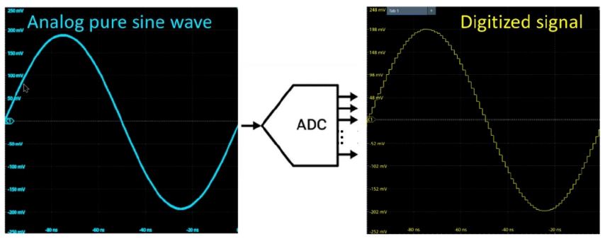
In the realm of high-frequency electronic measurements, oscilloscopes serve as the primary interface between analog phenomena and digital analysis. The quality of this analog-to-digital conversion fundamentally determines measurement accuracy, dynamic range, and signal fidelity. While traditional ADC specifications focus on theoretical bit resolution (K), where quantization occurs across 2^K discrete levels, real-world performance requires a more nuanced understanding of effective resolution.
ENOB emerges as the definitive metric for characterizing actual ADC performance, representing the number of bits that contribute meaningful information to the measurement process. For instance, while a 12-bit ADC theoretically provides 4,096 quantization levels, real-world implementations typically achieve ENOB values between 10.5 and 11.5 bits, corresponding to effective resolutions of approximately 1,500 to 3,000 meaningful levels.
Theoretical Foundation: The Relationship Between SNR and ENOB
The mathematical relationship between ENOB and Signal-to-Noise-and-Distortion Ratio (SINAD) forms the cornerstone of ADC performance analysis. According to IEEE Standard 1241-2010, ENOB can be expressed as:
ENOB = (SINAD – 1.76) / 6.02
Where SINAD represents the power ratio of signal to noise plus distortion, expressed in decibels. This relationship assumes sinusoidal input signals and establishes the fundamental limit that each additional effective bit corresponds to approximately 6.02 dB of SINAD improvement.
The theoretical maximum SINAD for an ideal K-bit ADC equals 6.02K + 1.76 dB, where the 1.76 dB term accounts for quantization noise characteristics in sinusoidal signals. However, practical implementations fall significantly short of this theoretical limit due to various system impairments.
System-Level Factors Affecting ENOB Performance
1. ADC Module Limitations
Modern high-speed ADCs exhibit several non-ideal characteristics that directly impact ENOB performance:
Quantization Noise: Even ideal ADCs introduce quantization noise with an RMS value of LSB/√12, where LSB represents the least significant bit voltage. This fundamental noise floor establishes the theoretical ENOB limit.
Differential Nonlinearity (DNL): Variations in quantization step sizes introduce distortion components that reduce effective resolution. DNL specifications typically range from ±0.5 to ±1.0 LSB in high-performance ADCs.
Integral Nonlinearity (INL): Systematic deviations from the ideal transfer function create harmonic distortion, particularly problematic for high-frequency signals where linearity requirements become increasingly stringent.
Aperture Jitter: Timing variations in the sampling process introduce noise that scales proportionally with input signal frequency and amplitude, making ENOB inherently frequency-dependent.
2. Front-End Signal Conditioning Impairments
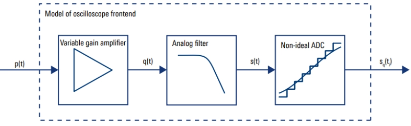
The oscilloscope’s analog front-end significantly influences overall ENOB performance through several mechanisms:
Variable Gain Amplifier (VGA) Characteristics: VGAs provide the dynamic range adjustment necessary for optimal ADC utilization but introduce frequency-dependent nonlinearities, particularly at higher gain settings. Typical VGA implementations exhibit third-order intercept points (IP3) ranging from +20 to +35 dBm, limiting large-signal linearity.
Anti-Aliasing Filter Performance: Analog low-pass filters prevent aliasing but introduce group delay variations, amplitude ripple, and phase nonlinearity that degrade signal fidelity. The trade-off between filter sharpness and phase response directly impacts ENOB, particularly for broadband signals.
Input Protection and ESD Circuits: Necessary protection elements introduce parasitic capacitances and nonlinear junction effects that become increasingly problematic at higher frequencies.
3. Thermal and Environmental Effects
Temperature variations affect component characteristics throughout the signal path:
ADC Temperature Drift: Reference voltage variations, comparator offset drift, and timing variations all contribute to temperature-dependent ENOB degradation.
Front-End Component Drift: VGA gain variations, filter characteristic changes, and impedance matching variations introduce measurement uncertainties that manifest as effective ENOB reduction.
Frequency-Dependent ENOB Characteristics
ENOB performance exhibits strong frequency dependence due to several physical phenomena:
Bandwidth Limitations: As signal frequencies approach the oscilloscope’s analog bandwidth, various parasitic effects become dominant, including:
Skin effect losses in conductors
Dielectric losses in substrates and interconnects
Parasitic reactances that affect impedance matching
Sampling Clock Jitter: The relationship between jitter-induced SNR degradation and frequency follows: SNR_jitter = -20·log₁₀(2π·f·σ_jitter)
Where f represents signal frequency and σ_jitter represents RMS jitter. This relationship explains why ENOB typically decreases by 6 dB per octave increase in frequency.
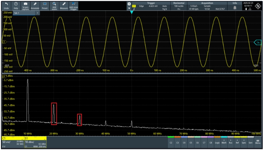
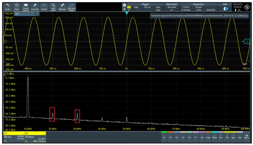
Harmonic Distortion Mechanisms: High-frequency signals exacerbate nonlinear effects in active components, generating harmonic and intermodulation products that directly reduce SINAD.
Measurement Methodology and Challenges
Signal Source Requirements
Accurate ENOB characterization demands signal sources with substantially better spectral purity than the device under test. Key requirements include:
Total Harmonic Distortion (THD): The source THD should be at least 10 dB better than the expected oscilloscope performance. For oscilloscopes with 60 dB SINAD, sources with THD < -70 dB become necessary.
Phase Noise Performance: Low phase noise ensures that jitter contributions from the source don’t dominate the measurement. Typical requirements specify phase noise < -130 dBc/Hz at 1 kHz offset for precision ENOB measurements.
Amplitude Stability: Long-term amplitude variations should remain within ±0.1 dB to ensure measurement repeatability.
Configuration Dependencies
ENOB measurements exhibit sensitivity to numerous oscilloscope settings:
Input Coupling Configuration: 50Ω vs. 1MΩ input impedance selection affects front-end noise figures and linearity characteristics. The 50Ω path typically provides better ENOB performance due to optimized impedance matching and reduced parasitic effects.
Vertical Sensitivity Optimization: ENOB generally improves when input signals approach full-scale deflection, maximizing SNR. However, overdrive conditions must be avoided to prevent compression-induced distortion.
Bandwidth Limitation Settings: Engaging bandwidth limit filters reduces high-frequency noise at the expense of signal rise time. The optimal setting depends on the specific measurement application and signal characteristics.
Averaging and Acquisition Parameters: Sample rate selection, record length, and averaging modes all influence measured ENOB values through their effects on noise floor and spectral resolution.
Practical Implications for Measurement Applications
Dynamic Range Considerations
ENOB directly determines the oscilloscope’s ability to resolve small signals in the presence of larger ones. For applications requiring wide dynamic range measurements:
Spurious-Free Dynamic Range (SFDR): ENOB establishes the theoretical limit for SFDR according to: SFDR ≈ 6.02·ENOB + 1.76 dB
Noise Floor Limitations: The effective noise floor equals full-scale range divided by 2^ENOB, establishing minimum detectable signal levels.
Signal Integrity Analysis
For high-speed digital applications, ENOB performance directly impacts:
Eye Diagram Measurements: Reduced ENOB manifests as increased noise in eye diagrams, potentially masking real jitter and noise contributions.
Jitter Analysis Accuracy: Phase noise measurements require high ENOB to distinguish between real jitter and measurement noise, particularly for low-jitter clock sources.
Power Supply Ripple Measurements: PSRR analysis demands high ENOB to characterize small ripple signals in the presence of DC bias levels.
Industry Perspectives and Best Practices
Specification Interpretation
When evaluating oscilloscope ENOB specifications, engineers should consider:
Test Conditions: ENOB values are meaningful only when accompanied by complete test condition specifications, including frequency, amplitude, and configuration settings.
Frequency Response Characterization: Single-point ENOB specifications provide limited insight; frequency-dependent ENOB curves offer more comprehensive performance assessment.
Application-Specific Requirements: Different measurement applications prioritize different aspects of ENOB performance, requiring careful specification analysis.
Optimization Strategies
To maximize ENOB performance in practical applications:
Signal Level Optimization: Utilize maximum available input range without causing compression or clipping.
Bandwidth Matching: Select minimum bandwidth adequate for signal characteristics to minimize noise contributions.
Time-Interleaved Architectures: Multi-channel ADC implementations enable higher sample rates while maintaining resolution, though calibration complexity increases significantly.
Hybrid ADC Designs: Combinations of flash, SAR, and delta-sigma architectures optimize performance for specific frequency ranges and resolution requirements.
Digital Correction Techniques: Advanced digital signal processing enables real-time correction of ADC nonlinearities, potentially improving ENOB by 1-2 bits.
System Integration Advances
Monolithic Integration: System-on-chip implementations reduce parasitic effects and improve matching between signal path components.
Advanced Packaging Technologies: 3D integration and advanced substrate technologies minimize interconnect-induced degradation.
AI-Enhanced Calibration: Machine learning algorithms enable adaptive calibration and compensation for temperature, aging, and process variations.
Conclusion
ENOB represents a comprehensive metric that encapsulates the complex interplay of factors affecting oscilloscope measurement quality. Unlike simple bit resolution specifications, ENOB reflects real-world performance limitations arising from ADC impairments, front-end nonlinearities, environmental effects, and system-level interactions.
Understanding ENOB’s frequency dependence, measurement challenges, and practical implications enables engineers to make informed decisions regarding oscilloscope selection and optimization. As measurement requirements continue to evolve toward higher frequencies, greater dynamic range, and improved precision, ENOB will remain the definitive metric for characterizing analog-to-digital conversion quality in high-performance oscilloscopes.
The future of oscilloscope technology lies in addressing the fundamental limitations that constrain ENOB performance through advanced ADC architectures, improved system integration, and intelligent calibration techniques. By maintaining focus on these system-level performance metrics, the industry can continue advancing measurement capabilities to meet the demands of next-generation electronic systems.
In the realm of electronic circuit design, one of the most fundamental challenges engineers face is converting the raw output of rectifier circuits into usable power for electronic devices. The output voltage from a typical rectifier circuit presents as a unidirectional pulsating DC voltage—a form that, while maintaining consistent polarity, exhibits significant amplitude fluctuations that render it unsuitable for direct use in sensitive electronic circuits. This comprehensive guide explores the critical role of filter circuits in transforming this pulsating voltage into the smooth, stable DC power that modern electronics demand.
Filter circuits represent a cornerstone technology in power supply design, employing components with specific impedance characteristics to selectively remove unwanted AC components while preserving the essential DC voltage. Through careful analysis of capacitors, inductors, and active components, engineers can design filtering solutions that meet the stringent requirements of today’s electronic systems.
Understanding the Need for Filtering
The Nature of Pulsating DC Voltage
The output from rectifier circuits, while unidirectional, carries inherent limitations that make it incompatible with most electronic applications. This pulsating DC voltage maintains a consistent polarity throughout its cycle but experiences significant amplitude variations over time, creating a waveform characterized by periodic fluctuations. These variations, if left unfiltered, can cause erratic behavior in electronic circuits, leading to noise, instability, and potential component damage.
From a theoretical perspective, this pulsating waveform can be understood through waveform decomposition principles. The complex pulsating signal can be mathematically broken down into two distinct components: a stable DC component representing the average voltage level, and a series of AC components with varying frequencies that correspond to the unwanted ripple. The DC component carries the useful power that electronic circuits require, while the AC components represent noise that must be eliminated through effective filtering.
Fundamental Filtering Principles
The success of any filter circuit relies on exploiting the distinct impedance characteristics that different components exhibit when faced with AC versus DC signals. This selective impedance behavior forms the foundation of all filtering techniques, allowing engineers to create circuits that preferentially pass desired signals while attenuating unwanted components.
Capacitors demonstrate this principle through their fundamental electrical property often described as “block DC, pass AC.” When subjected to DC voltage, a capacitor charges to the applied voltage and then acts as an open circuit, preventing further current flow. Conversely, AC signals encounter a reactance that decreases with increasing frequency, allowing high-frequency noise components to pass through with minimal impedance. This dual behavior, combined with the capacitor’s energy storage capability, makes it an ideal component for filtering applications.
Inductors exhibit the complementary behavior, often characterized as “block AC, pass DC.” For DC applications, an ideal inductor presents zero resistance, allowing steady current to flow unimpeded. However, when faced with AC signals, inductors generate an inductive reactance that increases with frequency, effectively blocking high-frequency components while allowing the DC component to pass through unchanged.
Basic Filter Circuit Configurations
Capacitor Filter Circuits
The most fundamental filtering approach employs a single capacitor connected in parallel with the load circuit. This simple yet effective configuration takes advantage of the capacitor’s ability to store energy during peak voltage periods and release it during voltage dips, thereby smoothing the overall output waveform.
In practical implementation, the capacitor charges rapidly during the peak portions of the pulsating input voltage. As the input voltage begins to decrease, the charged capacitor maintains the load voltage by discharging through the circuit. This charge-discharge cycle continues throughout the operation, with the capacitor acting as a reservoir that supplies current to the load when the input voltage is insufficient.
The effectiveness of capacitor filtering directly correlates with the capacitance value employed. Larger capacitance values store more energy, allowing them to maintain load voltage for longer periods between input peaks. This extended energy storage capability results in reduced voltage ripple and improved filtering performance. However, engineers must balance filtering effectiveness against practical considerations such as component size, cost, and initial charging current requirements.
Inductor Filter Circuits
Inductor-based filtering approaches the problem from a different perspective, utilizing the inductor’s high impedance to AC signals while maintaining minimal resistance to DC current. When positioned in series with the load circuit, an inductor acts as a frequency-selective impedance element that preferentially blocks AC components while allowing DC to pass with minimal voltage drop.
The filtering effectiveness of an inductor increases with inductance value, as higher inductance creates greater opposition to AC signals. However, this increased filtering capability comes with trade-offs, particularly in terms of DC resistance and physical size. Real inductors possess inherent resistance that causes voltage drops across the component, reducing the available output voltage. Additionally, larger inductance values typically require physically larger components, impacting circuit design constraints.
Advanced Filter Configurations
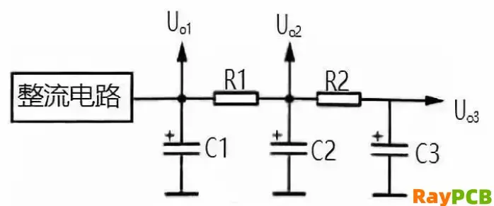
π-Type RC Filter Circuits
The π-type RC filter represents a significant advancement in filtering technology, combining multiple capacitors and resistors in a configuration that resembles the Greek letter π. This sophisticated approach provides superior filtering performance through a multi-stage attenuation process that systematically removes AC components while preserving DC voltage.
The circuit typically begins with a large input capacitor that provides initial filtering of the rectified voltage, removing the majority of low-frequency ripple components. The filtered signal then encounters a series resistance that works in conjunction with a second capacitor to create an additional filtering stage. This RC combination acts as a low-pass filter, further attenuating any remaining AC components that survived the initial filtering stage.
The design of π-type RC filters requires careful consideration of component values to achieve optimal performance. The input capacitor must be sized appropriately to provide adequate initial filtering without creating excessive inrush current that could damage rectifier diodes. The series resistance value represents a critical design parameter—insufficient resistance provides inadequate filtering, while excessive resistance causes significant DC voltage drops that reduce output voltage.
Multiple output taps can be implemented along the filter chain, providing various voltage levels with different degrees of filtering. Early taps in the circuit provide higher voltage levels with moderate filtering, while later stages offer lower voltages with superior ripple rejection. This flexibility allows a single filter circuit to serve multiple circuit requirements with varying noise tolerance levels.
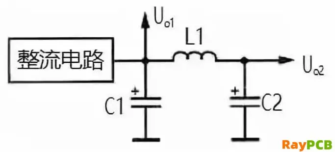
π-Type LC Filter Circuits
The π-type LC filter configuration replaces the series resistor with an inductor, creating a more efficient filtering system that maintains excellent AC rejection while minimizing DC voltage losses. This substitution leverages the inductor’s ability to present high impedance to AC signals while maintaining minimal resistance to DC current.
The advantages of LC filtering become particularly apparent in high-current applications where resistive voltage drops would be prohibitive. Unlike resistors, which dissipate power as heat regardless of current type, inductors provide frequency-selective impedance that targets only the unwanted AC components. This selective behavior allows LC filters to achieve superior filtering performance while maintaining higher efficiency and better voltage regulation.
The implementation of π-type LC filters requires attention to inductor specifications and behavior. Real inductors possess both inductance and resistance characteristics, with the resistive component contributing to voltage drops and power losses. High-quality filter inductors minimize this resistance while maximizing inductance, though such components typically involve higher costs and larger physical dimensions.
Active Electronic Filter Circuits
Basic Electronic Filter Implementation
Electronic filter circuits represent an evolution in filtering technology, incorporating active components such as transistors to enhance traditional passive filtering approaches. The basic electronic filter employs a transistor as an active filtering element, with its base circuit connected to an RC filter network that provides the filtering reference.
The transistor in this configuration functions as a voltage follower with current amplification capabilities. The RC network at the transistor’s base provides a filtered reference voltage, while the transistor’s emitter follows this voltage with the ability to supply significantly higher current to the load. This arrangement creates an equivalent capacitance effect that far exceeds the physical capacitor value, as the effective filtering capacitance becomes the product of the physical capacitor and the transistor’s current gain.
This amplification effect allows electronic filters to achieve superior filtering performance with smaller physical capacitors, addressing space and cost constraints common in modern electronic design. The transistor’s current gain effectively multiplies the filtering capacitor’s value, creating the electrical equivalent of a much larger capacitor without the associated physical bulk.
Electronic Regulator Filter Circuits
Advanced electronic filter designs incorporate voltage regulation components such as Zener diodes to provide both filtering and voltage stabilization in a single circuit. This combined approach addresses two critical power supply requirements simultaneously, creating systems that provide both clean and stable output voltage.
The Zener diode in these circuits establishes a stable reference voltage at the transistor’s base, ensuring consistent output voltage regardless of input variations or load changes. The series resistance limits current through the Zener diode while maintaining proper bias conditions for both regulation and filtering operations.
Compound transistor configurations can further enhance electronic filter performance, using multiple transistors in Darlington or similar arrangements to achieve even higher current gains. These advanced configurations multiply the effective filtering capacitance by the product of individual transistor gains, creating extremely effective filtering with minimal component requirements.
Design Considerations and Optimization
Component Selection Strategies
Successful filter circuit design requires careful attention to component specifications and their interaction within the complete system. Capacitor selection must consider not only capacitance value but also voltage rating, temperature coefficient, and ESR characteristics. Low ESR capacitors provide superior high-frequency filtering performance, while adequate voltage ratings ensure reliable operation under all circuit conditions.
Inductor selection involves balancing inductance value, DC resistance, current handling capability, and physical constraints. High-quality filter inductors feature low DC resistance to minimize voltage drops while providing adequate inductance for effective filtering. Core material selection affects both performance and cost, with ferrite cores offering good performance for most applications while more exotic materials may be required for demanding specifications.
Performance Optimization Techniques
Filter circuit optimization involves systematic analysis of ripple reduction requirements, voltage regulation needs, and efficiency considerations. Mathematical modeling can predict filter performance and guide component selection, while simulation tools allow verification of design approaches before physical implementation.
Load regulation characteristics must be considered throughout the design process, as filter circuit behavior can vary significantly with changing load conditions. Some filter configurations maintain consistent performance across wide load ranges, while others may require additional regulation circuitry for optimal performance.
Conclusion
Filter circuits represent an essential technology in modern electronics, enabling the conversion of raw rectified power into the clean, stable DC voltage that electronic systems require. Through understanding of fundamental filtering principles and careful application of various circuit configurations, engineers can design power supply systems that meet the demanding requirements of contemporary electronic applications.
The evolution from simple capacitor filters through advanced electronic filtering techniques demonstrates the continuous advancement in power supply technology. Each configuration offers distinct advantages and limitations, requiring engineers to carefully match filtering approaches to specific application requirements.
As electronic systems continue to demand higher performance and greater efficiency, filter circuit design remains a critical skill for electronics engineers. Mastery of these fundamental principles provides the foundation for tackling increasingly sophisticated power supply challenges in next-generation electronic systems.
Converting direct current (DC) from batteries or solar panels into alternating current (AC) for household appliances is a fundamental requirement in many electrical projects. A DC to AC inverter circuit transforms 12V DC input into 220V AC output, enabling you to power standard household devices from battery sources. This comprehensive guide will walk you through the theory, components, design considerations, and step-by-step construction of a reliable 12V to 220V inverter circuit.
Understanding Inverter Fundamentals
An inverter circuit performs the essential function of converting DC voltage into AC voltage through electronic switching. The basic principle involves rapidly switching the DC input on and off to create a square wave output, which can then be filtered and transformed to approximate a sine wave. The switching frequency typically ranges from 50Hz to 60Hz to match standard AC power frequencies.
The conversion process requires several key stages: oscillation generation, power switching, voltage transformation, and output filtering. Modern inverter designs often incorporate pulse width modulation (PWM) techniques to improve output waveform quality and reduce harmonic distortion. Understanding these fundamentals helps in selecting appropriate components and designing efficient circuits.
Essential Components and Their Functions
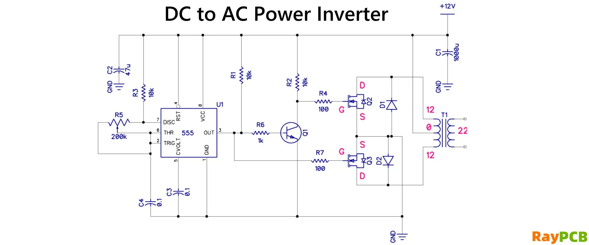
The heart of any inverter circuit lies in its carefully selected components. The primary oscillator can be built using the popular CD4047 CMOS integrated circuit, which generates stable square wave signals at the required frequency. This IC provides complementary outputs that drive the power switching stage with precise timing control.
Power MOSFETs serve as the main switching elements, handling the heavy current loads while maintaining high efficiency. IRF540 or similar N-channel MOSFETs are commonly used due to their low on-resistance and high current handling capability. These transistors must be mounted on adequate heat sinks to dissipate the generated heat during switching operations.
The step-up transformer represents a critical component that boosts the 12V DC (converted to AC) up to 220V AC output. A center-tapped transformer with appropriate turns ratio is essential, typically requiring a 12-0-12V primary winding and a 220V secondary winding. The transformer rating should match or exceed the intended output power requirements.
Supporting components include gate driver circuits for proper MOSFET switching, protection diodes, filtering capacitors, and current limiting resistors. Each component plays a vital role in ensuring stable operation and protecting the circuit from damage due to overcurrent or voltage spikes.
Circuit Design and Topology
The most common topology for simple inverter circuits is the push-pull configuration using a center-tapped transformer. This design alternately switches current through each half of the primary winding, creating an alternating magnetic field that induces AC voltage in the secondary winding.
The CD4047 oscillator generates two complementary square wave signals, each driving one MOSFET in the push-pull arrangement. The frequency is determined by external timing components, typically a resistor and capacitor combination. Careful calculation of these values ensures accurate 50Hz or 60Hz output frequency.
Gate drive circuits may be necessary to provide sufficient current to rapidly switch the power MOSFETs. Simple resistor networks can work for low-power applications, but dedicated gate driver ICs like IR2110 provide better performance for higher power inverters. Proper gate driving reduces switching losses and improves overall efficiency.
Output filtering helps smooth the square wave output into a more sinusoidal waveform. Simple LC filters consisting of inductors and capacitors can significantly improve the output waveform quality, reducing harmonic content that might interfere with sensitive electronic devices.
Step-by-Step Construction Process
Begin construction by preparing a suitable PCB or stripboard layout that accommodates all components with proper spacing for heat dissipation. The layout should minimize trace resistance for high-current paths while maintaining adequate isolation between high and low voltage sections.
Start by installing and testing the oscillator section using the CD4047 IC along with its timing components. Verify that the IC produces complementary square wave outputs at the desired frequency using an oscilloscope or frequency meter. Adjust timing components if necessary to achieve precise frequency control.
Next, install the power MOSFET switches along with their heat sinks and gate drive circuits. Use appropriate wire gauges for high-current connections, typically 12 AWG or larger for the primary circuit. Ensure all connections are secure and properly insulated to prevent short circuits.
Mount the step-up transformer securely and connect the center-tapped primary to the MOSFET switches. The secondary winding connects to the output terminals through appropriate filtering components. Double-check all wiring against the schematic before applying power to prevent component damage.
Testing and Troubleshooting
Initial testing should begin with reduced input voltage and no load connected. Use a digital multimeter to verify proper DC voltages at various test points throughout the circuit. Check that the oscillator produces stable square wave outputs and that MOSFETs switch properly.
Gradually increase input voltage while monitoring component temperatures, particularly the MOSFETs and transformer. Any excessive heating indicates problems that must be resolved before proceeding. Common issues include improper gate drive signals, inadequate heat sinking, or transformer saturation.
Connect a small resistive load such as an incandescent bulb to test output performance. Measure output voltage and frequency under load conditions, adjusting timing components if necessary. The output should remain stable across reasonable load variations.
Advanced testing involves examining output waveform quality using an oscilloscope. Pure square wave outputs will show significant harmonic content, while filtered outputs should approximate sine waves with reduced distortion. Frequency spectrum analysis can reveal harmonic levels for compliance with power quality standards.
Safety Considerations and Precautions
Working with inverter circuits involves potentially dangerous voltages and currents that demand strict safety protocols. Always disconnect input power before making circuit modifications and use appropriate personal protective equipment when testing high voltage outputs.
Proper grounding and isolation are essential for safe operation. The output AC voltage should be properly grounded through appropriate earth connections, and the circuit enclosure must provide adequate protection against accidental contact with live components.
Overcurrent protection through fuses or circuit breakers prevents damage from short circuits or overload conditions. These protective devices should be rated appropriately for the expected operating currents with sufficient margin for safety.
Heat dissipation requires careful attention to prevent component failure and fire hazards. Adequate ventilation, proper heat sink sizing, and temperature monitoring help ensure safe operation under all load conditions.
Performance Optimization and Efficiency
Inverter efficiency depends heavily on component selection and circuit design. Using MOSFETs with low on-resistance reduces conduction losses, while minimizing switching times reduces switching losses. Proper gate drive circuits ensure fast, clean switching transitions.
Transformer selection significantly impacts overall efficiency and regulation. High-quality transformers with low core losses and appropriate wire gauges minimize power dissipation. Core materials and construction techniques affect both efficiency and electromagnetic interference generation.
Output filtering improves waveform quality but adds some power loss. Balancing filter effectiveness against efficiency requires careful component selection and circuit optimization. Active filtering techniques can provide better performance than passive approaches in some applications.
Applications and Practical Uses
Simple 12V to 220V inverters find widespread use in automotive applications, solar power systems, emergency backup power, and portable power solutions. Understanding load characteristics helps determine appropriate inverter specifications and ensures reliable operation.
Resistive loads such as incandescent bulbs and heating elements are easiest to handle, requiring only appropriate power ratings. Inductive loads like motors and transformers present greater challenges due to startup currents and reactive power requirements.
Electronic loads including computers and sensitive equipment may require high-quality sine wave outputs with low harmonic distortion. Modified sine wave inverters work with many devices but can cause problems with some electronic equipment.
This fundamental inverter design provides an excellent foundation for understanding power conversion principles while delivering practical utility for numerous applications. Proper construction, testing, and safety practices ensure reliable performance and safe operation in demanding environments.
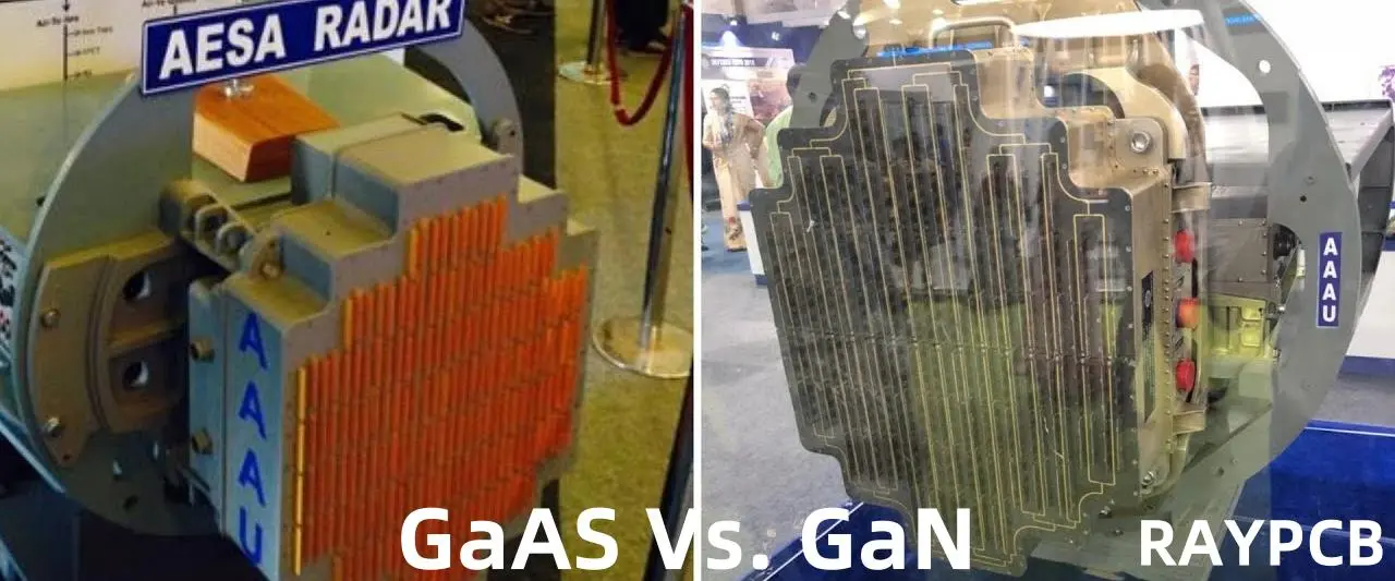
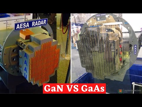
The radar technology landscape has undergone significant transformation in recent years, with two prominent technologies leading the charge: Gallium Arsenide (GaAs) and Gallium Nitride (GaN) radar systems. Understanding the fundamental differences between GAA (GaAs) and GaN radar technologies is crucial for engineers, procurement specialists, and decision-makers in defense, automotive, aerospace, and telecommunications industries.
Modern radar applications demand higher performance, improved efficiency, and enhanced reliability. As traditional silicon-based technologies reach their physical limitations, compound semiconductors like GaAs and GaN have emerged as superior alternatives, each offering unique advantages for specific applications. This comprehensive analysis explores the technical specifications, performance characteristics, cost implications, and practical applications of both technologies.
The choice between GAA and GaN radar systems significantly impacts system performance, operational costs, and long-term viability. While both technologies utilize gallium-based compounds, their distinct material properties result in vastly different capabilities and use cases. This article provides an in-depth comparison to help stakeholders make informed decisions based on their specific requirements.
Gallium Nitride (GaN) radar represents the cutting-edge of semiconductor technology in radar applications. GaN is a wide-bandgap semiconductor material that offers exceptional performance characteristics, making it ideal for high-power, high-frequency radar systems. The technology has revolutionized radar capabilities across military, commercial, and civilian applications.
GaN radar systems utilize the unique properties of gallium nitride semiconductors to achieve superior power density, efficiency, and frequency response compared to traditional technologies. The wide bandgap of GaN (approximately 3.4 eV) enables operation at higher voltages, temperatures, and frequencies while maintaining excellent efficiency and reliability.
Key Characteristics of GaN Radar
The fundamental properties of GaN make it exceptionally suitable for radar applications. The material exhibits high electron mobility, excellent thermal conductivity, and remarkable stability under extreme operating conditions. These characteristics translate into radar systems that can operate at higher power levels while maintaining consistent performance across varying environmental conditions.
GaN radar systems typically operate efficiently at frequencies ranging from L-band to Ka-band and beyond, making them versatile solutions for diverse applications. The technology’s ability to handle high power densities enables compact system designs without compromising performance, a critical advantage in space-constrained applications.
Performance Advantages of GaN Radar
GaN radar technology offers several performance advantages that make it attractive for demanding applications. The high power density capability allows for more compact antenna designs and reduced system size while maintaining or improving radar range and resolution. This is particularly valuable in airborne and space-based applications where size and weight constraints are critical.
The efficiency of GaN radar systems typically exceeds 50%, significantly higher than older technologies. This improved efficiency translates into reduced power consumption, lower heat generation, and enhanced system reliability. The reduced thermal load also simplifies cooling requirements, further contributing to system compactness and reliability.
GaN radar systems demonstrate excellent linearity characteristics, enabling advanced waveform generation and processing techniques. This capability is essential for modern radar applications that require sophisticated signal processing, electronic warfare countermeasures, and multi-function operations.
Understanding GAA (GaAs) Radar Technology
What is GAA Radar?
Gallium Arsenide (GaAs) radar technology has been a cornerstone of high-performance radar systems for several decades. GaAs is a compound semiconductor that offers superior performance compared to silicon while remaining more cost-effective than newer wide-bandgap materials. The technology has been extensively developed and optimized for radar applications, resulting in mature, reliable solutions.
GaAs-based radar systems leverage the material’s excellent electron mobility and relatively wide bandgap (1.42 eV) to achieve good performance in microwave and millimeter-wave applications. The technology has been particularly successful in applications requiring moderate power levels and excellent noise performance.
Key Characteristics of GAA Radar
GaAs radar technology is characterized by excellent noise performance, making it ideal for sensitive receiver applications and low-noise amplification. The material’s electron mobility is superior to silicon, enabling high-frequency operation with good gain and efficiency characteristics.
The maturity of GaAs technology means that manufacturing processes are well-established, resulting in consistent quality and relatively predictable costs. This maturity also translates into extensive design experience and readily available component libraries, simplifying system development and integration.
Performance Characteristics of GAA Radar
GAA radar systems excel in applications requiring excellent noise figure performance and moderate power levels. The technology is particularly well-suited for receiver front-ends, low-noise amplifiers, and mixer circuits where noise performance is critical to overall system sensitivity.
GaAs radar systems typically operate efficiently in the microwave frequency range, with good performance extending into millimeter-wave bands. While power handling capability is more limited compared to GaN, GaAs systems offer excellent linearity and stability characteristics that make them suitable for precision radar applications.
The most significant difference between GAA and GaN radar technologies lies in their power handling capabilities and efficiency characteristics. GaN radar systems can handle significantly higher power densities, typically 5-10 times greater than GaAs systems. This advantage stems from GaN’s superior thermal conductivity and higher breakdown voltage.
GaN radar efficiency typically ranges from 50-65%, while GaAs systems generally achieve 25-40% efficiency. This efficiency difference has profound implications for system design, power consumption, and thermal management. Higher efficiency translates directly into reduced power supply requirements, simplified cooling systems, and improved system reliability.
The power advantage of GaN becomes particularly pronounced at higher frequencies. While both technologies can operate at millimeter-wave frequencies, GaN maintains its power and efficiency advantages even as frequency increases, making it the preferred choice for high-frequency, high-power applications.
Frequency Response and Bandwidth
Both GAA and GaN radar technologies offer excellent frequency response characteristics, but with different strengths. GaN radar systems maintain consistent performance across broader frequency ranges, making them suitable for wideband and multi-band applications. The technology’s inherent characteristics enable operation from L-band through Ka-band and beyond with minimal performance degradation.
GaAs radar systems traditionally excel in specific frequency bands where their noise performance advantages are most pronounced. The technology is particularly effective in applications requiring exceptional sensitivity and low-noise operation, even if maximum power output is not the primary concern.
The bandwidth capabilities of both technologies are sufficient for modern radar applications, including pulse compression, frequency agility, and spread spectrum techniques. However, GaN’s broader operating bandwidth provides greater flexibility for multi-function radar systems and software-defined radio applications.
Thermal Performance and Reliability
Thermal management represents a critical differentiator between GAA and GaN radar technologies. GaN’s superior thermal conductivity (approximately 1.3 W/cm·K) compared to GaAs (0.46 W/cm·K) enables better heat dissipation and improved thermal performance. This characteristic is crucial for high-power radar applications where thermal management directly impacts system reliability and performance.
GaN radar systems can operate at higher junction temperatures while maintaining stable performance, reducing cooling requirements and enabling more compact system designs. The improved thermal performance also contributes to longer component lifetimes and enhanced system reliability.
The reliability characteristics of both technologies are excellent when properly designed and implemented. However, GaN’s ability to operate at higher temperatures and power levels while maintaining performance provides additional margin for robust system operation in challenging environments.
Cost Considerations
Cost analysis between GAA and GaN radar technologies involves multiple factors beyond initial component prices. While GaAs components are generally less expensive per unit, the total system cost comparison must consider performance capabilities, power consumption, cooling requirements, and system complexity.
GaN radar systems, despite higher initial component costs, often provide better value in high-performance applications due to their superior efficiency and power handling capabilities. The reduced power consumption and simplified cooling requirements can offset higher component costs in many applications.
The cost differential between technologies continues to narrow as GaN manufacturing volumes increase and processes mature. For many applications, the performance advantages of GaN justify any cost premium, particularly when total cost of ownership is considered.
Military and defense radar applications represent one of the most demanding environments for radar technology, requiring high performance, reliability, and adaptability. Both GAA and GaN radar technologies serve important roles in this sector, but their applications often differ based on specific requirements.
GaN radar technology has become the preferred choice for high-power military radar applications, including long-range surveillance radars, fire control systems, and active electronically scanned arrays (AESAs). The technology’s high power density enables compact, lightweight radar systems suitable for airborne platforms, ships, and mobile ground systems.
The efficiency advantages of GaN radar are particularly valuable in military applications where power generation and consumption directly impact operational capabilities. Reduced power requirements translate into longer mission endurance, reduced fuel consumption, and simplified logistics support.
GAA radar technology continues to play important roles in military applications requiring exceptional sensitivity and noise performance. Applications such as electronic warfare systems, precision tracking radars, and communication systems often benefit from GaAs technology’s superior noise characteristics.
Commercial Aviation and Air Traffic Control
Commercial aviation and air traffic control applications present unique requirements for radar technology, emphasizing reliability, precision, and cost-effectiveness. Both GAA and GaN radar technologies serve important roles in this sector, with applications ranging from weather radar to collision avoidance systems.
GaN radar technology is increasingly adopted for weather radar applications where high power and wide bandwidth are essential for accurate precipitation detection and wind measurement. The technology’s efficiency advantages also reduce operating costs for airlines and airports through lower power consumption.
Air traffic control radar systems benefit from both technologies depending on specific requirements. Primary surveillance radars often utilize GaN technology for its power and range capabilities, while secondary surveillance radars may employ GaAs technology where sensitivity and cost are primary concerns.
The reliability requirements of commercial aviation favor both technologies when properly implemented, but the simplified thermal management of GaN systems provides advantages in challenging installation environments.
Automotive Radar Systems
The automotive industry represents one of the fastest-growing markets for radar technology, driven by autonomous driving capabilities and advanced driver assistance systems (ADAS). The unique requirements of automotive applications present interesting trade-offs between GAA and GaN radar technologies.
GaN radar technology offers advantages for long-range automotive radar applications, providing the power and efficiency needed for highway-speed collision avoidance and adaptive cruise control systems. The technology’s compact size and high integration capability align well with automotive packaging constraints.
Short-range automotive radar applications, such as parking assistance and blind-spot monitoring, may benefit from GaAs technology’s cost advantages and excellent noise performance. These applications typically operate at lower power levels where GaN’s power advantages are less critical.
The automotive industry’s emphasis on cost reduction and high-volume manufacturing favors mature technologies with established supply chains. However, the performance advantages of GaN technology are driving increased adoption as system requirements become more demanding.
Telecommunications and 5G Infrastructure
Telecommunications infrastructure, particularly 5G networks, presents unique requirements for radar-like technologies used in beamforming and massive MIMO applications. While not traditional radar applications, these systems share many technical requirements with radar systems.
GaN technology has become the preferred choice for 5G base station applications due to its efficiency and power handling capabilities. The technology enables compact, efficient amplifiers that reduce operating costs and simplify installation requirements.
The integration capabilities of both technologies are important for telecommunications applications where size and cost constraints are significant. GaN’s higher integration potential and reduced component count provide advantages in system-level implementations.
Performance Metrics and Benchmarking
Power Output and Efficiency Metrics
Quantitative comparison of power output and efficiency metrics reveals the significant advantages of GaN radar over GAA radar in high-power applications. Typical GaN radar amplifiers achieve power densities of 5-10 W/mm of gate periphery, compared to 1-2 W/mm for GaAs amplifiers at similar frequencies.
Efficiency measurements consistently favor GaN technology, with practical implementations achieving 50-65% power-added efficiency compared to 25-40% for GaAs systems. This efficiency advantage becomes more pronounced at higher frequencies and power levels, making GaN the clear choice for demanding applications.
The power output capability of GaN radar systems enables new system architectures and applications that were not practical with previous technologies. High-power, compact radar systems can now be implemented in space-constrained environments while maintaining excellent performance characteristics.
Noise Figure and Sensitivity Analysis
Noise figure performance represents an area where GAA radar technology traditionally maintains advantages over GaN radar systems. GaAs low-noise amplifiers typically achieve noise figures of 0.5-1.0 dB in the microwave frequency range, compared to 1.0-2.0 dB for comparable GaN amplifiers.
However, the noise figure advantage of GaAs must be considered in the context of overall system performance. The higher power output capability of GaN systems often enables system architectures that compensate for higher noise figures through increased transmitter power and improved antenna gain.
Recent developments in GaN technology have significantly reduced the noise figure gap, with advanced GaN devices achieving noise figures approaching GaAs performance levels. This improvement, combined with GaN’s other advantages, further strengthens its position in radar applications.
Reliability and Lifetime Comparisons
Reliability analysis of GAA vs GaN radar technologies requires consideration of both inherent material properties and practical implementation factors. Both technologies demonstrate excellent reliability when properly designed and operated within specified limits.
GaN radar technology’s ability to operate at higher temperatures and power levels while maintaining performance provides additional reliability margin. The reduced thermal stress on components contributes to extended operational lifetimes and improved mean time between failures (MTBF).
Accelerated life testing of both technologies under realistic operating conditions shows comparable reliability characteristics when systems are properly designed. However, GaN’s superior thermal performance provides advantages in challenging operating environments where thermal stress is a primary failure mechanism.
Manufacturing and Production Considerations
Fabrication Processes and Yield
The manufacturing processes for GAA and GaN radar technologies differ significantly, impacting cost, yield, and scalability. GaAs technology benefits from decades of process development and optimization, resulting in mature manufacturing processes with high yields and predictable quality.
GaN radar technology manufacturing has progressed rapidly but remains more challenging than GaAs production. The growth of high-quality GaN epitaxial layers requires precise control of multiple parameters, and device fabrication involves several complex process steps.
Yield considerations favor GaAs technology for high-volume, cost-sensitive applications. However, GaN manufacturing yields continue to improve as processes mature and production volumes increase. The performance advantages of GaN often justify lower yields in demanding applications.
Supply Chain and Availability
Supply chain considerations play important roles in technology selection for radar applications. GaAs technology benefits from an established, mature supply chain with multiple suppliers and standardized processes. This maturity provides supply security and competitive pricing for high-volume applications.
GaN radar technology supply chains are developing rapidly but remain more limited than GaAs alternatives. However, significant investments in GaN manufacturing capacity are expanding availability and reducing supply chain risks.
The strategic importance of GaN technology has led to substantial government and industry investments in manufacturing capability, particularly in North America, Europe, and Asia. These investments are rapidly improving GaN availability and reducing dependence on limited supply sources.
Quality Control and Testing
Quality control and testing requirements differ between GAA and GaN radar technologies due to their distinct characteristics and failure modes. Both technologies require comprehensive testing to ensure performance and reliability, but the specific test requirements vary.
GaN radar devices require careful attention to thermal characteristics and high-power operation during testing. The technology’s ability to handle high power levels necessitates specialized test equipment and procedures to verify performance under realistic operating conditions.
GaAs testing procedures are well-established and standardized across the industry. The maturity of the technology has led to comprehensive understanding of failure modes and appropriate test methodologies to ensure quality and reliability.
Economic analysis of GAA vs GaN radar technologies must consider multiple cost factors beyond initial component prices. While GaAs components typically cost less per unit, total system costs depend on performance requirements, system complexity, and operational considerations.
GaN radar systems often require higher initial investment due to component costs and potentially more complex system integration. However, these costs must be evaluated against the performance benefits and operational advantages that GaN technology provides.
The cost gap between technologies continues to narrow as GaN manufacturing scales up and processes mature. Volume production and competition among suppliers are driving down GaN costs while performance advantages remain constant or improve.
Total Cost of Ownership Analysis
Total cost of ownership (TCO) analysis reveals that GaN radar systems often provide superior economic value despite higher initial costs. The efficiency advantages of GaN technology translate directly into reduced operational costs through lower power consumption and simplified cooling requirements.
Maintenance and support costs may favor GaN systems due to their improved reliability and reduced thermal stress. Fewer component failures and longer operational lifetimes contribute to lower lifecycle costs in many applications.
The compact size and reduced complexity of GaN radar systems can also reduce installation and infrastructure costs. Simplified power distribution, cooling systems, and mechanical structures offset higher component costs in many installations.
Return on Investment Projections
Return on investment (ROI) analysis for GaN radar technology depends heavily on application requirements and operational factors. Applications requiring high performance, efficiency, or compact size typically show favorable ROI for GaN technology within 2-5 years.
The improving cost structure of GaN technology enhances ROI projections over time. As manufacturing scales up and costs decline, the economic advantages of GaN radar systems become more compelling across a broader range of applications.
Long-term ROI considerations must also account for technology evolution and obsolescence risks. GaN technology’s position as the leading-edge solution provides better protection against technological obsolescence compared to mature technologies.
Future Trends and Technological Evolution
Emerging GaN Radar Innovations
The future of GaN radar technology includes several promising developments that will further enhance its capabilities and expand its applications. Advanced device structures, including enhancement-mode devices and monolithic microwave integrated circuits (MMICs), are improving performance while reducing system complexity.
Integration advances are enabling complete radar front-ends on single GaN chips, dramatically reducing size, cost, and complexity. These integrated solutions maintain the performance advantages of GaN technology while approaching the cost structures traditionally associated with silicon-based solutions.
Packaging innovations are addressing thermal management challenges and enabling even higher power densities. Advanced thermal interface materials and three-dimensional packaging approaches are pushing the boundaries of what’s possible with GaN radar technology.
GAA Technology Roadmap
While GaN technology captures much attention, GaAs radar technology continues to evolve and find new applications. Advanced GaAs processes are improving noise performance and frequency capabilities, maintaining the technology’s relevance in specialized applications.
Integration developments in GaAs technology focus on system-on-chip solutions that combine multiple functions on single substrates. These developments help GaAs technology maintain cost competitiveness while leveraging its noise performance advantages.
Niche applications continue to drive GaAs technology development, particularly in areas where ultimate sensitivity is more important than power output. These applications ensure continued investment in GaAs technology advancement.
Market Predictions and Industry Outlook
Market analysis predicts continued growth for both GAA and GaN radar technologies, with GaN capturing an increasing share of high-performance applications. The expanding automotive radar market represents a significant growth opportunity for both technologies.
Defense spending on advanced radar systems favors GaN technology due to its performance advantages and strategic importance. Government investments in GaN manufacturing capability are expected to accelerate technology adoption and reduce costs.
The 5G infrastructure buildout and emerging 6G technologies create additional markets for GaN technology, although these applications differ from traditional radar uses. The synergy between telecommunications and radar applications benefits GaN technology development.
Technical Implementation Guidelines
System Design Considerations
Implementing GAA or GaN radar technology requires careful consideration of system-level requirements and constraints. The choice between technologies should be based on thorough analysis of performance requirements, cost constraints, and operational considerations.
GaN radar system design must account for the technology’s high power density and thermal characteristics. Proper thermal management is essential to realize GaN’s performance advantages while maintaining reliability. System designers must consider heat sinking, airflow, and component placement to optimize thermal performance.
Power supply design differs significantly between GAA and GaN radar systems due to their different efficiency characteristics and voltage requirements. GaN systems typically require higher supply voltages but consume less current, impacting power supply design and distribution systems.
Integration and Compatibility Issues
Integration considerations play important roles in technology selection and system design. Both GAA and GaN technologies can be integrated with digital signal processing and control systems, but the specific requirements and interfaces may differ.
Legacy system compatibility may favor GaAs technology in upgrade applications where existing infrastructure and interfaces must be maintained. However, the performance advantages of GaN technology often justify more extensive system modifications.
Test and measurement equipment compatibility must be considered when implementing either technology. High-power GaN systems may require specialized test equipment and procedures that differ from those used with GaAs systems.
Performance Optimization Strategies
Optimizing performance in GAA and GaN radar systems requires different approaches based on each technology’s characteristics. GaN systems benefit from optimization strategies that leverage high power density and efficiency, while GaAs systems may focus on noise optimization and linearity.
Bias point optimization differs significantly between technologies. GaN devices typically operate in different bias regimes compared to GaAs devices, requiring different optimization approaches to achieve optimal performance.
Matching network design and optimization represent critical aspects of both technologies but with different emphasis. GaN systems must handle higher power levels and wider bandwidths, while GaAs systems may prioritize noise matching and stability.
Conclusion and Recommendations
Summary of Key Differences
The comparison between GAA and GaN radar technologies reveals distinct advantages and applications for each technology. GaN radar systems excel in high-power, high-efficiency applications where performance is the primary concern. The technology’s superior power density, efficiency, and thermal characteristics make it ideal for demanding military, aerospace, and high-performance commercial applications.
GAA radar technology maintains advantages in cost-sensitive applications and those requiring exceptional noise performance. The maturity of GaAs technology provides supply chain security and predictable costs that remain attractive for many applications.
The choice between technologies should be based on comprehensive analysis of requirements, including performance specifications, cost constraints, and operational considerations. Both technologies will continue to serve important roles in the radar industry, with their applications determined by specific system requirements.
Decision-Making Framework
Selecting between GAA and GaN radar technologies requires systematic evaluation of multiple factors. Performance requirements represent the primary consideration, with GaN technology favored for high-power applications and GaAs for low-noise applications.
Cost analysis must consider total cost of ownership rather than just initial component costs. Applications with high operational costs or demanding size constraints often favor GaN technology despite higher initial investment.
Technical risk assessment should consider technology maturity, supply chain security, and long-term viability. GaAs technology offers lower technical risk for many applications, while GaN provides better future-proofing for performance-critical systems.
Future Outlook and Strategic Recommendations
The future of radar technology will see continued adoption of GaN technology in high-performance applications, driven by its superior capabilities and improving cost structure. Organizations should develop GaN expertise and supply relationships to prepare for this transition.
GAA technology will continue to serve important roles in cost-sensitive and noise-critical applications. Maintaining capabilities in both technologies provides flexibility to optimize solutions for specific requirements.
Investment in advanced radar technologies should consider both current needs and future requirements. The rapid evolution of radar applications, particularly in automotive and telecommunications sectors, creates opportunities for both technologies but with different emphasis.
Strategic planning should account for the convergence of radar and communication technologies, particularly in 5G and future wireless systems. This convergence favors technologies with broad bandwidth and high integration capabilities, generally favoring GaN solutions.
The geopolitical importance of semiconductor technology adds strategic considerations to technology selection. Supply chain security and domestic manufacturing capability are increasingly important factors in technology decisions, particularly for defense and critical infrastructure applications.
Organizations should develop comprehensive technology roadmaps that consider both GAA and GaN technologies while preparing for future innovations. The rapid pace of semiconductor development ensures that today’s decisions will impact competitiveness for years to come, making strategic technology selection more critical than ever.
Modern livestock management has evolved significantly with the integration of digital technologies, transforming traditional farming practices into sophisticated, data-driven operations. Among the most impactful innovations is the development of automated livestock counting systems integrated directly into fencing infrastructure. These systems represent a convergence of precision agriculture, Internet of Things (IoT) technology, and advanced sensor networks, all orchestrated through carefully designed printed circuit boards (PCBs) that serve as the technological backbone of smart fencing solutions.
The need for automated livestock counting has emerged from several critical challenges facing contemporary livestock operations. Manual counting methods are labor-intensive, prone to human error, and often impractical for large-scale operations or remote locations. Traditional counting systems struggle with accuracy in varying environmental conditions, while the economic pressures on agricultural operations demand more efficient resource utilization and real-time operational insights. Automated counting modules embedded within fencing systems address these challenges by providing continuous, accurate monitoring without requiring additional infrastructure or significant changes to existing farm layouts.
The integration of counting modules into fencing systems offers unique advantages over standalone monitoring solutions. Fencing represents existing infrastructure that livestock must interact with regularly, making it an ideal platform for sensor deployment. Animals naturally pass through fence gates, creating predictable monitoring points that eliminate the need for additional structural installations. This integration approach reduces deployment costs, minimizes visual impact on pastoral landscapes, and leverages the power infrastructure often already present in modern fencing systems.
The automated livestock counting module represents a sophisticated electronic system requiring careful consideration of multiple interconnected subsystems. The core architecture centers around a microcontroller unit (MCU) that coordinates sensor inputs, processes counting algorithms, manages data storage, and handles communication protocols. Modern implementations typically employ ARM Cortex-M series processors or similar low-power, high-performance microcontrollers capable of real-time processing while maintaining extended battery life in remote applications.
Sensor integration forms the cornerstone of accurate livestock counting, with multiple sensing modalities often employed to ensure reliability across diverse environmental conditions. Infrared break-beam sensors provide reliable detection for animals passing through defined spaces, while passive infrared (PIR) sensors detect heat signatures and movement patterns. Ultrasonic sensors offer distance measurement capabilities, enabling the system to distinguish between different animal sizes and identify multiple animals passing simultaneously. Advanced implementations incorporate computer vision modules with low-power image processors, enabling sophisticated animal recognition and behavioral analysis.
Power management represents a critical design consideration, particularly for remote fencing applications where grid power may be unavailable. The PCB design must accommodate multiple power sources, including solar panels, rechargeable battery systems, and potentially energy harvesting from animal movement or environmental sources. Power management integrated circuits (PMICs) regulate voltage levels, manage charging cycles, and implement power-saving modes to extend operational life between maintenance intervals.
Communication capabilities enable integration with broader farm management systems and remote monitoring platforms. Modern livestock counting modules incorporate multiple communication protocols, including Wi-Fi for local area networks, cellular connectivity for wide-area coverage, and low-power wide-area network (LPWAN) technologies such as LoRaWAN for extended range with minimal power consumption. Bluetooth Low Energy (BLE) provides local connectivity for configuration and maintenance operations.
PCB Design Considerations
The printed circuit board design for livestock counting modules must address unique challenges associated with outdoor agricultural environments. Environmental protection represents the primary design consideration, as these systems must operate reliably in conditions ranging from extreme temperatures to high humidity, dust exposure, and potential chemical contamination from agricultural processes. The PCB layout must minimize moisture ingress paths, incorporate appropriate conformal coatings, and ensure thermal management across wide temperature ranges.
Signal integrity becomes particularly crucial when dealing with sensitive analog sensor inputs and high-frequency digital communications. Proper ground plane design, controlled impedance routing, and electromagnetic interference (EMI) shielding protect sensitive circuits from the electrically noisy environment typical of agricultural settings. Power supply noise, generated by motor-driven equipment and variable frequency drives common in modern farming operations, requires careful filtering and isolation techniques implemented at the PCB level.
Component selection for livestock counting modules prioritizes reliability, environmental tolerance, and long-term availability. Industrial-grade components with extended temperature ranges, enhanced moisture resistance, and proven reliability in harsh environments form the foundation of robust designs. Automotive-qualified components often provide excellent alternatives, as they undergo rigorous environmental testing and offer long-term supply chain stability crucial for agricultural applications with extended service lives.
The mechanical design of the PCB must accommodate installation within fencing systems while providing access for maintenance and configuration. Modular connector systems enable field replacement of sensors or communication modules without complete system replacement. The form factor must fit within standard fence post dimensions or gate mechanisms while maintaining structural integrity under mechanical stress from animal contact or weather exposure.
Sensor Integration and Processing
Effective livestock counting requires sophisticated sensor fusion algorithms implemented on the PCB’s processing platform. Multiple sensor inputs must be correlated and processed in real-time to provide accurate count data while filtering false positives from environmental factors. The PCB design must provide adequate analog-to-digital conversion capabilities with sufficient resolution and sampling rates to capture rapid animal movements while maintaining low power consumption.
Digital signal processing (DSP) capabilities, either through dedicated DSP processors or MCUs with integrated DSP functionality, enable implementation of advanced filtering algorithms. These algorithms differentiate between livestock and other moving objects such as wildlife, farm equipment, or environmental factors like moving vegetation. Machine learning inference capabilities, increasingly available in embedded processors, enable adaptive counting algorithms that improve accuracy over time through pattern recognition and behavioral analysis.
Sensor calibration and self-diagnostic capabilities require PCB designs that support precision voltage references, temperature compensation, and automated testing routines. Built-in test (BIT) functionality enables remote diagnosis of sensor performance and early detection of component degradation before complete system failure. This predictive maintenance capability reduces operational downtime and extends system service life.
The timing precision required for accurate counting necessitates high-quality clock sources and careful attention to timing distribution across the PCB. Crystal oscillators with appropriate temperature stability and aging characteristics ensure consistent timing performance across the operational temperature range. Clock domain crossing techniques become important when interfacing sensors operating at different sampling rates or communication protocols with varying timing requirements.
Communication and Connectivity
Modern livestock counting systems must integrate seamlessly with existing farm management infrastructure and provide reliable data transmission to centralized monitoring systems. The PCB design must accommodate multiple communication interfaces while managing power consumption and maintaining reliability in challenging RF environments. Agricultural settings often present unique RF challenges, including interference from electrical equipment, metallic structures, and varying terrain that affects signal propagation.
Cellular connectivity provides the most robust solution for remote monitoring, but requires careful antenna design and power management to ensure reliable operation. The PCB must integrate cellular modem modules with appropriate power sequencing, SIM card interfaces, and antenna matching networks optimized for the specific frequency bands used in the deployment region. Backup communication methods, such as satellite connectivity for extremely remote locations, may require additional RF design considerations.
Local area networking capabilities enable integration with on-farm systems such as existing Wi-Fi networks or dedicated agricultural IoT networks. The PCB design must support multiple networking protocols while maintaining electromagnetic compatibility with other farm equipment. Edge computing capabilities allow local data processing and decision-making, reducing communication bandwidth requirements and improving system responsiveness.
Data security and encryption capabilities must be implemented at the hardware level to protect sensitive operational information. Secure boot processes, hardware security modules (HSMs), and encrypted communication protocols protect against unauthorized access and data tampering. These security features require dedicated processing capabilities and secure storage elements integrated into the PCB design.
Manufacturing and Assembly Considerations
The manufacturing of PCBs for livestock counting modules requires specialized processes and quality control measures appropriate for harsh environment applications. Surface mount technology (SMT) assembly processes must accommodate components with enhanced environmental ratings while maintaining high reliability standards. Solder joint reliability becomes critical for long-term operation in temperature cycling and vibration environments typical of agricultural applications.
Conformal coating application protects assembled PCBs from moisture, chemical exposure, and environmental contamination. The coating selection must balance protection levels with thermal dissipation requirements and component accessibility for potential repairs. Advanced coating materials such as parylene provide superior protection but require specialized application equipment and processes.
Quality assurance processes for agricultural electronics must address the unique failure modes associated with outdoor operation. Accelerated aging tests, thermal cycling, humidity exposure, and vibration testing validate design robustness before deployment. In-circuit testing (ICT) and functional testing procedures verify proper assembly and initial calibration of sensor systems.
Supply chain management for agricultural electronics requires consideration of component lifecycle and availability over extended product lifespans. Agricultural equipment typically operates for decades, necessitating component selection strategies that ensure long-term availability or provide clear obsolescence management pathways. Strategic component inventory management and supplier diversification protect against supply chain disruptions.
Environmental Protection and Reliability
Environmental protection strategies for livestock counting PCBs must address multiple simultaneous stressors typical of agricultural environments. Temperature extremes ranging from arctic conditions to desert heat require component derating and thermal management strategies. Humidity control through desiccants, vapor barriers, and drainage design prevents condensation and corrosion within enclosures.
Chemical resistance becomes important in environments where cleaning agents, pesticides, and animal waste products may contact electronic systems. Materials selection for PCB substrates, component packages, and protective coatings must consider chemical compatibility with anticipated exposure scenarios. Galvanic corrosion prevention requires careful consideration of dissimilar metal combinations and appropriate surface treatments.
Mechanical protection strategies address impact resistance, vibration immunity, and structural integrity under varying mechanical loads. Gate-mounted systems experience repetitive mechanical stress from opening and closing operations, while fence-mounted systems must withstand animal contact and weather-induced movement. Shock mounting, flexible interconnections, and robust mechanical design prevent stress-related failures.
Lightning protection and electrical transient suppression protect sensitive electronics from the high-energy transients common in outdoor agricultural environments. Surge protection devices, proper grounding strategies, and isolation techniques prevent damage from nearby lightning strikes or electrical equipment switching transients. These protection systems must be integrated into the PCB design without compromising normal operation or adding excessive cost.
Future Developments and Integration Opportunities
The evolution of automated livestock counting systems continues toward increased sophistication and integration with broader precision agriculture platforms. Artificial intelligence capabilities, enabled by increasingly powerful embedded processors, will provide enhanced animal recognition, behavioral analysis, and predictive insights. Machine learning algorithms will adapt to specific farm conditions and animal populations, improving accuracy and reducing false positives over time.
Integration with blockchain technology offers opportunities for secure, immutable livestock tracking and supply chain verification. PCB designs must accommodate the cryptographic processing requirements for blockchain participation while maintaining power efficiency and real-time performance. Smart contracts and automated compliance reporting capabilities will streamline regulatory compliance and enhance traceability throughout the livestock supply chain.
Advanced sensor technologies, including miniaturized radar systems, LiDAR sensors, and hyperspectral imaging, will provide enhanced monitoring capabilities. These technologies require sophisticated PCB designs with high-speed digital processing, precision analog circuits, and advanced power management. The integration of these sensors into existing fencing infrastructure will demand innovative mechanical and electrical design approaches.
Edge computing and fog computing architectures will enable distributed intelligence throughout livestock operations. PCB designs must support local processing capabilities while maintaining connectivity to cloud-based analytics platforms. This distributed approach reduces latency, improves system reliability, and enables autonomous operation during communication outages.
Conclusion
The development of automated livestock counting modules represents a significant advancement in precision agriculture technology, with PCB design and manufacturing playing a crucial role in system success. The unique requirements of agricultural environments demand sophisticated engineering approaches that balance performance, reliability, and cost-effectiveness. Successful implementations require careful consideration of environmental protection, power management, sensor integration, and communication capabilities, all orchestrated through well-designed printed circuit boards.
The integration of these systems into existing fencing infrastructure provides a cost-effective deployment strategy that leverages existing agricultural infrastructure while providing valuable operational insights. As technology continues to evolve, these systems will become increasingly sophisticated, providing enhanced analytics capabilities and integration with broader farm management platforms.
The future of automated livestock counting lies in the continued miniaturization of sensors, advancement of processing capabilities, and integration with artificial intelligence systems. PCB designers and manufacturers must continue to innovate in materials science, manufacturing processes, and design methodologies to meet the evolving demands of precision agriculture. The success of these systems will ultimately depend on their ability to provide reliable, accurate, and cost-effective solutions that enhance livestock management while withstanding the challenges of agricultural environments.
Introduction: The Cornerstone of Reliable Digital Logic
In the realm of programmable logic devices where reliability meets versatility, the XC2C32A-VQG44AMS stands as a distinguished solution from Xilinx (now AMD). This military and space-grade Complex Programmable Logic Device (CPLD) represents the pinnacle of rugged digital logic implementation, designed specifically for applications where failure is not an option. As technology continues to advance, the demand for compact, efficient, and radiation-tolerant logic solutions grows ever stronger in aerospace, defense, and other mission-critical sectors. The XC2C32A-VQG44AMS exemplifies Xilinx’s commitment to delivering programmable solutions that excel in the most challenging environments.
The XC2C32A-VQG44AMS belongs to Xilinx‘s renowned CoolRunner-II CPLD family, combining high performance with ultra-low power consumption. At its core, this device features 32 macrocells organized into eight Function Blocks, interconnected through a sophisticated low-power Advanced Interconnect Matrix (AIM). This architecture enables efficient signal routing while minimizing power consumption, a critical factor for space and military applications.
The device’s architecture is engineered with eight Function Blocks, each receiving inputs from the AIM. Within each Function Block resides a Product Term array configured as a 40 by 56 P-term Programmable Logic Array (PLA), feeding into 16 macrocells. These macrocells contain numerous configuration bits enabling either combinational or registered modes of operation. The registers can be configured as D or T flip-flops, or as D latches, with global reset/preset capabilities.
The XC2C32A-VQG44AMS is housed in a 44-pin VTQFP (Very Thin Quad Flat Pack) package, offering a compact footprint for space-constrained applications. With its 750 equivalent gates and operating frequency capabilities up to 323 MHz, this CPLD delivers substantial processing power in a small form factor.
The “AMS” suffix in the part number designates this device for Automotive, Military, and Space applications. This classification indicates enhanced testing, qualification, and reliability specifications compared to commercial or industrial variants. The device undergoes rigorous screening for radiation tolerance, including Total Ionizing Dose (TID) and Single Event Effect (SEE) characterization.
For aerospace and defense applications, reliability is paramount. The XC2C32A-VQG44AMS meets stringent requirements for operation in extreme environments, with an extended temperature range and enhanced resistance to electromagnetic interference. These qualities make it ideal for satellite systems, military avionics, missile guidance systems, and other high-reliability applications where standard commercial components would be inadequate.
Power Efficiency and I/O Capabilities
One of the most notable features of the XC2C32A-VQG44AMS is its exceptional power efficiency. The CoolRunner-II architecture employs standard CMOS methods to achieve remarkably low power consumption—a critical advantage for battery-powered and heat-sensitive applications. With a standby current of approximately 16μA and ultra-low dynamic power consumption of 28.8μW, this CPLD significantly outperforms many competing solutions.
The device offers flexibility in I/O interfaces through two distinct I/O banks, supporting various JEDEC I/O standards. This versatility enables seamless integration with systems operating at different voltage levels (3.3V, 2.5V, 1.8V, and even 1.5V with Schmitt-trigger inputs). The I/O banking feature simplifies voltage translation between different system components, eliminating the need for additional level-shifting components.
Output pin configurations offer numerous options including slew rate limiting, bus hold, pull-up capabilities, open drain functionality, and programmable grounds. These features provide designers with extensive flexibility when interfacing with various external components.
Programming and Integration
The XC2C32A-VQG44AMS supports industry-standard IEEE 1149.1/1532 Boundary-Scan (JTAG) interfaces for programming, prototyping, and testing. This compliance ensures compatibility with existing development tools and test equipment. Programming is typically accomplished using Xilinx’s development environment, historically ISE Design Suite for CoolRunner-II devices.
For space applications, the device’s In-System Programming (ISP) capabilities are particularly valuable, allowing for configuration updates even after deployment. This feature enables remote updates and fixes, a crucial advantage for inaccessible systems such as satellites or deep-space probes.
Applications in Mission-Critical Systems
The XC2C32A-VQG44AMS finds its purpose in numerous high-reliability applications:
Satellite Systems: From command and control logic to sensor interfaces, this CPLD provides configurable logic solutions with radiation tolerance suitable for orbital and deep-space missions.
Military Avionics: For aircraft electronics requiring certification to stringent military standards, this device offers guaranteed performance across extreme environmental conditions.
Missile Guidance Systems: Where size, weight, and power (SWaP) constraints meet demanding performance requirements, this CPLD delivers efficient logic implementation.
Medical Equipment: Though primarily targeting defense and aerospace, the device’s reliability makes it suitable for life-critical medical devices requiring fail-safe operation.
Industrial Control: In harsh industrial environments where temperatures fluctuate widely and electromagnetic interference is prevalent, this device provides stable, reliable operation.
Competitive Ranking and Market Position
When ranking the XC2C32A-VQG44AMS among similar devices, several factors merit consideration:
Performance Rating: 8.5/10 The device delivers excellent performance for its class, with speeds up to 323 MHz and predictable timing characteristics. While newer FPGA technologies offer higher absolute performance, the deterministic timing of this CPLD provides significant advantages in real-time applications.
Reliability Rating: 9.5/10 Few competing devices match the reliability specifications of the XC2C32A-VQG44AMS. Its military and space qualification, coupled with Xilinx’s established track record in high-reliability markets, places it among the elite in dependable programmable logic.
Power Efficiency Rating: 9.0/10 The CoolRunner-II architecture’s focus on power efficiency results in exceptionally low power consumption. This efficiency translates to reduced thermal management requirements and extended battery life in portable systems.
Integration Ease Rating: 8.0/10 With industry-standard programming interfaces and comprehensive development tool support, the device integrates smoothly into established workflows. However, the learning curve associated with CPLD architecture may present challenges for teams more familiar with microcontrollers or FPGAs.
Cost-Effectiveness Rating: 7.5/10 Military and space-grade components command premium pricing, and the XC2C32A-VQG44AMS is no exception. While expensive compared to commercial alternatives, its specific capabilities justify the investment for applications where failure is not an option.
Overall Rating: 8.7/10 The XC2C32A-VQG44AMS earns its position as a top-tier solution for mission-critical programmable logic applications. Its combination of reliability, performance, and power efficiency makes it an excellent choice for systems requiring the highest standards of dependability.
Conclusion
The XC2C32A-VQG44AMS represents a specialized pinnacle of programmable logic technology, tailored specifically for the most demanding applications in aerospace, defense, and other mission-critical sectors. While newer technologies continue to emerge, the unique combination of reliability, deterministic timing, and radiation tolerance ensures this device maintains its relevance in specialized applications where proven performance under extreme conditions takes precedence over cutting-edge features.
For system designers working on projects where failure is not an option, the XC2C32A-VQG44AMS provides a trusted foundation upon which to build dependable digital logic systems. Its continued use in critical infrastructure underscores the enduring value of well-engineered, purpose-built components in an increasingly disposable technological landscape.
In the world of electronics and signal processing, few components are as fundamental and widely used as the low pass filter. These essential circuit elements play a crucial role in countless applications, from the audio systems in your home theater to life-saving medical devices. A low pass filter, as the name suggests, allows low-frequency signals to pass through while attenuating (reducing) signals with frequencies higher than a designated cutoff point. This seemingly simple function is the backbone of modern electronic systems, helping engineers and designers achieve cleaner signals, reduce noise, and extract only the information they need.
Whether you’re an electronics hobbyist, a student, or a seasoned engineer, understanding low pass filters is essential for designing effective electronic systems. This comprehensive guide explores everything you need to know about low pass filters in 2025, from basic principles to advanced design techniques, real-world applications, and emerging trends. We’ll break down the various types, explain how to design them for your specific needs, and provide practical tips to avoid common pitfalls.
A low pass filter (LPF) is an electronic circuit designed to allow signals below a specific cutoff frequency to pass through while attenuating (reducing) signals above that frequency. This fundamental function makes it one of the most important components in signal processing and electronic design.
Basic Principles of Operation
The operation of a low pass filter is based on the frequency-dependent behavior of capacitors and inductors. In simple terms, capacitors present high impedance (resistance) to low-frequency signals and low impedance to high-frequency signals. Inductors do the opposite, offering low impedance to lower frequencies and high impedance to higher frequencies. By strategically combining these components with resistors, engineers can create circuits that discriminate between signals based on their frequency content.
When a complex signal (containing multiple frequencies) enters a low pass filter, the circuit allows the low-frequency components to pass through relatively unchanged while progressively weakening higher-frequency components. The result is a “filtered” output signal that preserves the desired low-frequency information while reducing or eliminating unwanted high-frequency content.
Key Characteristics
Understanding the following key characteristics is essential for working with low pass filters:
Cutoff Frequency (fc): This defines the boundary between the passband and the stopband. It’s typically defined as the frequency at which the output power drops to half (-3dB) of the input power. The cutoff frequency is the primary specification when designing or selecting a low pass filter.
Roll-off Rate: This describes how quickly the filter attenuates frequencies above the cutoff point. It’s usually expressed in decibels per octave (dB/octave) or decibels per decade (dB/decade). A steeper roll-off means more effective filtering of unwanted frequencies.
Passband Ripple: Ideally, a filter would pass all frequencies below the cutoff with identical gain, but real filters often exhibit some variation (ripple) in the passband response.
Stopband Attenuation: This indicates how effectively the filter blocks frequencies in the stopband, typically measured in decibels.
Phase Response: Low pass filters don’t just affect signal amplitude—they also introduce phase shifts that vary with frequency. This can be critical in applications where timing relationships between signals must be preserved.
Filter Order: Higher-order filters (created by cascading multiple filter stages) provide steeper roll-off rates but introduce greater complexity, cost, and potential phase distortion.
Types of Low Pass Filters
Low pass filters come in various forms, each with distinct characteristics, advantages, and ideal use cases. Understanding these different types will help you select the right filter for your specific application.
1. Passive Low Pass Filter
Passive filters use only passive components—resistors, capacitors, and inductors—without any active elements like transistors or operational amplifiers. They’re the simplest form of filter and don’t require an external power supply.
In this circuit, the resistor and capacitor form a voltage divider whose division ratio varies with frequency. At low frequencies, the capacitor has high impedance, so most of the input voltage appears at the output. As frequency increases, the capacitor’s impedance decreases, causing more signal to be shunted to ground.
Advantages and Limitations
Advantages:
Simple and inexpensive
No power supply required
No active noise contribution
Can handle relatively high power levels
Reliable operation with minimal failure points
Limitations:
Fixed gain (typically less than unity)
Limited roll-off rate (usually 20 dB/decade per filter stage)
Potential loading effects on connected circuits
Less precise control over filter response
Cannot amplify signals
2. Active Low Pass Filter
Active filters incorporate active components, typically operational amplifiers (op-amps), alongside passive elements. These filters can provide gain, improved performance, and better isolation between stages.
Using Op-Amps and Other Active Components
Active low pass filters typically use op-amps as the active element, providing benefits like:
This circuit can provide gain determined by the ratio of R2 to R1 while maintaining the filtering action of the RC network.
Advantages and Limitations
Advantages:
Can provide signal gain
Minimal loading effect on connected circuits
Easily cascaded for higher-order filters
More control over filter response
Better performance at lower frequencies
Limitations:
Requires power supply
Bandwidth limitations of op-amps
Introduces noise and potential distortion
More complex design
Limited power handling capability
3. Digital Low Pass Filter
Digital filters implement filtering functions through software algorithms rather than physical components. They operate on discrete samples of signals in the digital domain.
Algorithmic Approach
Digital low pass filters process signals using mathematical operations like:
Requires analog-to-digital and digital-to-analog conversion
Processing delays
Limited by sampling rate and quantization effects
Higher power consumption for high-speed applications
Potential for aliasing issues
4. RC (Resistor-Capacitor) Low Pass Filter
RF Filter
The RC filter is the simplest form of low pass filter, consisting of just one resistor and one capacitor.
Basic RC Circuit Explanation
In an RC low pass filter, the resistor is placed in series with the signal path, and the capacitor is connected between the signal path and ground. The time constant (τ = RC) determines the filter’s behavior:
At low frequencies, the capacitor acts like an open circuit
At high frequencies, the capacitor acts like a short circuit
The cutoff frequency is given by: fc = 1/(2πRC)
Simple Design and Uses
An RC filter’s cutoff frequency is easily calculated using the formula above. For example:
A 10kΩ resistor and a 0.1µF capacitor yield a cutoff frequency of approximately 159Hz
A 1kΩ resistor and a 0.01µF capacitor result in a cutoff of about 15.9kHz
RC filters are commonly used in:
Audio tone controls
RF coupling circuits
Power supply smoothing
Anti-aliasing filters
Simple noise suppression
5. LC (Inductor-Capacitor) Low Pass Filter
LC filters use inductors and capacitors to form a resonant circuit that provides filtering action without the power losses associated with resistors.
Advantages in High-Frequency Applications
LC filters excel in high-frequency and high-power applications because:
RL filters use the frequency-dependent properties of inductors combined with resistors to create a low pass filter.
Basic Operation
In an RL low pass filter:
The inductor is placed in series with the signal path
The resistor is typically the load resistance or a parallel resistor
Low frequencies encounter minimal opposition from the inductor
High frequencies face increasing opposition from the inductor
Applications in Power Systems
RL filters are particularly useful in:
Motor control circuits
Power line conditioning
Inductive load driving
DC power supplies
Current smoothing applications
Applications of Low Pass Filters
RF Filters
Low pass filters are ubiquitous in electronic systems, playing crucial roles across numerous fields and applications. Understanding these applications provides insight into the versatility and importance of these fundamental components.
Audio Processing
In audio systems, low pass filters serve multiple essential functions:
Speaker Crossover Networks: Low pass filters direct only the low-frequency components to subwoofers and bass speakers, ensuring each speaker reproduces only the frequencies it’s designed to handle efficiently. This improves sound quality and protects speakers from damage.
Audio Equalization: Low pass filters form the foundation of equalizers, allowing sound engineers and audiophiles to shape frequency response for optimal sound reproduction or creative effects.
Subwoofer Integration: Dedicated low pass filters ensure that subwoofers receive only low-frequency content, typically below 80-120Hz, optimizing bass reproduction in home theater and professional audio systems.
Noise Reduction: By filtering out high-frequency noise while preserving the audio spectrum, low pass filters can improve signal-to-noise ratio in recording and playback systems.
Radio Communications
Communication systems rely heavily on low pass filtering:
Channel Filtering: Low pass filters isolate specific frequency bands, helping receivers extract desired signals from crowded radio spectrums.
Bandwidth Limitation: Regulatory requirements often specify maximum bandwidths for transmissions; low pass filters ensure compliance by restricting the spectrum of transmitted signals.
Intermediate Frequency (IF) Processing: In superheterodyne receivers, low pass filters help process intermediate frequency signals before final demodulation.
Signal Demodulation: Many demodulation schemes require low pass filtering to extract the original information signal from the carrier wave.
Power Supplies and Noise Reduction
Power supply design frequently incorporates low pass filters:
Ripple Reduction: Low pass filters smooth the rectified AC in power supplies, reducing ripple voltage and providing cleaner DC output.
EMI/RFI Suppression: Filters prevent high-frequency noise from entering sensitive circuits or radiating from power lines, helping devices meet electromagnetic compatibility (EMC) requirements.
Power Line Conditioning: Low pass filters block high-frequency noise on power lines, protecting sensitive equipment and improving performance.
Transient Suppression: By attenuating high-frequency components, properly designed filters can help mitigate the effects of voltage spikes and transients.
Digital Signal Smoothing
In digital systems, low pass filtering plays a key role:
Anti-Aliasing: Before analog-to-digital conversion, low pass filters restrict the signal bandwidth to prevent aliasing artifacts.
Data Smoothing: Digital low pass filters can reduce noise and extract trends from noisy data streams, valuable in applications from weather prediction to stock market analysis.
Sensor Signal Conditioning: Low pass filters remove high-frequency noise from sensor outputs, producing cleaner signals for processing.
Image Processing: In digital image manipulation, low pass filtering produces blurring effects and removes high-frequency noise, useful for preprocessing in computer vision applications.
Biomedical Engineering
Medical devices rely extensively on low pass filtering:
ECG Signal Processing: Low pass filters remove high-frequency interference while preserving the critical cardiac waveform information.
EEG Monitoring: Brain activity monitoring systems use low pass filters to isolate specific frequency bands of interest.
Medical Imaging: MRI, ultrasound, and other imaging technologies employ sophisticated filtering to enhance image quality and diagnostic value.
Patient Monitoring: Vital signs monitors use low pass filters to stabilize readings and reduce false alarms from transient noise.
Everyday Examples
Low pass filters are present in many everyday consumer devices:
Smartphone Touchscreens: Low pass filtering algorithms help distinguish intentional touches from inadvertent contact or electrical noise.
Camera Stabilization: Digital cameras use low pass filtering to smooth out handheld camera movements.
Home Wi-Fi Routers: RF sections employ low pass filters to ensure transmissions remain within allocated frequency bands.
Automotive Electronics: From engine control modules to infotainment systems, vehicles use numerous low pass filters for signal conditioning and noise reduction.
Creating an effective low pass filter requires careful planning and consideration of multiple factors. This step-by-step guide will help you design filters that meet your specific requirements.
1. Define Requirements
Before selecting components or drawing schematics, clearly establish what you need from your filter:
Cutoff Frequency
Determine the precise frequency boundary between signals you want to keep and those you want to attenuate. Consider:
The highest frequency component in your desired signal
The lowest frequency component you need to reject
Any transition band requirements
Desired Roll-off Rate
Decide how rapidly the filter should attenuate signals above the cutoff frequency:
Gentle roll-off (20 dB/decade): First-order filter, simpler but less effective
Moderate roll-off (40 dB/decade): Second-order filter, good compromise
Steep roll-off (60+ dB/decade): Higher-order filters, more complex but more effective
Passband and Stopband Specifications
Define the acceptable variation in your filter’s response:
Passband ripple: Maximum allowable amplitude variation for frequencies you want to pass
Stopband attenuation: Minimum required attenuation for frequencies you want to reject
Transition band width: How quickly the filter transitions from pass to reject
2. Choose Filter Type
Based on your requirements, select the most appropriate filter category:
Analog vs. Digital
Consider:
Operating environment (analog or digital domain)
Available processing resources
Required precision and flexibility
Budget constraints
Active vs. Passive
Consider:
Power availability
Required gain
Circuit complexity
Noise sensitivity
Available space
Filter Response Type
Different mathematical models offer different performance characteristics:
Machine learning algorithms predict and compensate for component aging
Self-tuning filters adjust their characteristics based on real-time signal analysis
AI-optimized filter architectures outperform traditionally designed filters
Reduced computational requirements through intelligent algorithm selection
These smart filters are particularly valuable in applications with varying signal characteristics or challenging noise environments.
Integrated Solutions in ICs
Modern integrated circuit technology incorporates increasingly sophisticated filtering capabilities:
Complete filter solutions in single-chip packages
Programmable analog filters with digital control
Switched-capacitor implementations with exceptional precision
Software-defined filtering architectures
Mixed-signal approaches combining the best of analog and digital techniques
These integrated solutions reduce component count, improve reliability, and lower system cost while offering performance that was previously unattainable.
Advanced Materials and Techniques
Novel materials and fabrication methods are expanding filter capabilities:
High-Q ceramic resonators for RF applications
Superconducting filters for quantum computing systems
Metamaterial structures creating previously impossible frequency responses
Carbon nanotube-based components with exceptional performance
3D-printed RF structures for custom filter responses
These advances particularly benefit specialized applications with extreme requirements for selectivity, power handling, or size constraints.
Conclusion
Low pass filters represent one of the fundamental building blocks of electronic systems, performing the crucial task of separating wanted signals from unwanted ones based on frequency content. From the simplest RC network to sophisticated digital implementations, these filters enable countless technologies that we rely on daily. As we’ve explored in this guide, low pass filters come in many forms, each with distinct advantages and ideal applications.
When designing or selecting a low pass filter, remember to clearly define your requirements first, then choose the appropriate filter type and topology that best matches those needs. Pay close attention to component selection, and always verify your design through simulation and testing before final implementation. By avoiding common pitfalls and staying aware of the latest developments in filter technology, you can create efficient, effective filtering solutions for even the most demanding applications.
As technology continues to advance, we can expect even more innovative approaches to filtering, with improvements in size, performance, and integration. However, the fundamental principles of low pass filtering will remain essential knowledge for anyone working with electronic systems and signal processing.
FAQs About Low Pass Filters
What is the best low pass filter for audio applications?
The “best” filter depends on your specific requirements, but Butterworth filters are often preferred for audio because they provide maximally flat frequency response in the passband, avoiding coloration of the audio. For crossovers, Linkwitz-Riley filters (which are cascaded Butterworth filters) are popular because they provide -6dB response at the crossover point when summed with their high-pass counterparts. For applications where phase response is critical, Bessel filters may be preferred due to their linear phase characteristics, which preserve the waveform shape.
Can I use a low pass filter for DC signals?
Yes, low pass filters work perfectly with DC signals since DC is essentially a signal with zero frequency, which falls well within the passband of any low pass filter. In fact, one common application of low pass filters is extracting the DC component from a mixed signal. However, if your signal is purely DC with no AC components, a filter wouldn’t be necessary unless you’re trying to remove noise or ripple.
How do I calculate the cutoff frequency?
The formula depends on the filter type:
For RC filters: fc = 1/(2πRC)
For RL filters: fc = R/(2πL)
For LC filters: fc = 1/(2π√(LC))
For active filters: depends on the specific topology, but many follow the RC formula
Where:
fc is the cutoff frequency in Hz
R is resistance in ohms
C is capacitance in farads
L is inductance in henries
Online calculators and design tools can simplify these calculations for more complex filter types.
Passive vs. active low pass filter: which is better?
Neither is inherently “better” as each has advantages for different situations:
Choose passive filters when:
No power source is available
Simplicity is paramount
Working with high power levels
High reliability is essential
Working at very high frequencies
Choose active filters when:
Signal amplification is needed
Precise filter characteristics are required
Multiple filter stages must be cascaded
Input/output impedance matching is important
Working with very low frequencies
For many modern applications, active filters are preferred due to their flexibility and performance, but passive filters remain important in power electronics, RF design, and other specialized fields.
How do I design a low pass filter for a specific application?
Start by defining your requirements precisely:
Determine the required cutoff frequency
Identify necessary attenuation rate (roll-off)
Consider any phase response requirements
Define acceptable passband ripple
Consider physical constraints (size, cost, power)
Then: 6. Select an appropriate filter topology 7. Calculate component values using formulas or design tools 8. Choose actual components considering tolerances and non-idealities 9. Simulate your design with realistic component models 10. Build and test a prototype before final implementation
For complex filters, specialized design software can greatly simplify this process.
The world of Internet of Things (IoT) and embedded systems is evolving rapidly, with new microcontrollers and System-on-Chip (SoC) solutions emerging to meet diverse project requirements. Among the popular choices for developers and engineers are the ESP32 series modules from Espressif Systems. Two notable contenders in this series are the ESP32-WROOM and the ESP32-C3. This comprehensive comparison will delve into the key differences between these modules, helping you make an informed decision for your next project.
In this article, we’ll explore the unique features, capabilities, and best use cases for both the ESP32-WROOM and ESP32-C3. By the end, you’ll have a clear understanding of which module is best suited for your specific needs, whether you’re working on a high-performance IoT application, a low-power device, or a cost-sensitive project.
The ESP32-WROOM is a powerful and versatile module that has become a staple in many IoT and embedded projects. It’s known for its robust performance, extensive feature set, and wide range of capabilities.
Complex IoT systems requiring significant processing power
ESP32-C3
General Description
The ESP32-C3 is a more recent addition to the ESP32 family, designed with a focus on cost-effectiveness, power efficiency, and enhanced security features. It aims to provide a balance between performance and energy consumption.
One of the most significant differences between the ESP32-WROOM and ESP32-C3 lies in their processor architecture.
ESP32-WROOM: Dual-core Tensilica Xtensa
The ESP32-WROOM features a dual-core Tensilica Xtensa LX6 microprocessor. This architecture provides:
Two high-performance cores capable of running at up to 240 MHz
Ability to handle complex tasks and multitasking efficiently
Support for floating-point and double-precision operations
ESP32-C3: Single-core RISC-V
In contrast, the ESP32-C3 employs a single-core 32-bit RISC-V microprocessor:
Runs at up to 160 MHz
RISC-V architecture offers better code density and power efficiency
Simpler architecture, potentially easier for optimization
Performance Implications
The dual-core nature of the ESP32-WROOM makes it superior for applications requiring intensive processing or multitasking. It excels in scenarios like:
Real-time audio or video processing
Running complex algorithms alongside wireless communication tasks
Handling multiple sensors and actuators simultaneously
The ESP32-C3, while less powerful in raw processing capability, offers advantages in:
Power efficiency, making it suitable for battery-operated devices
Cost-effectiveness for simpler IoT applications
Potentially easier development process due to the open-source RISC-V architecture
2. Wireless Connectivity
Both modules offer robust wireless connectivity options, but there are some key differences to consider.
Wi-Fi Capabilities
Both the ESP32-WROOM and ESP32-C3 support Wi-Fi 802.11 b/g/n in the 2.4 GHz band. This means they can easily connect to most modern Wi-Fi networks and serve as access points when needed.
Bluetooth Differences
ESP32-WROOM: Supports Bluetooth 4.2, including both Classic Bluetooth and Bluetooth Low Energy (BLE)
ESP32-C3: Features Bluetooth 5.0, focusing on BLE with enhanced features
The ESP32-C3’s Bluetooth 5.0 support brings several advantages:
Longer range (up to 4x compared to Bluetooth 4.2)
Higher data transfer speeds (up to 2x)
Improved coexistence with other wireless technologies
Support for Bluetooth mesh networking
These improvements make the ESP32-C3 particularly suitable for IoT applications requiring extended Bluetooth range or more efficient data transfer.
3. Security Features
In today’s interconnected world, security is paramount. Both modules offer security features, but the ESP32-C3 takes it a step further.
Secure boot ensures only authenticated firmware can run
Flash encryption protects sensitive data and code
Digital signature peripheral for faster and more secure operations
ESP32-WROOM: Solid Security Basics
While not as advanced as the C3, the ESP32-WROOM still offers robust security:
Hardware encryption acceleration
Secure boot capability
Flash encryption
The additional security features of the ESP32-C3 make it an excellent choice for applications where data protection is critical, such as smart locks, industrial sensors, or any device handling sensitive information.
4. Power Consumption
Power efficiency is a crucial factor, especially for battery-operated devices. Here’s how the two modules compare:
ESP32-WROOM Power Profile
Generally higher power consumption due to dual-core architecture
More versatile power modes, including deep sleep
Typical power consumption in active mode: 80mA
ESP32-C3 Power Efficiency
Designed with low power consumption as a priority
Efficient single-core RISC-V architecture
Typical power consumption in active mode: 60mA
Enhanced low-power modes for extended battery life
The ESP32-C3’s focus on power efficiency makes it the better choice for battery-powered applications or devices that need to operate for extended periods without recharging.
The ESP32-WROOM offers more flexibility with its higher number of GPIOs and additional peripherals, making it suitable for more complex projects requiring numerous inputs and outputs. The ESP32-C3, while having fewer peripherals, still provides ample options for most IoT applications.
6. Development Environment and Ecosystem
Both modules benefit from Espressif’s robust development ecosystem, but there are some differences to consider:
ESP32-WROOM Development
Well-established ecosystem with extensive community support
Compatible with ESP-IDF (Espressif IoT Development Framework)
Vast number of libraries and example projects available
ESP32-C3 Development
Growing ecosystem with increasing community support
Also compatible with ESP-IDF
Supports Arduino IDE, but may require additional setup
RISC-V architecture may require different toolchains and compilation process
While both modules can be programmed using similar tools, developers familiar with the ESP32-WROOM might face a slight learning curve when switching to the ESP32-C3 due to its RISC-V architecture. However, Espressif has made efforts to ensure a smooth transition between the two platforms.
7. Price and Availability
Price and availability can be significant factors in choosing between these modules:
ESP32-WROOM
Generally more expensive due to its dual-core architecture and higher performance
Widely available from numerous suppliers
Price range: 3to3to6 per unit (varies based on quantity and supplier)
ESP32-C3
Designed as a cost-effective alternative
Becoming increasingly available as adoption grows
Price range: 2to2to4 per unit (varies based on quantity and supplier)
The ESP32-C3’s lower price point makes it an attractive option for cost-sensitive projects or large-scale deployments where even small price differences can have a significant impact.
Best Use Cases
When to Choose ESP32-WROOM
The ESP32-WROOM is ideal for:
High-performance IoT applications: When you need significant processing power for complex tasks or real-time operations.
Multimedia projects: For applications involving audio processing, camera interfacing, or video streaming.
Multi-tasking scenarios: When your project requires running multiple operations simultaneously, leveraging the dual-core architecture.
Projects with numerous peripherals: If you need a large number of GPIOs or specific peripheral interfaces not available on the C3.
Prototype development: When you’re in the early stages and want maximum flexibility and processing power to experiment with different features.
When to Choose ESP32-C3
The ESP32-C3 is best suited for:
Low-power IoT devices: For battery-operated sensors or devices that need to run for extended periods without recharging.
Secure IoT applications: When enhanced security features are crucial, such as in smart locks, industrial sensors, or devices handling sensitive data.
Cost-sensitive projects: For large-scale deployments or products where minimizing unit cost is essential.
Simple, smaller-footprint designs: When your project doesn’t require the full power of a dual-core processor and can benefit from a more streamlined design.
Bluetooth 5.0 specific applications: If you need the extended range, higher speed, or mesh networking capabilities of Bluetooth 5.0.
Comparison Table
Here’s a side-by-side comparison of the key specifications:
Feature
ESP32-WROOM
ESP32-C3
Processor
Dual-core Tensilica Xtensa
Single-core RISC-V
Clock Speed
Up to 240 MHz
Up to 160 MHz
SRAM
520 KB
400 KB
ROM
448 KB
384 KB
Flash
4 MB (external)
4 MB (external)
Wi-Fi
802.11 b/g/n (2.4 GHz)
802.11 b/g/n (2.4 GHz)
Bluetooth
4.2 (Classic and BLE)
5.0
GPIO
Up to 34
Up to 22
ADC
16 channels, 12-bit
6 channels, 12-bit
Security Features
Basic (secure boot, encryption)
Advanced (additional hardware security)
Power Consumption
Higher
Lower
Price Range
3−3−6
2−2−4
Conclusion
Choosing between the ESP32-WROOM and ESP32-C3 ultimately depends on your project’s specific requirements. Both modules offer impressive capabilities and are part of a robust ecosystem supported by Espressif Systems.
The ESP32-WROOM remains the go-to choice for projects requiring high performance, extensive peripheral support, or complex multitasking. Its dual-core architecture and wealth of features make it ideal for sophisticated IoT applications, multimedia projects, and scenarios where processing power is paramount.
On the other hand, the ESP32-C3 shines in situations where power efficiency, enhanced security, and cost-effectiveness are primary concerns. Its RISC-V architecture, Bluetooth 5.0 support, and advanced security features make it an excellent choice for modern IoT devices, especially those that are battery-powered or require robust data protection.
When making your decision, consider factors such as:
Processing requirements
Power constraints
Security needs
Peripheral requirements
Project budget
Development timeline and team expertise
By carefully evaluating these aspects against the strengths of each module, you can select the option that best aligns with your project goals. Whether you opt for the versatile powerhouse that is the ESP32-WROOM or the efficient and secure ESP32-C3, you’ll be working with a capable platform backed by a strong community and extensive resources.
As the IoT landscape continues to evolve, both these modules offer compelling solutions for a wide range of applications. By understanding their key differences and best use cases, you’re now equipped to make an informed decision that will set your project up for success.
High power LED lights have revolutionized the lighting industry, offering unprecedented levels of brightness, energy efficiency, and durability. As technology advances, we’re seeing more powerful LEDs hitting the market, with 100W, 200W, and even higher wattage options becoming increasingly common. This article will explore the world of high powerLED lights, their applications, benefits, challenges, and future prospects.
Understanding High Power LED Lights
What Are High Power LED Lights?
High power LED lights are lighting solutions that use light-emitting diodes (LEDs) capable of producing extremely high levels of illumination. These LEDs are designed to handle significantly more electrical power than standard LEDs, resulting in much higher light output.
Key Characteristics of High Power LEDs
High Lumen Output: Capable of producing thousands of lumens per LED package.
Improved Efficacy: Higher lumens per watt compared to traditional lighting sources.
Longevity: Long lifespan, often rated for 50,000 hours or more.
Compact Size: High light output from a relatively small form factor.
Applications of High Power LED Lights
Industrial Lighting
Warehouses: High bay lighting for large storage facilities.
Manufacturing Plants: Bright, uniform lighting for production lines and work areas.
Mining: Durable, high-intensity lighting for underground and surface operations.
Outdoor Lighting
Street Lighting: Energy-efficient illumination for roads and highways.
Sports Facilities: High-intensity lighting for stadiums and outdoor courts.
Architectural Lighting: Dramatic illumination of buildings and landscapes.
Commercial Lighting
Retail Spaces: Bright, attractive lighting for showrooms and display areas.
Convention Centers: Flexible, high-output lighting for various events.
Theaters and Studios: Powerful, controllable lighting for stage and film production.
Specialty Applications
Horticulture: High-intensity grow lights for indoor farming.
Automotive: High-power headlights and auxiliary lighting.
Marine: Durable, high-output lighting for ships and offshore structures.
Comparison of 100W, 200W, and Higher Power LED Lights
Parameter
100W LED
200W LED
300W+ LED
Lumen Output (approx.)
10,000-15,000 lm
20,000-30,000 lm
30,000-45,000+ lm
Efficacy (lm/W)
100-150
100-150
100-150
Heat Generation
Moderate
High
Very High
Typical Applications
Small warehouses, Street lighting
Large warehouses, Sports lighting
Stadiums, Large outdoor areas
Initial Cost
Moderate
High
Very High
Energy Savings vs. HID
60-70%
60-70%
60-70%
Lifespan (hours)
50,000-100,000
50,000-100,000
50,000-100,000
Color Rendering Index
70-95+
70-95+
70-95+
Beam Angle Options
60°-120°
60°-120°
60°-120°
Technology Behind High Power LED Lights
LED Chip Design
Chip-on-Board (COB) Technology: Multiple LED chips are packaged together to form a single, high-output light source.
Multi-Die Arrays: Several high-power LED dies are combined in a single package.
Advanced Semiconductor Materials: Use of materials like Gallium Nitride (GaN) for improved efficiency and heat tolerance.
Thermal Management
Heat Sinks: Large, often finned aluminum structures to dissipate heat.
Active Cooling: Fans or liquid cooling systems for extremely high-power applications.
Thermal Interface Materials: Specialized materials to improve heat transfer from LED to heat sink.
Power Supply and Drivers
Constant Current Drivers: Ensure stable current supply to maintain consistent light output and protect LEDs.
High Efficiency Power Supplies: Minimize energy loss in power conversion.
Intelligent Control Systems: Allow for dimming, color tuning, and integration with smart lighting systems.
Optics and Light Distribution
Reflectors: Shaped reflective surfaces to control beam angle and light distribution.
Lenses: Precision-engineered lenses to focus or diffuse light as needed.
Total Internal Reflection (TIR) Optics: Advanced optical systems for precise light control.
Benefits of High Power LED Lights
Energy Efficiency
High power LED lights offer significant energy savings compared to traditional high-intensity discharge (HID) lamps. They can provide the same or higher light output while consuming up to 70% less energy.
Long Lifespan
With proper thermal management, high power LEDs can last 50,000 to 100,000 hours or more, significantly reducing maintenance and replacement costs.
Improved Light Quality
Modern high power LEDs offer excellent color rendering (CRI 70-95+) and a wide range of color temperatures, providing high-quality light for various applications.
Instant On/Off
Unlike HID lamps, high power LEDs reach full brightness instantly and can be switched on and off rapidly without affecting lifespan.
Directional Light Output
LEDs emit light in a specific direction, reducing the need for reflectors and diffusers, which can trap light.
Environmental Benefits
LED lights contain no mercury and produce less waste due to their long lifespan, making them a more environmentally friendly option.
Challenges and Considerations
Heat Management
As LED power increases, managing heat becomes increasingly critical. Proper thermal design is essential to maintain performance and longevity.
Initial Cost
High power LED lights often have a higher upfront cost compared to traditional lighting solutions, although this is often offset by long-term energy savings and reduced maintenance.
Light Distribution
Achieving uniform light distribution over large areas can be challenging with very high-power LEDs and may require careful optical design.
Power Supply Reliability
The performance and lifespan of high power LED systems are heavily dependent on the quality and reliability of their power supplies and drivers.
Glare and Light Pollution
The intense brightness of high power LEDs can cause glare issues if not properly managed, potentially contributing to light pollution in outdoor applications.
Future Trends in High Power LED Lighting
Increased Efficiency
Ongoing research aims to push LED efficacy even higher, potentially reaching 200 lumens per watt or more in commercial products.
Advanced Materials
Development of new semiconductor materials and phosphors to improve performance and expand the range of available spectra.
Smart Integration
Integration of high power LEDs with advanced control systems, sensors, and IoT technologies for improved energy management and customization.
Miniaturization
Efforts to reduce the size of high power LED packages while maintaining or improving output and thermal performance.
Specialized Spectra
Development of LEDs with spectra tailored for specific applications, such as horticulture, human-centric lighting, and wildlife-friendly outdoor lighting.
Choosing the Right High Power LED Light
Factors to Consider
Application Requirements: Determine the required light output, distribution pattern, and color characteristics.
Environmental Conditions: Consider temperature, humidity, and potential exposure to dust or water.
Energy Efficiency Goals: Calculate potential energy savings and return on investment.
Maintenance Considerations: Evaluate accessibility and frequency of required maintenance.
Control Requirements: Assess needs for dimming, color tuning, or integration with building management systems.
Regulatory Compliance: Ensure the chosen solution meets relevant safety and performance standards.
Comparison of High Power LED Fixtures for Industrial Applications
Feature
100W Fixture
200W Fixture
300W Fixture
Lumen Output
13,000 lm
26,000 lm
39,000 lm
Efficacy
130 lm/W
130 lm/W
130 lm/W
Color Temperature Options
3000K, 4000K, 5000K
3000K, 4000K, 5000K
3000K, 4000K, 5000K
Beam Angle Options
60°, 90°, 120°
60°, 90°, 120°
60°, 90°, 120°
Weight
3.5 kg
5.2 kg
7.8 kg
Dimensions (LxWxH)
300x250x100 mm
400x300x120 mm
500x350x140 mm
IP Rating
IP65
IP65
IP65
Lifespan (L70)
100,000 hours
100,000 hours
100,000 hours
Warranty
5 years
5 years
5 years
Typical Mounting Height
4-6 m
6-9 m
9-12 m
Recommended Coverage Area
100-150 m²
200-300 m²
300-450 m²
Installation and Maintenance Best Practices
Installation Tips
Proper Mounting: Ensure fixtures are securely mounted and properly aligned.
Adequate Ventilation: Allow for sufficient airflow around fixtures to aid heat dissipation.
Correct Wiring: Use appropriate gauge wires and ensure all connections are secure and properly insulated.
Surge Protection: Install surge protection devices to guard against voltage spikes.
Proper Aiming: Adjust fixture angles to minimize glare and optimize light distribution.
Maintenance Recommendations
Regular Cleaning: Keep fixtures clean to maintain optimal light output and heat dissipation.
Inspection Schedule: Regularly inspect fixtures for signs of damage or degradation.
Driver Maintenance: Monitor and replace drivers as needed, as they often have a shorter lifespan than the LEDs themselves.
Thermal Management Check: Periodically inspect heat sinks and cooling systems for proper operation.
Light Level Monitoring: Use light meters to track output over time and plan for replacements.
Conclusion
High power LED lights with 100W, 200W, and higher wattages represent the cutting edge of lighting technology. They offer unprecedented levels of brightness, efficiency, and versatility, making them suitable for a wide range of demanding applications. While challenges such as heat management and initial cost remain, ongoing technological advancements continue to improve performance and reduce barriers to adoption. As the technology matures, we can expect to see even more powerful and efficient LED lighting solutions, further transforming how we illuminate our world.
Frequently Asked Questions (FAQ)
1. How do high power LED lights compare to traditional HID lamps in terms of energy efficiency?
High power LED lights are significantly more energy-efficient than traditional HID (High-Intensity Discharge) lamps. On average, LED lights can provide the same or higher light output while consuming 60-70% less energy. This efficiency translates to substantial energy savings over the lifetime of the fixture. For example, a 200W LED light might replace a 400W or 600W HID lamp, depending on the specific application and light requirements.
The higher efficiency of LEDs is due to several factors:
LEDs convert a higher percentage of electrical energy directly into light, with less energy lost as heat.
LED light is more directional, reducing the need for reflectors that can trap light.
LED efficacy (lumens per watt) continues to improve with technological advancements.
It’s important to note that the exact energy savings can vary depending on the specific products being compared and the application requirements.
2. What are the main challenges in thermal management for high power LED lights?
Thermal management is one of the most critical challenges in high power LED lighting. As the power of LEDs increases, so does the amount of heat generated. Effective heat dissipation is crucial for maintaining LED performance and longevity. The main challenges include:
Heat Concentration: High power LEDs produce a lot of heat in a small area, which can lead to hotspots.
Temperature Sensitivity: LED performance and lifespan decrease as temperature increases.
Limited Space: Many applications require compact designs, limiting options for heat sinks and cooling systems.
Environmental Factors: Ambient temperature and airflow can significantly affect cooling efficiency.
Material Limitations: Finding materials with high thermal conductivity that are also cost-effective and suitable for manufacturing.
To address these challenges, manufacturers employ various strategies:
Advanced heat sink designs with increased surface area
Use of high thermal conductivity materials like aluminum and copper
Integration of active cooling systems (fans or liquid cooling) for very high-power applications
Use of thermally conductive interface materials to improve heat transfer from the LED to the heat sink
Proper thermal management is essential to ensure that high power LED lights achieve their rated lifespan and maintain consistent performance over time.
3. How long can I expect a high power LED light to last?
The lifespan of high power LED lights is typically much longer than traditional lighting sources. Most high-quality LED fixtures are rated for 50,000 to 100,000 hours of operation. However, it’s important to understand what this rating means:
LED lifespan is usually quoted as L70, which is the time it takes for the light output to decrease to 70% of its initial value.
This doesn’t mean the LED will completely fail at this point, but rather that its output has diminished to a level considered the end of its useful life for most applications.
Factors affecting LED lifespan include:
Operating Temperature: Higher temperatures can significantly reduce lifespan.
Drive Current: Running LEDs at higher currents can decrease lifespan.
Thermal Management: Proper heat dissipation is crucial for longevity.
Environmental Conditions: Exposure to humidity, vibration, and temperature fluctuations can impact lifespan.
Quality of Components: The driver and other electronic components can fail before the LED itself.
In real-world applications, a high power LED light operated for 12 hours per day could potentially last over 11 years before reaching its L70 point. However, it’s important to note that other components in the fixture, particularly the driver, may need replacement before the LEDs themselves reach end-of-life.
Regular maintenance and proper installation in accordance with manufacturer specifications can help ensure that high power LED lights achieve or even exceed their rated lifespan.
4. Are high power LED lights suitable for outdoor use in extreme weather conditions?
Yes, high power LED lights can be designed for outdoor use in extreme weather conditions, but it’s crucial to choose fixtures specifically engineered for such environments. When selecting LED lights for challenging outdoor applications, consider the following factors:
IP Rating: Look for fixtures with appropriate Ingress Protection (IP) ratings. For most outdoor applications, a minimum of IP65 is recommended, which provides protection against dust and water jets. For more extreme conditions, higher ratings like IP66 or IP67 may be necessary.
Operating Temperature Range: Check the fixture’s specified operating temperature range. High-quality outdoor LED lights can often operate in temperatures from -40°C to +50°C or even wider ranges.
Corrosion Resistance: For coastal or industrial areas, choose fixtures with corrosion-resistant materials and finishes, such as marine-grade aluminum or stainless steel.
Wind Load Resistance: In areas prone to high winds, ensure the fixture and mounting system are designed to withstand expected wind loads.
Thermal Management: Look for designs with effective passive cooling systems that can operate reliably without fans or other moving parts.
Surge Protection: Outdoor fixtures should have robust surge protection to guard against lightning strikes and other electrical surges.
UV Resistance: Ensure all external materials, including lenses and gaskets, are UV-resistant to prevent degradation from sun exposure.
Vibration Resistance: For applications in areas with high vibration (e.g., bridges, industrial facilities), choose fixtures tested for vibration resistance.
Many manufacturers offer high power LED lights specifically designed for extreme environments, such as arctic regions, tropical climates, offshore installations, and high-altitude locations. These specialized fixtures often undergo rigorous testing to ensure reliability in challenging conditions.
The world of retro gaming has seen a resurgence in recent years, with enthusiasts seeking ways to relive their favorite classic games while leveraging modern technology. The Raspberry Pi 2 PiGRRL Pack 2.0, combined with a custom gamepad PCB, offers an exciting solution for DIY gaming enthusiasts. This article will explore the components, assembly process, and customization options for creating your own portable gaming device using the Raspberry Pi 2 PiGRRL Pack 2.0 and a custom gamepad PCB.
Understanding the Raspberry Pi 2 PiGRRL Pack 2.0
What is the PiGRRL Pack 2.0?
The PiGRRL Pack 2.0 is a comprehensive kit designed to transform a Raspberry Pi 2 into a portable gaming console. It builds upon the success of the original PiGRRL project, offering improved features and easier assembly.
Components of the PiGRRL Pack 2.0
The PiGRRL Pack 2.0 typically includes the following components:
| Component | Purpose | |———–|———| | 3D printed case | Houses all components | | 3.5″ TFT display | Serves as the game screen | | PowerBoost 1000C | Manages power and charging | | 2000mAh LiPo battery | Provides portable power | | Mini speaker | Outputs game audio | | Tactile buttons | Used for game controls | | Various wires and connectors | For internal connections |
Advantages of the PiGRRL Pack 2.0
Compact design
Improved battery life
Better screen quality
More ergonomic button layout
Easier assembly process
The Custom Gamepad PCB
Why Use a Custom Gamepad PCB?
A custom gamepad PCB offers several advantages over traditional wiring methods:
Cleaner internal layout
Reduced wiring complexity
Improved reliability
Easier maintenance and troubleshooting
Potential for additional features
Designing the Custom Gamepad PCB
Key Considerations
When designing a custom gamepad PCB for the PiGRRL Pack 2.0, consider the following:
Button layout and ergonomics
Compatibility with Raspberry Pi 2 GPIO pins
Integration with PiGRRL Pack 2.0 components
Potential for future upgrades or modifications
Essential Components
A typical custom gamepad PCB for the PiGRRL Pack 2.0 might include:
| Component | Purpose | |———–|———| | Microcontroller | Manages button inputs | | Tactile switches | Serve as game buttons | | Resistors | For button debouncing | | Connectors | Interface with Raspberry Pi and other components | | LED indicators | Provide visual feedback |
Incorporation of mini HDMI for external display support
USB-C for faster charging and data transfer
Potential for cloud game streaming integration
Conclusion
The Raspberry Pi 2 PiGRRL Pack 2.0, combined with a custom gamepad PCB, offers an exciting platform for DIY gaming enthusiasts. By following the steps outlined in this article, you can create a unique, portable gaming device that blends retro charm with modern technology. The customization options and active community support ensure that your PiGRRL project can continue to evolve and improve over time.
Frequently Asked Questions (FAQ)
1. Can I use a different Raspberry Pi model with the PiGRRL Pack 2.0?
While the PiGRRL Pack 2.0 is designed specifically for the Raspberry Pi 2, it may be possible to use other models with some modifications. However, this could require changes to the case design, power management, and software configuration. It’s generally recommended to stick with the Raspberry Pi 2 for the best compatibility and performance with this particular pack.
2. How difficult is it to design and manufacture a custom gamepad PCB?
Designing and manufacturing a custom gamepad PCB requires some knowledge of electronics and PCB design. For beginners, it can be challenging, but there are many resources available online to help. You’ll need to learn how to use PCB design software, understand basic circuit design, and familiarize yourself with the PCB manufacturing process. Alternatively, you can start with existing open-source designs and modify them to suit your needs.
3. What’s the typical battery life of a completed PiGRRL 2.0 project?
The battery life of a PiGRRL 2.0 project can vary depending on several factors, including the efficiency of your components, the types of games you’re playing, and any additional features you’ve added. With the standard 2000mAh LiPo battery, you can typically expect 2-4 hours of gameplay. This can be extended by using a larger capacity battery or implementing more aggressive power-saving measures.
4. Can I add additional features like Wi-Fi or Bluetooth to my PiGRRL 2.0?
Yes, it’s possible to add features like Wi-Fi or Bluetooth to your PiGRRL 2.0 project. The Raspberry Pi 2 has built-in support for these technologies, so it’s mainly a matter of configuring the software and ensuring you have the necessary antennas or modules. Keep in mind that adding these features may impact battery life and could require modifications to the case design to accommodate any additional hardware.
5. Is it legal to play ROMs on the PiGRRL 2.0?
The legality of playing ROMs is a complex issue that varies by jurisdiction. Generally, it’s considered legal to play ROMs of games you own physical copies of, for personal use. However, downloading ROMs of games you don’t own is typically not legal. It’s important to research and comply with the copyright laws in your area. Many retro gaming enthusiasts choose to focus on open-source or homebrew games to avoid legal issues.