Significance of the ESD Standard For Electronic Assembly

ESD Standard

Change and development are necessary in life. Even in the electronics industry, there has been constant evolvement, innovation, and development. This industry is continually experiencing growth and development. While technology and device circuitry density are becoming more complex, electronics manufacturing depends more on out-sourcing.

Today it is more complex to minimize ESD losses. Users need a way to evaluate and make comparisons between competing brands and ESD protection strategies. The ESD means electrostatic discharge . This standard is important in the electronics assembly industry. It is crucial for electronics manufacturing, assembly, repair, or any other aspects that involve electronic circuits and components to adhere to the ESD standard.

What is the ESD Standard?

The ESD Standard was set up in order to ensure organization within concerned industries could protect their electronic products and components form ESD. ESD means electrostatic discharge. It is a great issue which could cause damage to an electronic component. If proper care isnโ€™t taken, ESD can destroy an electronic component completely.

Therefore, the ESD standard helps to ensure ESD doesnโ€™t build up in the first place. For instance, in Germany and some European countries, the standard DIN EN 61340-5-1 is important. The ESD standard guarantees consistency of ESDS items and as well as the consistency of ESD control products. This standard is a means of making comparison among ESD control products.

Furthermore, this standard minimizes conflicts that arise between ESD control products suppliers and users. It develops, integrates, audits, and approves ESD control programs. The U.S makes the integration of this standard voluntary. ย ESD regulations should be prioritized in cleanrooms.

What causes electrostatic discharge in electronics products?

ESD Protection at pcb soldering

Electrostatic discharge occurs when there is an abrupt electricity flow between two objects that are electrically charged. There are several causes of ESD. ESD can result from contact of the two objects by dielectric breakdown. ESD causes damage in electronic circuitry. Electricity flow can cause a hole to burn in an integrated circuit. The area which surrounds the hole would as well possess discernible heat damage.

Even if this occurrence didnโ€™t result in a hole, an ESD will disrupt the operation of the equipment. However, internal components will wear down over time due to the frequent occurrences. Lack of ESD protection will cause electronic components to easily break down. The rate at which electronic components break down will be faster. Therefore, this will interfere with operations and as such, minimize quality and enhance costs.

What is ANSI ESD S20 20 Standard?

Electrostatic discharge poses costly and dangerous risks to electronic products. Not only does it pose a great damage to electronics, it also causes damage in pharmaceutical, medical, and other important industries. To meet the increasing demand for sound ESD control programs, the ESD.EOS Association Inc set up a third-party certification program. The ANSI ESD S20.20. is a standard set up by EOS/ESD Association, Inc.

This standard was established through ISO9000 Certification Bodies. The ANSI ESD S20.20.offers technical and administrative provisions designed for some particular requirements or applications. Also, this standard offers a great basis for the control process and integration of the standard.

Furthermore, the ANSI/ESD S20.20 standard makes it possible to guide all aspects of building the ESD control programme. Also, it is ideal to be supported by the management for the area impacted by the ESD control process.

Who Develops the ESD Standards?

The development and integration of standards is usually a cooperative effort by individuals and organizations impacted by these standards. There are several major ESD standards development organizations.

Military standards

The U.S military is in charge of the developing certain specifications and standards that involve ESD control. However, the military agencies in the U.S are now depending on commercially developed standards. For instance, the ESD Association converted MIL-STD 1686 into a commercial standard known as the ANSI ESD S20.20.

ESD Association

For the past years, the ESD Association has taken center stage at the development of ESD standards. The ESD Association sees to the development of test methods and ESD standards. Also, the ESD Association  represents the United States on other programs.

Furthermore, there are several technical reports and standard documents in the ESD Association. These standards oversee the areas of test methodology for ESD control ย products evaluation and electrostatic sensitivity. Furthermore, the ESD Association published some advisories which contain some pices of information. The advisory documents may be altered in the future.

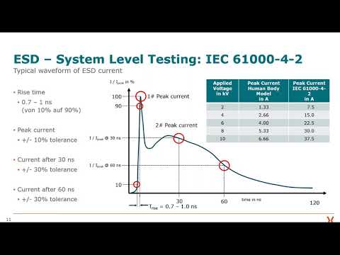
What is the IEC 61000 4 2?

FULL PCB MANUFACTURING Quote

The IEC 61000-4-2 standard defines ESD protection, by integrating two  testing methodologies. The contact discharge methodology discharges an ESD pulse from the ESD test gun that is in contact with the device under test. This methodology is highly preferred. The second methodology which the IEC 61000 4 2 makes room for is an air discharge. This methodology is ideal for scenarios in which it is impossible to maintain contact discharge testing.

The air discharge test involves bringing the ESD test gun close to the device under test until there is a discharge. These standards must be defined in such a way that each level is equivalent. Therefore, a Level 4 contact discharge of 8 kV is the same as an air discharge of 15 kV.

The IEC 61000 4 2 is an ESD immunity compliance standard for electronics that need to get the UL, CE Mark, and other certification. Electrostatic discharge ESD occurs everywhere. It occurs between high density electronic components in electronics products like television and mobile phones. It is impossible to predict ESD. Therefore, it is important to take some measures that prevent malfunction or damage of a device when ESD occurs.

The IEC 6100 4 2 is the most popular standard for evaluating robustness and approving commercial electronics. This standard is an effective EMC test standard needed to attain a CE marking. With IEC 6100 4 2, electronic producers can sell their products in Europe.

YouTube video

What is the Importance of ESD Protection in Electronic Products?

Like it was earlier explained, ESD can cause significant damage to electronic equipment and as such, this could lead to a catastrophic failure in the field. In the electronics manufacturing industry, minor mistakes or errors can be detrimental to the functionality of electronic components and devices. ESD damage is one of the most common causes of product losses.

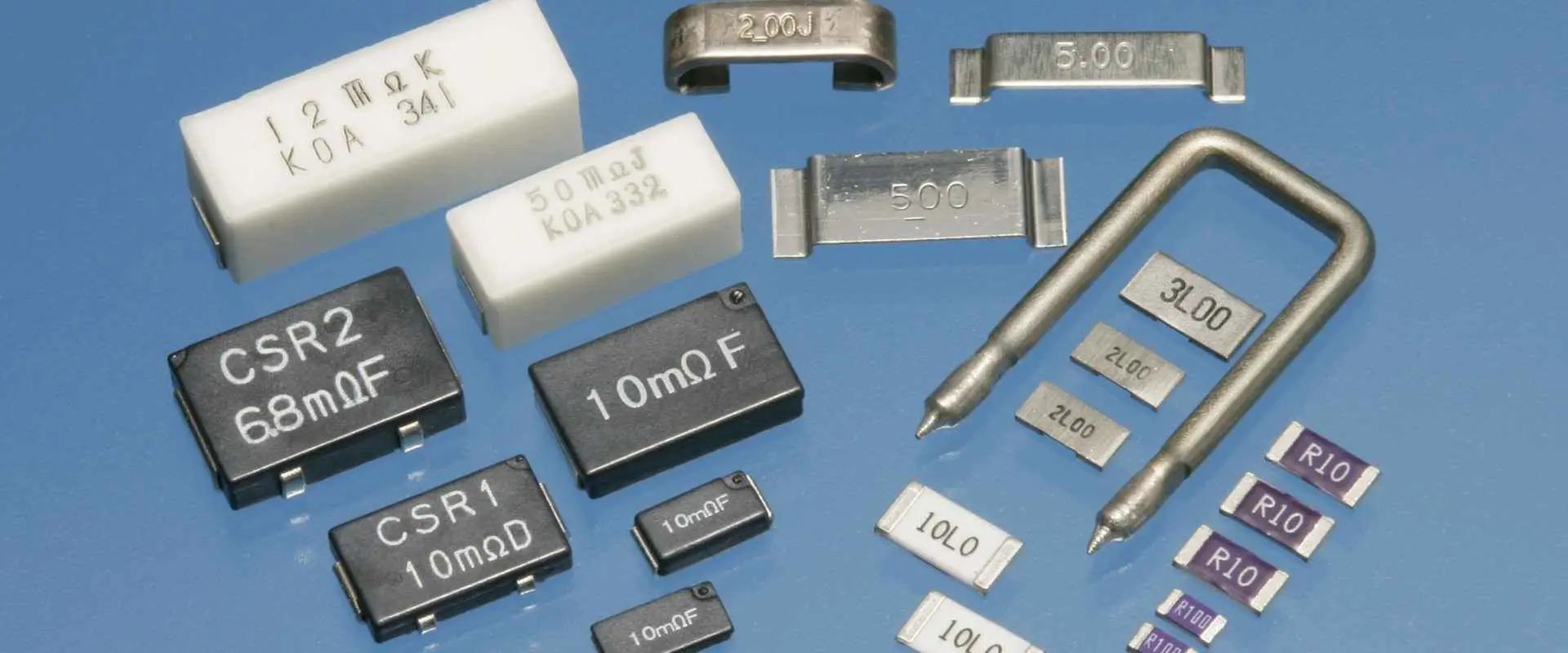
Electrostatic discharge (ESD) occurs when built-up charge releases between objects, thereby, resulting in the flow of electricity between these objects. ESD of charged objects caused by humans statically charged objects can cause damage to different semiconductor parts which include CMOS IC chips, MOSFETs, and diodes.

In most cases, 60 to 90 percent of damages caused by ESD doesnโ€™t cause complete failure. However, this damage can be difficult to detect. Therefore, it is of utmost importance to minimize and regulate ESD during circuit board assembly.

ESD protection is crucial in any electronic products as it helps to prevent any damage. Any electronic component or product is vulnerable to damage due to exposure to ESD. Also, ESD protection is crucial in preventing the formation of static charge in electronic products. The main purpose of creating the ESD standards is to minimize the risk of damage to devices that are sensitive to ESD.

Furthermore, this protection is ideal for minimizing failure in electronic device and as well as enhancing the performance and reliability of delicate electronic components or products. Adhering to the ESD standards is crucial for industries that produce delicate electronic equipment. Therefore, the ESD standard is great measure to prevent and also address all ESD related problems.

Electronic companies need to adhere to all the procedures of ESD standards. Also, these standards should be integrated in the appropriate way.

How to Control ESD

There are some preventive and precautionary measures that can minimize ESD for electronic assembly. These measures include:

  • Make use of anti-static equipment and tools to prevent electrical charge conduction. Also, do not work on electronic device when there is electrical storm as this can increase the risk of ESD.
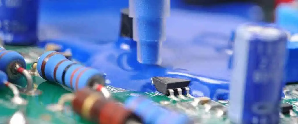
  • Circuit board rework or component repair should be carried out in an ESD safe environment.
  • Use ESD-safe tables or workstation to enable the dispersion of static electricity. Electrically conductive carbon fibers are used in manufacturing these mats. Therefore, ESD becomes inactive on the mat.
  • Wear a grounded wrist strap to minimize any risk of ESD incident. Ensure you wear this wrist strap correctly as it will protect any charge generated by the body.
  • ESD air ionizers can be used by engineers as they get rid of static charge from the air.
  • Employees may need to put on anti-static clothing to shield sensitive components and ESD shock.
  • Avoid using jewelry and some static accessories in the workstation.

Conclusion

The ESD standard for electronic assembly has helped in preventing some damages to electronic products. There are a wide range of standards set up to ensure safety and protection while using electronic products. Some of these standards are the IES 6100 4 2, ansi ESD s20 20 and the ISO 10605. Electronic manufacturers and assemblers should endeavor to adhere to these standards to ensure safety and reliability of electronic products.

What are the Features, Advantages, and Limitations of the Raspberry Pi Zero 2W

You can find different Raspberry models present in the marketplace. Raspberry continues to bring to us new models. Every one of these models has different features that ensure their uniqueness in different applications. The model released recently is the Raspberry Pi Zero 2 W.

Understanding the way this model functions is very necessary before going ahead to buy it. Furthermore, you must ensure that it works with your intended applications. Please read more so as to help you gain additional knowledge regarding the Raspberry Pi Zero 2 W.

YouTube video

Description of the Raspberry Pi Zero 2 W Model

The Raspberry Pi Zero 2 W can be described as the latest model of raspberry pi zero. It is a small and very powerful functional board. Also, it is a single-board and wireless computer that replaces the Raspberry Pi Zero W board. This board has a dimension of 65 nm by 30 mm by 5 mm. This is why it is known to be the smallest and high-performance raspberry pi board.

Back in 2015, the launching of the original Raspberry Pi Zero took place, and in 2017, the Raspberry Pi Zero W came to be. Few months after, the launching of the powerful Raspberry Pi Zero WH took place featuring the GPIO pins. While in 2021, the Raspberry Pi Zero 2 W was released. This particular model comes with similar features as Raspberry Pi3.

Features of the Raspberry Pi Zero 2 W include one mini HDMI port, one micro USB data port, and one micro USB power input. It can be viewed as a custom built system-in-package. In addition, this model is useful in different IoT projects, as well as smart home applications. Due to the small form factor present and its great power, the Zero 2 W model serves as a reliable computer for all your projects.

Furthermore, the Raspberry Pi features different high quality, as well as low cost adapters and cables. This allows users to enjoy their work. Also, Raspberry Pi Zero 2 W includes a Micro USB, which serves as its power source. This board comes with a great benefit of being compatible with the different Raspberry pi models. Even with its small size, it boasts powerful and great features.

With this board, it becomes easy for users to build different Raspberry Pi Projects.

What are the Hardware Components of Raspberry Pi Zero 2W

Raspberry Pi 3B
Raspberry Pi 3B

There is a need to familiarize yourself with the different components of the Raspberry Pi Zero 2W model.

RP3A0 SiP

This RP3A0 SiP is upgraded. It features a 64-bit quad-core Arm Cortex-A53 Central Processing Unit. Known as a very significant component of the hardware, the SiP is made up of Broadcom BCM2710A1 die with a 512 MB LPDDR2 SDRAM. This component is what makes the Raspberry Pi Zero 2W have additional single-threaded performance in contrast to the initial single-core Raspberry Pi.

GPIO

Raspberry Pi Zero 2W features 2 by 20 GPIO Pin sets. These pins offer excellent functionality such as digital Input and Output, SPI, PWM, and more. You might be required to solder the headers onto the GPIO headers if there is a need to make use of it.

Mini HDMI

The other models have an HDMI connector. However, this model is different. This is because it features a mini connector, which conserves space. The mini converter is very important when connecting your Raspberry Pi Zero 2W to your television.

MicroSD Card Slot

This is another excellent interface of Raspberry Pi Zero 2W. It provides support to data storage having a maximum of 32GB cards.

Wireless module IC

The Raspberry Pi Zero 2 W has on-board connectivity of both Bluetooth and WiFi. Its bluetooth is the 4.2 version, and it supports BLE.

Micro USB port

There is a micro USB port present on the left hand side which aids data communications and transmission of data. Using the USB OTG cables, connect these devices.

Camera serial interface connectors

This indicates the interface found between the processor of the RPI and the camera. You may utilize the 15-pin ribbon cables for connecting the module of the Pi camera onto the camera connector.

Best Project Ideas for Raspberry Pi Zero 2W

Here are great project ideas for Raspberry Pi Zero 2W.

Build a game station

Although the Raspberry Pi Zero 2W is a small size computer you can carry about, you can use it to build a game station you can carry in your pocket. The Nintendo 64 which is popularly used for building game stations features 4M of RAM. Raspberry Pi Zero 2W features 512M of RAM, a perfect feature for retro-gaming.

You can use the Raspberry Pi Zero 2W as a game console by simply plugging it on a TV. There are limited ports on this Raspberry Pi model. With a USB adapter and an HDMI adapter, you can easily include one game controller. However, you won’t have any port left. Developing a game station isnโ€™t a difficult thing to do. Applications like Recalbox and Retropie can be complicated to install.

Design cheap security cameras

This is one of the projects you can get done with the Raspberry Pi Zero 2W. Most security cameras are usually pricey. Also, users need to subscribe to make use of these cameras appropriately. However, most people donโ€™t know they can easily build their own cameras without having to spend too much. If you have got a basic camera module and the Raspberry Pi Zero 2W, you can build your security camera.

Since the Raspberry Pi Zero 2W is small in size, you can easily hide it discreetly. This choice is perfect for building the security camera.

Building of robots or drones

When you are building drones as well as robots, weight and size could become a major problem. Furthermore, another important thing to consider is power drain. For applications like this, the Raspberry Pi Zero 2W serves as a reliable option.

This microcomputer has a small size, is lightweight, and usually consumes lesser power. This option is much better when compared to Raspberry Pi 3B. In addition, Raspberry Pi Zero 2W allows space saving. It has a weight of 11g as well as offer high performance. Moreover, if a header is attached, it will have additional weight.

Hosts the file server

For home servers, you may utilize Raspberry Pi Zero 2W. Also, you will be able to host file servers using different options. One of these options is starting with the small distribution as well as install the Samba services. Moreover if you donโ€™t know much about text editors and command lines, there are easier alternatives.

You can try using NextCloud if your files arenโ€™t many. NextCloud is a backup solution since it instantly sends any file created on your computer to the server.

Block ads on your network

One of the project ideas recommended for Raspberry Pi beginners is the installation of an ad-blocker. You can use a Raspberry Pi Zero 2W to block ads on your network.

Ideal for music player or media center

This is another great project idea for your Raspberry Pi Zero 2W. If you have no smart TV in your home, simply install an app on your Pi model to make a good media center. The Raspberry Pi Zero 2W is a powerful and discreet minicomputer you can easily attach behind your TV.

Build binary clock

With the Raspberry Pi Zero 2W, you can build a binary clock. A binary clock uses binary to tell time. Children can easily familiarize themselves with numbers as they learn to tell the time. With the use of binary clocks, your numerical skills can be sharpened. In order to carry out your project effectively, you will require a Raspberry Pi Zero 2W and a Unicorn pHAT.

Understanding Broadcom BCM2710A1 SoC (BCM2710)

FULL PCB MANUFACTURING Quote

This forms an important component of Raspberry Pi Zero 2 W.

As an SoC, it makes use of different computer parts and components that work individually in the larger computers. Take for example, desktop computers may feature southbridge chips, separate processors, as well as graphics cards. All these are combined inside a chip.

The BCM2710A1 is made up of so many parts. Below are its major parts.

  • USB 2.0 PHY
  • GPIO Interface supports SPI, I2C, UART, GPIO, PWM)
  • 1 Giga Hertz quad-core, 64-bit ARM Cortex-A53 Central Processing Unit
  • VideoCore IV GPU
  • MIPI CSI-2 Camera Serial Interface
  • MIPI Display Serial Interface is not exposed on the Pi Zero W2!

Furthermore, it utilizes the 40nm silicon technology node. This node consumes more power than a 28nm node. Also, it offers less performance when it is in a similar power envelope.

Advantages of Raspberry Pi Zero 2 W

The Raspberry Pi Zero 2 W has more benefits when compared to some Raspberry Pi Zero.

Space saving

Raspberry Pi Zero 2 W is a very small board with less weight. This minicomputer is ideal for applications where space and weight is an issue. Because of its small size, it could be utilized discreetly in some projects.

Great power efficiency

Although the computing power of Raspberry Pi Zero 2 W is similar to that of a standard Pi 3B, Raspberry Pi Zero 2 W consumes less power. When this board was tested, it was very efficient. It has a fairer performance per watt than other Pi platform. Its idle current is lower than Raspberry Pi 3B and a bit higher than the Zero W. The board serves as a reliable option whenever you need to make use of less power as well as optimize the life of your batteries.

Cost

This is a board with low cost that provides great performance. Because it is not pricey, it is budget friendly. Even with the price, it still delivers great functionality and performance compared to the remaining models

Other benefits include the following

Wireless LAN and bluetooth connectivity are possible with the connectivity ports. This is why they work for different IoT projects as well as smart home applications

It has a small board and it user-friendly.

What are the Cons of the Raspberry Pi zero 2 W

Raspberry Pi zero 2W provides great benefits to users. However, it also comes with some cons, which will be highlighted below. Let us consider them.

  • Absence of Ethernet
  • One HDMI output, which wonโ€™t work for some applications
  • Display port is absent
  • You need to solder its header onto the Raspberry Pi Zero 2 W
  • Limited RAM
  • The camera does not have an adapter cable
  • Analog audio output is absent
  • 4K HDMI output is not included
  • The micro USB port and USB devices are too close

Related Questions

What is the best operating system for the Raspberry Pi Zero 2W?

Different operating systems can work for the Raspberry Pi. Moreover, the Raspberry Pi Zero 2W stands out and needs lightweight options such as DietPi and the Raspberry Pi OS Lite. Also, these are ideal options for any device with low specification. Apart from the above options, other operating systems that are lightweight are available for the Raspberry Pi Zero 2 W.

What are the ways of programming the Raspberry Pi Zero 2W?

This is a reliable and useful board which explains how you can program. The board provides support to the different languages for programming. To utilize this board, you will need an integrated development environment.

What areas are the Raspberry Pi Zero 2W Applicable?

Raspberry Pi Zero 2W can be incorporated as the desktop computer. This is great for use in all embedded applications. In addition, you can use it in building the robots, IoT wall devices, and more.

Conclusion

Although the Raspberry Pi Zero 2W comes with an extremely small size it provides strong and powerful features. The board ensures the easy building of different Raspberry Pi projects. Also, it is a low-cost single board computer that has a small size and works with different embedded applications and IoT projects.

What are the Color Bands and Applications of a 4.7 K Resistor?

SMD Resistor

You must be wondering what the colorful stripes found on the resistor really means. Or you really wish to know what functions the 4.7K resistors serve in electronics. Here we are to explain the ins and the outs of the 4k7 resistors. These include their applications and basic properties.

What Does a 4.7 K Resistor?

The 4.7 k resistor can be described as any electronic component that has a resistance of 4700 ohms or 4.7 kilo-ohms. This โ€œkโ€ is seen in 4k7 means kilo which indicates 1000. A resistorโ€™s resistance can be measured in ohms which is an electrical resistance unit. Resistors are useful in limiting the electric current flow in circuits and are usually utilized in different electronic devices.

You can easily recognize the 4.7k resistor due to its unique pattern of violet, yellow, red, and violet color bands. Furthermore, the band versions 5 and 6 comes with a pattern of violet, yellow, brown, black, followed by its temperature coefficient band and tolerance band on the band version 6.

There is one difficulty with the resistance 4.7 k ohm resistor. This is happening because you can easily confuse it with the 470 ohm resistor. Therefore take note of this and verify mak8ng use of the multimeter or color codes where necessary.

Color Bands of the 4.7 k Ohm Resistor

Resistor Wattage

Every band found on 4.7 kilo ohm resistors comes with a unique purpose. Regardless of the number of bands present in them, all the color-coded resistors have a minimum of two digit bands. One is a multiplier band, while the other is tolerance. This structure forms the four-band resistor color codes; the five as well as six band resistors usually add to the basic structure.

In four band resistors, the initial three digits will give the nominal value of the resistor. While the fourth band will give the resistorโ€™s tolerance. Although the resistor comes with the nominal value of 4.7k ohm, its actual resistance would vary a little bit below or above its nominal value. This tolerance reveals to us the expected range. Resistors of higher quality features improved tolerance over the ones with lower quality.

In the five band resistors, the initial four bands will reveal the resistorโ€™s nominal value. Take note that the extra band of the resistor helps in adding a specific digit to its nominal value. Consider this as an additional digit which has been added into the front, with other bands that retains similar functions as the four band resistor. Also, the final band, which is the 5thย band, identifies tolerance.

The six band resistor helps in adding a new color band at the resistorโ€™s end, which reveals the coefficient of the temperature. This indicates the resistorโ€™s sensitivity to changes in temperature. All resistors come with its own tolerance value. This means the value may not be 4.7 ohms exactly. Resistors with higher quality feature tighter tolerances.

4 Band Vs. 5 Band 4.7 k Ohm Resistor

According to our explanation, four band resistors feature two bands for the value. The first value is the tolerance while the second value is for the multiplier. Five band resistors feature three different bands for the value in which one is for the tolerance and one is for the multiplier.

The process of analyzing the five band resistor is similar to the four band resistor. Therefore, you have to look for any gap between the fourth band and the fifth bands. However, the last band in the four band resistors reveals the tolerance. You can then use the first four bands to get the resistance value.

There should be an order of violet (7), brown (x10), yellow (4), gold or silver (+-5% or 10%).

What is Resistance Tolerance of 4.7K Resistor?

The tolerance of a resistor indicates the resistance value of a resistor can feature. Therefore, the tolerance of a resistance 4.7 K ohm resistor depends on the specific series and the manufacturer of the resistor. 4.7 K ohm resistors have common tolerances which are 10%, 5%, and 1%.

  • For a 4.7K resistor with a 10% tolerance, the actual resistance ranges from 4.23k ohms to 5.17k ohms
  • For a 4.7K resistor with a 5% tolerance, the actual resistance ranges from 4.46k ohms to 4.935K ohms
  • For a 4.7K resistor with 1% tolerance, the actual resistance ranges from 4.653 ohms to 4.747K ohms

Common Applications of 4.7K Ohm Resistors

FULL PCB MANUFACTURING Quote

The 4.7K Ohm resistor is widely used in different applications. This resistor serves a lot of purpose.

Voltage dividers

4.7K ohm resistors is widely integrated in voltage dividers. These resistors produce a particular level of voltage. Also, there are two resistors on series in a voltage divider and the output voltage is very proportional to the two resistor values. Due to the tolerance level and availability of 4.7 Kilo ohm resistors, they are ideal for use in voltage dividers.

Current limiting

Also, you can use 4.7K ohm resistors to limit current. For instance, these resistors can help to restrict the flow of current via an LED. They can as well prevent the occurrence of overvoltage in a microcontroller input.

Pull-up or pull-down resistors

These resistors also serve as pull-down or pull-up resistors in digital circuits in order to ensure the maintenance of the voltage level of a signal. This is possible even in cases where you canโ€™t actively drive the signal. Therefore, 4.7K ohm resistors can prevent floating in input signals which is caused by an unexpected behavior.

Oscillator circuits

Another use case of a 4.7K ohm resistor is in oscillator circuits. This resistor helps to set the frequency of an oscillator. Also, you can use this resistor with other components like transistors and capacitors to produce a particular frequency signal.

Analogue Signal conditioning

4.7k ohm resistors serve some purposes in analogue circuits. These resistors are suitable for signal conditioning circuits as they help to adjust offset or gain of an input signal.

Conclusion

You can easily learn the color code of the 4.7 kilo ohm resistors for all resistor types. This distinctive pattern of violet and yellow band makes you spot them easily. Moreover, you may confuse them with the 470 ohm resistor that features violet and yellow bands. Therefore, it is very necessary that you verify making use of a multimeter or color code if possible.

Everything You Need to Know About CTBGA (Thin Chip Array Ball Grid Array)

BGA Chip

These days, almost all electronic devices, gadgets, and equipment are exclusively using compact, mini-size PCBs along with small variations. These PCBs incorporate various mini-size SMT components all around the surface of a PCB. Moreover, the BGA technology utilizes an under-side package of IC or pin-outs for connection rather than using the corners of an IC package.

Thus produced an HDI Printed Circuit Board, small size and lightweight dimensions product. The HD interconnects arrange in an array pattern directly under the package, which forms the pin grid. This enables the IC of a BGA to take less area over the surface of a PCB, enhances the performance, and gives more functional features in a PCB.

CTBGA stands for Thin Chip Array BGA. It refers to a type of IC package which is used in many consumer electronic devices. These devices include smartphones, tablets, and portable and wearable miniature devices. This article gives you a detailed insight into the advantages and features of CTBGA, along with its usage and applications.

CTBGA serves as an IC package that helps in making portable consumer devices lightweight and compact. It works similarly to a typical BGA package but has the size of the package and thinner chips. The package of CTBGA generally consists of copper traces, ceramic material, and a solder balls layer over the bottom of a package.

YouTube video

Benefits Of CTBGA (Thin Chip Array Ball Grid Array)ย 

BGA offers various significant benefits which enable it as a popular choice in the electronic industry. Some of those advantages include:

ยท High Density

Today, various consumer electronic devices require tiny packages with various pins. Because of this feature, engineers invented surface-mount Dual-in-line packages and Pin Grid Arrays that give track lower density. However, manufacturers of PCBs face many challenges. Pin bridging is among them. BGA, however, allows us to overcome this problem as the BGA solder balls provide the appropriate soldering needed for placing the package. Therefore, they place solder balls close to each other. This provides strength to the interconnects and minimizes the PCB footprint. BGA components create high-density interconnections which use the surface of a PCB effectively.

ยท Reliable Construction

The pins of the PGA package have a fragile and thin structure. Thus, resulting in the bending and damaging of these pins. Whereas, this is not the case with the package of BGA. In the BGA package, the solder balls are incorporated over the solder pads, which enables the network to be more reliable.

ยท Excellent Performance At High Speeds

In the BGA package, all the soldering balls are placed close to one another, which creates a close connection between components, minimizes signal distortion, and strengthens the interconnections during high-speed tasks. This shows that the network provides greater electrical conduction over high speed.

ยท Less Component Damage

Unlike PGA, the heating process melts BGA solder balls which enables them to connect with the Print circuit board. This, however, aids in minimizing the risk of component breakdown or damage.

ยท Reduce Overheating

The packages of BGA contain various thermal networks that dissipate the heat from the ICs. Thus, this effectively minimizes the risk of overheating.

Cons Of CTBGA (Thin Chip Array Ball Grid Array) 

chips-bga

BGA also comes with drawbacks, like all other electronic devices. However, the drawbacks include:

ยท Difficult To Inspect

BGA is basically a tiny material piece that allows the manufacturer to place the die of an IC over it. Because of the tiny size of BGAs, the inspection of soldering joints becomes difficult through visual inspection. However, X-ray machines and advanced microscopes may help in solving this problem.

ยท Prone To Stress

Circuit boards give flexural stress, which further affects BGA. Though, this stress causes reliability issues.

ยท Excessively Expensive

The soldering process of BGA packages requires highly expensive equipment. This, however, makes the BGA packages more expensive. Furthermore, manual soldering is used in packaging but in extremely lesser numbers.

All the above-mentioned advantages and features add up in the usage and application of BGAs. Thus, increasing the demand for Ball Grid Array packages. Though BGA devices use advanced types of technologies, they are skeptical of failures. Therefore, inspection of every joint on the board minimizes the process of rework. If you are thinking of incorporating BGA into your device. Then choose trustworthy, reliable, and industry-leading manufacturers. Various companies offer a vast range of customizable BGA packages.

Applications of CTBGA (Thin Chip Array Ball Grid Array) 

Various consumer electronic devices use CTBGA technology. These consumer devices include smartphones, wearable devices, and tablets. Some common usage and applications of CTBGA technology include:

ยท Mobile Devices

Because of the higher pin count and small size of CTBGA, manufacturers tend to use them in devices like tablets and smartphones. Moreover, applications like memory, processing, and connectivity also employ this technology.

ยท Wearable Devices

Wearable devices like fitness trackers and smartwatches use a wide range of CT BGA packages because of their low consumption of power and compact size.

ยท Consumer Electronics

Consumer Electronics like digital cameras, gaming consoles, and MP3 use CTBGA packages in them. This happens because of their cost-effectiveness and higher pin count.

ยท Automotive Electronics

Automotive electronics like infotainment systems and engine control systems also employ CTBGA advanced packages. This, however, happens because of their high thermal conduction and high-reliability features.

ยท Medical Devices

Because of the higher pin count and small size, many manufacturers use CTBGA in medical devices. However, these devices include diagnostic equipment and portable medical devices.

Conclusion

CTBGA stands for Thin Chip Array BGA acts as an advanced IC packaging. It is widely used in consumer electronic devices, which include tablets, smartphones, and mini-portable devices. Additionally, it offers various benefits and features. 

These features include high thermal conduction, higher pin count, high reliability, small size, and low cost of manufacturing. Generally, The advanced CTBGA packaging is commonly utilized in wearable devices, medical devices, automotive electronics, and consumer electronics. CTBGA plays a vital role in enhancing the demand for lightweight, high-performance, and compact devices.

Why is the Zenit PCB Tool Great for Professionals and DIYers?

Cheap PCB Manufacturer

Zenit PCB could be a very great tool for DIYers and professional designers of electronic circuits who wish to conduct a test on their designs before animating it physically. It is a PCB design tool that is Windows compatible and allows designs up to a thousand pins.

What is ZenitPCB Suite Composed of?

Zenit PCB Suite was designed for those that wish to make PCBs as a hobby or for academics and students from high schools or universities who wish to create their personal printed circuit boards with an expert approach. Particularly, this is achieved without paying for any expenses like licenses.

In addition, the full ZenitPCB suite is made up of many tools. Its layout tool allows you to design the major layout of your printed circuit boards by utilizing different components. The Zenit Capture Schematic tool is also available. This allows the user to select the circuitโ€™s components and then create a unique netlist. Also, you can find the ZenitPCB tools in a specific library called the ZenitPCB parts. This software also has the ability to read the Gerber files using its tool called the PCB GerberView.

What Does Zenit PCB Layout Mean?

Zenit PCB Layout can be described as a great tool for creating a professional PCB. This tool is a CAD program that is easy and flexible to use. It allows users to achieve their dream projects within a short period. In addition, it is fully freeware for semi-professional or personal use, which are limited to about 800 pins. It forms a borderline between professional and hobby jobs.

Using the ZenitPCB Layout, you can create your project right from the layout or its schematic capture. This is a great software for PCB layout designs for creating top-notch printed circuit boards. ย The first step here is to import the netlist (this is a ASCII file that contains the electrical information) from several schematic captures (Eagle, Protel, Pads, Orcadโ€ฆ), with the components as well as their electrical connections.

For the second case, you will be able to realize the project from your layout editor directly, import the components out from its library as well as directly connect all the pins with its cursor. Therefore, it is possible for users to create boards without having to import the netlist from the Schematic Capture. The ZenitPCB Layout has the requirements for achieving a reliable printed circuit board, makes use of the general or individual project, via the net class. You can find some of the features of a PCB here.

Now, to have better control of your project, you will be able to review the created Gerber via the Zenit PCB Gerber View.

What are the Benefits of the Zenit PCB Layout?

Zenit PCBโ€™s user interface is compact, despite its numerous application quick keys and buttons. Also, it has the major workspace at the center. On its top area, and underneath the menu bar, you will find many quick-access keys which allows users to add new circuit parts, print, save files, search, etc. Its left panel is made up of some project-related information which includes parts library, available projects, as well as available netlists.

On your workspaceโ€™s right hand side you will find shortcuts for several operations, such as drawing a circle, square, or a line in your schematic, addition of text, etc. This workspace also allows the simple drag-and-drop function; therefore it is easy to handle the tool. Zenit PCB layout is a great tool and a complete freeware for semi-professional or personal use.

What is New in Zenit PCB?

Zenit PCBโ€™s latest version comes with many improvements having all its issues fixed within all tools. Furthermore, there are new functionalities introduced. Among the significant upgrades includes the inclusion of 200 extra pins. This allows the users to utilize 1000 pins rather than the 800 pins present in the initial version.

For the ZenitCapture Schematic Tool, there are features such as auto change of the parts values, auto renaming of the net wires, the locking of all open projects, placed parts listing, alternate text printing, as well as black printing.

Furthermore, this software allows 1300 symbols. Some of the newly added features to the Gerber View of Zenit PCB include the hiding of the layers during the view, the mirror view, print preview, printing holes and printing in black.

How to Use Zenit PCB

FULL PCB MANUFACTURING Quote

To begin your new project, click on file, which is found on the menu bar and then click on New. This opens a workspace on ZenitCaptureโ€™s Schematic tool. This workspace can be described as a sheet having black and green borders that gives the location where the elements will be placed. You can then choose the components and create the circuit schematic.

First of all, click that desired element and also click the workspace so as to position it. Once the first component is added, youโ€™ll notice a positive (+) sign appear beside the Parts option which is situated on the left panel. This option can be expanded to check all the added elements. You can connect the elements by connecting a componentโ€™s connection point to the other by dragging your mouse. Once you are done preparing the schematic, you will have to pack iy inside a netlist.

Next, open your new project using the Zenit PCB Layout tool and then select the dimensions and size of the PCB you desire. You can achieve this by clicking on Place which is found on the toolโ€™s top menu and then select Board Wizard. Then, set up the components on your layout board. Next, click on File and under Import, select Netlist.

To view the Gerber files, click on the GerberView button of the ZenitPCB and select the file. This program will be able to open the NCDrill and Gerber files as well as offer visualization with respect to the ASCII format.

Conclusion

Zenit PCB is a reliable tool for all practical circuit designs. You can explore all the available options to help you discover the possibilities that the software can offer you. Zenit PCB Suite was designed for those that wish to make PCBs as a hobby or for academics and students from high schools or universities who wish to create their personal printed circuit boards with an expert approach.

Exceptional Advantage of Using XC6SLX45-2FGG484C In Your Project

Xilinx FPGA Chip

FPGAs are gaining popularity due to tier-unique features. You can find several FPGAs in the market with different specifications and features. Today we are talking about XC6SLX45-2FGG484C. The manufacturer of XC6SLX45-2FGG484C is Xilinx, a leading company in Field-Programmable Gate Arrays (FPGAs) and related technologies. Xilinx is a well-known FPGA manufacturer, and the XC6SLX45-2FGG484C is one of the many FPGA models they produce. Moreover, It belongs to the Spartan-6 family. Let’s dig deeper to learn more about

Specifications of XC6SLX45-2FGG484C

This FPGA has 43,661 logic cells. These are the basic building blocks of the FPGA.

  • This amazing FPGA also has 6,912 slices along with 180 DSP Slices.
  • Mb block and RAM supports data storage. That’s why data storage is no more issue.
  • Four Clock Management Tiles are part of FPGA
  • It operates 400 MHz frequency

Alphanumeric Breakdown Of FPGA

Xilinx Evaluation Board

 Following the breakdown, the alphanumeric code XC6SLX45-2FGG484C is for you. Because many people consider these alphabets and numeric just numbers and alphabets, actually, they have significant means.

Here’s what each part of that part number represents:

  • XC Represents the product family, which in this case is the โ€“ Spartan6 FPGA by Xilinx. This company is well known for making programmable logic devices.
  • 6 represents the generation of the Spartan family. In this case, it’s the sixth generation.
  • LX45 indicates the device’s size and speed grade. In this case, it has 4,608 logic cells and belongs to the -2 speed grade. As a result, you may experience amazing speed.
  • 2 Indicates that -2 speed grade. It is moderate speed.
  • FGG484 Indicates the package type, which is a Fine-Pitch Ball Grid Array (FBGA) with 484 pins. Most of the FPGAs come in ball grid arrays. It is compact and easy to integrate systems.
  • C shows the temperature range of the device, which ranges between 0ยฐC to 85ยฐC. As a result, it can work even at high temperatures.
  • So, altogether, XC6SLX45-2FGG484C identifies a specific model of the Virtex-6 FPGA from Xilinx. Its code represents 45,000 logic cells, a commercial speed grade, and a Fine-pitch Ball Grid Array package.

 Advantages Of Using XC6SLX45-2FGG484C

1. Unmatchable versatility

One of the biggest advantages of the XC6SLX45-2FGG484C is its versatility. As an FPGA, it can be programmed to perform a wide range of different tasks. Unlike an Application-Specific Integrated Circuit, which is designed to perform a single function and cannot be changed once it’s been manufactured, an FPGA can be reprogrammed as needed. This makes it a great choice for applications where the requirements may change over time or where different tasks need to be performed on the same hardware.

2. Exceptional performance

ย How can an FPGA provide the best and most exceptional performance? It’s all because of its exceptional feature. That’s why it is advantageous to use XC6SLX45-2FGG484C. It gives you performance. It functions at a maximum clock frequency of 550 MHz; it can handle complex tasks quickly and efficiently. It also has a relatively large number of logic cells, i.e., 44,200. This number of logic cells is good enough to perform logic functions. A similarly large amount of Block RAM of 2,592 Kb makes it suitable for demanding applications.ย 

 Video processing or high-speed networking is an example of its high speed. Above all, it has a superior architecture.

3. User-Friendly Features

 Many people think that FPGAs are hard to handle. But this FPGA is easy to use. User-friendly features make it an ideal choice for FPGA. In addition, it also adds to its performance and versatility. The XC6SLX45-2FGG484C also has various features that make it easy to work with. For example, it has a built-in Power-On Reset circuit that ensures the FPGA uses normal power. It is initialized properly when power is applied. Moreover, it also has a JTAG programming interface. As a result, they can do easy programming and debugging.

4. Well-Organized Power Management System

Every FPGA comes with this unique feature. You can’t expect any FPGA without this feature. The XC6SLX45-2FGG484C FPGA also consumes low power. This FPGA features a dynamic power management system. That’s why it can adjust power usage based on the workload. Its dedicated power management interface is just the icing on the cake. It allows users to monitor power consumption in real-time. If the device is not working, then this system adjusts power. As a result, there is no power loss. The low power consumption of this FPGA makes it ideal for battery-powered applications. That’s why many IoT devicesย have this FPGA.

Some Frequently Asked Questions

FULL PCB MANUFACTURING Quote

ยท How Can a Hobbyist Use This XC6SLX45-2FGG484C?

The XC6SLX45-2FGG484C is a relatively mature product. As a result, there is a wealth of information available on how to use it effectively. This includes documentation, tutorials, and support from Xilinx and the broader FPGA community. This is a huge advantage for engineers who are new to working with FPGAs or who need to get up to speed quickly on a new project. That’s why you are a seasoned engineer or hobbyist. You can use it XC6SLX45-2FGG484C.

ยท What Is the Packaging Type of XC6SLX45-2FGG484C?

This FPGA comes in the FBGA-484 package. The ball grid’s airy and compact package makes it ideal for many devices. Most FPGAs come in FBGA packaging. It is based on innovative technology. BGA packaging is safe and compact. This packaging has a dimension of 23mm x 23mm. Above all, it is sturdy and standardized packing.

Concluding Remarks

XC6SLX45-2FGG484C FPGA has unique architecture. Its low power consumption and memory option make it ideal for various functions. As a result, it has better chances to incorporate in different systems.

Overall, the XC6SLX45-2FGG484C is a versatile, high-performance FPGA. As a result, it is easy to work with. Its combination of performance, flexibility, and ease of use make it a great choice for a wide range of applications. The scope of us is very high; for example, from video processing to high-speed networking to industrial control systems, it has the potential to adjust. Whether you’re a seasoned FPGA engineer or just starting out, the XC6SLX45-2FGG484C is definitely worth considering for your next project.

How Thick Should a PCB be?

Thick PCB

How thick should a Printed Circuit Board (PCB) and what is the baseline or standard for it? What are some of the reasons influencing the importance of a circuit boardโ€™s thickness?

A thick board can offer a wide range of benefits, such as supporting the resistance and conductivity capabilities of the PCB. Everything you need to know about the standard thickness, the benefits of the same and some of the special considerations are discussed in this article.

What is PCB Thickness?

It refers to the toughness or higher elasticity of the Printed Circuit Board (PCB). This has become a standard practice among many circuit designers, as it helps to increase the boardโ€™s resistance to damages.

What is Standard PCB Thickness?

It refers to the baseline or minimum thickness of PCB. Without this, it might be impossible to gauge whether the board can comfortably withstand some of the things and exposures it could have been exposed to.

The standard thickness is 1.577, which is the same as 0.062 inches. The reasons for the adoption include:

  • It is a historical standard size for circuit boards. It dates back to the days of Bakelite Sheets.
  • This standard thickness is also used across different facets, especially in the electronics industry, where it is used for both consumer electronics and related products.

The Variations to Standard PCB Thickness

pcb copper thickness

Despite the historical advantage and the widespread usage; the 1.57mm size is not the only one you can find out there. Today, different variants are in existence. Examples are:

  • 3.17mm or 125 mils
  • 2.36mm or 93 mils.
  • 0.031 inches or 0.78mm
  • 0.03 inches or 2.36mm

What is the PCB Thickness Tolerance?

The ideal tolerance is 10% for the base thickness of 1.57mm. The tolerance can also vary, depending on the applications, the types of circuit boards and a couple of other design and manufacture factors.

How to Determine the Thickness of PCB Layers

The layers of the circuit board also have a role to play towards the accurate measurement of the thickness. For context, the higher the number of layers used, the more difficult it becomes to get the right dimensions.

The layers of the PCB can range between 2 and 32. Out of this, the considerations for the thickness range from resistivity, conductivity and mechanical weight.

PCB Copper Thickness

The copper (material) used in the circuit board can also influence the thickness of the board. Mostly measured in ounces, the thickness of the copper ranges between 0.5 oz and 2 oz. it is also common to have the measurement ranging from 1 oz and 2 oz.

The Factors Influencing Thick PCB

FULL PCB MANUFACTURING Quote

A circuit board is not thickened without a purpose. Certain factors, parameters and considerations influence how thick the board becomes.

The following are some of the common factors, broken down based on the roles they play:

1. The Design Factors

How the PCB is designed can influence the outcome of the thickness. Here are examples of the design-centric factors:

2. Copperโ€™s Thickness

Also called the copper weight, it refers to the relationship between the current passing through the board and its thickness.

Measured in ounces per square feet, the base copper thickness is between 1 oz and 2 oz (1.4 to 2.8 mils).

However, the thickness of the copper can be modified depending on the following factors:

  • The addition of more copper, depending on the increased need to increase the currentโ€™s thickness.
  • The layer of the PCB increases as the weight/thickness of the copper increases.

3. Signal Types

What types of signals do the circuit board carry? Variations in the signal influence the boardโ€™s thickness in the following ways:

  • The type of required signals impact the types of materials the board uses.
  • Depending on the materials, the boardโ€™s weight can increase, especially if more (thick) materials are used.

The types of circuit boards are also considered here. For example, the High-Density Interconnect (HDI) boards using complex signals often have thinner footprints, thanks to the combination of the following:

  • Thin, high-performance materials.
  • Laser microvias and;
  • Thin traces.

On the other hand, the PCBs conveying high-power signals tend to be thicker, thanks to the following factors:

  • These boards use wider traces.
  • They also use thicker copper.

4. The Type of PCB Material

What type of material does the circuit board use? It plays an important role in the thickness. Worthy of mentioning is that the Flame Retardant 4 (FR-4) material is commonly used because of the flexibility and availability of the substrate in different thickness options. You can find the FR-4 materials ranging between 0.2mm and 3.2mm.

5. Size and Flexibility Concerns

The type of material used also has a hand in the outcome of the boardโ€™s weight. Worthy of mentioning is that the considerations are between the thinner and thicker boards, all based on the materials used.

The following are some of the discrepancies between the thick and thin circuit boards:

  • Rugged vs. Thin: thin circuit boards, such as the ones using the flexible materials are flexible, but pose a risk of lacking structural integrity. On the other hand, the thick PCBs are rugged.
  • Space Considerations: thin PCBs tend to take less real estate in the circuit board, because of the flexibility. The reversal is the case with the thick PCBs that take up a lot of spaces within the boardโ€™s real estate.

6. Viasโ€™ Type

The footprint created by the vias also plays a part in how thick the PCB becomes. Via in-pad, through via, buried via, blind via, and micro via are the common types of vias.

Despite the fact that these vias help to fast-track the routing of traces through the boards; they can also impact the size. For example, it is better to use the micro vias for the HDI circuit boards and the PCBs with thinner footprint.

7. How Many Layers Does the PCB Have?

The numbers of layers used in the circuit board also impact how thick it becomes. The general rule is that multiple layers equal more weight. Therefore, a multilayered PCB tends to weigh more and be thicker than one that uses a single layer.

  • A single-layer PCB weighs around 1.6mm, while the standard PCB thickness for 2 layers is higher.
  • Ideally, the 2-layer, 4-layer and 6-layer circuit boards often fall within the ambient of the standard PCB thickness.

8. The Operating Environment

Circuit boards adapt differently, based on the environments they are exposed to. Some contexts are given below:

  • Due to the less thermal stability, the thickest PCB is best used in low-current operating environments.
  • Both the flexible circuit boards and the ones with a thinner footprint are not ideal for use in rugged operating environments.

The Manufacturing Factors Influencing PCB Thickness

copper thickness

The processes that go into the production of circuit boards also impact how weightier the circuit becomes.

These are some of the manufacture/production-centric factors influencing the boardโ€™s weight:

Depanelization Method for the PCB

Depanelization refers to the process of separating jointed PCBs into individual circuit boards. Depending on the type of board, different depanelization methods should be used.

  • It is better to route the thinner PCBs, as a way of creating breakaway tabs.
  • The scoring depanelization method can be used to separate the thick circuit boards.

The Drill Hole Manufacturing Process

This has to do with the relationship between the drilling process and the underlying factors for making such holes in the PCB.

These are some of the considerations:

  • Aspect Ratio: this is the ratio or figure highlighting the difference between the drill hole diameter and the holeโ€™s depth.
  • The depth and diameter capabilities of the lasers and drilling machines also influence the hole-drilling manufacturing process.

Layer Stackup

How the layers stackup or are outline on the PCB? The PCB manufacturer should be able to create stackups of the layers, especially for the PCBs with thinner footprints.

End-Use Environment

Where will the thick PCB be exposed to or used at the end of the day? The rule of thumb is that the harsher the environment is, the higher the thickness of the circuit board should be.

A harsh PCB environment is underscored by the following:

If your PCBโ€™s use case is required for any of those environments, it means that you need to fortify it with more layers. This makes the board thicker, weigh more and have enough coverings to bolster the durability and reliability.

The PCB Assembly Process

The completion of the circuit board production process is not deemed over if the components have not been assembled.

At this point, the processes that go into the Printed Circuit Board Assembly (PCBA) have a role to play in the thickness.

Here are some noteworthy considerations:

  • The Wave Soldering process is best-suited for PCBs with thicker layers.
  • Consider using the Reflow Soldering process for the thinner circuit board layers. Doing so helps to aid heat or thermal energy transfer in the PCB.

Conclusion

The thickness of copper layer in a PCB can increase the boardโ€™s weight. Therefore, you should explain your layer requirements to the PCB Contract Manufacturer (CM). We will take your requirements into considerations, as a way of ensuring that the capabilities of the materials match the final PCB design.

What Does a Pick and Place File Mean?

Pick and Place File

This component placement list and Pick and Place File is very important for the right utilization of the pick and place machines. The pick and place data are necessary for the proper placement of the through-hole and surface mount parts on the circuit boards. This pick and place data can be described as the machine file that takes the text format of ASCII. This is composed of the X/Y locations, reference designator, rotation, the bottom or top side of the circuit board, etc.

The XY position or pick and place files are very useful for the automated placement of the SMT component. Also, you can program the pick and place machines manually, making use of a special camera guide. However, this could take a very long period, especially for boards having lots of components, which could lead to errors. With the Pick and Place file, you will be able to improve your accuracy as well as save time.

Pick and Place files can be basically described as the components present in their design as well as their x-y rotation and coordinates. Majority of the PCB design softwares can also help in extracting the orientation and location of the component from the layout file of the board. This produces your pick and place file.

KiCad Pick and Place File

.Schematic File

Whenever you want a machine to assemble YourPCB, you can create the position file for that machine to know where each part will be placed. The KiCad process could be a bit tricky; this is why we have decided to create a comprehensive article to assist you with the generation of a position file.

The first step is placing the โ€œPlace File Originโ€™. Search for โ€œPlaceโ€ and then select drill/place file Origin. Next, place this origin in the boardโ€™s lower left-hand corner side of the board. Note that, if it doesnโ€™t take a perfect spot in that corner, then it is nice so far it remains close.

Check the PCBNew section, select โ€˜Fileโ€™ and then select โ€˜Fabrication Outputs.โ€™ Then from there, choose Component Placement (denoted as .pos).

During the generation of these files, male sure that these settings are in place:

  • Format โ€“ASCIIUnits โ€“ Millimeters
  • Files โ€“ Separate the files for the back, front
  • Check โ€“ Make use of the place/drill file origin

There would be two different .pos files created. One of the files would be for the top part of the board while the other will be for the bottom part of the board. Now, these are the important files that we cannot but make use of.

What is the Pick and Place File Composed of?

Now, let us consider what the file is composed of.

  • Ref: This is the designator for your component. It is usually set in a schematic builder
  • Package: It is the footprint used when you are laying out your PCB
  • Val: This is the value of the component. It is usually set in a schematic builder
  • PosY: It is the Y-position with respect to its place origin
  • PosX: This is the X-position with respect to its place origin
  • Side: This is the side of that port where the part is on. Note that you must have two different files for the bottom and top.
  • Rot: It is the number of degrees that the part has to be rotated using the machine during assembly

If thereโ€™s a need to make changes to the .pos file, make sure you donโ€™t alter the file created. Only make changes in the layout and then create a new.pos file. The generated file is fed into the pick and place machine and it might not function effectively if you make changes to the format.

How to Generate Altium Pick and Place File

FULL PCB MANUFACTURING Quote

Accessing the Setup

You can access the dialog of your Pick and Place Setup in these ways outlined below. Click on File, then select Assembly Outputs, and then choose โ€œgenerate pick and place files from the PCB.โ€ Under โ€œAssembly Outputsโ€, which is seen in the Outputs section of the OutJob (denoted as *.OutJob), click the โ€œgenerate pick and place filesโ€ twice.

All Columns: This explains all the parameters where you can select from to be added to the output file. Then enable the parameterโ€™s Show column which you wish to add to the output. Also, the information of the location can be expressed in three different ways. This corresponds to those three methods though which the reference point of a component footprint may be specified inside your source PCB library.

  • Mid X, Mid Y โ€“ This coordinates for the center point of the component
  • Ref X, Ref Y โ€“ This coordinates for the user defined reference point of the component
  • Pad X, Pad Y โ€“ This coordinates for the Pad 1 of that component
  • The Grid Region: The grid region shows a preview of what information would be added to the output file.

Output Settings

Units: This region is used for specifying if you should use metric or imperial units when measuring the location coordinates of the component

  • Show Units: This shows the units
  • Formats: This shows the different formats (Text and/or CSV) from which you wish to generate the output.
  • The Separator: Choose your preferred unit separator out of the drop-down
  • Exclude the Filter Parameters: This enables the exclusion of the parameters utilized for the filtering
  • Include the Variation Component: This feature enables you to add variants.

When you click Ok, you will generate the pick and place files (.txt and .csv). These files would be stored in line with the defined output paths.

These files would be seen in the Projects Panel, which is located under the projectโ€™s Text/Generated Documents sub folder.

Tips

The dialog offers the capability to integrate custom filtering in order to remove some certain parts from the report. You need to select the filter icon to apply filtering. The filter icon is in a column header. You will realize that the subsequent menu comprises row entries to enable quick elective filtering. All you just need to do is to select the custom entry. This helps you to have access to the Custom Filter dialog.

Furthermore, you can integrate the dialog to indicate the rows of data to be displayed in the BOM according to the filtering criteria. The filter icon will change its color to blue once you have applied it. This means that the column in question is experiencing custom filtering. As required, add custom filtering to the other data columns.

What is the Significance of the Pick and Place File?

Pick and Place Files play a very significant role in the process of PCB assembly. Typically, it features the line number of the BOM, XYZ coordinates, reference designator, as well as each board componentโ€™s part number.

Also, the pick and place file is very important for the selective soldering and SMT placement machines. This happens before the process of assembly starts.

The circuit boards come manufactured in panels. Also, it is very important that you update your pick and place files continuously after each change has been made on your board.

Instructions Necessary for Pick and Place File Creation with Different Software Types

named pick place with .csv format.

Eagle Software

To create your pick and place file, run mountsmd.ulp. You may be able to view this file from the menu. Choose File then run the ULP from your dropdown list. This software would create this .mnt (mount top) as well as .mnb (mount reverse). The file also maintains the componentsโ€™ location coupled with the PCB originโ€™s coordinates. This file will be in txt format.

The Altium Software

The altium software is useful for creating an output for the pick and place that will be utilized during the process of assembly. To create the output, two options are available.

Create (*.outjob), which is the Output Job Configuration file. This creates an output generator that is well configured. Choose File from your menu. From your dropdown list, select Assembly Output, then โ€œGenerate Pick & Place Files.โ€

Once you click Ok, youโ€™ll see your output in the dialog box of your Pick and Place Setup. Note that the settings will be stored and kept safe in the config file. Moreover, when making use of the dialog of the Pick and Place Setup, these settings will be stored inside the project file.

Allegro/OrCAD Software

There is a similar procedure for the creation of pick and place files for either Allegra or OrCAD software. Select File from your menu. Then from the dropdown, click โ€œExportโ€ and then โ€œPlacement.โ€ Note that this procedure works with the most recent versions of Allegro or OrCAD software. The earlier versions might be different. Make sure you consult the documentation of the user to get more information.

Conclusion

In order to place the surface mounted components on the printed circuit boards through automated equipment, creating the pick and place file is very necessary. This helps in programming the equipment. The pick and place file has all the necessary positional parameters that this machine will know where this component will be placed as well as the orientation it would be on the printed circuit board.

A Guide to Comparison between PCB Potting Vs. Conformal Potting

pcb potting

Today, there is no electronic device existing that does not contain PCBs in its structure. The quality of the PCBs used in such devices directly relates to the normal functioning of the electronic devices later.

 It means all PCB manufacturers need to pay great attention while designing and producing PCBs. It is because the performance of minor to major electronic devices enhances with these PCBs. 

One way to make sure that the manufacturer is producing state-of-the-art PCBs is called PCB potting. In this post, we are going to have a detailed look at critical aspects of potting and how why it is important to ensure the quality of PCBs for integration into electronic gadgets.ย 

What is PCB potting?

pcb potting compound

You can define Potting for printed circuit boards as a quality-check method that minimizes any chances that can damage electronic devices due to faulty PCBs. There are different external factors like chemicals, heat, and mechanical wear that can lead to further damage if not treated in time.

 The process of potting includes a special potting material that functions similarly to a chemically formed encapsulation resin that secures the entire PCB board from the aforementioned complications. 

Now, letโ€™s discuss some prominent advantages of PCB potting below:

  1. Improves performance: One major benefit of using PCB potting is that it maintains the natural performance of electronic devices. It also boosts the circuit’s dependability by securing the printed circuit boards from possible threats, which include voltage issues, moisture, and alteration. Sometimes other factors like vibration and stress can create a negative impact on electronic devices, and potting helps with that as well. 
  2. Reduce vibrations: It means potting blocks the vibrations created due to printed circuit boards and their holders. In case these vibrations exceed the limit, they can exert stress on the printed circuit boards and lead them to ultimate dysfunction. 
  3. Tidy PCBs: The printed circuit boards can inculcate debris and dirt due to prolonged usage. Potting includes an encapsulated resin that helps in keeping the board tidy through all circumstances. Dirty and uncleaned PCBs can absorb more heat and hinder the signals, which hamper the performance of the electronic gadgets you want to use in. 
  4. Privacy: Electronic devices cannot function properly if they lack security. For this, PCB potting is the best possible solution. The process makes the PCBs accessible and combines with engineering to ensure impeccable protection of PCBs. 

Compound Guide for PCB Potting

Common Compounds

1. Epoxy

Epoxy is among the favorite potting materials used by many PCB manufacturers. It is because it offers different benefits. It is better to have a quick look at the following benefits offered by Epoxy resins for the potting process:

  • Epoxy has no parallel when it comes to adhesion
  • Such resins do not need primers that speed up potting for PCBs
  • They are excellent in tensile strength and stiffness
  • Epoxy resins are good for use in transformers and agricultural machines due to their impressive chemical properties. 

2. Silicone

Silicone is another trusted potting material common to use. There are different applications of silicone except potting for PCBs. You will see different PCB manufacturers relying on silicone for potting. The following pointers will help you understand why is that:

  • Silicone is good for potting because it has an impressive expansion ability
  • Silicone is soft, and you can easily amend it in any desired form
  • The temperature endurance of silicone stands the best when it comes to potting
  • Silicone is not an affordable potting compound, but it does not exert any stress on the PCB components at all

3. Polyurethane

We have Polyurethane which is among the commonly used potting materials. There are different reasons why Polyurethane is on this list. Letโ€™s find them out below:

  • Polyurethane is an expandable material that fits best for potting
  • It resists mechanical wear and possible damage to PCBs and their parts
  • It goes well with different natures of substrates due to its excellent flexibility

Merits and Demerits of PCB Potting Assemblyย 

FULL PCB MANUFACTURING Quote

The method of potting is not a hectic one to perform. It is among a few effective and fruitful PCB-relevant processes that drive out positive results. Especially those PCBs that need a durable quality check method; there is no better option than potting itself. 

The technique is also suitable for devices that need to avoid mechanical abrasion all the time. Potting enhances the longevity of these devices at the same time.

 Experts believe that you can also consider a potting method to make sure vibration dampening, regulated heat emission, and protection of PCBs and their components are in place.  

Choosing the Right PCB Potting Material

ยท Hardness

Since there are different potting materials available in the market, donโ€™t get stuck with choosing the best for yourself. One main factor in evaluating potting compounds is their hardness. 

  • If a potting material is tough, it will provide better protection against weather complications like heat and moisture
  • Hard potting materials are epoxy and urethane, along with silicone
  • Siliconeโ€™s hardness ranges from 10A-60A, and it’s the hardest material you will find on the market

ยท Thermal conductivity

Another factor is the thermal conductivity. You need to make sure that the potting compound you are going to select meets the following standards of thermal conductivity:

  • The compounds with an acceptable range of thermal conductivity are useful for potting.
  • Epoxy and urethane can prove to be beneficial in terms of delivering a good amount of thermal conductivity.
  • Silicone is the best with thermal conductivity and dissipates a large amount of heat produced by electronic devices, whether big or small. 

ยท Viscosity

A fine potting material must have the parameters of viscosity. In case you don’t know about them, check out the following pointers to learn about viscosity standards in detail:

  • The perfect encapsulation of PCBs works flawlessly if the viscosity is less.
  • If the potting material is self-leveling, it will contribute to achieving positive results.
  • The potting compound should be easily adjustable to avoid any problems, and this only happens if the viscosity of the compound is less.

ยท Color

You cannot ignore the color of the potting material. Such compounds come in different colors, and each varies as per your situation. Letโ€™s see how you can weigh down potting materials on the basis of their colors:

  • Choosing an appropriate color of the material is necessary to enhance the presence and quality of the PCBs
  • Sometimes obscure compounds can prove to be helpful in this aspect
  • If you want to emphasize the LED visualization, then always go with the transparent potting materials available 

Step-by-step guide for PCB Potting

  • Pre-baking

One of the resins used for this process is POLYOL. However, polyol does not settle down with moisture easily at all. Due to this reason, if you’re using polyol, make sure to pre-bake the container. 

Now, this pre-baking step will remove the slightest moisture present in the container. If you ignore pre-baking the container, the polyol will not be able to function naturally due to the presence of moisture inside the container. 

  • Marking the resin level

The amount of resin used for potting is crucial to determine. For this, if you mark the resin level, it will save you from possible fuss. So always mention the resin level on the container you are using. Plus, you also need to protect critical components of the PCBs by securing them from confronting abrasive damage when potting takes place. 

  • Preparing the resin

It is important to combine POLYOL and ISOCYANATE to develop a fine resin for potting. To do this, it is better to cover your face with a mask and wear neoprene gloves to save your hands and skin from this chemical reaction. 

Now it’s time to extract a flexible compound from these two materials by keeping the ratio 1:6 for isocyanate and polyol. Now keep stirring the polyol with a metal bar to not let it accumulate due to fluctuations in the external environment. 

Make sure you weigh the container in the first place before you add polyol to it. Now add polyol and mark down the change in the weight and keep adding the polyol once it reaches 6/7 of the weight of the resin you want to use for potting process.

 Repeat the process with isocyanate but limit it to 1/7 of the weight of the resin you need to prepare. It’s time to merge both compounds by stirring this newly formed mixture. 

  • Pouring the resin

The next step is to add this resin mixture to the PCB container. Keep the bucket tilted at a 3-degrees angle. If you keep a smooth pad under the container, you can make the exact angle to avoid any troubles. 

Now start pouring this resin into the PCB container till it reaches your marked level. Leave the entire setup at room temperature for a while and wait. After some while, put this setup into an oven and bake at 80 degrees for at least one day.

  • Checking the final quality

Next day, you need to take out the PCB container from the oven. A special tool called Analog Shore which helps in analyzing the hardness of the resins, will assist you in testing your resin finally. 

The shore should show the reading to be within 85-90. If you get this reading, it means the resin you have prepared is suitable for the potting process.ย 

Different Between PCB vs. Conformal Coating

PCB-circuit-board-waterproof-coating

In this section, we are going to compare regular PCB potting and conformal coating. However, it is important to know the major differences between the two so that you can find out what type of methods will be suitable for you as per the situation. 

There are different use cases for both these methods. Due to this reason, we are going to make it easier for you to choose the best method for easy implementation. 

Before we hop onto their differences, letโ€™s see what similarities between these two methods are:

  • Both techniques are beneficial in protecting the substrate from external factors like a moist environment, excessive vibrations, and rapid corrosion.
  • Both methods promise better results and can prove to be fruitful with the final product.

Below are some major differences between the two methods:

  • PCB potting is better for those devices that function on the basis of fewer vibrations, minimal abrasion due to interaction with chemicals, and heat dissipation. Potting works best for those devices that are robust and often face challenges like the above. 
  • The resins used for potting process are excellent for avoiding electrical glitches. Due to this reason, one of the major use cases of PCB potting is integration in high-voltage electronics. 
  • Conformal coating, as compared to potting, is a slow and hectic process, whereas potting takes place smoothly in a short period of time. 
  • Conformal coating never requires repairing and checking, unlike potting, which can create a negative impact on the components of PCBs.
  • The conformal coating also does not exert any pressure or stress on critical or minute PCB parts like pins, wires, and screws, unlike potting, which can compromise your substrate.
  • You can easily perform conformal coating in a small enclosure which works on minimal devices, which is not true for PCB potting that only, takes place in large containers. 

Which Potting should you choose for Better Results?

 Now you might be wondering what type of method you should go for that promises better protection for PCBs.

Letโ€™s find that out in this section:

For PCB potting:

  • The protection of PCBs mainly depends on the type of potting resin you want to use and also the type of product.
  • It is important to understand and learn about the potting resin completely to make sure it performs well and does not compromise the process at any cost. 
  • During the process of potting, it is crucial to regulate the temperature and maintain it within a suitable range to avoid complications. 
  • One drawback of this process is that when you merge the resin with the hardening substance, it will give out a large amount of heat that entirely disrupts the PCB structure.

For conformal coatings:

  • If you consider conformal coatings, you must know the resins differ in their resisting power. 
  • In most cases, water does not harm the resins, but double-checking the resin proves to be helpful.
  • Resins used in conformal coatings absorb the trauma and protect the PCBs from possible damage.
  • However, there are some definite downsides of conformal coatings as well, such as more velocity can damage the PCBs and might also leave impressions on their structure in extreme cases. 
  • The conformal coating method is good for designing in a freehand style.
  • Such a method offers complete securing of electronic devices irrespective of daily usage.

Factors to Consider While Designing PCB Pottingย 

Conformal Coating
Conformal Coating

The designing criteria for conformal coatings and potting require your attention as we move toward the conclusion of this discussion. 

  • If you develop a film of resin on the upper surface of a PCB, it will increase its weight.
  • If the resin is more rigid, it will not let the electronics perform in a natural way.
  • Such a resin which is rigid and inappropriate, will exclude any margin of future changes if needed. 
  • Now if you try to exclude a pre-attached rigid resin from the PCB, it will damage it and can cause irreversible abrasion as well. 
  • Some coatings are transparent, which makes their usage easier and faster during the technical PCB assemblies. 
  • Such coatings can prove to be useful in protecting sensitive parts of PCBs. 
  • You can use a brush or spraying bottle to add the coating to PCBs or simply submerge the PCB into the coating.
  • You can replace encapsulation with these coatings to ensure complete protection of PCBs without spending extra on cost. 

Closing Words

You must know by far that both these methods are crucial to increase the life length of advanced PCBs. These methods are cost-efficient at the same time. 

However, some factors, like their pros and cons and the complexity of both these methods, might give rise to newer and much easier technology for protecting PCBs. Hopefully, now you can easily choose the best technique and get your projects running in no time! 

How to Use the Fritzing PCB Design Software

Fritzing PCB

Fritzing PCB design software can be described as a reliable open-source tool which anyone can share, teach, as well as prototype their personal electronic projects. Also, it permits users to design the schematic, which could be included in the professional looking wiring diagrams. Users can even design their own printed circuit boards and also fabricate them from your designed files. Fritzing software can be used in hook-up guides, classrooms, as well as other places that need to teach ways of hooking up boards to other types of hardware.

Another significant aspect involving the creation of new projects involves the initial designing as well as vetting process so as to know if the circuit would function or not. Furthermore, this tool offers users with schematics, design, and creation of the PCB layout. Letโ€™s continue with the topic and understand what Fritzing PCB can offer users.

What is Fritzing PCB Design Software?

As mentioned earlier, Fritzing PCB design software offers a free program used for designing circuits on the breadboards, create the schematics, as well as develop the printed circuit boards. In contrast to many circuit design suites, it heavily utilizes vectorized images, creating great looking circuits.

Fritzing features so many well-known components like the Arduino modules and boards. It is specially designed for hobbyists rather than for professional use. Coupled with its free design qualities and features, it also has a projectsโ€™ page and community forum whereby users can easily upload their individual projects.

How to Design a Project on the Breadboard

Hardware Layout
Hardware Layout

The breadboard view is the first major window seen in its environment. This allows the easy creation of the breadboard circuits. Also, you can adjust the size of the breadboard. It has an interactive set up; this allows users to drop wires and components to the individual pins.

Furthermore, the window seen on the screenโ€™s right hand side allows users to locate as well as place different components on the breadboard. The search also allows specific parts to be located easier. In contrast to circuit suites that are more advanced like KiCad, the available parts are limited to commonly used microcontrollers and modules.

The parts seen in the search window will be dragged in the area of the breadboard and will snap in the holes as legs cross them. Whenever parts are dropped in place, the electrically connected rows to the component legs appear.

This allows easy identification of the rows and clearer placement of the wires. Users can choose wires as well as change the color. The changing of the wiresโ€™ color is a great practice with heavily-reliant designs on wires. Also, its inspection window, located below the search window of the component, is useful for editing components, which includes the breadboard.

The Creation of the PCB Layouts

This is the final stage when creating circuits using Fritzing. Similar to its schematic stage, these PCB parts are placed automatically on the circuit board. Also, the user needs to position and orient these components.

This stage of PCB isnโ€™t compulsory because not all projects will make use of a PCB. Using Fritzing PCB design software comes with a major disadvantage which is the software working hand in hand with the Fritzing PCB service that turns the Fritzing design into low cost PCBs easily.

Like the schematic layout, you can rotate and drag the components with their neighboring indents. This PCB can be resized easily by dragging its corners. This inspector window offers more options like the number of layers present on the printed circuit board as well as the shape (like the shield shape of the Arduino).

You can route copper tracks by double clicking on the dotted lines, as well as by clicking and also dragging from its pads. When manual routing becomes too difficult, you can use the auto-router in Fritzing which automatically routes the PCBs.

Whatโ€™s In the User Interface of Fritzing?

Immediately after opening Fritzing, you will see a pleasant and easy interface.

Welcome/Home Screen

Here, this is what you see when the program is opened. This basically reveals recent projects. At the right hand, you will see the blog area as well as related news, including latest versions, platform news and some important publications regarding Fritzing.

At the right side of the home screen, youโ€™ll see the components section. This is where you can see the whole electronic catalog used in their projects. These are categorized depending on their nomenclature and use. Also, you can make use of the search bar; this gives the filtering facility depending on whatever needs to be used.

Breadboard

Immediately after selecting the components, there is a need to place the components on the breadboard or test board to create the electrical connections. Breadboards are boards having holes, which are connected electrically. The power lines also follow a specific horizontal pattern.

Also, the lines for component connection follow a special vertical pattern. With this, connections can be created in a safe and logical way, making sure that the project functions well before the PCB is manufactured.

PCB

Here, you will see the way the basic circuitโ€™s PCB model will look like. Clearly, this is the PCB design which is sent to be directly printed from that program with the respective cost. There are some rules to take into account when placing and wiring the components on the printed circuit board. These rules correspond to the temperature dissipation, wires, size, etc.

Schematic

To comprehend this section, there is a need to understand the schematic diagram concept in electronics. Usually, this schematic diagram relates to the circuit. The diagrams are also referred to as circuit diagrams or wiring diagrams and reveals the way in which the circuitโ€™s components are connected. The lines indicates the connecting wires, while the remaining elements like switches, lights, and resistors are represented by some standardized symbols referred to as the electrical schematic symbols.

Code

This final section is primarily dedicated to the users using Arduino boards for their electronic projects. Here, Fritzing allows you to create that code you wish to integrate in the physical microcontroller. Physical is emphasized here because the program doesnโ€™t allow any simulation in its features.

What are the Pros and Cons of Fritzing PCB Design Software?

Fritzing comes with lots of benefits. However, it comes with some disadvantages as well. To make the right decision it is advisable that you know both the good and bad about Fritzing.

Pros

This software program lets designers as well as other professional record their created prototypes for different circuits as well as the design corresponding circuit boards.

You can also make use of the website of the company to communicate personal drafts and ideas with others. Others may decide to create their electronic items using your prototypes. This sharing concept helps in the reduction of production costs.

One important benefit of the Fritzing PCB software is that amateurs can design their circuits and create PCBs that suit their needs. They can find all the needed great in the Fritzing PCB design software store.

Other benefits include:

  • It is free
  • Great for Arduino board-based projects
  • Lots of electronic devices and features to be used in the library
  • Large development of users and the community
  • It is open source

Cons

  • The Fritzing PCB is Arduino-specific in several ways
  • There are other shortcomings in the other EDAs like the impossibility of having to stimulate as well as test your prototypes.

Whatโ€™s up with the Latest Version โ€“Fritzing 0.9.3b?

FULL PCB MANUFACTURING Quote

The Component Library is Updated

The Fritzing library is stored online now on GitHub and checks for updates automatically. Therefore any software upgrade is available to the users automatically. This creates the pathway for the direct contributions of the user.

Bugs are absent

Initially, bugs appearing in the PCB traces usually mess up with the other tracks exiting in the layout. This makes it very difficult for the designers to discover any error in the circuit. This software also permits high-DPI display. This allows you to see it easily.

Self-handling of the customized tools

Initially, the customized parts were stored inside a hidden location. This made editing using external tools to be difficult for designers. However, these parts are located conveniently inside the Fritzing folder located under Documents. This makes the work very easy for the users. Just like the Pad2Pad, the user will be able to order their printed circuit board to be manufactured on the Fritzing Fab. This saves money and time on the developer boards that would have been gotten from the other manufacturer.

Conclusion

The Fritzing PCB design software is simply a free automation electronic design program, which is specifically designed to assist artists as well as designers in transiting from the prototypes (for example, using the test board and to the final products). The creation of Fritzing PCB design software works with the principle of Arduino, which allows the researchers, artists, designers, as well as hobbyists to be able to register their personal Arduino-based prototypes, as well as create diagrams for their printed circuits for fabrication.