What is the difference between Integrated circuits (IC) and PCB๏ผŸ

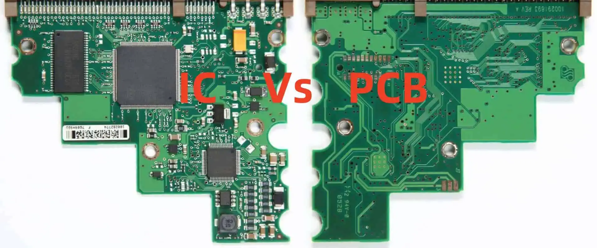
Integrated circuits (ICs) and printed circuit boards (PCBs) are both key components in modern electronics, but they serve different purposes. This article will explain what each one is, what they are made of, their role in an electronic system, and the key differences between the two.

What is an Integrated Circuit?

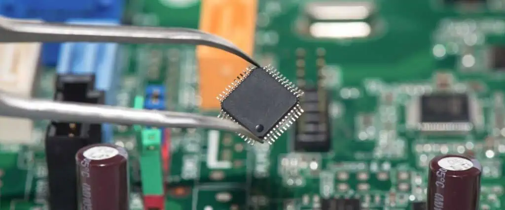
An integrated circuit, or IC, is a tiny silicon chip that can hold millions of microscopic electronic components like transistors, resistors, capacitors, and diodes. These components are etched onto the silicon through a fabrication process called photolithography.

ICs are essentially very complex electrical circuits with specific functions engraved on a single chip of semiconductor material. This โ€œintegratesโ€ many components into one package instead of using separate, discrete components wired together on a circuit board.

Common types of ICs include:

  • Microprocessors – The central processing units (CPUs) that serve as the โ€œbrainsโ€ of a system, performing calculations and executing program instructions
  • Memory chips – Data storage chips like ROM, RAM, flash memory
  • Microcontrollers – Mini self-contained computers with processor cores, memory, and programmable input/output
  • Analog circuits – Chips that process continuous analog signals vs discrete digital data
  • ASICs & FPGAs – Custom application-specific ICs and field programmable gate arrays

ICs go by many names, including chip, microchip, silicon chip, semiconductor device, or just chip. Their small size packs tremendous functionality and computing power into integrated, miniaturized circuitry.

What is a Printed Circuit Board?

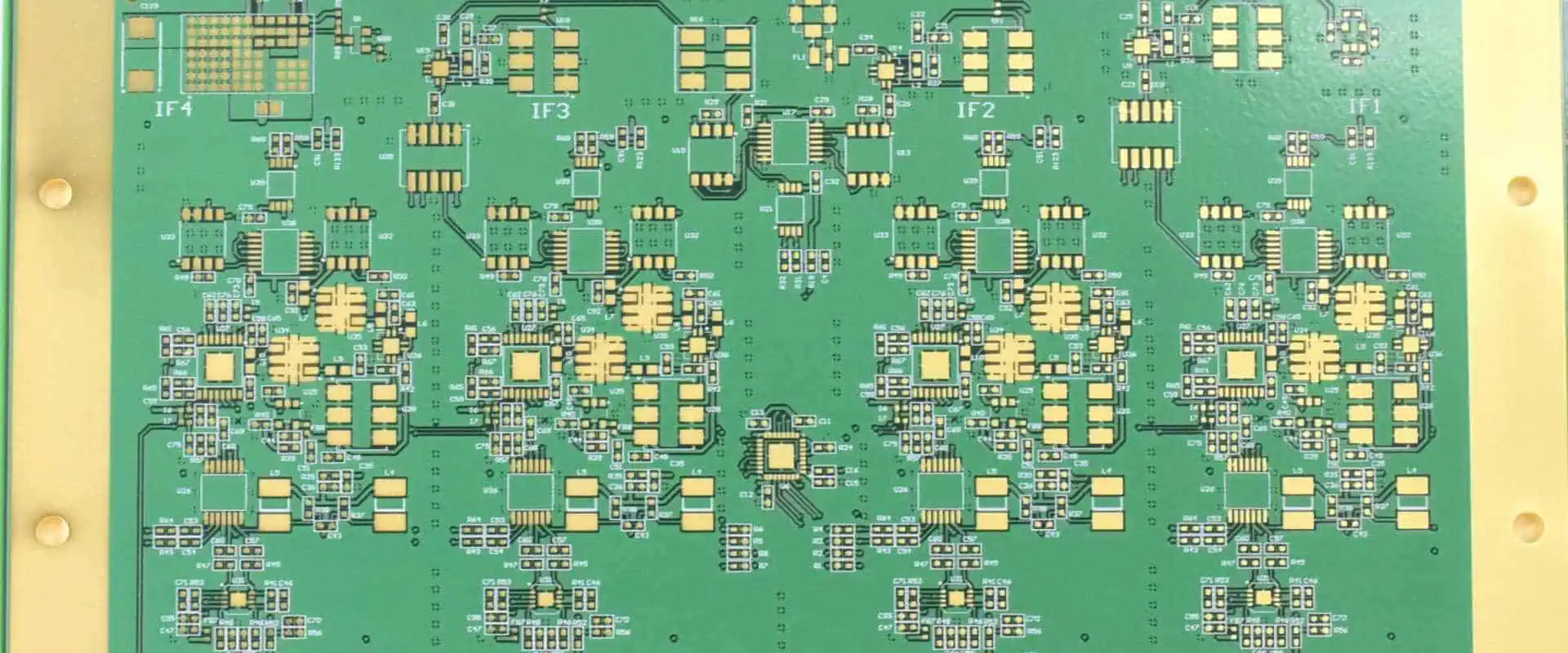
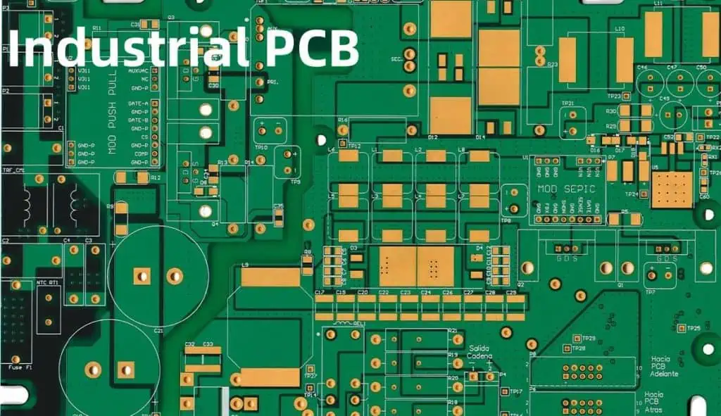
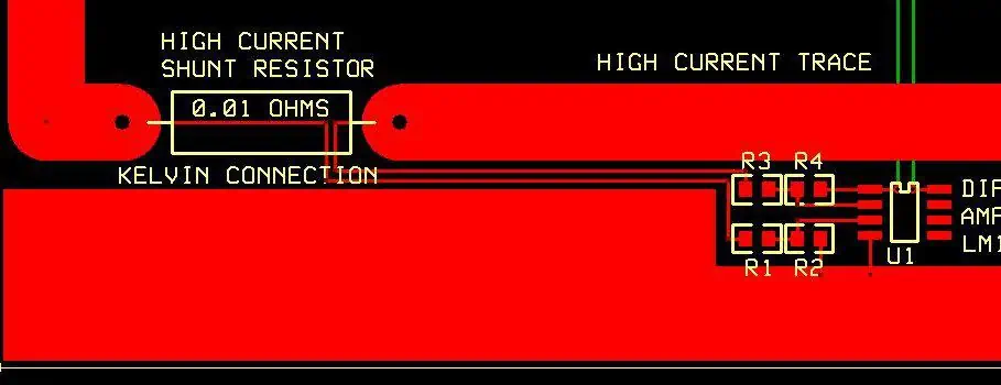
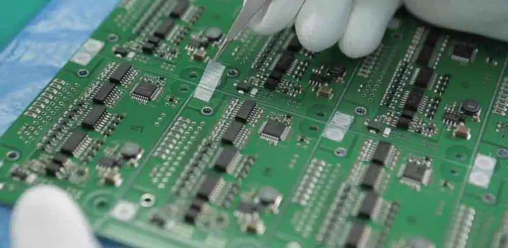
A printed circuit board (PCB) is a flat board made of insulating materials like FR-4 fiberglass onto which a โ€œprintedโ€ conducting copper circuit is layered and affixed. The circuit wiring patterns are etched from copper sheets and provide electrical connections between mounted electronic components in an organized manner.

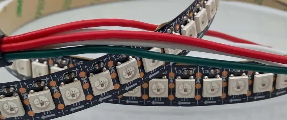
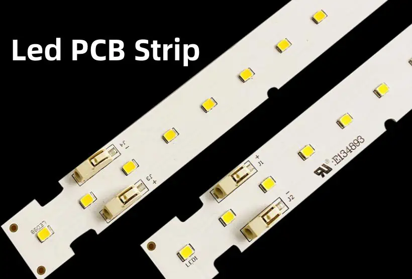
PCBs provide the mechanical framework to mount, connect, and integrate electronic components like ICs, resistors, capacitors, switches, connectors, batteries and more. They contain tiny copper tracks (wiring) leading to contact pads where component leads or connectors are soldered. Internal conductive layers and plated through holes connect tracks across layers.

In short, PCBs form the structural skeleton โ€œplatformโ€ to assemble electronics hardware, while ICs power the functionality.

PCB Composition vs IC Composition

PCB Embedded Components

PCBs and ICs vary significantly in their materials composition:

PCB Composition

  • Substrate – The base is an insulating material like fiberglass-reinforced epoxy laminate (FR-4)
  • Conductors – Copper foil sheets laminated onto substrate, etched to form wiring traces and pads
  • Dielectrics – Additional epoxy resin layers that insulate between conductor layers
  • Plating – Electroless nickel immersion gold (ENIG) coats exposed copper for soldering
  • Silkscreen – Epoxy ink prints component outlines and identifiers

IC Composition

  • Substrate – Pure monocrystalline silicon wafer base
  • Semiconductors – Doped silicon with specific electric properties
  • Dielectrics – Insulating silicon dioxide layers
  • Conductors – Embedded polysilicon or aluminum metal interconnects
  • Passivation Glass – Protective top glass layer

This table summarizes the key material differences:

MaterialsPrinted Circuit BoardsIntegrated Circuits
Base BoardPlastic composite like FR-4 fiberglassSilicon wafer
ConductorsCopper metal tracesPolysilicon interconnects
InsulatorsNon-conductive epoxy resinSilicon dioxide
CoatingsENIG over copper padsGlassivation passivation layer

The base substrate, wiring, and insulation materials differ significantly between PCBs and ICs due to differences in their manufacturing processes and functionality.

Manufacturing Process Comparison

PCBs and ICs are produced in very different factories using unrelated fabrication processes:

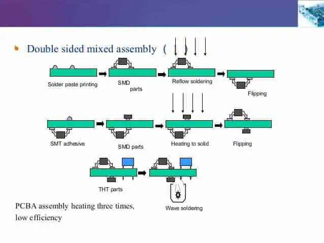
PCB Manufacturing Steps

  1. Design – PCB schematics and layouts are designed on EDA software
  2. Cleaning – The substrate starts with an oil removal clean
  3. Layer Stacking – Copper foil sheets are stacked up with substrate and prepreg
  4. Alignment & Lamination – Sheets are aligned and glued with heat and pressure
  5. Etching – Unwanted copper is chemically etched away
  6. Photolithography – Photoresist patterns and etches further define traces
  7. Plating & Coating – Exposed tracks are plated/coated with metals
  8. Solder mask – Epoxy layer insulates copper traces
  9. Silkscreen – Component outlines are printed
  10. Routing – Individual PCB panels are cut out
  11. Testing & Inspection – Quality assurance checks are performed

PCB fabrication leverages many industrial processes like automation, chemical processing, and precision tooling to produce completed boards.

IC Manufacturing Steps

The core IC fabrication takes place inside sophisticated semiconductor foundries or โ€œfabsโ€:

  1. Design – IC schematics and layouts designed on EDA software
  2. Fabrication – Raw silicon wafers are grown as base substrate
  3. Photolithiography – Ultraviolet light patterns microscopic transistor designs
  4. Etching – Chemical etching transfers the pattern to silicon
  5. Doping – Ions are implanted to alter electrical properties
  6. Layering – Conducting and insulating layers built up
  7. Annealing – High heat repairs crystal structure
  8. Bonding – Electrical probes attached to external pins
  9. Encapsulation – Mounted inside a protective housing
  10. Testing & Marking – Performance validated and marked

IC fabrication utilizes techniques from several advanced scientific disciplines like chemistry, physics, optics, nanotechnology, and material science.

This table highlights some processing differences:

manufacturing stepsPrinted Circuit BoardsIntegrated Circuits
Design ProcessPCB layout softwareIC modeling software
Layer GenerationMechanical laminationChemical deposition
Pattern TransferEtching, photolithographyPhotolithography, etching
Conductive TracesCopper metalPolysilicon, aluminum interconnect
Insulating LayersNon-conductive epoxySilicon dioxide
Size ScaleMillimeters to metersNanometers to micrometers

PCBs employ macroscale industrial techniques, while ICs leverage nanoscale semiconductor processes for microelectronics functionality.

Role & Function Comparison

Although their composition and fabrication vary greatly, ICs and PCBs work together symbiotically:

Integrated Circuits Role

ICs serve as the microchips powering computational functionality:

  • Processing – Execute software, perform calculations
  • Memory – Provide data storage and access
  • Connectivity – Enable system communication
  • Control Logic – Manage electrical systems
  • Safety Features – Monitor for errors and anomalies

This core โ€œbrainsโ€ logic comes etched right onto the silicon wafer material itself, packing maximum complexity into a tiny chip.

PCB Role

PCBs serve as the structural framework facilitating system assembly:

  • Interconnects – Copper traces link all mounted components
  • Platform – Rigid board physically supports parts
  • Alignment – Precise holes align inserting components
  • Cooling – Built-in heat sinks dissipate temperature
  • Protection – Shielding blocks electromagnetic interference

This โ€œbackboneโ€ architecture ties everything together into an integrated hardware system.

Key Differences Summary

ParameterIntegrated CircuitsPrinted Circuit Boards
DefinitionMiniaturized electronic computing components etched onto semiconductor materialComposite fiberglass boards providing structural base for circuit assembly
CompositionSilicon wafer substrate with embedded polysilicon interconnect circuitryFiberglass laminate with top and bottom layered copper foil conductors
RoleProvide core electronic functionality through precision integrated microcircuitryForm mechanical framework to mount, connect, and support electronic components
FabricationLayer-by-layer deposition of doped silicon, dielectrics and conductorsIndustrial processes of etching, coating, and lithography to shape substrate layers
End UseInstalled onto PCBs for functional deploymentHost ICs and other electronics parts integrated through copper wiring traces

In summary, ICs bring the complex electronic functionality that drives computation, while PCBs structurally support integration of these parts into complete working systems.

Frequently Asked Questions

rogers substrate

Here are answers to some common questions about ICs versus PCBs:

Q: Can an IC work without being mounted on a PCB?

A: No, ICs by themselves have no way to interconnect or physically mount inside a system. They must be appropriately placed and soldered onto PCBs to connect their input/output pins to copper wiring traces.

Q: Does a PCB have any function if no ICs are installed?

A: A plain PCB with only connectors brings little functionality. The ICs drive core digital processing, computation, memory, logic, and control capabilities to create an intelligent system.

Q: Which came first historically – PCBs or ICs?

A: PCBs originated from 1950s military electronics, while the first ICs emerged in 1961. So PCBs initially carried more discrete components until higher density ICs slowly got integrated over the 1960s and 70s.

Q: Can you implement an electronic product with just ICs or just a PCB?

A: No. All modern electronics require both complementary components. ICs provide function while PCBs enable integration, similar to organs and bones in the body.

Q: How are PCBs and ICs interconnected?

A: ICs packaging has metallic leads that get soldered onto matching copper contact pads on a PCB. This electrically and mechanically bonds them together through conductive solder alloy, enabling circuit connections.

Conclusion

Integrated circuits and printed circuit boards work hand-in-hand to enable all modern electronics. ICs integrate complex digital processing circuitry onto tiny silicon chips, which get structurally mounted onto the interconnect copper wiring traces of PCBs.

Understanding their distinct compositions, manufacturing processes, and functional roles is key to designing and assembling any electronic hardware product. Their synergistic partnership merges electronic functionality with an integration backbone into one powerful package.

So next time you look at an electronic device, recognize the critical symbiosis between precision integrated circuits energizing high-function silicon chips at the core, seamlessly enabling system integration through their attachment to flexible printed circuit boards!

IMI Sensors – Industrial Monitoring Instrumentation You Must Know

Industrial monitoring instrumentation (IMI) sensors play a crucial role in measuring and controlling processes across various industries. This article provides an overview of key IMI sensor types, applications, selection considerations, and frequently asked questions.

Temperature Sensors

Temperature measurement and control is critical for product quality, system performance, and safety. Common temperature sensor types include:

Thermocouples

Thermocouples contain two conductors made of different metals fused at one end. This junction produces a small voltage relative to temperature:

  • Inexpensive compared to other sensors
  • Wide temperature ranges up to 2300ยฐC
  • Low-cost options for fairly accurate temperature measurement
  • Available in different typesโ€”K, J, T, E, R, S, B, N

Resistance Temperature Detectors (RTDs)

RTDs contain a wire coil or film made of metals like platinum, copper or nickel. As temperature increases, electrical resistance increases linearly:

  • High accuracy with tight tolerance capability
  • Better repeatability and stability than thermocouples
  • Range capabilities from -200 ยฐC to 850 ยฐC
  • Common RTD typesโ€”Pt100, Pt1000, Ni120, Cu10

Thermistors

Thermistors contain semiconductor ceramics that alter resistance according to temperature fluctuation:

  • Inexpensive
  • Fast response times
  • Common as inrush current limiters and self-regulating heating elements
  • Can have high non-linearity requiring linearization

Table comparing different temperature sensor attributes:

SensorAccuracyRepeatabilityPriceResponse Time
ThermocoupleMediumMedium$Medium
RTDHighHigh$$Slow
ThermistorMedium/LowMedium$Fast

Infrared Thermometers

Infrared (IR) thermometers measure surface temperature from heat radiated without contact:

  • Non-contact temperature measurement
  • Capable of measuring moving surfaces
  • Prone to interference from external thermal influences
  • Typically offer fixed spot or line scanning

Integrated Circuit Sensors

Miniaturized integrated circuit sensors combine amplification, linearization, and temperature signal conditioning:

  • Built-in cold junction compensation for thermocouples
  • Linearized sensor output
  • Small physical size
  • Analog or digital output

Pressure Sensors

Pressure sensors measure and convert pressure forces into standardized electrical signals. Common types include:

Piezoelectric Pressure Sensors

Piezoelectric crystals produce proportional electrical charges under applied pressure:

  • For dynamic pressure measurement
  • Extreme precision and speed capabilities
  • Can only measure positive pressure change
  • Rugged and mechanical shock resistant construction
  • Bandwidths over 100 kHz

Capacitive Pressure Sensors

Use capacitive plates or diaphragms to detect pressure via dielectric medium deformation and capacitance change:

  • High sensitivty and accuracy potential
  • Expensive compared to other technologies
  • Capable of static and dynamic measurement
  • Vulnerable to high temperatures and shock/vibration damage

Strain Gauge Pressure Sensors

Detect pressure through deformation of strain gauges:

  • Most common pressure sensing technology
  • Low cost compared to others
  • Various pressure range capabilities
  • Difficult to protect from corrosion and moisture ingress

Piezoresistive Pressure Sensors

Piezoresistive elements alter conductive properties when mechanically stressed:

  • Low cost force and pressure sensing
  • Fast dynamic response times up to microseconds
  • Temperature sensitive requiring compensation
  • Vulnerable to damage from moisture and debris

Table comparing pressure sensor types:

SensorAccuracyBandwidthPriceRobustness
PiezoelectricHighestUp to 100 kHz$$$Excellent
CapacitiveHighUp to 10 kHz$$$Medium
Strain GaugeMediumUp to 1 kHz$Medium
PiezoresistiveMediumUp to 20+ kHz$$Low

Level Sensors

Level sensors measure and monitor liquids and other materials within a container or vessel. Models include:

Float Switches

A float containing magnets rises/falls with liquid level to activate a reed switch:

  • Inexpensive
  • Simple setup
  • Prone to scale buildup and debris fouling

Capacitive Level

Detects liquid level changes through capacitance measurement instead of physical contact:

  • No moving parts
  • Resistant to vibrations and pressure fluctuations
  • Difficult mounting through existing vessel tops

Differential Pressure

Infers level based on measured differences in hydrostatic pressure:

  • Simple electronic design
  • Low cost compared to other technologies
  • Requires impulse piping to liquid vessel
  • Subject to clogging

Ultrasonic Level

Uses reflected sound waves to determine liquid level and volume:

  • Works on various liquid types
  • Unaffected by electrical conductivity
  • Top-mounted for easy access and visibility
  • Expensive compared to other options

Guided Wave Radar

Propagates low-frequency radar wave through probe into liquid:

  • High accuracy and precision measurement
  • Capable in extreme pressure/temp applications
  • Difficult calibration and temperature compensation
  • Generally the most expensive solution

Table showing key attributes of level sensor technologies:

SensorAccuracyLocationMaintenancePrice
Float SwitchMediumInside vesselHigh$
CapacitiveHighOutside vesselLow$$
Differential PressureMediumOutside vesselMedium$$
UltrasonicHighAbove vesselLow$$$
Guided Wave RadarHighestInside vesselMedium$$$$

Flow Sensors

Flow sensors analyze, measure, and monitor flowing liquids, air, steam or gases. Instruments include:

Differential Pressure

Measure flow rate based on energy loss across an orifice plate:

  • Low capital cost and simple operation
  • Works across diverse fluids and pipe scales
  • Orifice plates prone to fouling and clogging

Magnetic Flow Meters

Use electromagnetic principles to measure conductive fluid velocities:

  • High accuracy and excellent repeatability
  • No moving parts or orifice constrictions
  • Only works on electrically conductive liquids

Coriolis Flow Meters

Precisely track mass flow using resonance frequencies in vibrating flow tubes:

  • Direct mass flow measurement capabilities
  • High accuracy and rangeability
  • Generally one of the most expensive technologies

Ultrasonic Flow Meters

Leverage Doppler shifts in ultrasonic waves reflecting through liquid:

  • High accuracy and repeatability
  • Bi-directional flow measurement
  • Requires particulates for wave reflection
  • Typically costly compared to other options

Vortex Flow Meters

Generate and measure fluid vortices for volumetric flow indication:

  • No moving parts or obstructions
  • Good accuracy across wide velocity ranges
  • Performance impacted by low flow velocities
  • Unable to measure mass flow

Comparison of key flow sensor attributes:

SensorAccuracyRangeabilityPriceRobustness
Differential PressureMedium10:1 typical$Excellent
MagneticHigh100:1+$$$Very Good
CoriolisHighest100:1+$$$$Limited
UltrasonicHigh50:1+$$$Good
VortexGood20:1+$$Very Good

Gas Detection Sensors

Gas monitoring is vital for safety, emissions control, and process optimization. Instruments include:

Infrared Gas Sensors

Leverage infrared light absorption characteristics of target gases:

  • Available for most common toxic gases
  • Typically very sensitive and stable
  • Can have interference issues in dirty environments

Electrochemical Gas Sensors

Use electrode reactions to quantitatively indicate target gases:

  • Offer ppm sensitivity levels
  • Simple and inexpensive
  • Prone to poisoning/contamination failure

Metal Oxide Semiconductor (MOS) Sensors

Alter conductive states based on reactions with oxidizing/reducing gases:

  • Respond to wide variety of reactive gases
  • Operate well at high temperatures
  • Lack specificity between gas types
  • Lifespans limited by operational duty cycles

Photoionization Detectors (PID)

Ionize chemical gases using ultraviolet light for detection:

  • Respond to diverse VOCs
  • Sub-ppm sensitivity
  • Unable to differentiate specific compounds
  • Require periodic UV lamp replacement

Catalytic Bead Sensors

Detect combustible gases via combustion on electrically heated pellistors:

  • Wide rangeability can reach 100% LEL
  • Low purchase and operating costs
  • Lack specificity between gas types

Table summarizing instrumentation for gas detection:

SensorRangeAccuracyPriceSelectivity
Infrared0-100% LELVery High$$Excellent
Electrochemicalppm levelsHigh$Good
Metal Oxideppm levelsMedium$Poor
Photoionizationppb-ppmHigh$$Medium
Catalytic Bead0-100% LELMedium$Poor

Process Analytical Instruments

Process analyzers provide real-time quantification of liquid/gas chemistries:

PH Instrumentation

PH measurement is critical for monitoring water quality, reactor processes, and biological processes. Options include:

  • Electrochemical electrodes – common for inline industrial measurement
  • Litmus paper – inexpensive spot sampling
  • Digital benchtop/handheld meters – laboratory analysis

PH control instrumentation includes chemical metering pumps, solenoid valves, and databases of automated dosing control algorithms.

Conductivity Measurement

Conductivity cells quantify ion concentrations within process liquids. This can identify:

  • Impurities in water feeds
  • Chemical reaction progression
  • Alkalinity and other water chemistry

Typical instrumentation incorporates contactless toroidal sensors or diagnostic tables for identifying specific chemical components based on conductivity.

Gas Chromatographs

Gas chromatographs utilize separation columns and compositional analysis to identify gas mixtures. Applications involve:

  • Natural gas, fuel, and feedstock purity
  • Quantifying levels of contaminants
  • Monitoring chemical reaction progress

Chromatographs offer excellent analytical precision but require skilled personnel for calibration and data interpretation.

Spectrophotometers

Spectrophotometric analyzers pass specific wavelengths of light through samples to quantify absorption characteristics. This identifies:

  • Chemical reaction completion
  • Presence of unsaturated organics and compounds
  • Component concentrations in mixtures

IMI Sensor Selection Considerations

Proper IMI sensor selection, installation, wiring, and maintenance ensures optimal performance. Considerations include:

Measurement Properties

  • Required engineering units and process ranges
  • Necessary accuracy and precision
  • Expected process variable dynamics

Environmental Factors

  • Process media types and conditions
  • Ambient temps, pressures, vibration
  • Exposure to moisture, debris, corrosion

Infrastructure Integration

  • Electrical outputs, communication interfacing
  • Physical footprint limitations
  • Mounting provisions, remote capabilities

Operational Realities

  • Maintenance access and intervals
  • Recalibration and replacement needs
  • Operator skill level and preferences

Budget Constraints

  • Initial capital outlay acceptable
  • Recurring ownership costs over lifetime
  • Installation, civil, and secondary infrastructure

Frequently Asked Questions

What are the different kinds of transmitters for IMI sensors?

Common transmitter outputs include 4-20 mA analog, HART digital communication, WirelessHART, Foundation Fieldbus, Profibus PA, and modular plug-in universal designs. This provides connectivity to control systems like PLCs and DCS platforms.

How do you install RTD temperature sensors?

RTD sensors require precise immersion depth control and thermal grease/compound to ensure proper heat transfer contact. 3 or 4-wire configurations compensate for lead resistance. Match sheath materials to environmental media compatibility.

How do I prevent corrosion failure in pressure sensors?

Choose compatible wetted parts materials for process fluids. Use chemical seals/diaphragms. Control fluid velocity/turbulence at sensor connections. Avoid fluid ingress through proper mounting orientation. Consider corrosion resistant coatings and surface treatments.

What flow sensors work with dirty liquids?

Differential pressure instruments tolerate considerable solids contamination when properly designed. Magnetic flow meters lack flow obstructions enabling particulate passage. Coriolis meters dynamically flex flow tubes to prevent accumulation when measuring slurries.

How often should gas detectors be calibrated?

Electrochemical and infrared sensor performance drifts over 6-12 month intervals depending on environmental factors and pollutant exposure. Recommended gas detector calibration frequency ranges from monthly to annually. Always adhere to manufacturer guidance for recalibration and replacement intervals.

What is Industrial PCB? ( Design and Manufacturing Standards)

Industrial printed circuit boards (PCBs) refer to boards designed to operate reliably in demanding environmental conditions for extended time periods, usually 5-10+ years. They enable core functions for products used in sectors like transportation, energy, automation, aerospace and defense.

Unlike commercial grade boards, industrial PCBs face punishing temperature swings, shock, vibration, humidity and other challenges. They require rigorous design, component selection and testing well beyond typical electronics. In this guide, we explain what defines industrial PCBs and overview key design and manufacturing standards driving longer lasting, rugged boards.

Defining Industrial PCBs

Industrial PCBs differentiate on:

Operating Environments – Made for extreme industrial settings with wider temperature (-40ยฐC to 105+ยฐC), shock/vibration, humidity and other environmental demands.

Lifespan – Designed for high reliability over long product field life, often 10-15+ years of near continuous operations.

Criticality – High availability, functionality and safety criticality if the PCB fails. Whole industrial systems may rely on them.

Some examples of electronics using specially designed industrial class PCBs include:

  • Motor drives
  • Industrial controllers
  • Power supplies
  • Battery chargers
  • Process transmitters
  • Remote terminal units
  • Railway electronics
  • Downhole drilling tools
  • Aerospace avionics
  • Military vehicle electronics

Ruggedness, extended lifespan and high reliability distinguish industrial PCBs even though they may resemble commercial boards upon visual inspection. Their unique constraints lead to various design and manufacturing rules.

Industrial PCB Design Standards

Engineers designing industrial printed circuit boards face various international standards prescribing construction methods, documentation models, risk analysis techniques, testing procedures and key metrics to achieve longer field life over temperature extremes, vibrations and fast transients.

Some of the major standards include:

IPC Class 3

Issued under IPC-2221 standards, it covers generic performance requirements for industrial electronics printed boards especially related to:

  • Temperature cycling (-65ยฐC to 150ยฐC)
  • Vibration (10-500Hz at 10G+)
  • Mechanical shock of 100-1500G
  • Moisture resistance
  • Other environmental stresses

Additionally covers recommended test methods, quality conformance criteria and inspection details useful for qualifying Class 3 boards. It represents a minimum level for most industrial applications.

IPC-6012 Automotive Electronics

Includes performance standards tailored for automotive/transportation use cases covering details like:

  • Temperature ranges (-40ยฐC to +125ยฐC )
  • Rapid humidity transitions
  • Vibration profiles
  • Test schedules
  • Inspection criteria
  • Qualification maintenance

Contains Class 1, 2, 3 acceptance levels (Class 3 most demanding)

IPC-A-610 Acceptability Standard

Visual defect criteria focused on workmanship, component orientation, soldering, part types and surface finishes. Used globally across PCB types to determine quality through manufacturing and acceptance inspection. All boards should pass IPC-A-610 for ship readiness.

IEC-61188 Circuit Boards

International guidelines from IEC on:

  • Printed board layout and stackup
  • Material/finish properties
  • Electrical test methods
  • Environmental stress testing
  • Lot traceability through production

Of note for industrial boards are temperature/humidity cycling, mixed flowing gas corrosion testing and chemical resistance outlined.

UL 796 Standard for Printed-Wiring Boards

Underwriters Laboratory standard including various flame resistance, temperature indexing tests, electrical testing and constructions methods for boards.

Special UL 796 File Number recognition requires passing a range of safety focused design evaluations applicable to boards used in the UL safety certification ecosystem. Useful for boards used in end-products seeking UL listing especially for power electronics.

Industrial PCB Materials and Constructions

To withstand higher stress, industrial PCBs utilize additional materials and stackup methods:

Substrates

Material Properties Applications
FR-4 Glass Epoxy Low cost, moderate performance Mild environments
High Tg FR-4 Increased heat resistance Power electronics
Polyimide Extreme temperature range Downhole, space, aviation
IMS Thermal conductivity LEDs, power devices
Ceramic High frequency, temperature RF/microwave, harsh
Metal Core Heat dissipation Power, LED

Special Layers

  • Extra thick copper (>2 oz.) for currents
  • Impedance control layers
  • Buried/blind vias for HDI
  • Flood/plane layers for EMI shielding
  • Graphite layers aid thermal heat spreading
  • Double sided boards for shock/vibe damping

Coatings

  • Conformal coating – moisture, contamination and corrosion resistance
  • Potting compounds – vibration, thermal shock resistance

Edge Plating Connectors

Reinforced gold or tin-lead edge connector fingers withstand 10K+ mating cycles.

Industrial PCB Design Practices

Design is crucial for reliable functionality under demanding conditions:

Simulation Early – Extensive electrical, thermal, vibration modeling using tools like Ansys or Comsol to predict response and resonances. Spot problems ahead of building prototypes pcb.

Derating Rules – Component derating guidelines lowering actual operating values below datasheet absolute maximums for voltage, current and power. Provides margin against parameter drift and lifespan reduction.

Redundancy – Extra backup pathways, traces, connections with automated failover capability. Prevents single points of failure.

Layout Methods – Thermal management techniques, stitching vias, edge control structures and wide, thick conductors to handle vibration, currents.

DFMx Analysis – Rigorous design analysis checks for manufacturability issues around thermal relief connections, trace widths, annular rings and more.

Standards Validation – Testing conformity with defense standards like MIL-PRF-31032 or those above helps qualify designs.

Getting board layout right from the start avoids costly re-spins later so taking the time to simulate, analyze and standard-proof industrial PCB designs is well worth it.

Industrial PCB Manufacturing and Testing

Producing industrial PCBs uses tighter process controls, auditing and qualification procedures than commercial boards:

Software – MES, ERP, MRP help coordinate workflow, Machine interfaces aid automated optical inspection and test

Fab – Cleanrooms, 6 sigma process controls on 35+ fabrication steps including pattern plating.

TestICT finds shorts and opens. Flying probe checks nodes. AOI inspects defects. X-ray confirms inner layer detail.

QA – Full traceability on materials and processes. Conflict minerals reporting required. Factory audited to AS9100, ISO 9001

Qualification – IPC Class 3 certification, UL E-file safety approval after verification testing during new product introduction and then sustained through periodic re-qualification

Personnel – Operators undergo certified training on accepting boards to IPC-A-610 visual standards reliably

Data Packs – Full archive packs for each board with photomicrographs, electrical test results,Corrective action reports from any issues detected during manufacturing or test

This combination of precision digital manufacturing technology paired with quality framework helps yield the reliable, long lasting circuit boards needed in industrial situations.

Choosing an Industrial PCB Partner

Given the unique demands of industrial PCBs, partner selection matters greatly:

Look for

  • Years of experience specifically with industrial customers
  • Wide material expertise like ceramic, IMS, flex-rigid and metal core PCBs
  • Design for Excellence services aiding product development
  • Staff engineers that can validate layouts to standards
  • Global quality certifications – ISO, AS9100

Ask About

  • Handling of proprietary customer data and red team reviews
  • DFM optimization methods and GERBER analysis
  • Standard testing and inspection processes
  • Qualification reports provided
  • Inventory and obsolescence management programs
  • Counterfeit part avoidance controls

This best equips product teams to accelerate robust, compliant printed circuit board designs optimized to survive longterm in the real world conditions faced.

Conclusion

Industrial electronics have special PCB reliability requirements well beyond commercial boards to perform properly for years across extreme environments and safety critical applications.

By designing to rigorous standards upfront through simulation, analysis, derating and redundancy while choosing a tightly controlled, certified PCB factory, companies can meet their customersโ€™ expectations in the harshest use cases. The specialized materials, testing and qualification processes for industrial PCBs delivers confidence for successful field deployment.

Frequently Asked Questions

What are some example applications using industrial class PCBs?

Typical applications leveraging industrial printed circuit boards include transportation power systems, factory automation controllers, energy management products, remote telemetry units, military vehicle computing, aerospace avionics, downhole drilling tools, naval systems and similar electronics where high reliability over 5-15+ years is necessary.

How are industrial PCBs different than commercial PCBs?

Industrial PCBs differentiate by:

  • Supporting wider operating temperatures (-65ยฐC to +150ยฐC)
  • Longer field deployment lifetimes (10-20 years)
  • Required survival through harsh vibration, shock, moisture conditions
  • High availability and uptime (>99%)
  • Rigorous product testing and qualification
  • Precision manufacturing process controls
  • Traceability documentation Which exceeds commercial PCB environmental and lifespan demands.

What are some ways engineers design industrial PCB layouts differently?

Design techniques used for industrial printed circuit boards include:

  • Component derating below absolute maximum levels
  • Thermal simulation using finite element models
  • Redundant connections and pathways
  • Vibration damping edge mount connectors
  • Conformal coating for moisture protection
  • Thicker power and ground traces
  • Double sided boards to withstand shock
  • Extensive DFM analysis before release

Why is FR-4 still commonly used if industrial PCBs face extreme temperatures?

While special substrates like polyimides and ceramics handle wider temperature swings, FR-4 laminates have evolved โ€œhigh Tgโ€ versions usable to 150ยฐC+ along with lower cost and better fabricator familiarity. So FR-4 remains an option for many industrial applications not hitting extreme temps.

What certifications should we look for in an industrial PCB manufacturer?

Key quality certifications to require from a factory producing printed circuit boards destined for industrial products include:

  • ISO-9001-2015 – Quality management systems
  • AS-9100D/EN9100 – Aerospace standard with strict guidelines
  • ANSI/ESD S20.20 – Control of electronics ESD hazards
  • ISO 14001:2015 Environmental Management
  • IATF 16949 – Automotive quality management
  • ITAR registration – Required for defense/aerospace PCBs
  • IPC validated – For fabrication to IPC standards

These demonstrate the necessary capabilities to manufacture reliable boards over years of field deployment.

What is Route keepin and Rounte Keepout in PCB?

Route keepin and keepout are critical concepts in printed circuit board (PCB) design that refer to deliberately routing traces through or avoiding certain regions to meet layout guidelines and electrical requirements.

Route keepin defines areas where the PCB router must pass signal traces to force connectivity with components placed in that zone.

Route keepout conversely defines excluded regions that traces must avoid routing through to prevent interference or maintain spacing from nearby components.

Understanding keepin and keepout methodologies is essential to optimizing PCB routing and minimizing signal quality issues or fabrication defects.

Key Differences Between Route Keepin and Route Keepout

Route keepin and keepout share some similaries but have distinct definitions and implementation:

Route KeepinRoute Keepout
DefinitionArea where traces must pass throughArea where traces must avoid
PurposeEnsure trace connectivityPrevent signal interference
SpecifiesMandatory trace routingForbidden trace routing
Failure ModeOpens, disrupted connectionsShort circuits, crosstalk

Types of Route Keepin

Several key types of route keepin exist with different connectivity objectives:

Component Pin Keepin

Forces connectivity between component pins and the remainder of the circuit. Ensures no open circuits during routing.

Power Plane Thermal Connection

Guarantees power pins route to a thermal pad or copper pour to dissipate heat.

Stitching Vias Keepin

Makes routing pass through periodic vias to stitch together different layer planes. Maintains proper return paths.

Faraday Cage Keepin

Routes traces through shielding cages around noise sensitive circuitry to maintain isolation.

Mechanical Outline Keepin

Routes critical traces along the physical PCB extents to enable edge mount connectors.

Types of Route Keepout

Various key route keepout regions also exist:

Silkscreen Keepout

Avoids placing traces under annotations to prevent visibility issues after fabrication.

Copper Pour Keepout

Prevents traces from entering copper fill areas to avoid accidental bridging due to etching defects.

Electrical Clearance Keepout

Ensures separation between traces and adjacent pads/traces meets target clearance rules to prevent short circuits.

Mechanical Drill Keepout

Keeps traces clearing away from mechanically drilled PCB holes to account for potential drill wandering during fabrication.

Test Points Keepout

Allows space for temporary test point accesses around points of interest for debug probing without blocking trace routability.

Implementing Keepin and Keepout in PCB Layout

PCB layout tools provide both manual and automated methods to assign route keepin and keepout:

Manual Assignment

The designer manually draws required keepin/keepout shapes and configures rules forcing or blocking traces from entering each area. Allows precision control but can be time consuming.

Component-Driven Automation

Software automation dynamically generates mandated trace access or exclusion areas based on placed component pin locations, pad geometry, and electrical settings like net classes. More efficient but with less customization.

Manufacturing-Driven Standards

Many fabricators provide standard design rule check (DRC) constraint files that designer tools leverage to auto-assign generic keepin/keepout regions. Facilitates ease-of-fabrication but with conservative assumptions.

Benefits of Implementing Thoughtful Keepin and Keepout

Intelligent use of route keepin and keepout delivers major PCB optimization including:

1. Ensures Critical Trace Connectivity

Forcing traces through certain areas guarantees nodes that must be electrically tied together connect during routing without reliance on designer effort to pre-route.

2. Reduces Signal Integrity Issues

Separating sensitive nets using pin/trace exclusion regions enables cleaner routing with less undesired coupling that degrades signal performance.

3. Optimizes Manufacturability

Guiding traces to required locations and away from high-risk zones proactively mitigates potential fabrication defects through prevention.

4. Facilitates Debugging

Strategic channel creation permits test probes access during bring-up labs while isolation barriers prevent probe grounding issues.

Impact of Keepin/Keepout Misconfiguration Hazards

While powerful capabilities, incorrect keepin/keepout implementations risk major consequences:

Excessive Route Blockage

Over-constraining areas that traces must avoid can block all viable routing paths resulting in incomplete trace connections.

Signal Performance Degradation

Allowing sensitive traces to occupy noise-coupled regions without proper isolation degrades signal spectral purity, eye diagrams, jitter, and bit error rates.

Fabrication Defect Generation

Permitting traces into zones with insufficient electrical or mechanical spacing guarantees at least localized short circuits and potential panel scrapping.

Test Access Limitations

Lack of test point regions can prevent affirming critical internal nodes leading to extensive debug efforts when integration issues emerge.

PCB Examples Using Effective Keepin and Keepout

Several case study examples highlight practical applications of intelligently leveraged keepin/keepout:

Example 1: DDR Memory Routing

DDR nets utilize pin keepin and excluded zones around vias enforcing controlled impedance paths between memory controller and modules guaranteeing timing margin.

Example 2: USB 3.0 Channel Routing

Paired differential USB traces maintain 100 ohm differential impedance routing through layer transitions using keepin while ground fills provide shielding isolation.

Example 3: BGA Fanout Routing

Dense BGA fanout traces achieve required spacing passing between bumps by assigning narrow routing channels using electrical clearance keepouts on each side.

Example 4: RF Transceiver

A transceiver utilizes perimeter stitching vias keepin combined with an interior copper pour keepout to define RF cage shielding isolating the noise-sensitive functionality.

Conclusion

In summary, PCB route keepin and keepout deliver necessary capabilities balancing connection enforcement versus isolation avoidance that together enable optimized layouts meeting stringent signal integrity and manufacturing compatibility needs. As PCB technologies and performance requirements scale in complexity, mastery over keepin and keepout confers a significant competitive advantage ensuring design success.

Frequently Asked Questions

What happens if too much route keepout is defined on a complex design?

Excessive keepout can overconstrain the routing problem space and block all viable connectivity paths between points that must be electrically connected. This prevents the design from being routable.

How are route keepins for differential pair routing implemented?

Differential trace pairs leverage keepins to force pairing through matched impedance paths. The keepin shapes match the spaced trace widths and are just larger than the nominal spacing gap to guarantee maintaining proper differential impedance.

Can both keepins and keepouts overlap in the same physical board area?

Yes, keepins and keepouts can coexist in certain scenarios. For example, a keepin may force a trace to route through a region but avoid encroaching on adjacent keepout zones separation sensitive circuitry nearby.

What reference design resources provide good keepin/keepout examples?

Many semiconductor vendors supply reference PCB layouts illustrating recommended keepin/keepout usage for interfaces like DDR, PCIe, USB3, HDMI, and other standards-based connectivity. These serve as excellent implementation examples.

What are some key pitfalls when validating keepin/keepout correctness?

Engineers should carefully confirm keepin/keepout rules do not overlap or contradict. Additionally, sufficient margin to facilitate fabrication tolerance and provide available space for routing is vital. Tight overconstraint frequently causes issues.

What is a Kelvin connection PCB?

A Kelvin connection refers to a four-wire electrical measurement configuration used to determine the precise resistance of a device under test (DUT) with high accuracy. Kelvin connection printed circuit boards (PCBs) integrate this specialized wiring pattern into the PCB traces to enable accurate on-board resistance measurement of components.

In a Kelvin connection, two wires are used to source current through the DUT while a separate two wires sense the resultant voltage drop. This eliminates errors caused by wiring resistance to achieve micro-ohm precision unmatched by traditional two-wire (non-Kelvin) connections.

Why Use Kelvin Connections on PCBs?

There are several benefits to integrating Kelvin connections into a PCB design:

Precision Current Shunt Resistance Measurement

High-power PCBs often incorporate current shunts – low value resistors designed to measure current flowing through a circuit. Kelvin connections on the shunt traces allow micro-ohm resolution that improves current measurement accuracy.

Accurate Sensing of Voltage Drops

Minimizing trace resistance allows small voltage drops across PCB nodes to be sensed with less noise using Kelvin connections. This helps calibrate power regulation circuits.

Analyze PCB Copper Integrity

Measuring PCB trace resistances during quality control verifies design integrity and detects defects like cracks or gaps. Kelvin connections provide repeatable precision trace measurements.

Improved Reliability Testing

Monitoring PCB trace resistance changes using Kelvin connections during temperature or vibration testing correlates small damage before outright failure.

Key Properties of Kelvin Connections

To enable accurate resistance measurement, Kelvin connections exhibit:

1. Electrically Isolated Current and Sense Traces

Separate pairs of traces are used to source current and measure voltage. No current flows through the sense traces.

2. Low Impedance Paths

Thicker, short traces minimize parasitic resistance allowing micro-ohm resolution.

3. Direct Component Terminations

Sense traces connect directly across the resistive component, not indirectly through a node.

4. Optional Shielding

Shielding prevents noise coupling from high current flow into precise sense traces.

##Types of Kelvin Connection Implementation

Several approaches exist to integrate Kelvin connections into PCBs:

Discrete Wired Resistors

Discrete surface mount or through-hole resistors are soldered to dedicated Kelvin termination pads connected by wide traces.

Printed Resistive Elements

Thick-film or etched copper elements patterned directly on the PCB surface act as shunt resistors with Kelvin connections.

Internal Layer Traces

Entire internal copper layers are devoted to low-impedance Kelvin wiring to minimize trace lengths throughout a multilayer PCB stackup.

High Density Kelvin Arrays

Arrays of spring-loaded contact pins allow temporary connections to pads on boards under test for production line automated testing.

ImplementationProsCons
Discrete ResistorsInexpensive, interchangeableLarger footprint, lower precision, slower measurement
Printed ResistorsCompact size, higher precisionCustom fabrication required
Internal Layer TracesExcellent measurement resolutionComplex PCB design, high layer count
High Density ArraysAutomated testing, custom grid pitchesExpensive fabrication, fragile pins

Kelvin Connection Considerations for PCB Design

Several key guidelines should be followed when laying out Kelvin connections in circuit boards:

1. Minimize Trace Lengths

Keep all 4 traces as short and wide as possible to reduce parasitic resistances.

2. Avoid Trace Bends/Shapes

Refrain from trace angles or shapes which increase impedance through the thin circuit board laminate.

3. Use Copper Fills for Shielding

Adding copper fill shapes connected to ground around the traces shields noise sources.

4. Include Test Points

Test points allow temporary connections to the internal PCB Kelvin wiring to facilitate debugging or failure analysis.

Applications and Usage Examples

Kelvin connection PCB implementations enable precise resistance measurement across a variety of applications:

Power Supply Current Monitoring

Shunt resistors with 4-wire Kelvin connections provide temperature stable, high-resolution current sensing for closed-loop supply regulation.

Battery Pack Wired Resistance Measurement

Cell balancing circuits in battery packs leverage Kelvin connections to measure wiring harness resistances influencing voltage accuracy.

Press Fit Connector Contact Resistance Testing

Measuring contact resistance changes in press-fit PCB connectors during thermal cycling qualifies reliability using mayn dedicated Kelvin connection spring pins.

Continuous PCB Trace Integrity Testing

Running high current loads while continuously monitoring copper trace resistances with Kolvin connections over long time periods assesses reliability.

Biomedical Sensor Calibration

On-board Kelvin wiring allows micro-ohm resolution tuning and calibration of delicate instrumentation amplifier circuits used in medical sensors.

Conclusion

Integrating Kelvin connections into printed circuit board designs enables accurate resistance measurement unachievable by traditional two-wire configurations. By isolating current flow and voltage sense pathways both electrically and physically, noise is reduced achieving micro-ohm precision critical for precision current monitoring, voltage drop sensing, and PCB copper integrity validation. With thoughtful layout and shielding, PCBs with Kelvin connections populate a diversity of applications ranging from power electronics to biomedical instruments.

Frequently Asked Questions

How does a Kelvin connection provide more accurate resistance measurement compared to traditional wiring?

Kelvin connections eliminate the measurement uncertainty caused by parasitic resistance in the wires used to source current by providing a separate isolated pair to sense voltage with ultra low-impedance. This avoids measurement error.

What magnitude of resistances can be measured with Kelvin connected PCBs?

Properly designed Kelvin connections allow resistances from milliohms down to microohms to be resolved. This covers measurement of typical current sense elements, PCB traces, and other integrated resistive components.

Does the thickness and length of the traces impact Kelvin connection performance?

Yes, using shorter and thicker copper traces is critical to minimize trace resistances below the micro-ohm devices under test. Long, thin traces degrade resolution through excessive trace resistance and noise pickup.

How many wires does a Kelvin connection require?

Four wires are needed – two distinct connections to each terminal of the resistive device under test. This provides dedicated current flow and voltage sense pathways to avoid measurement errors.

Can Kelvin connections adjust for temperature drifts during resistance measurement?

Yes, by using temperature calibration standards with known resistance drift specifications and similarly constructing the DUT, temperature induced resistance changes can be accurately measured with the Kelvin connection.

What is Keyboard PCB Tester?

A keyboard PCB tester is a device used to test the functionality and connectivity of a printed circuit board (PCB) designed for a computer keyboard. Keyboard PCB testers allow manufacturers and hobbyists to validate all aspects of a keyboard PCB design before assembling the final keyboard.

Keyboard PCB testers verify the following functions:

  • Electrical connectivity between switches, microcontrollers, and other PCB components
  • Switch matrix scanning operation
  • MIDI/audio output signal generation
  • Compatibility with keyboard firmware
  • Full N-key rollover (NKRO) capability

Why Use a Keyboard PCB Tester?

There are several key benefits to using a keyboard PCB tester during the design and manufacturing process:

Validate PCB Trace Integrity

The PCB tester can validate that all intended electrical connections have been properly etched into the PCB during fabrication. This ensures no broken or partial traces exist on the board that would prevent correct switch matrix scanning.

Reduce Costly Re-spins

By fully testing a keyboard PCB before production, any design flaws can be identified early. This avoids costly PCB re-spins later in the development cycle.

Verify Firmware Compatibility

Testing the PCB with keyboard firmware loaded confirms the microcontroller chip can properly interface with the PCB hardware. Incompatibilities can be addressed in either the PCB or firmware.

Check N-Key Rollover Capability

Keyboard testers enable validating that no ghosting issues occur, even when many keys are pressed simultaneously. This confirms the keyboard matrix can support full NKRO operation.

Streamline Manufacturing Testing

Performing comprehensive tests with a keyboard PCB tester means less testing is needed later during production. This saves manufacturing time and cost.

What to Look for in a Keyboard PCB Tester

There are several key factors to evaluate when selecting a keyboard PCB tester:

Switch Matrix Test Interface

The tester should provide an interface to mount the keyboard PCB and connect switches installed in each position of the switch matrix. This allows scanning of the complete matrix.

Matrix Size Number of Switches
60% ~60
75% ~80
80% ~85
100% / Full 100-110

Integrated Keycap Simulators

High-quality testers come with physical key actuators to simulate key presses. These can validate the sensor/switch mechanism and provide a realistic typing feel.

MIDI and Audio Output

Test MIDI and audio output generation from the keyboard PCB by connecting to external speakers or a Digital Audio Workstation (DAW).

Firmware Loading Capability

There should be a method to load the keyboard’s firmware onto the microcontroller to test full functionality and compatibility.

NKRO Testing Features

Advanced testers provide specialized interfaces to press multiple switches simultaneously. This confirms the keyboard matrix and firmware supports full NKRO.

Multimeter Probes

Some testers integrate digital multimeter probes to measure continuity, resistance, capacitance, and voltage of PCB components and traces during testing.

Debugging Interfaces

Interfaces like JTAG or SWD allow advanced debugging of the keyboard microcontroller firmware and low-level operation.

Types of Keyboard PCB Test Solutions

There are a variety of keyboard PCB test solutions available depending on application requirements and budget.

Custom Test Fixtures

Fixtures consist of an array of mechanical switches mounted to a baseplate to interface with the keyboard PCB switches and simulate key presses. Custom fixturing provides flexibility to accommodate different PCB sizes but requires fabrication expertise.

Universal Testers

Universal keyboard testers feature an adjustable housing to adapt to different PCB sizes. They integrate keycap simulators, MIDI/Audio validation tools, and debugging features into a single device. These provide excellent functionality but at a high cost.

Popular universal testers include:

  • GoKey Tester
  • SO Layer Electronic Keyboard Tester

DIY Testing Stations

Hobbyists often create custom testing devices using DIY electronics kits or prototyping boards like Arduino or Raspberry Pi. These low-cost platforms can interface with keyboard matrices to validate basic functionality but require significant development effort.

Performing Tests with a Keyboard PCB Tester

The general workflow for testing a keyboard PCB consists of:

1. Mount the PCB

Secure the keyboard PCB into the tester interface with the switch positions properly aligned.

2. Install Firmware

If testing with firmware, load the keyboard firmware hex file onto the microcontroller.

3. Connect Power

Connect the appropriate power source to turn on the keyboard PCB. USB or battery power are typical.

4. Actuate Switches

Manually press buttons on the integrated keycap simulators or external keyboard to actuate each switch position.

5. Validate Matrix Scanning

Monitor the keyboard protocol data using debug software to validate the firmware detects each switch actuation.

6. Test MIDI/Audio Output

If MIDI/Audio features are supported, validate correct waveform generation by connecting speakers or MIDI recording software.

7. Validate NKRO

Using a specialized NKRO interface, press an array of keys simultaneously to confirm no ghosting or blocking occurs.

8. Debug Issues

Use integrated tools like multimeter probes or debugging interfaces to diagnose and fix issues with traces, solder joints, components, or firmware.

Application Examples of Keyboard PCB Test Fixtures

Keyboard PCB testers enable a wide range of applications during design, pre-production, and manufacturing:

Research & Development

Engineers use keyboard test fixtures during R&D to validate PCB designs iteratively without needing complete prototypes.

Design Verification

Quality engineers can formally verify all acceptance criteria are met for connectivity, scanning, rollover, and output generation using detailed test procedures.

Production Line Testing

Streamlined validation procedures with keyboard PCB testers during manufacturing reduce the overhead of quality control processes.

Safety & Compliance

Testing helps certify each keyboard PCB meets electrostatic standards or is compliant with electrical safety regulations for the target market.

Partner/Supplier Qualification

Brands qualifying PCB or electronic component vendors utilize testing to ensure suppliers meet quality benchmarks.

Fault Diagnosis & Repair

Hobbyists and repair technicians leverage DIY keyboard testers to efficiently troubleshoot issues with non-functional keyboards.

Conclusion

Corne keyboard PCB
Corne keyboard PCB

Keyboard PCB testers enable validation of all functional aspects of a keyboard PCB design before assembling the final keyboard enclosure and keycaps. By thoroughly testing the bare PCB, manufacturers can identify issues early and reduce costly re-spins later in the process. From simple custom test fixtures to advanced universal solutions, there are tester configurations available for any application need and budget. As keyboards become increasingly complex, keyboard PCB test instrumentation will continue growing as an essential tool for design, pre-production verification, manufacturing, and service workflows.

Frequently Asked Questions

What are the key functions tested by a keyboard PCB tester?

The main functions validated by keyboard PCB testers include: electrical connectivity between PCB components, switch matrix scanning operation, MIDI/audio signal generation, firmware compatibility, and N-key rollover capability.

When in the design flow are keyboard PCB testers used?

Keyboard PCB testers are primarily used to validate designs after fabrication of the bare PCB and before enclosure assembly. This enables issues to be identified early before large production runs occur.

What interface is used to actuate the PCB switches during testing?

Most universal keyboard PCB testers utilize physical actuators to press each switch on the board and simulate key presses. Custom test fixtures generally interface bare switches to mechanically activate the PCB switch sites.

Can hobbyists create their own keyboard testing devices?

Yes, hobbyists can construct custom DIY keyboard test devices using kits based on platforms like Arduino or Raspberry Pi. These low-cost tools allow basic validation but require significant development work.

How are multiple simultaneous key presses tested to validate NKRO ?

Advanced commercial keyboard PCB testers come equipped with specialized interfaces to allow pressing large arrays of keys at once. Signals can then be monitored to check no ghosting or blocking occurs during extreme conditions.

How to Add Multiple PCBs in one KiCad Project

KiCad EDA suite is a powerful open-source electronics design automation platform enabling professionals and hobbyists alike to take electronic systems from concept to final routed PCB layout.

A major advantage of using KiCad over some commercial EDA tools is it allows including multiple PCB configurations within the same project design.

This is beneficial when dealing with complex designs requiring several inter-dependent circuit boards or versions to fully implement the target electronics hardware end-product.

This article provides a step-by-step walkthrough on how to correctly structure and manage multi-board KiCad projects, leveraging inheritance relationships to maximize design reuse. Screenshots demonstrate the key steps involved.

Follow along to learn how to efficiently architect complex multi-PCB solutions as one Master Project in KiCad.

Multi-Board Project Scenarios

Some typical use cases where designing several PCBs as part of consolidated project in KiCad makes sense:

  • Main Board + Daughter Boards – Eg. CPU board + display board combinations with interconnection through high density connectors
  • Board Sets – Devices involving panels/racks with duplicate PCBs plugged into backplane bus structure
  • Versions/Derivatives – Spinning off variants like HW version 1.0, 1.1, 1.2 of base design
  • Master/Slave System – One primary controller PCB with additional peripheral PCBs

In above cases, instead of managing each PCB layout completely independently in isolated KiCad projects, you can define linkage and inheritance relationships between boards early on during the design phase. This allows propagation of changes across dependent boards later avoiding painful rework.

Let’s see how step-by-step.

Configuring Multi-Board Project Structure

The first step is to configure the project structure to accommodate multiple boards belonging to same overall system design. This sets you up to achieve maximum re-use and consistency across individual PCBs due to centralized configuration inheritance reducing duplication or variation by error through project life cycle.

Start Fresh New Project

Launch KiCad and select File > New Project > New Project

Pick any folder location to host the Master Project. This will hold all the individual PCBs and common data.

Create “Project Level” Schematic Folder

Click Add Existing Folder to Current Project toolbar button showing green icon with “plus” symbol.

Browse to folder projectname just created and select subfolder path:

Copy code

projectname/-schematics

This establishes main /-schematics folder for holding any common schematic documents used across ALL boards like power or interface definitions.

Generate Each Board#X Schematic Sheet

Still under the Common Schematic Folder path in left tree view, now create respective schematic document for EACH planned PCB layout board.

Right click mouse, select Create New Schematic

Do this sequentially to initialize first sheet schematic file individually for however many boards intended in full project scope.

Eg. For 4 PCBs:

  • board1.sch
  • board2.sch
  • board3.sch
  • board4.sch

schematic sheets now created ready for circuit drawing later for each planned board.

Next Complete PCBnew Configurations

Repeat the same process now instead under the main project root to initialize corresponding .kicad_pcb layout file for each board schematic created already

Eg. For 4 PCBs:

  • board1.kicad_pcb
  • board2.kicad_pcb
  • board3.kicad_pcb
  • board4.kicad_pcb

These .kicad_pcb files inside root will become respective PCB layout containers related to each schematic sheet after netlist import.

This table summarizes the multi-board project folder structure and file types configured:

LocationFile TypeDescription
/project/schematics.schCommon Schematic Sheets
/project/.kicad_pcbIndividual PCB Layout

We now have framework ready to start actual PCB design work!

PCB Circuit Schematic Design Stage

With blank schematic sheets created ready per board, we can begin capturing actual circuits and connectivity. Standard workflow applies just like single board project.

It helps conceptually dividing schematics as:

  • Common Circuits – Schematics logic used by multiple boards eg. power input filtering section
  • Base Circuits – Baseline schematics sections reused by derivative boards via inheritance
  • Unique Circuits – Schematics logic only applying to that specific board

This distinction helps manage change control between shared versus child schematic sheets when alterations occur later down the development timeline.

Follow standard schematic capture best practices as well creating logical schematic architecture for each PCB through combination of:

  • Part symbols from installed component libraries
  • Bus lines to reduce complexity
  • Hierarchical structure using sub-sheets to simplify
  • Net and wire labeling
  • Design rule checks to validate integrity of connections

Cross Probe Between Schematics

Use the KiCad Cross-probing toolbar icon showing magnifying glass symbol to quickly navigate across sheets to trace wires connections between schematics as complexity builds up.

Output Schematic Netlists

Upon finishing respective board’s schematic sheets design work, next output netlist connectivity file. Repeat this process individually for each board’s schematics.

Steps:

  1. Open respective .sch schematic sheet
  2. Tools > Generate Netlist > PCBNew Netlist
  3. Save netlist as eg. board1.net for each board
  4. Repeat generating one netlist per board in project

Netlists act as bridge linking logical schematic connectivity to physical PCB layout.

PCB Layout Routing Stage

With connectivity netlists files now available board-wise, we can focus attention to converting schematics into routed PCB.

Again standard workflow applies – initialize board sizes, import netlist, assign footprints, run ERC, place components, route traces until completion for EACH board independently.

However, some additional considerations working on complex multi-board projects include:

Cross Probing Between Layouts

Use the same Cross-Probe toolbar button to quickly navigate between layouts by clicking pushpin marker to understand connectivity spanning across boards.

Inheritance Concept

Leverage inheritance relationships early instead of duplicating similar circuits or networks again. Eg. Common power supply section from one layout can propagate to other boards via cross-probing rather than redrawing.

Validate Across Boards

Before finalizing layouts, cross-validate that schemes used for connectors, mounting holes, silkscreen artworks are consistent across boards which will eventually interface during system assembly stage downstream.

Final Manufacturing Output Handoff

Upon completing all PCB layouts routing and checks, last step is generating manufacturing CAM outputs – Gerbers, NC Drills, Assembly drawings etc. – needed to fabricate the bare boards with a PCB supplier.

Again same process done earlier for single board projects applies here.

Some pointers when submitting manufacturing gerber data for quotation:

  • Send separate zip folders per PCB for clarity even though single project
  • Use consistent file naming conventions indicating parent project
  • Include precise bare board fabrication and solder masking requirements
  • Provide accurate target quantities needed for each board reflecting overall system build volumes

This completes end-to-end design process to realize complex electronics systems made up of multiple PCBs configurations managed efficiently as one Master Project in KiCad EDA tool.

FAQs

What is the best folder structure for multi-board KiCad project?

Below folder architecture allows clean separation between common and board-specific logical assets when dealing with multi-PCB project:

/-projectname

  • /schematics (common schematic sheets)
    • power.sch
    • busdef.sch
  • /board1
    • board1_schematic.sch
    • board1.kicad_pcb
  • /board2
    • board2_schematic.sch
    • board2.kicad_pcb

So keep shared documents in parent level folders while individual PCB data under respective child folder.

How do I check differences between PCB layouts in multi-board project?

When iterating on designs with multiple boards, it helps cross-validate differences between board Layout versions.

KiCad provides built-in layout comparative functionality:

  1. Open first board layout .kicad_pcb
  2. Select menu Tools > Compare PCB Layouts
  3. Browse and select second .kicad_pcb layout design
  4. Adjust ignore thresholds if needed under various comparison criteria

This does smart diff analysis reporting differences between layouts helping synchronize changes across dependent boards.

Can I split complex schematic across multiple sheets for cleanliness?

Yes, when working with multi-page schematics for big designs, instead of cramping up all logic into giant single sheet canvas, apply divide and conquer approach:

  • Break down by functional modules
  • Use hierarchical sheets and ports
  • Cross link between sheets using invisible nets
  • Show external connectivity through block symbols

This reduces scrolling needs and aids readability helping focus on specific logic section when making edits instead of getting overwhelmed viewing entire schematic complexity on one page.

Cross-probing facilitates navigation while ERC checks validate connections consistency between fragmented schematic sheets. Page index table helps map document structure when interfacing design reviews. So fully utilize tools at disposal to creatively architect complex schematics refinement modularly across multiple sheets using KiCad’s versatile EDA environment capabilities.

I hope this gives a good starting point for electronics designers to efficiently structure KiCad projects involving multiple PCB layouts instead of struggling managing disconnected documents. Follow the principled approach touching on configuration, re-use via inheritance, cross-validation between boards and version control to yield productivity benefits when dealing with high complexity multi-board system solutions as one Master Project.

How do I convert a Schematic to PCB Layout in KiCad (Step By Step)

KiCad is a free, open source electronics design automation suite for Windows, Mac, and Linux, widely used by hobbyists, makers, and engineers to design printed circuit boards (PCBs).

Converting your KiCad schematic to PCB layout is an essential step in the process of designing a custom PCB, allowing you to define the physical board and component layout matching your circuit schematic connectivity.

This article provides a step-by-step workflow to successfully move from schematic capture to populated PCB layout using KiCad version 5.1.9’s schematic and PCB editor tools. Screenshots illustrate the key steps.

Let’s get started!

YouTube video

KiCad Design Flow Basics

Below are the basic work stages as you move from concept to finished PCB manufacturing file output when using the KiCad EDA tool suite:

  1. Schematic Capture – Draw circuit diagram connecting components with nets
  2. Schematic Symbols Creation – Make new parts with unique symbols and footprints
  3. Schematic Annotations – Assign reference designators to parts
  4. Netlist Generation – Output connectivity netlist file (.net)
  5. Footprint Assignment – Associate footprints to schematic parts
  6. Design Rule Check – Validate schematic for ERC/DRC errors
  7. PCB Layout – Convert netlist to board with parts placed and routed
  8. Gerber File Generation – Manufacturing output from PCB

We will focus specifically on steps 4 to 7 which enable progression from completed schematic diagram to functional PCB layout, ready for fabrication.

Generate Netlist File From Schematic

Schematic Design in KiCAD

Once your schematic circuit drawing in the KiCad Eeschema schematic editor is logically complete with part symbols wired by nets representing connectivity just like the circuit should operate in physical reality, we are ready to move from schematic to board layout.

The NETLIST file acts as the bridge between the schematic sheet components connectivity and the layout board definition.

To generate a netlist:

  1. Select menu Tools > Generate Netlist Files
  2. Select the checkbox for format Pcbnew (*.net)
  3. Enter filename test_board for the netlist
  4. Select checkbox option Generate single net for unconnected pins
  5. Click OK button

This will generate test_board.net file with net connectivity data matching your schematic diagram’s circuit logic.

The key output netlist formats from Eeschema used at different points in the PCB design process are:

Netlist FormatDescription
.netPCBNew format used for PCB layout routing
.xmlPCBNew format used to import custom schematic footprints
.bomBill of Materials format for assembly

For now, we need the .net PCBNew netlist file that has extracted nets and component connectivity intelligence from the schematic.

Time to move to the PCB Layout editor.

Import Netlist into PCBNew Layout Tool

The PCB Layout editor tool within KiCad is named Pcbnew. This is the canvas where we will map our schematic circuit’s logical connectivity defined graphically in Eeschema down onto the physical domain of the PCB board that will be manufactured.

To import the generated netlist file:

  1. Launch Pcbnew from the KiCad toolbar
  2. Go to menu File > Import Netlist
  3. A dialog prompts you to select the *.net netlist file previously created.
  4. Select the checkbox option Keep Existing Libraries
  5. Click OK

This will open up the main PCB layout canvas and import all the parts and nets defined in our source schematic, ready for board layout work.

Run Electrical Rules Check

Before rushing into board layout placement and routing, it is good practice to run an electrical rules check on the imported netlist to spot any violations with component pin mappings or missing connections compared to the schematic.

Go to top toolbar Tools > Electrical Rules Check

KiCad will analyze the entire netlist and schematic connectivity, flagging warnings if finds any:

  • Unresolved component pin numbers conflicts when mapping schematic symbols to PCB footprints
  • Missing connections / continuity issues versus the schematic sheet
  • Duplicate reference designators assigned
  • Etc.

Address any errors or warnings reported at this stage before further progressing the design conversion. Once ERC passes cleanly, we can be confident to continue with component placement and layout work confident that the PCB connectivity matches the schematic completely.

Assign PCB Footprints to Components

Setting Footprints
Setting Footprints

Every schematic symbol needs a matching PCB footprint assigned, which defines the physical land pattern on the board matching how component terminals will eventually solder down.

To assign footprints:

  1. With PCB board open, select menu Tools > Assign Footprints
  2. A spreadsheet loads with list of all schematic parts.
  3. Choose matching PCB footprint required from libraries already installed for each part.
  4. Saved selections automatically get mapped.

Repeat for all components ensuring every part has both:

  • Unique schematic symbol in schematic editor
  • Corresponding PCB footprint in Pcbnew layout tool

This cross-mapping connects the gates and pins of abstract schematic symbols to real solderable terminations on board.

PCB Layout Design Setup

Before placement and routing, some initial PCB layout design rule and workspace configurations need defining first:

  • Board outline dimensions
  • Copper layer counts
  • Grid & Component clearance rules
  • Net classes for trace widths/clearances
  • Routing zones definition
  • Layer stack table

Tools under Design Rules and Preferences menus allow correctly pre-setting these parameters matching circuit needs and capabilities of your PCB fabrication process.

For a simple single-sided PCB:

  • Define rectangular board dimensions under Page Settings
  • Add Keepout layer graphical boundary showing max size
  • Set 50mil grid spacing under Preferences
  • Define clearance rules between tracks, pads, vias
  • Map layers to physical PCB fabrication layers

Default settings tables can be used initially and refined later once placement is underway.

Begin Component Placement

We can now start intelligently placing components on the PCB canvas to gradually transform from rats nest to routed board layout matching schematic.

Steps for component placement:

  1. Select component to place from list of imported parts from schematic
  2. Move crosshair cursor to desired location on board
  3. Click or tap to anchor component at chosen position.
  4. Orient part footprint by R key rotation if needed
  5. Repeat placing all parts onto board canvas

Tips for good placement practices:

  • Follow logical grouping – Eg. place together related resistors, caps, ICs etc.
  • Start placing parts from a fixed reference like one board corner
  • Place parts from large to small size
  • Watch spacing – provide room for traces between parts
  • Think ahead for track routing paths
  • Place parts on front layer first then back layer

There are no fixed placement rules – experiment until parts layout passes visual sanity check ensuring adequate spacing while following natural circuit zones matching schematic flow.

Use grid snap and zoom controls to fine tune component locations as you work through placing the imported parts list.

Interactive Routing of Component Connections

F-Component Routing Techniques

Having all parts dropped means we now need to connect the dots – to make tracks linking parts pins together as electrically defined by our netlist connectivity imported from the schematic. This is the routing stage.

To interactively route:

  1. Select signal layer intended for trace
  2. Choose routing tool – track/via/wire
  3. Click trace start point – say a component pad
  4. Route trace and click destination pad
  5. Repeat tracing all points in same signal net

Routing Tips

  • Minimize via counts on signal layers
  • Use angled traces instead of meanders
  • Complete power traces first then signals
  • Route one trace end to end before starting next trace
  • Think neatness – avoid chaotic board appearance.

Use grid and snap controls to tidy up traces. Switch layers when changing routing direction avoiding collisions. Toggle rats nest view to verify unrouted connections pending.

The goal is to effectively link component pads together using copper track traces layer by layer until the rats nest fully disappears.

Your routed board should perfectly mirror the schematic connectivity down to the physical domain once routing is complete.

Final Checks – DRC, 3D View, Emulate

Before generating manufacturing gerber and drill files, run final checks:

  1. Design Rule Check – Validate no clearance violations under menu Tools > Design Rule Check
  2. 3D View – Under View > 3D Viewer visually check for missed connections in 3D mode
  3. Emulate – Tool Tools > Generate Footprint Positions File exports a .pos 3D assembly file from the board to mechanically trial component fit, clearances etc. in a New Project

Fix any last minute minor issues based on the feedback from these validation checks.

Output Gerber and Drill Files

Finally, we are ready to produce manufacturing outputs by plotting gerber masks and drill hits database.

Steps:

  1. Menu File > Fabrication Outputs.
  2. Select All layers you want outputs for- Top copper, bottom copper etc.
  3. Ensure options to generate Drill Map (.drl) file is selected.
  4. Click Make Plots button to save gerber files.

Send the Gerber zip file bundle with .drl drill map to your PCB fabrication vendor’s order upload portal or rep to get your designed bare boards manufactured now!

Final Words

kicad-schematic

And that concludes converting a KiCad schematic drawing down to functional PCB layout ready for fabrication and assembly.

The key concepts covered again:

  • Generate netlist connectivity file from schematic capture
  • Import this into new PCBnew layout project
  • Assign footprints matching schematic symbols
  • Follow methodical placement and routing workflow
  • Complete design rule checks before output
  • Export manufacturing plot gerber and drill data

As you gain proficiency translating schematic circuits to routed boards using the KiCad open source EDA tool suite, your custom PCB realization confidence and speed only gets better through applying these fundamentals incrementally to build experience.

Hope this gives electronics hobbyists, makers and engineers a helpful starter framework to take first concept schematics through to manufacturable layout output systematically using the popular KiCad platform.

Good luck with your next schematic to PCB layout project!

FAQs

What are some key hotkeys useful for PCB Layout in KiCad?

General Navigation

  • mm – Move origin crosshair
  • Jump – Rapidly move canvas to selected object
  • < > – Flip Board
  • a – Select layer/tool/settings
  • z – Dynamic zoom
  • g – Toggle grid visibility

Layers & Colors

  • l – Flip current layer
  • Shift+S – Stack colors
  • ./, – Next/previous layer

Editing Actions

  • m – Move footprint
  • r – Rotate footprint
  • f – Flip footprint
  • Del – Delete item

Trace Routing

  • x – Route track segment
  • v – Place via
  • Shift – Cycle through available widths
  • . , – Cycles displayed nets

Consult full KiCad PCB hotkeys list for all shortcuts available.

What’s a good work flow for routing a complex board in KiCad?

For a complex board with high component density and tight clearance requirements, here is an efficient professional routing workflow to follow:

1) Have power input section already defined
2) Place any shield can components first establishing space
3) Grid place groups of same-function parts (ICs, caps etc)
4) Route power buses first on inner layers first
5) Fanout traces from each group keeping same nets together
6) Complete high-speed traces first, minimize vias 7) Use grid to tidy up traces layout iteration by iteration
8) Do most routing on outer layers keeping inner organized
9) Treat every trace uniquely, don’t batch all connects
10) Continually DRC check; validate 3D view for sound assembly

Following the above methodical placement-routing sequence minimizes chaos, rework and ensures optimal board layout quality from complexity perspective.

How do I calculate trace widths in KiCad to handle required current loads?

You can either manually calculate appropriate copper trace widths on PCB to safely carry expected current using factors like:

  • Conductor temperature rise
  • Base copper thickness
  • Maximum current expected
  • Ambient temperature considerations

Or simply leverage KiCad’s intuitive built-in PCB calculator to compute minimum widths and spacing.

Steps to use KiCad Trace Width Calculator:

  1. After placement work, select Menu Tools > Calculator
  2. Go to tab PCB Trace Width
  3. Enter variables like Current, Temperature Rise, Copper Weight
  4. See minimum Trace Width value calculated

This helps quickly validate trace geometries planned are adequately sized to handle power rails current, preventing overheating while being cost effective not over-designing.

What should I do if changes happen to the schematic after routing is complete?

It is common in complex board design that logic modifications or component shuffling happens in schematic even after substantial layout routing has occurred. KiCad has some smart ways to forward-migrate changes:

  • For minor component reference designator alterations, use Swap Reference tool under Tools > Reference menu to rapidly remap parts
  • For modest connectivity changes, manually edit routed traces to match revised nets
  • For major schematic changes, scrap existing work and go back to start – regenerate netlist from new schematic version and re-import to wipe slate clean!

So depending on scope magnitude of ECO changes to base schematic, you can either surgically update final layouts or restart conversion process to resample schematic. Use version control between major iterations.

I hope these additional tips help further demystify practical aspects converting schematic concepts to physical PCB layouts using the KiCad EDA open source software suite.

RoHS Compliant Lead Free PCB Assembly Services in China: The Ultimate FAQ Guide

smt pcb assembly machinesmt pcb assembly machine

What is a RoHS Compliant Lead-Free PCB Assembly?

RoHS compliant lead free printed circuit board (PCB) assembly refers to a circuit board assembly manufactured using lead free solder and components that comply with RoHS (Restriction of Hazardous Substances) standards and regulations.

RoHS is a European Union regulation that restricts the use of 6 hazardous substances in electrical and electronic equipment:

  1. Lead (Pb)
  2. Mercury (Hg)
  3. Cadmium (Cd)
  4. Hexavalent chromium (Cr6+)
  5. Polybrominated biphenyls (PBB)
  6. Polybrominated diphenyl ether (PBDE)

A lead free PCB assembly uses lead free solders such as tin-silver-copper (SAC) alloys rather than traditional tin-lead solder. Lead free PCB assemblies also use electronic components that meet RoHS requirements for maximum concentration values tolerated for the 6 restricted substances.

Benefits of Lead Free PCB Assembly

Some key benefits of using RoHS compliant lead free PCB assemblies include:

  • Environmentally Friendlyย – Reduces hazardous e-waste and exposure of toxic substances to humans and the environment
  • Regulatory Complianceย – Meets RoHS and other global environmental regulation requirements for electronics
  • High Reliabilityย – Lead free solders can offer comparable or even better reliability than tin-lead
  • Easier Recycling and Reuseย – Due to lack of hazardous substances in assembly components

Many electronics manufacturers worldwide now require RoHS and lead free PCB board assembly for their products. Consumer demand for greener electronics is also driving adoption of lead free soldering process and components. For these reasons, PCB assembly service providers in China are moving towards sustainable manufacturing processes for global customers.

Why Choose China for Lead Free PCB Assembly?

China has emerged as the electronics and PCB manufacturing hub powering the world’s consumer electronics industry. Here are some of the key benefits of lead free PCB assembly services in China:

1. Cost Savings

China provides very competitive pricing for RoHS compliant and lead free PCB assemblies for export markets while still delivering quality. Manufacturing and labor costs are lower.

2. Production Capacity

High volume SMT assembly lines optimized for efficiency and scale. Able to handle fluctuating customer demand and production ramps.

3. Specialized Knowledge and Equipment

Chinese EMS companies continuously invest in the people, equipment, technology needed to assemble lead free PCBs, meeting latest quality and RoHS standards.

4. Supply Chain Advantage

Easy access to abundant Component sources and suppliers in China to mitigate electronic component shortages and lead times for customers globally.

With both capabilities and capacity for cost effective and compliant lead-free PCB assembly, China has become the go-to manufacturing base servicing a large percentage of global electronics OEMs including many American and European brands.

Key Parts in a Lead Free PCB Assembly

A lead free PCB assembly has three key components:

1. Lead Free Printed Circuit Board (PCB)

This refers to the bare PCB fabrication made of laminates, copper traces, and components pads/footprints using RoHS compliant materials and processes. Common substrates used are FR-4 and CEM-3.

2. Lead Free Components

This includes active and passive surface mount device (SMD) components used on the PCB that meet RoHS maximum concentration values tolerated for the six restricted substances according to IEC 62321 standard.

Some examples:

  • Integrated circuits (ICs)
  • Semiconductors
  • Resistors, capacitors
  • Transistors, diodes
  • LEDs, relays
  • Connectors

3. Lead-Free Solder

Lead-free solders replace conventional tin/lead solder to make solder connections between pads on the PCB and component termination finishes.

Common lead-free solder alloys used:

  • Tin Silver Copper (SAC) alloy: SnAgCu
  • Tin Copper (SACX): SnCu

Below is a breakdown comparison between conventional tin/lead solder characteristics versus lead-free SAC solder alloy commonly used:

Characteristic Tin/Lead Solder Lead Free SAC Solder Alloy
Melting Point 183ยฐC 217ยฐC to 220ยฐC
Wettability Good Moderate to good
Solderability Good Good
Electrical Conductivity Excellent Good
Mechanical Properties Good Good
Creep Resistance Fair Excellent
Fatigue Life Good Good
Thermal Cycling Good Good

As the comparison table shows, the lead free SAC solder alloy offers comparable and even better performance than conventional tin/lead solder in some characteristics such as creep resistance while maintaining complete RoHS compliance.

Manufacturing Process for Lead-Free PCB Assembly

double sided pcb assembly process

The basic manufacturing workflow to assemble RoHS compliant lead free PCBs involves two main processes:

1. SMT (Surface Mount Technology) Assembly

This is assembly of surface mount device (SMD) components onto the PCB using lead free soldering techniques. The key steps are:

  1. Solder Paste Screen Printing – Lead free solder paste stencil is used to apply precise amounts of solder paste onto PCB pads
  2. SMD Component Placement – Use of high speed Pick and Place machines to accurately place tiny chip components onto PCB pads
  3. Solder Reflow – SMD components attached by passing PCB loaded with components through a reflow oven heating to melt solder paste and forming solder joints

2. Wave Soldering or Manual Soldering (for Through Hole components if any)

This second stage is for attachment of any leaded through hole (TH) components by:

  1. Wave Soldering – Passing the PCB bottom side through a molten lead free solder wave to solder leads into plated through holes.
  2. Manual Soldering – specialist operators use lead free solder wire and iron to hand solder leads

These two core assembly processes with RoHS compliant materials, when executed with extreme precision using well-tuned assembly lines, modern equipment, and strict process controls allows the manufacturer to deliver high yielding and reliable lead-free circuit board assemblies cost effectively in China.

Below illustrates a simplified sequence for manufacturing RoHS compliant and lead free PCB assemblies in China:

Quality Control and Assurance such as visual inspection, AOI, x-Ray, ICT testing is interwoven between manufacturing processes to verify assembly quality against defects.

Guide to Cost Factors for Lead Free PCB Assembly in China

What are the key cost drivers when estimating and comparing lead free PCB assembly quotes between Chinese electronic manufacturers? Below is an overview:

a) PCB Parameters

  • PCB Class – Class 2, Class 3 PCB or higher have more layer counts impacting complexity
  • PCB Size
  • Copper thickness – 1 oz., 2 oz. or thicker copper PCBs
  • Gold finger connectors – Expensive material addition
  • V-cuts or special routing – Add additional fabrication costs
  • Panel utilization – Batch PCB quantity being assembled for optimal efficiency
  • PCB quantities and potential volumes

b) Component Parameter

  • SMD component sizes – 0201, 0603, 1206 etc. The smaller, the harder and costlier it is to handle and assemble
  • SMD component counts – total number of placements
  • Complexity of bill of materials (BOMs) – total number of component/item line items
  • High pin count SMDs – can be challenging to solder or re-work
  • Number of BGAs or other special package components requiring x-ray inspection
  • Total component placement value
  • Component lead time and inventory overhead – for hard-to-source parts

c) Other Materials

  • Solder paste – Some special solder wire or solder paste adds cost
  • Adhesives or encapsulation epoxy – for protecting certain components

d) Secondary Operations

Secondary PCB assembly operations that could impact cost:

  • Cleaning
  • Conformal coating
  • Programming or loading firmware/software
  • Testing requirements and coverage beyond standard practice
  • Box build with enclosure/cables
  • Custom labeling, logo printing

e) Service Factors

Service parameters that add a premium:

  • Low or fluctuating volume – increases down-time and changeover costs
  • Expedited or “jump the queue” lead times below capability
  • Documentation overhead – more process control plans required
  • Extra production monitoring required – live video feeds
  • High mix, slow ramp BOM and engineering change management
  • Excess handling due to fragile boards or packaging requirements

By accurately accounting for above factors that incur additional material, process, quality or service costs, the manufacturer can provide realistic assembly pricing. Lead-free assembly in China balancing performance, quality, and fair cost then becomes very achievable.

FAQ – Lead Free PCB Assembly in China

Below are answers to some frequently asked questions foreign OEM customers have regarding outsourcing RoHS compliant and lead free electronics manufacturing to Chinese EMS suppliers.

Can you ensure RoHS compliance for PCB assembly in China? How?

Yes, any established mid to large size PCB assembly house in China supplying to export markets can guarantee RoHS compliance today. Here is why and how they achieve this:

1) Updated Equipment and Solder
They invest in new soldering systems, storage and handling that can enable lead-free manufacturing separating from tin/lead solder equipment.

2) Material and Component Controls
Strict receiving inspection and test procedures ensure only RoHS certified materials and pre-approved electronic components are used in production meeting IEC 62321max concentration requirements.

3) Process Controls and Operator Training
Soldering process window adjustments to account for higher melting point temperatures. Training on handling and storage of lead free solder paste and materials.

4) Compliance Verification
XRF material chemistry analysis and IPC testing validates RoHS thresholds ensuring no cross-contamination through adequate flushing during product transitions.

Taken together, these hardware, process, people and compliance measures ensure PCB deliverables comply with RoHS and other environmental directives for global customers.

Are there any reliability issues with lead free solder joint integrity? How is this addressed?

Lead free solder alloys in particular SAC 305 used today have well established excellent thermal cycling reliability comparable to tin/lead joints for standard PCB assembly.

However, for high reliability or thermal sensitive applications, there may still remain certain concerns to address:

  1. SAC Solder Joint Brittlenessย Use of SAC305 with addition of alloying elements like Ni, Bi, In, and Ce can enhance ductility, fracture resistance and anti-cracking capabilities.
  2. Intermetallic Compound (IMC) Formation
    Optimizing reflow profile peak temperatures between 240ยฐC to 260ยฐC and minimizing time above 217ยฐC can help restrict excessive IMC growth maintaining a strong but thin enough Cu-Sn IMC interface.
  3. Mechanical Drop Shock or Vibration Resistance
    Corner bonding and filleting performance tweaks during reflow process allows lead free solder joints better withstand drop test stresses. Underfill dispensing also helps strengthen mechanical integrity.

With experience addressing these and accounting for coefficient of thermal expansion (CTE) mismatches between PCB substrate material and mounted components using modeling analysis, the EMS provider can deliver robust lead-free assemblies passing reliability qualifications, even for automotive, aerospace, defence or medical application use under harsh operating environments.

How much more does lead-free PCB assembly cost in China?

In the past, RoHS compliant and lead free PCB assemblies used to cost anywhere from 5% to 15% higher for the exact same bill of materials (BOMs) and PCB as compared to tin/lead solder assembly. However, with almost all PCB assembly in China being completely lead-free for export regulated customers over the past decade, these initial cost premiums have reduced significantly. Most mature factories in China price and quote lead-free and leaded assembly identically now, with few exceptions for specialty applications requiring extra process steps to ensure solder joint reliability. Volume is really the biggest cost driver. So for mass produced consumer electronics and LED lighting PCB assemblies regularly manufactured in China, there should be minimal cost difference observed based simply on solder alloy used or availability of RoHS process certification.

What should I request from the factory to prove RoHS compliance?

To validate RoHS compliance and lead-free assurance from the Chinese PCB assembly factory before you award volume manufacturing business, be sure to request and review:

  • RoHS certificationย – Such as ISO 9001 plus IEC QC 080000 certification audit report proving RoHS materials control and validated test reports for substances present below max concentration values.
  • IPC Validationย – Evidence of process capabilities meeting acceptability of electronic assemblies to IPC-A-610 Class 2 and J-STD-001 Class 2 criteria would indicate well-tuned RoHS capable assembly lines.
  • XRF Material Chemistry Analysis Reportย – Sample XRF scan report needs to measure solder and part metallurgies verifying lead free material chemistry confirming no cross contamination for a recently assembled pilot build board randomly tested by laboratory.

The above documents should sufficiently address RoHS compliance validation and risk mitigation for your custom lead-free electronic or PCB product manufactured in China.

What lead time can be expected for prototype builds before mass production?

If most raw PCB fabrication materials and standard electronic components required for assembling the first prototype pilot run are available in China, customers can typically expect a 2 to 3 week turnaround time from Gerber design files approved to DHL express delivery of fully functional, lead-free assembled samples from China EMS partner.

Accelerating this lead time further is also possible by negotiation, typically by paying extra fees to either jump in the production queue ahead of other customers or else pay premium expedite fees to material suppliersViews and increase stock buffers for just your BOM requirement ahead of provisioning production. If exotic electronic components in BOM need imported procurement from overseas franchised sources, lead time gets pegged to longest component lead time. So procured component availability primarily governs overall prototyping board to mass production ramp up timescales.

What are some alternatives to lead free SAC solder alloy used by Chinese factories?

While tin/silver/copper (SAC) alloys like SAC305 or SAC405 formulated with 3 to 4% silver are the predominant lead free solder used for PCB assembly in China due to good wetting capability, suitable melting point and joint strength, some potential alternatives also being offered include:

  1. Low/No Silver Soldersย – Reducing precious metal like silver additions using formulas like Sn/Cu or Sn/Ag/Cu with 0.1% to 1% silver can lower material costs 20%-30%
  2. Bismuth Containing Soldersย – Alloys containing bismuth like Sn/Bi/Ag added provide enhanced ductility, thermal cycling fatigue resistance and drop test reliability
  3. Zinc Containing Solders– Small zinc alloying addition improves solder joint drop/shock integrity meeting IEC Drop Test requirements

So alternatives do exist to standard SAC305 lead free solderPaste (RoHS) used that provides either economic advantage or added board level reliability robustness where application use case warrants slight tweaks to material science formulation. Discuss options with your Chinese PCB assembly services provider.

I hope this comprehensive guide has addressed most aspects regarding outsourcing your RoHS compliant and lead free electronics manufacturing needs to China – from understanding associated costs to validating quality, compliance assurance, and timescales expectations when leveraging these globally accessible PCB assembly capabilities for your next turn-key products launch. Please free feel to contact me for any further questions!

Things to know about Led PCB Strip

Introduction to LED PCB strips

LED PCB strips, also known as LED tape or ribbon, are flexible circuit boards with small LEDs mounted onto them that can be used for a variety of lighting purposes. Some key things to know about LED PCB strips:

Flexibility and ease of installation

One of the biggest advantages of LED PCB strips is that they are very flexible and can be bent and shaped to fit almost any application. This makes them easy to install in places where rigid lighting may be difficult, like under cabinets, behind furniture, or along stair rails. Many PCB strips have an adhesive backing for simple stick-and-go installation.

Energy efficiency

LEDs use substantially less energy than traditional incandescent or fluorescent lighting. Quality LED PCB strips use very little electricity while producing bright, beautiful light. They are extremely energy efficient and can lead to significant cost savings in the long run.

Dimmability

Many LED PCB strip lights have dimmable capability, allowing you to easily control the brightness to match your needs and mood. Dimmable LED strips require a compatible LED dimmer switch for adjustment.

Long lifespan

A quality LED PCB strip can last 35,000 to 50,000 hours or longer before failure. This extreme longevity makes LED strips a reliable long-term lighting solution.

Types of LED PCB strips

There are a few main options when selecting an LED PCB strip light:

Single color vs RGB

  • Single color – One uniform color like warm white, pure white, or a colored option like red or blue. Single color strips provide continuous even lighting.
  • RGB – Individually addressable LED nodes that can display a rainbow of colors. RGB strips allow adjustable color changing effects.

Density

  • Standard density – 30 to 60 LEDs per meter. Better light distribution.
  • High density – 120 to 144 LEDs per meter. Very bright and intense lighting.

Encapsulation

  • Bare strip – No coating, exposes LEDs and circuitry.
  • Silicone coated – Waterproof silicone exterior protects components.
  • Double density silicone – Extra thick waterproof silicone housing. Extremely durable.

Lighting angle

  • 120 degree – Wide 120ยฐ beam spread, standard dispersion.
  • 60 degree – Narrow 60ยฐ concentrated beam angle.

Flexibility

  • Semi-flexible – Can be gently bent and curved.
  • Highly flexible – Extreme bend radius for tight contours.

PCB strip specifications

There are some key specifications to understand when selecting an LED PCB strip light:

Wattage

The strip wattage indicates the power consumption per meter length. Typical wattages range from 8W/m to 30W/m. Higher wattage equals greater light output.

Voltage

LED strips operate on either 12V DC or 24V DC. Always match your strip voltage and power supply voltage.

LED chip type

3528, 2835, and 5050 are common LED chip sizes used. The larger the chip, the greater the brightness potential. Common white color temperatures are 2700K, 3000K, 4000K, and 6000K.

LED quantity

Amount of LED nodes per reel length. Standard density is 60 LEDs/m. High density options go up to 240 LEDs/m. More LEDs increase brightness.

Light output

Measured in lumens per meter (lm/m), light output can range from 200 to over 2,000 lm/m depending on LED density and power rating.

Beam angle

Most quality strips offer a choice of either 120ยฐ or 60ยฐ beam angles. 120ยฐ spreads light widely. 60ยฐ concentrates the beam intensity.

Color rendering

Color rendering index (CRI) measures color accuracy on a scale from 0 to 100. 80+ CRI is considered high quality for interior lighting with accurate color representation.

IP rating

Ingress protection ratings indicate dust and moisture resistance. Most LED strips have IP20, IP44 or IP65/IP67 waterproof ratings.

Benefits of LED PCB strips

There are many great benefits that make LED PCB strips a top choice for all kinds of installation and decoration projects:

Energy efficient lighting

LED PCB strips consume very little electricity – up to 90% less than traditional bulbs. This saves substantially on energy bills. They also produce almost no heat, reducing HVAC costs.

Long lifetime rating

Quality LED strips can operate for up to 50,000 hours before failure. This extreme longevity saves money and hassle from frequent bulb replacements.

Great light quality

Modern LED strips provide bright, vibrant illumination with accurate color rendition thanks to high CRI ratings of 90+ in quality models.

Simple installation

LED tape can be installed almost anywhere with the self-adhesive backing. No wiring or special tools required. Bend and shape strips along stairs, cabinets, coves, under bars, and more.

Controlled lighting

Many LED strips offer dimmable capability to adjust the mood lighting. Others feature color changing RGBWW options. Sync effects to music or DMX lighting control boards.

Low voltage operation

LED PCB strips run on safe, low voltage DC power. Voltages of 12V DC or 24V DC avoid the hazards of line voltage AC.

Minimal maintenance

With no bulbs or ballasts and extreme long life ratings, quality LED strips provide years of reliable operation without maintenance.

LED strip lighting applications

Thanks to their outstanding flexibility, LED PCB strips have become extremely popular for creating stunning and energy efficient lighting effects. Typical applications include:

Accent and task lighting

Install LED strips under cabinets, shelves, and on top edges of walls to provide directed task lighting that illuminates work areas effectively.

Architectural highlighting

Outline architectural features like stair rails, doorways, ceilings, cornices and columns to create dramatic visual impact. LEDs safely accent spaces.

Display and retail case lighting

Attractively showcase merchandise and products with bright, colorful LED strip lighting inside retail displays and commercial showcases.

Indirect and decorative lighting

Use LED strips to backlight transparent acrylic panels, light coves or alcoves, or create concealed indirect lighting behind valances or under toe kicks.

Automotive and RV lighting

Waterproof flexible LED strips are perfect for customizing your car, truck, boat, or RV lighting. Illuminate floors, headliners, dashboards, and trunk spaces.

Home and business signage

Create eye-catching illuminated signage and outlines around windows and building exteriors using versatile LED tape lighting.

Choosing the right LED strip lights

Follow these tips when selecting the best LED PCB strip lights for your unique project:

Determine needed brightness

Measure the area and decide on the brightness level needed. Outdoor spaces need much brighter illumination than indoor task lighting.

Consider extrusions for strips

Aluminum channels and covers provide extra protection and create more uniform lighting. Extrusions also help diffuse the light.

Know your power requirements

Factor in the voltage, wattage ratings, and circuit capacity needed to operate the planned LED tape lighting.

Light color impacts mood

Warmer white colors are relaxing. Cool white shades feel energizing. Make color temperature choices based on the room purpose.

Ensure adequate IP water rating

Will LED strips be exposed to weather or moisture? Choose waterproof IP65 or IP67 models if so.

Calculate the length needed

Measure the installation area lengths and layout to order enough LED tape for proper coverage. Plan for interconnecting jumper cables.

Enable remote control ability

Add LED controllers or use addressable strips for dimming ability, dynamic effects, and custom scene programming.

Compare costs

Consider both initial price and long term energy savings when budgeting for LED strip lighting. Quality LED tape saves substantially.

Best practices for LED strip installation

Following some simple best practice guidelines will ensure successful project results:

Carefully plan layout

Map out the exact LED placement plan and installation pattern prior to starting. Measure twice and prepare the mounting surfaces.

Use adequate power supply

Size your LED power supply to provide sufficient wattage for unimpeded operation. Allow for some overhead capacity too.

Include mounting backing

Secure LED tape to surfaces with adhesive backing, mounting clips, or plastic/aluminum channels to protect strips.

Limit maximum run length

Avoid voltage drop by ensuring no continuous run exceeds the recommended maximum run length per the product specs.

Install adequate connector cables

Properly interconnect multiple strips using angle connectors, joiner cables, wire jumpers, or solder connections.

Incorporate aluminum channels

Aluminum profiles house and protect exposed exterior LED strips while acting as excellent heat sinks.

Use certified electrician

For large installations, hire a qualified electrician for proper voltage calculations, safety, and building code compliance.

Apply silicone or waterproof coating over strips and connections

Protect any exposed contacts, connectors, wires or solder points to avoid shorts or water intrusion failures.

PCB strip installation guides and resources

80 LG G5 chips Led PCB Assembly

Weโ€™ve compiled some of the top LED strip installation guides and technical resources all in one place below:<table> <tr><td>Source</td><td>Description</td></tr> <tr> <td>Environmental Lights</td> <td>Comprehensive installation guides covering LED tape basics, layout planning, voltage drop calculations, cutting and soldering, plus mounting clips, connectors and extrusion installation.</td> </tr> <tr> <td>Lumens Blog</td> <td>Expert guidance on buying LED tape lighting, avoiding voltage drop, connectors needed based on run lengths, and using channels/covers for protection.</td> </tr> <tr> <td>Topbulb LED Tape Installation</td> <td>Reviews key LED strip installation considerations including assessing layouts, accounting for wire gauge when lengthening, soldering methods, and properly waterproofing connections.</td> </tr> <tr> <td>Superlighting LED</td> <td>Technical specifications and comprehensive installation instructions for all major product LED tape lighting product series covering power supplies, layout planning, connector cables, and profiles.</td> </tr> <tr> <td>Ledar Lights Academy</td> <td>LED strip lighting online courses for beginners and advanced users. Includes detailed tutorials on designing installations, voltage drop control, and safely installing rigid and flexible LED tape.</td> </tr> </table>

These resources offer valuable tutorials, step-by-step walkthroughs, training videos and detailed reference guides to help ensure successful LED strip installations.

FAQ about LED PCB strips

Here are answers to some of the most frequently asked questions about LED PCB strip lights:<h3>How do I connect multiple LED strips together?</h3>

Use connector cables, joiner cords, or solder joints to wire multiple LED strips in sequence. Follow layout run length limits and prevent voltage drops.<h3>Can LED strips be submerged underwater?</h3>

Fully submersible waterproof LED strips with IP67 or IP68 ratings feature silicone coating and waterproof end caps. These can be underwater permanently.<h3>How do I choose the right LED strip and power supply?</h3>

Select an LED power supply with wattage greater than your total planned strip wattage. Use voltage matching and account for voltage drops over longer runs.<h3>Can LED tape be installed outdoors?</h3>

Yes, waterproof outdoor-rated IP65 and IP67 LED strips work well for exterior use. Ensure the power supply is also rated for outdoor installation.<h3>How much light do LED strips produce?</h3>

Light output for LED tape is measured in lumens per meter (lm/m). LED strip luminance ranges from 200 lm/m for low density up to 2,000 lm/m for high density models. Match light levels needed.

Conclusion

LED PCB strip lights provide versatile, energy efficient lighting solutions for almost any residential, commercial or industrial application. Key specifications like voltage, wattage, color temperature, and IP waterproof rating allow matching the perfect LED tape model for your unique installation requirements. Follow basic layout planning, run length, and voltage drop guidelines to ensure success. LED tape is easy for DIY projects or can be professionally installed for stunning accent and task lighting effects inside and out.