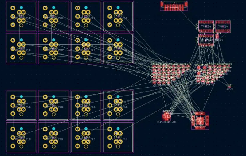
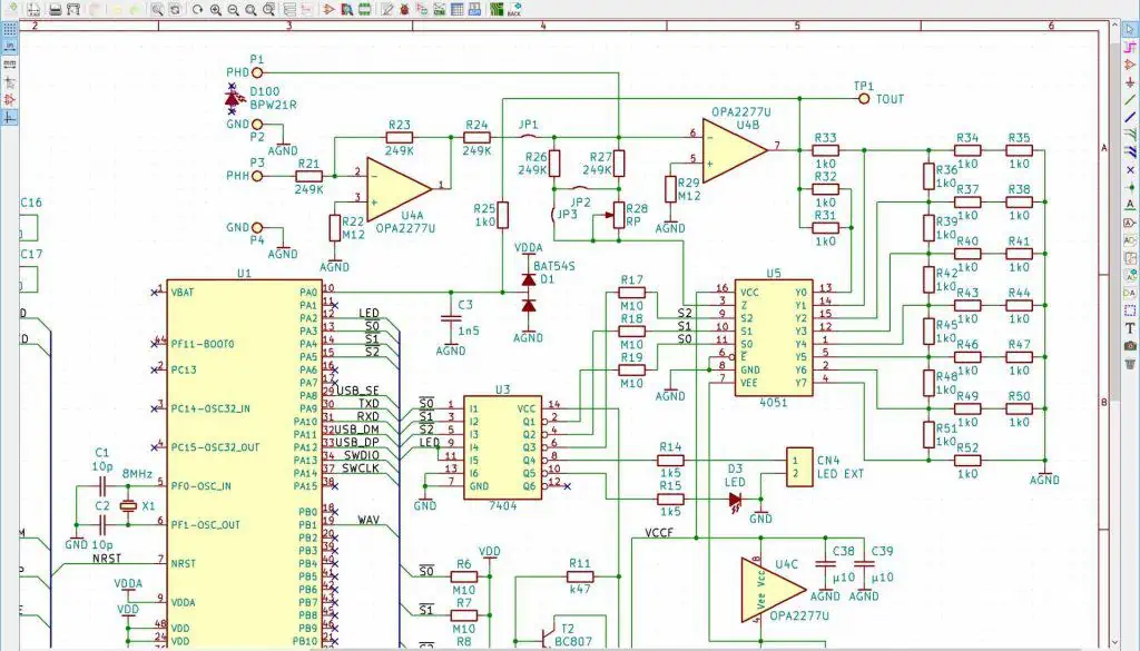
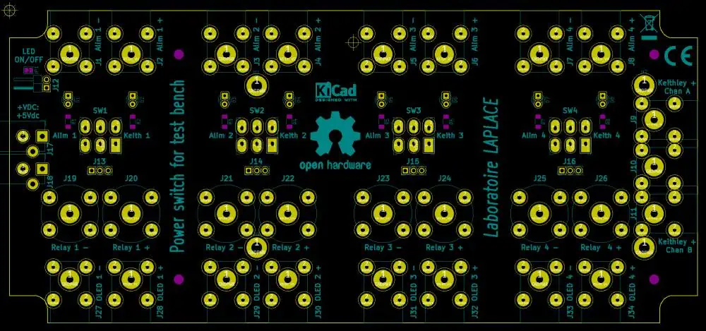
KiCad EDA suite is a powerful open-source electronics design automation platform enabling professionals and hobbyists alike to take electronic systems from concept to final routed PCB layout.
A major advantage of using KiCad over some commercial EDA tools is it allows including multiple PCB configurations within the same project design.
This is beneficial when dealing with complex designs requiring several inter-dependent circuit boards or versions to fully implement the target electronics hardware end-product.
This article provides a step-by-step walkthrough on how to correctly structure and manage multi-board KiCad projects, leveraging inheritance relationships to maximize design reuse. Screenshots demonstrate the key steps involved.
Follow along to learn how to efficiently architect complex multi-PCB solutions as one Master Project in KiCad.
Multi-Board Project Scenarios
Some typical use cases where designing several PCBs as part of consolidated project in KiCad makes sense:
- Main Board + Daughter Boards – Eg. CPU board + display board combinations with interconnection through high density connectors
- Board Sets – Devices involving panels/racks with duplicate PCBs plugged into backplane bus structure
- Versions/Derivatives – Spinning off variants like HW version 1.0, 1.1, 1.2 of base design
- Master/Slave System – One primary controller PCB with additional peripheral PCBs
In above cases, instead of managing each PCB layout completely independently in isolated KiCad projects, you can define linkage and inheritance relationships between boards early on during the design phase. This allows propagation of changes across dependent boards later avoiding painful rework.
Let’s see how step-by-step.
Configuring Multi-Board Project Structure

The first step is to configure the project structure to accommodate multiple boards belonging to same overall system design. This sets you up to achieve maximum re-use and consistency across individual PCBs due to centralized configuration inheritance reducing duplication or variation by error through project life cycle.
Start Fresh New Project
Launch KiCad and select File > New Project > New Project
Pick any folder location to host the Master Project. This will hold all the individual PCBs and common data.
Create “Project Level” Schematic Folder
Click Add Existing Folder to Current Project toolbar button showing green icon with “plus” symbol.
Browse to folder projectname just created and select subfolder path:
Copy code
projectname/-schematics
This establishes main /-schematics folder for holding any common schematic documents used across ALL boards like power or interface definitions.
Generate Each Board#X Schematic Sheet
Still under the Common Schematic Folder path in left tree view, now create respective schematic document for EACH planned PCB layout board.
Right click mouse, select Create New Schematic
Do this sequentially to initialize first sheet schematic file individually for however many boards intended in full project scope.
Eg. For 4 PCBs:
- board1.sch
- board2.sch
- board3.sch
- board4.sch
schematic sheets now created ready for circuit drawing later for each planned board.
Next Complete PCBnew Configurations
Repeat the same process now instead under the main project root to initialize corresponding .kicad_pcb layout file for each board schematic created already
Eg. For 4 PCBs:
- board1.kicad_pcb
- board2.kicad_pcb
- board3.kicad_pcb
- board4.kicad_pcb
These .kicad_pcb files inside root will become respective PCB layout containers related to each schematic sheet after netlist import.
This table summarizes the multi-board project folder structure and file types configured:
| Location | File Type | Description |
|---|---|---|
| /project/schematics | .sch | Common Schematic Sheets |
| /project/ | .kicad_pcb | Individual PCB Layout |
We now have framework ready to start actual PCB design work!
PCB Circuit Schematic Design Stage

With blank schematic sheets created ready per board, we can begin capturing actual circuits and connectivity. Standard workflow applies just like single board project.
It helps conceptually dividing schematics as:
- Common Circuits – Schematics logic used by multiple boards eg. power input filtering section
- Base Circuits – Baseline schematics sections reused by derivative boards via inheritance
- Unique Circuits – Schematics logic only applying to that specific board
This distinction helps manage change control between shared versus child schematic sheets when alterations occur later down the development timeline.
Follow standard schematic capture best practices as well creating logical schematic architecture for each PCB through combination of:
- Part symbols from installed component libraries
- Bus lines to reduce complexity
- Hierarchical structure using sub-sheets to simplify
- Net and wire labeling
- Design rule checks to validate integrity of connections
Cross Probe Between Schematics
Use the KiCad Cross-probing toolbar icon showing magnifying glass symbol to quickly navigate across sheets to trace wires connections between schematics as complexity builds up.
Output Schematic Netlists
Upon finishing respective board’s schematic sheets design work, next output netlist connectivity file. Repeat this process individually for each board’s schematics.
Steps:
- Open respective
.schschematic sheet Tools > Generate Netlist > PCBNew Netlist- Save netlist as eg.
board1.netfor each board - Repeat generating one netlist per board in project
Netlists act as bridge linking logical schematic connectivity to physical PCB layout.
PCB Layout Routing Stage

With connectivity netlists files now available board-wise, we can focus attention to converting schematics into routed PCB.
Again standard workflow applies – initialize board sizes, import netlist, assign footprints, run ERC, place components, route traces until completion for EACH board independently.
However, some additional considerations working on complex multi-board projects include:
Cross Probing Between Layouts
Use the same Cross-Probe toolbar button to quickly navigate between layouts by clicking pushpin marker to understand connectivity spanning across boards.
Inheritance Concept
Leverage inheritance relationships early instead of duplicating similar circuits or networks again. Eg. Common power supply section from one layout can propagate to other boards via cross-probing rather than redrawing.
Validate Across Boards
Before finalizing layouts, cross-validate that schemes used for connectors, mounting holes, silkscreen artworks are consistent across boards which will eventually interface during system assembly stage downstream.
Final Manufacturing Output Handoff
Upon completing all PCB layouts routing and checks, last step is generating manufacturing CAM outputs – Gerbers, NC Drills, Assembly drawings etc. – needed to fabricate the bare boards with a PCB supplier.
Again same process done earlier for single board projects applies here.
Some pointers when submitting manufacturing gerber data for quotation:
- Send separate zip folders per PCB for clarity even though single project
- Use consistent file naming conventions indicating parent project
- Include precise bare board fabrication and solder masking requirements
- Provide accurate target quantities needed for each board reflecting overall system build volumes
This completes end-to-end design process to realize complex electronics systems made up of multiple PCBs configurations managed efficiently as one Master Project in KiCad EDA tool.
FAQs
What is the best folder structure for multi-board KiCad project?
Below folder architecture allows clean separation between common and board-specific logical assets when dealing with multi-PCB project:
/-projectname
- /schematics (common schematic sheets)
- power.sch
- busdef.sch
- /board1
- board1_schematic.sch
- board1.kicad_pcb
- /board2
- board2_schematic.sch
- board2.kicad_pcb
So keep shared documents in parent level folders while individual PCB data under respective child folder.
How do I check differences between PCB layouts in multi-board project?
When iterating on designs with multiple boards, it helps cross-validate differences between board Layout versions.
KiCad provides built-in layout comparative functionality:
- Open first board layout
.kicad_pcb - Select menu
Tools > Compare PCB Layouts - Browse and select second
.kicad_pcblayout design - Adjust ignore thresholds if needed under various comparison criteria
This does smart diff analysis reporting differences between layouts helping synchronize changes across dependent boards.
Can I split complex schematic across multiple sheets for cleanliness?
Yes, when working with multi-page schematics for big designs, instead of cramping up all logic into giant single sheet canvas, apply divide and conquer approach:
- Break down by functional modules
- Use hierarchical sheets and ports
- Cross link between sheets using invisible nets
- Show external connectivity through block symbols
This reduces scrolling needs and aids readability helping focus on specific logic section when making edits instead of getting overwhelmed viewing entire schematic complexity on one page.
Cross-probing facilitates navigation while ERC checks validate connections consistency between fragmented schematic sheets. Page index table helps map document structure when interfacing design reviews. So fully utilize tools at disposal to creatively architect complex schematics refinement modularly across multiple sheets using KiCad’s versatile EDA environment capabilities.
I hope this gives a good starting point for electronics designers to efficiently structure KiCad projects involving multiple PCB layouts instead of struggling managing disconnected documents. Follow the principled approach touching on configuration, re-use via inheritance, cross-validation between boards and version control to yield productivity benefits when dealing with high complexity multi-board system solutions as one Master Project.
