What is the use of ESD tray?

Introduction to ESD Trays

ESD stands for “electrostatic discharge”. This refers to the sudden flow of electricity between two electrically charged objects.

In the electronics industry, ESD can be extremely damaging to sensitive components such as integrated circuits, semiconductors, and printed circuit boards. An discharge as small as 30V can brick delicate electronics.

ESD trays help protect electronics from such discharges during manufacturing, storage, and shipping. They are conductive trays that safely drain static charges away from contents.

This article provides an in-depth overview on ESD tray uses including:

  • Protecting components from electrical damage
  • Maintaining integrity of sensitive electronics
  • Enabling safe PCB assembly workflows
  • Standard testing and classification
  • Proper handling and precautions

Let’s explore the critical role ESD trays serve for mitigating electrical discharges.

The Hazard of ESD Damage

To understand functions of ESD trays, it’s important to first recognize hazards posed by electrostatic discharges:

Permanent invisible damage – While certain ESD events cause immediate product failures, even smaller discharges can incrementally degrade performance and longevity. This builds up โ€œlatent damageโ€ challenging to recognize.

Lower reliability – ESD weakens electronic components, leading to premature field failures under thermal/mechanical stresses.

Financial losses – Damaged goods must be scrapped or trigger warranty returns. For products already shipped, replacement is expensive. Either scenario hurts profit margins.

Table below summarizes losses across the supply chain:

StageFinancial Impact
Component ManufacturingDie/wafer losses
PCB AssemblyRejected PCB assemblies
Product ManufacturingFinished product failures
In FieldWarranty returns and replacements

Table 1: ESD causes financial losses across the electronics supply chain

So while ESD safety is often an afterthought, in aggregate such preventable damage introduces major costs. Trays help mitigate risk.

How ESD Trays Work

ESD trays protect contents through a conductive surface that safely channels electrical charges to ground. This prevents static building up then suddenly discharging through sensitive components.

Figure 1: ESD trays safely drain charges away components.

Various standards dictate acceptable resistances that allow sufficient charge drainage without impeding functionality. Common requirements:

  • Surface resistance: Under 10^9^ ohms
  • Volume resistance: 10^4^ to 10^6^ ohms
  • Grounding: Via wrist strap or conductive table mat

With proper use, ESD trays form a safe ecosystem protecting electronics from static discharges throughout handling and shipping.

Next let’s explore popular tray applications.

Common Uses of ESD Trays

Major uses of ESD trays fall into three main categories:

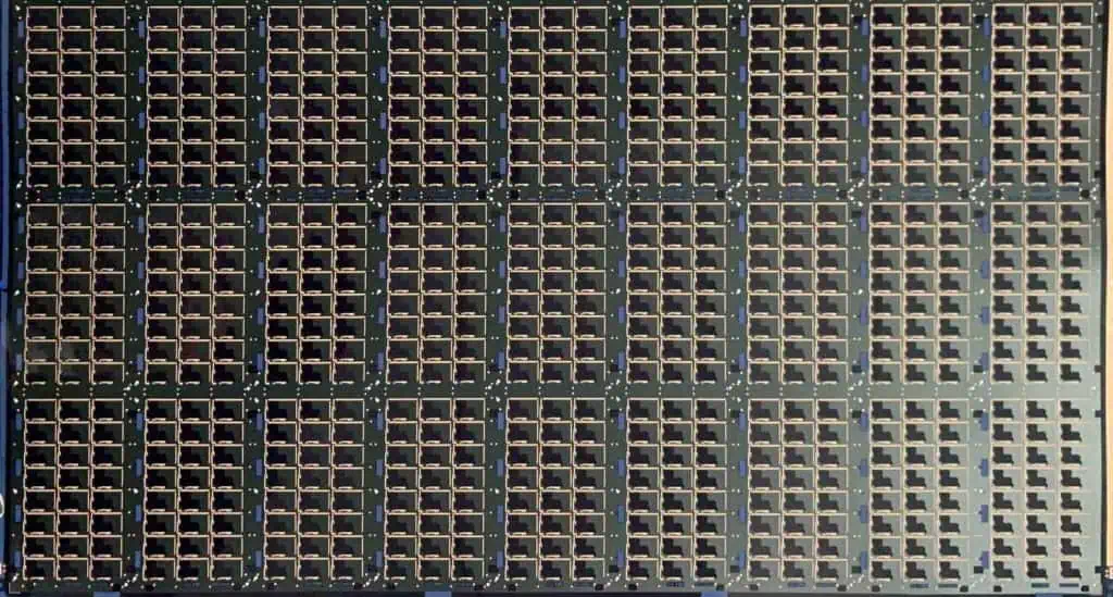
1. Protecting Sensitive Components

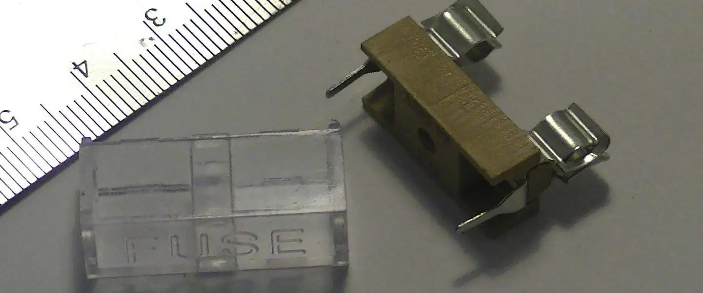
Vulnerable small items like integrated circuits, sensors and memory chips often ship in ESD trays or bags. Trays conveniently organize such tiny parts for storage or PCB population while safeguarding their integrity.

Figure 2: Trays protect vulnerable ICs, resistors, capacitors etc.

For prototyping, reusable trays avoid waste compared to single-use bags. They simplify organizing a spectrum of parts during development.

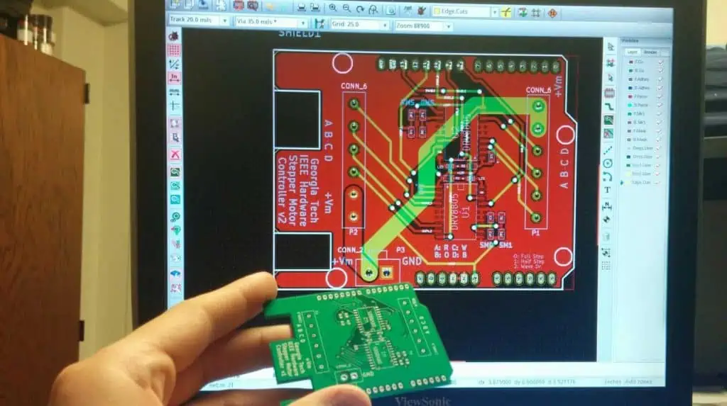
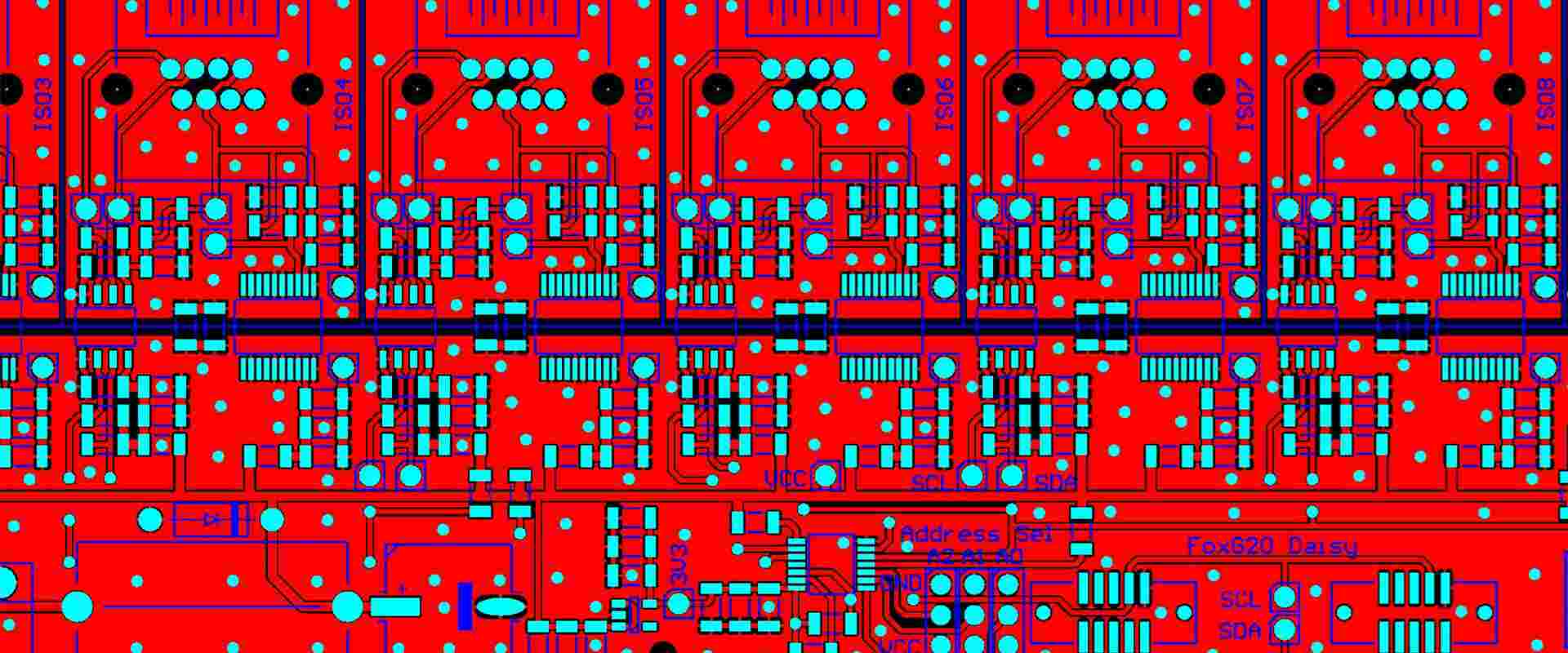
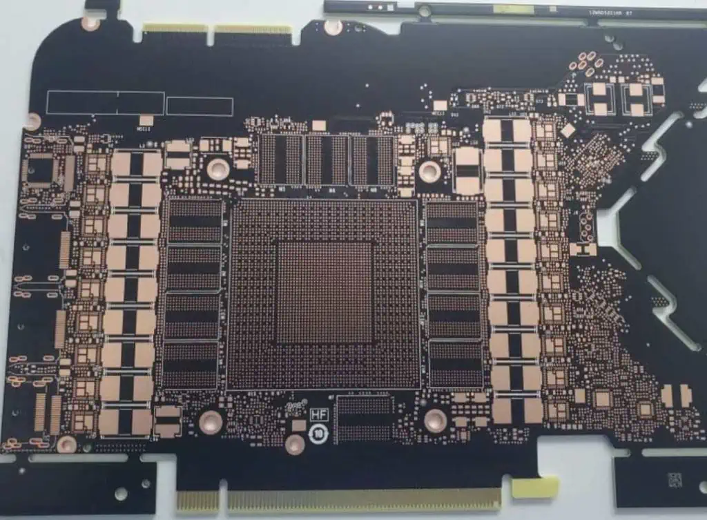
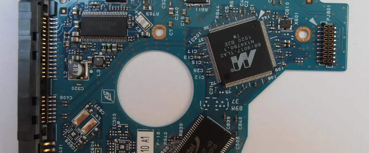
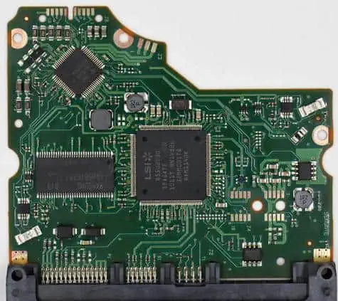
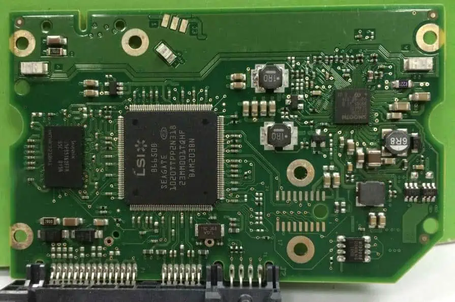
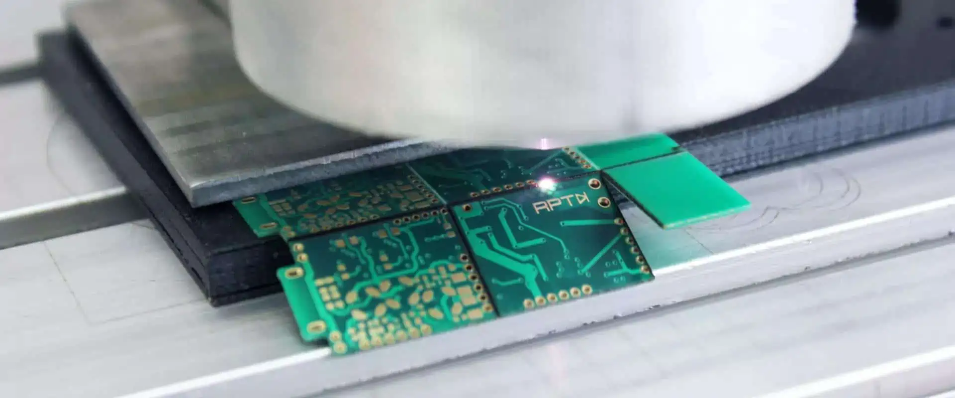
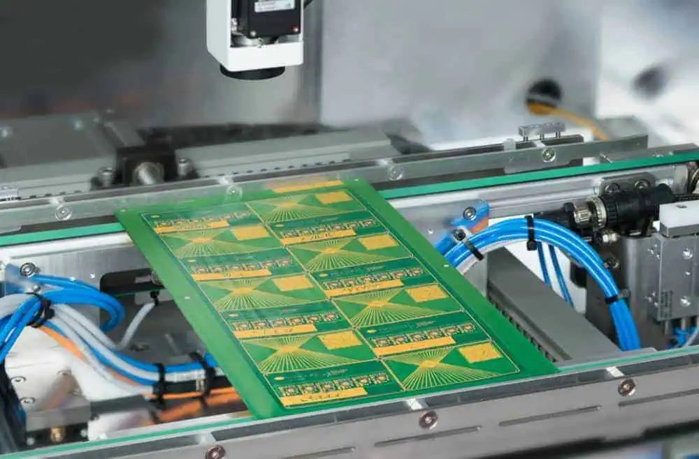
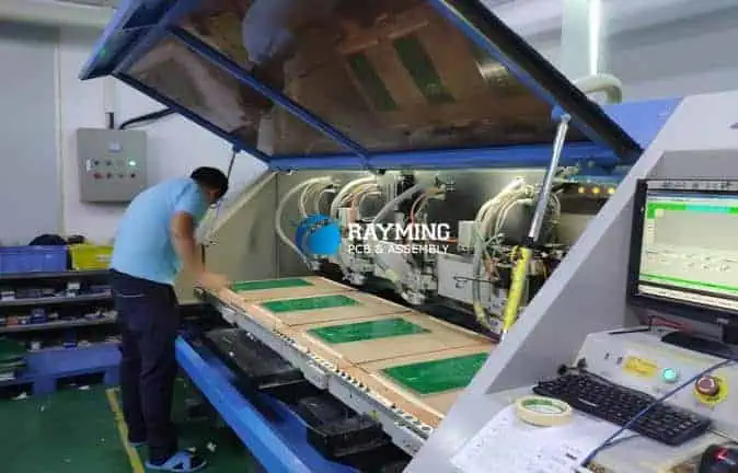
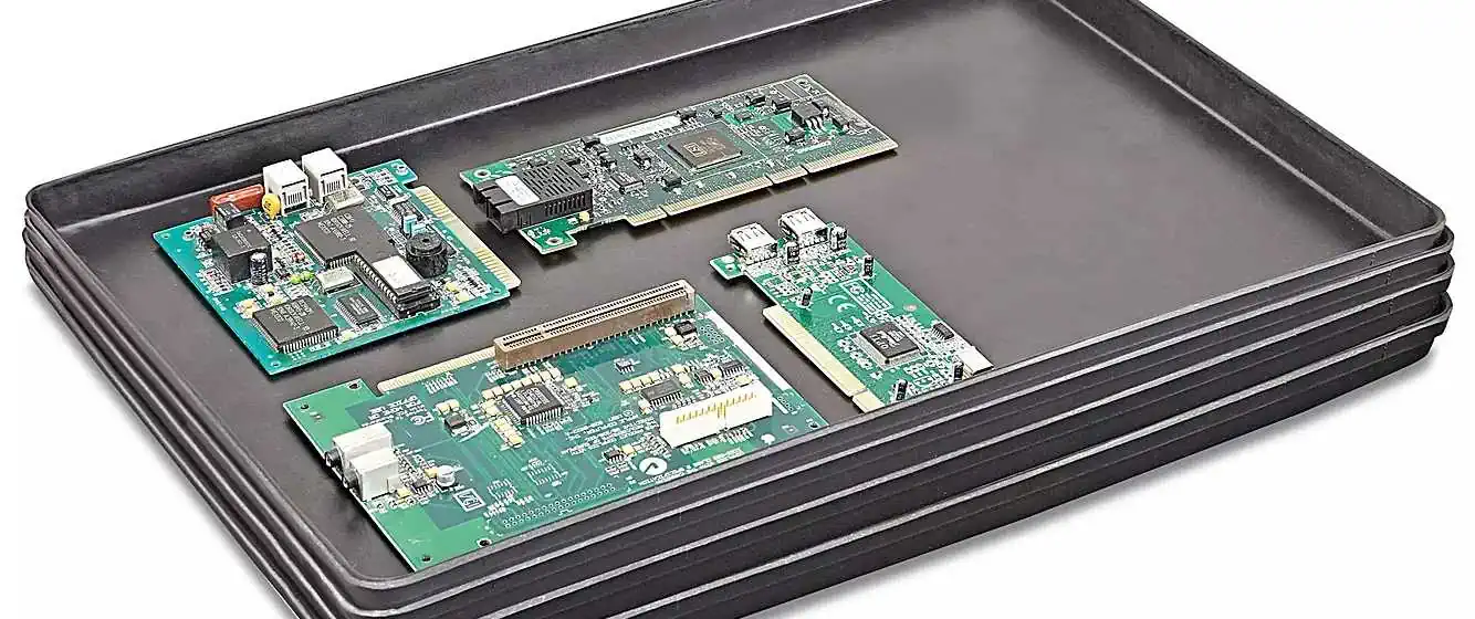
2. PCB Assembly Workflows

Entire populated or bare PCB assemblies are also commonly handled in ESD trays:

Figure 3: Trays enable safe handling through assembly.

This protects vulnerable boards through:

  • Transport between work centers
  • Storage between process steps
  • Protection from mechanical damage

Trays are mandatory when working with high frequency or exposed high density boards.

3. Shipping Protection

Finally, ESD trays are ubiquitous for packing electronics distribution:

Figure 4: Shipping protection with foam-lined trays

They enable safe transportation in two ways:

  1. Drain harmful static charges
  2. Shield components from physical impacts

Various foam liner materials facilitate snug component fit too.

In summary, ESD trays serve needs across electronics workflows – protecting during transportation, storage, and handling.

Next we’ll explore classifications and testing procedures.

ESD Tray Types, Testing and Standards

Not all ESD trays provide equal protection. Various testing procedures help classify trays based on capabilities to mitigate different ESD threats.

Major metrics include:

Surface resistance – Measures ease by which charges dissipate across tray surface. Too high allows static to accumulate.

Volume resistance – Evaluates conductivity through tray’s structural layer. Important for dissipating charges in embedded items.

Decay time – Assesses how quickly exterior surface neutralizes after charge removal.

Charge Shielding – Measures exterior fields with interior item statically charged.

Many industry and military standards now define adequate thresholds levels for tray compliance. Common ones include:

  • ANSI/ESD S20.20
  • IEC 61340-5-1
  • MIL-STD-1686

Below shows a typical classification system:

ESD Tray TypeSurface ResistanceVolume ResistanceDecay TimeShielding
Type 1<10E9 ohms<10E4 ohms<2 seconds>80%
Type 2<10E9 ohms>10E4 ohms<2 seconds>65%
Type 3>10E9 ohms>10E4 ohms>2 seconds<65%

Table 2: ESD Tray Classification per ANSI/ESD S20.20

So industry groups standardize tray testing to help engineers select appropriate protection levels. This enables matching risks posed by electronics with necessary mitigations.

Now let’s cover proper handling and precautions when using ESD trays.

Proper ESD Tray Use

While ESD trays provide a first line of defense for electronics, following best practices ensures their effectiveness:

  • Use wrist straps – Workers must wear grounded wrist straps to avoid accumulating charges.
  • Employ table mats – Conductive table mats drain charges from equipment like tools.
  • Ground trays – Ground points between trays and mats equalize potentials.
  • Avoid overloading trays – Overstuffed trays inhibit proper charge drainage.
  • Watch tray materials – Some plastics accumulate high static charges.
  • Control humidity – Low humidity enables static to build up.

Adhering to such mitigations is equally important as the trays themselves. Failing to ground personnel and their workstations creates safety gaps.

It’s also good practice to confirm tray condition periodically via resistance testing. Worn trays with degraded surface coatings lose their efficacy over time.

Let’s recap some key points.

Conclusion and Summary

  • ESD trays use conductive surfaces to safely channel electric charges away from sensitive electronics to protected ground points. This prevents static accumulating then suddenly discharging through components.
  • They serve critical needs protecting electronics across applications in component storage/shipping, PCB assembly workflows, and product distribution.
  • Industry standards dictate adequate resistances for charge dissipation without impeding functionality. Testing procedures classify trays accordingly.
  • Proper handling techniques including wrist straps, table mats and grounding are vital for trays to be effective. Failing to ground personnel undermines protections.

In essence, ESD trays form the backbone protecting electronics as they traverse global supply chains. Without mitigating such routine electrical threats, achieving acceptable yields and reliability would prove impossible.

Frequently Asked Questions

How do ESD trays work?

ESD trays use a conductive surface to safely channel electric charges away into ground points. This prevents static building up then discharging suddenly through sensitive electronics.

What electronics use ESD trays?

Integrated circuits, PCB assemblies, and finished electronic products all commonly rely on ESD trays while handling through assembly workflows or shipping distribution channels.

What causes ESD tray degradation?

Excessive use leading to surface scratches can degrade conductive coatings over time. Periodic resistance testing checks for worn trays needing replacement. Low production humidity also accelerates decline.

Are some plastics highly charging?

Yes, materials like polyethylene and PVC accumulate extremely high static levels and should be avoided for ESD tray construction unless using specialized additives.

How does humidity impact ESD trays?

Low humidity enables static to build up more easily. Maintaining production area humidity over 40% better facilitates charge dissipation across ESD trays into protect ground points.


What is the First Circuit Board in The World ? (History of PCB )

Before diving into the specifics of the first circuit board ever made, it’s helpful to understand the history leading up to their invention.

Circuit boards are the foundation of most modern electronics. They allow components like integrated circuits, resistors, capacitors, and more to be interconnected in a structured way. This enables signals to pass between components so complex circuits can be built.

But this wasn’t always the case. In the early days of electronics, all connections had to be made manually by soldering components together with wires. This was a slow, tedious, and error-prone process. It severely limited how complex circuits could become.

Printed circuit boards (PCBs) changed all of this by allowing components to be systematically arranged and pre-connected on a flat surface. This paved the way for electronics to become exponentially more advanced in the 20th century.

So who invented the first circuit board that made this revolution possible?

The Birth of the Circuit Board

The earliest predecessor of the circuit board was invented in 1903 by Albert Hanson, an employee at a German electrical engineering firm called AEG Telegraphy.

His creation consisted of thin strips of insulating tape onto which electrical wiring was pressed by a hot iron. While revolutionary for the time, it lacked many properties of modern PCBs.

The first true printed circuit board is widely credited to have been invented in 1925 by Austrian engineer Paul Eisler. Working in England at the time, he filed a patent for a method of printing electrical circuits onto an insulating baseplate.

His initial prototypes were made using a conductive ink printed onto bakelite sheets. Later he improved the process by using photolithographic etching similar to techniques still used today. This allowed much finer details than his original method.

So Paul Eisler’s circuit boards were the first that resembled modern PCBs as we know them. But they were still manufactured individually by hand.

The Transition to Mass Production

During World War II, the United States military began employing crude printed circuits in proximity fuzes for rockets to increase reliability.

This application demonstrated the usefulness of such technology for the first time on an industrial scale. It paved the way for the techniques developed by Eisler and others to be re-evaluated for mass production rather than one-off prototypes .

In 1947, the United States Army Signal Corps developed the first industrially mass-produced printed circuits at their laboratory at Fort Monmouth, New Jersey.

Engineers automated the photolithographic process developed earlier by Eisler so that sheets of circuits could be reliably reproduced without manual intervention. This transitioned printed circuits from a niche technology to one ready for widespread adoption.

The capabilities of circuits were still limited, however, by relying on individual discrete components soldered to the boards. Jack Kilby invented the integrated circuit in 1958, allowing entire circuits to be miniaturized onto single semiconductor chips. This led to another revolution in capability that married perfectly with printed circuit board technology.

So while Paul Eisler invented the first true circuit board, engineers at Fort Monmouth expanded on his work to enable mass production. And the capabilities of such boards were propelled forward tremendously by the later invention of the integrated circuit.

The First Circuit Boards

Now that we’ve covered a brief history leading up to their invention, what exactly did those first circuit boards made at Fort Monmouth in 1947 look like and what were they capable of?

They were quite primitive by today’s standards but revolutionary for the era. These were some key attributes:

  • Base Material: Paper-based phenolic resin
  • Maximum Dimensions: Approximately 3 x 5 inches
  • Copper Layer Thickness: 1 ounce (35 ฮผm)
  • Minimum Spacing Between Lines: ~100 ฮผm
  • One-sided with through-hole components
  • Reliably mass-producible via photolithography

The boards were initially one-sided with tracks on only one outer layer. Holes were drilled or punched into the board so component leads could pass through and be soldered on the opposite side. This “through-hole” design was necessary since surface-mount technology had not yet been invented.

While the capabilities of the initial circuit boards were modest, they led to rapid development once adopted widely. By the early 1950s, double-sided boards with plated through holes became common, greatly increasing circuit complexity.

And surface mount assembly eliminated the need for through-hole components, allowing further miniaturization. So while humble in origin, printed circuit boards enabled an electronics revolution once mass production methods were developed.

Early Single-Layer Circuit Board Capabilities

To visualize the humble beginnings of PCB technology, here are some key specs on those initial one-sided, paper-based boards first mass produced at Fort Monmouth in 1947:

Property Capability
Dimensions Up to 3 x 5 inches
Copper Thickness 1 ounce (35 ฮผm)
Minimum Spacing ~100 ฮผm
Layers 1 conductive layer
Maximum Components ~15-30 components
Component Types Through-hole parts
Materials Paper phenolic
Frequency <1 MHz

Table: Specifications of some of the earliest single-layer printed circuit boards.

While the first circuit boards were modest by today’s standards where boards with 12+ layers are common, they represented a tremendous leap forward in electronics manufacturing at the time. This paved the way for rapid advancements in capability in the coming decades.

Driving Adoption Through Military and Space Applications

Following their initial development at Fort Monmouth in 1947, printed circuit boards quickly gained adoption in American military applications during the 1950s.

Use of PCBs aligned nicely with military goals to miniaturize electronics as much as possible for applications including but not limited to:

  • Missile guidance systems
  • Airborne radar systems
  • Communication radios

Their ability to reliably interconnect miniaturized discrete components in a structured way facilitated this downsizing trend. And as integrated circuits emerged later around 1960, the advantages grew tremendously.

The American space program, which was largely driven by military-trained engineers, brought further demand for printed circuits. In particular, their reliability and resistance to vibration and mechanical stresses fit the needs of space flight.

Throughout the Cold War decades, PCB advancement ran hand-in-hand with military and space objectives, bankrolling continued progress. Commercial applications followed later once initially prohibitively high costs came down.

This military/aerospace lead nurtured PCBs through their infancy until economics expanded their reach more broadly in the 1960s and beyond.

The explosion of commercial PCB applications

By 1965, the manufacture of printed circuit boards in the USA exceeded $1 billion dollars (over $8 billion today). [11] No longer just a niche military product, they now served many commercial applications including:

  • Television sets
  • Radios
  • Business computers
  • Control systems
  • Test and measurement equipment

And demand further accelerated through the late 1970s as new applications arose including:

  • Personal computers
  • Video game consoles
  • Handheld calculators
  • Home appliances

As printed circuits facilitated automated assembly, manufacturing costs fell low enough for broad consumer product adoption. And multi-layer boards drove up interconnect capabilities to support increasingly complex circuitry.

So over just two decades following their invention, PCBs transitioned from narrow military applications to a backbone enabling the electronics industry as we know it today. And capabilities continues to grow according to Moore’s Law thanks to perpetual advancement.

Modern Circuit Boards

Printed circuit board technology has continued advancing rapidly since those initial single-sided versions first mass produced around 1950. Here is a comparison:

Property Early 1950s Today
Dimensions 3 x 5 inches 24 x 24 inches+
Layers 1-2 conductive layers 12+ conductive layers
Minimum Spacing ~100 ฮผm under 50 ฮผm
Materials Paper phenolic Ceramic, FR-4 fiberglass
Frequency <1 MHz Multi-GHz
Components 10s per board 1,000s per board

Table: Comparison between capabilities of early 1950s printed circuit boards vs. modern boards.

So in the 70+ years since their invention, PCB capabilities across factors like layer counts, component density, operating frequencies and more have increased by orders of magnitude. Driving this progress is a combination of:

  • Electronic design automation (EDA) software
  • Progress in manufacturing techniques
  • Advances in materials science
  • Higher purity materials
  • Economies of scale

And the electronics revolution enabled by printed circuits shows no sign of slowing down. So while humble in origin, the first circuit boards seeded technology that continues rapidly evolving today.

Frequently Asked Questions

Who invented the first printed circuit board?

The first true printed circuit board resembling modern technology is widely credited to have been invented in 1925 by Austrian engineer Paul Eisler. He filed a patent for a method of printing electrical circuits onto an insulating baseplate using conductive inks and photolithography.

How were early printed circuits mass produced?

Building on Paul Eisler’s work, engineers at Fort Monmouth, New Jersey developed the first photolithographic processes suitable for industrial mass production of printed circuits in 1947. This transitioned them from a niche technology to one ready for widespread adoption.

What materials were early PCBs made from?

Initially paper-based phenolic resin laminates which provided adequate insulation and mechanical stability but were limited in performance compared to later fiberglass-based materials. In the 1950s, FR-4 fiberglass quickly emerged as an improved base material.

How did early PCB capabilities compare to today’s?

Extremely primitive! Those first mass produced boards around 1950 were one-sided with simple through-hole components and dimensions under 5 inches. Today we have enormous boards with 12+ copper layers capable of holding thousands of tiny surface mount components.

How did early adoption of PCBs align with military objectives?

The American military drove early PCB development starting in WWII to achieve electronics miniaturization, reliability and vibration resistance needed for missile guidance and other applications. This nurtured advancement through the critical early stages until costs fell sufficiently for broader commercial adoption.

And that covers some key points on early printed circuit board history – from their origins in Paul Eisler’s 1925 patent to how the technology became revolutionized by mass production methods a few decades later. Let me know if you have any other questions!


How do you Remove Flux Residue From PCB?

Flux agents are essential chemicals applied during soldering to facilitate strong metallurgical bonding between component leads and copper PCB pads. However, leftover flux residues can cause issues like electrical leakage, dendrites, corrosion or failures under humidity if not properly cleaned post-soldering.

This article provides a comprehensive guide to managing flux residues including:

  • The flux cleaning imperative
  • Water and solvent-based cleaning approaches
  • Process considerations and challenges
  • Cleanliness validation methods
  • FAQs related to post-solder flux removal

Learning flux residue removal best practices helps improve electronics assembly yields, reliability and long term functionality.

The Critical Need to Remove Flux

While flux residues seem innocuous, they can severely impact PCB performance and lifespan if left on assemblies after soldering.

Some potential reliability risks posed by ionic flux residues like weak organic acids or halides include:

Electrical leakage – Absorbs moisture and creates current leakage paths

Corrosion – Gradually corrodes copper traces or component leads

Dendrites – Grows conductive metallic crystals eventually causing shorts

Insulation resistance degradation – Allows resistive power losses through surface films

Cosmetic issues – Causes surface discoloration or tacky coatings

So removing flux after soldering is an indispensable process step to ensure lasting PCB integrity.

Next letโ€™s contrast cleaning approaches using solvents versus aqueous methods.

YouTube video

Solvent Cleaning Agents Used

Solvent cleaning refers to using organic chemical solutions to dissolve then rinse away flux residues. Some typcal solvents include:

Isopropyl alcohol (IPA) โ€“ Rapidly evaporates with wide materials compatibility

Acetone โ€“ Stronger solvency but more aggressive requiring dilution

Terpenes โ€“ Plant derived citrus cleaners with reduced environmental impact

Solvent cleaning can be performed by manual wiping, immersion tanks, inline conveyors and ultrasonic or pressure spray systems with vacuum drying.

Some benefits of solvent cleaning include:

  • Removes diverse flux chemistries like rosin mildly, no-clean, water soluble types
  • Penetrates tight gaps under components to access hidden residues
  • Quickly dissolves both ionic and non-ionic contamination
  • Enables isolated spot cleaning of small areas when needed
  • Wide availability of chemical compatibility data to guide material selections

However, solvents also pose flammability, waste disposal and regulatory emission control challenges. This motivates aqueous process alternatives.

Aqueous Flux Residue Cleaning Processes

Water-based cleaning relies on ionized water’s natural solvency power combined with detergents at elevated temperatures and impingement pressures to reliably remove residues.

Some common aqueous cleaning systems include:

Immersion washers โ€“ Features multiple staged baths for gross soil removal down to rinses

Inline washers โ€“ Continuous conveyors passing boards through spray detergent zones + rinses

Ultrasonic systems โ€“ Energized baths generating focused cavitation shockwaves hitting board surfaces

Pressure spray washers โ€“ Direct high impingement jets + mechanical scrubbing on boards

Condensation washers โ€“ Controlled condensing humidity enclosures to lift residues

Water cleaning is attractive because it avoids hazardous chemical disposal requirements and utilizes lower cost aqueous detergents. Thermal energy efficiently substitutes harsh solvents.

Key benefits of aqueous cleaning encompass:

  • Eco/worker friendly with simpler waste water treatment
  • Readily accessible and plentiful water media
  • Heated spray and ultrasonics provide excellent cleaning power
  • Programmable automation adaptable for high volume applications
  • Reliable reproducibility following validated cycles

On the downside, aqueous processes lack penetration into tight spaces. Water sensitivity limits components exposure allowances too. Despite such constraints, appropriate water-based cleaning systems prove highly effective for suitable PCB assembly applications when engineered properly.

Now that we distinguished solvent versus water-based options, letโ€™s elaborate best practice process considerations to deploy either approach effectively.

Optimizing Process Parameters for Flux Removal Efficiency

Successfully removing flux residues depends greatly on selecting optimal equipment settings and following disciplined operating protocols tailored to your boards.

Here are some key process parameters to optimize:

Cleaning Media โ€“ Match solvent or water-based detergent chemistry to flux type and processing goals. Start with manufacturers recommended formulations.

Concentration โ€“ For aqueous cleaners, calibrate detergent % dilution carefully for target soils. Excessive concentrations waste chemicals whereas low concentrations risk cleaning shortfalls.

Exposure Time โ€“ Ensure adequate dwell time for cleaning agents to penetrate, solubilize and detach all residues present. Complex boards need longer durations.

Temperature โ€“ Heated media between 50-80ยฐC boosts cleaning dynamics substantially compared to room temperatures for dried residues. But donโ€™t overheat beyond chemical or component limits.

Flow Rate (solvent) โ€“ Adjust solvent spray flow to flood boards without excessive impingement pressure causing component blow-off defects.

Impingement Pressure (aqueous) โ€“ Steam and spray jets help blast off hardened residues mechanically when delicately optimized in psi/bar units without deforming boards.

Frequency – Replenish baths regularly based on accumulated soil loading quantified in microSiemens to maintain cleaning efficiency as contaminants saturate solutions.

Careful process testing starting from baseline presets then gradually adjusting within equipment safe ranges determines optimums empirically case-by-case based on cleaner qualifications.

Next weโ€™ll highlight some practical challenges working with either cleaning technique.

Comparison of Solvent vs Aqueous Challenges

While both solvent and water cleaning methods scrub residues when done properly, each encounters characteristic implementation difficulties in applications:

Solvent Cleaning Challenges

  • Flammability risks requiring costly special equipment and safety procedures
  • Hazardous waste disposal, emissions regulations and records compliance
  • Component or housing damage from aggressive solvents like acetone
  • Manual cleaning consistency challenges at high production volumes
  • Residue re-deposition drying stains if not handled properly

Aqueous Cleaning Challenges

  • Prolonged water exposure degrades moisture sensitive components
  • Reaches under tight component gap limitations
  • Mixed material compatibility constraints like magnesium or glass restrictions
  • Tank maintenance and microbiological contaminant risks
  • Stains or white water marks if inadequately rinsed and dried

Accounting for these unique constraints guides appropriate water or solvent-based flux residue cleaning selection for targeted assembly needs.

Finally, validating cleaning effectiveness proves highly beneficial.

Techniques to Verify Adequate Flux Residue Removal

While visual inspection checks for noticeable surface residue left on PCBs post-cleaning, several quantitative techniques reliably validate cleaning performance:

Ion Chromatography Analysis โ€“ Detects microscopic inorganic anion/cation content extracted from cleaned boards correlating well with residual ionic contamination. Parts per million sensitivity ensures boards are chemically clean.

Combustion Infrared Detection โ€“ Burns-off traces organics present then analyzes retained carbon content accurately determining any organic residues down to low PPm levels.

Oddy Test โ€“ Exposes cleaned coupons to active and blank copper strips in humidity and heat to check for dendrite growth assessing residue corrosivity tendency.

Surface Insulation Resistance – Measures electrical resistance across comb pattern test cards before and after cleaning, looking for order of magnitude reductions indicating surface contamination removal.

SEM Inspection โ€“ Scans high magnification SEM imaging across board surfaces confirming the complete absences of flux film or residues within equipment detection limits.

While adding test time and costs upfront, validating flux removal quality provides confidence regarding long term reliability over product lifespan for critical applications.

With key flux cleaning concepts covered, weโ€™ll wrap up by addressing common FAQs on the topic.

Frequently Asked Flux Residue Cleaning Questions

How do you know a PCB needs cleaning after hand soldering?

Visually inspect boards after hand soldering using bright side lighting at an angle to reveal residue films. Target hard to reach areas underneath component overhangs using an angled mirror. If hazy residue shows and especially if it feels tacky when touched, cleaning proves necessary to avoid electrical or corrosion issues long term.

What PCB cleaning methods work for large production volumes cost effectively?

For production environments producing hundreds or more boards daily needing cleaning, engineered inline aqueous cleaning systems provide the most cost effective, reproducible and automated process capabilities. These machines reliably meet high output needs while minimizing labor compared to batch processes.

How do ultrasonic and spray washers compare for removing baked-on flux?

While ultrasonic cavitation helps lift some thick flux layers, directly aiming high pressure or temperature sprays >80ยฐC at the afflicted areas for extended intervals works best for stubborn baked residues. Precision wand attachments target cleaning streams. The combined chemical and mechanical attack focus breaks down the hardened layers efficiently.

Why does water temperature matter so much when cleaning flux residues?

Heating water to 50-60ยฐC significantly accelerates flux dissolution kinetics following Arrhenius rate equations regarding reaction speeds exponentially improving with temperature. So rather than solely relying on detergent chemistry, harnessing thermal activation proves highly beneficial by preventing temperature limitations slowing cleaning.

How do you apply solvents for cleaning limited area touch-ups?

For isolated rework spots needing touch-up cleaning, precision cleaning pens flooding just the desired area with pressurized sprays of solvent work well. IPA, acetone and terpene pens confinement localizes application preventing widespread residues. Manual wiping then absorbs dissolved flux away.

Conclusion

In summary, allowing flux residues to remain on populated PCBs poses major reliability risks from electrical leaks, corrosion, dendrites and insulative surface films during operation. Assemblies therefore require proper validation of residue removal after soldering using metrics like ionic contamination, SIR comb testing or microscopy inspection.

Solvent and aqueous cleaning agents prove highly effective for dissolving and detaching flux films when judiciously matched to process needs based on considerations like media temperature, concentration, exposure interval and impingement pressure optimization. Accounting for flammability hazards, waste handling, material compatibility and drying defects guides proper implementation.

By mastering PCB flux residue removal techniques, engineers safeguard electronics functionality and longevity over targeted product lifetimes in the field. This best practice empowers quality outcomes and avoids premature operational failures related to post-soldering residues.

What is Fr4 ultra-thin PCB ?

Printed circuit boards (PCBs) form the foundation of electronics, providing the platform to mount and interconnect components using copper traces on an insulating substrate. PCB technology has evolved tremendously over decades, with modern requirements demanding thinner, smaller, higher density, more flexible and lower cost designs.

Ultra-thin PCBs specifically feature extremely slim board thicknesses below 1.6 mm (0.063 inches) down to as thin as 0.15mm (0.006 inches). This article provides a deep dive into ultra-thin PCB advancements – answering what they are, why thickness matters, manufacturing techniques, key applications, challenges and outlook for the future.

What is FR4 Material?

To understand ultra-thin PCBs, we must first grasp the basics of the FR4 glass reinforced epoxy laminate material that makes up circuit boards.

FR4 is the most common PCB substrate material, composed of woven fiberglass cloth reinforcement embedded within an epoxy resin binder. The epoxy resin system imparts mechanical rigidity while the glass fibers provide strength to the board.

Some key properties of FR4 material include:

  • Good electrical insulation with high resistivity
  • Flame retardancy for safety
  • Moderate flexibility & bending before cracking
  • Capability to withstand PCB assembly processing temperatures
  • Relatively low cost

One shortcoming of standard 1.6 mm thick FR4 boards is that they lack flexibility to adapt to compact device designs and emerging needs.

This sparked motivation to create ultra-thin variants of the trusted FR4 material system with thinner dielectric substrates. Let’s analyze some of the benefits driving ultra-thin PCB adoption next.

Why are Ultra-Thin PCBs Needed?

Some of the top reasons ultra-thin PCB development is essential include:

Weight Reduction

Consumer devices like phones, laptops, tablets, IoT products and wearables demand thinner and lighter electronics to improve portability and ease of use. Shaving down PCB weight via ultra-thin boards aligns with this priority.

Even marginal PCB weight reductions multiply into substantial savings from the perspective of a major electronics OEM producing millions of units per year. This spurs tech innovation into thinning approaches.

Increased Flexibility & Conformability

Many modern gadgets feature non-flat, contoured housings needing flexible PCBs able to conform around molded enclosures or fold into small volumes. Ultra-thin boards provide enhanced flexibility to adapt within restricted 3D spaces inside products.

Tighter Packing of Components

Thinner boards allow components to be more densely packed together. This directly translates to smaller overall electronics hardware sizes, critically important in compact hand held tools, IoT devices, aerospace and defense systems.

Improved Thermal Performance

Thin boards offer lower thermal resistance to efficiently dissipate heat from hot components mounted directly on them. Less substrate thickness means heat pipes and sinks contact closer to actual chips, keeping junction temperatures cooler.

Lower Dielectric Losses

Ultra-thin laminates minimize signal losses across the board substrate dielectric medium. This allows high speed communication signals relying on tightly controlled impedance environments to travel faster and further across PCBs.

Next we’ll analyze popular processes to reliably manufacture these ultra-thin circuit boards.

Key Manufacturing Techniques for Ultra-Thin PCBs

Bringing reliable ultra-thin PCBs into high volume production has required material science innovations paired with advanced fabrication processes.

Here are 5 pivotal manufacturing technologies enabling ultra-thin PCB production at scale:

1. Prepeg Materials Innovation

At the heart of ultra-thin PCB mass production is the development of thin prepreg bonding films. Prepreg refers to the thermoset epoxy resin system reinforced with fiberglass cloth.

Cutting edge processes can reliably cure ultra-thin prepreg materials down to 25-50ฮผm thickness with tight uniformity across large panel sizes. This forms the foundation for thin boards.

2. Sequential Lamination

During lamination, prepreg sheets are stacked up symmetrically along with inner layer circuitized cores within a mechanical press. Heat and pressure bonds adjacent layers into an integrated board.

However standard lamination pressures crack thin materials. So sequential lamination applies lighter pressures through multiple inflection points to bond thin cores without damaging them.

3. Advanced Drilling Techniques

Ultra-thin laminates require especially tight precision drilling to create interconnect vias between layers with strict positional accuracy tolerances below 5ฮผm deviation. Quality issues become magnified at thinner dimensions.

Specialized drilling methods like lasers, plasma and UV photo-via help form high density microvias within ultra-thin boards too fragile for traditional mechanical drilling.

4. Modified Surface Finishes

Standard PCB surface finishes like HASL lead are too thick for proportionally coating ultra-thin boards which distorts dimensions. So ultra-thin PCBs leverage low profile ENIG, ENEPIG or OSP finishes to protect traces without oozing over fine features.

5. Special Handling Requirements

Thin boards under 0.4mm thick are extremely fragile, needing custom racking solutions to transport panels across fabrication lines. Vacuum assisted tooling gently handles the fragile boards during processes like drilling, routing and optical inspection.

This covers approaches enabling reliable manufacturing of ultra-thin FR4 circuit boards. Next we’ll highlight some key end use applications taking advantage of ultra-thin board properties.

What Industries Use Ultra-Thin PCBs?

Some leading applications benefitting from ultra-thin PCB technology spans industries like:

Consumer Electronics

  • Smartphones, tablets & wearables
  • Laptops, game consoles
  • Drones, IoT gadgets

Computing

  • Servers, data storage drives
  • Mini/micro computing

Automotive

  • In-vehicle infotainment
  • Drive data recorders
  • Vehicle tracking GPS

Aerospace/Defense

  • Avionics equipment
  • Missile guidance
  • Military radio hardware

Medical

  • Implants, hearing aids
  • Diagnostic imaging

Common themes across these market segments include needs for weight reduction, tightly constrained PCB sizes, curve shaped enclosures, enhanced high speed signals or rugged durability.

Let’s highlight two specific product examples leveraging ultra-thin boards:

Wearable Health Trackers

Health monitoring wrist bands and smart watches rely on thin, flexible PCBs to wrap around contours comfortably while packing electronics tightly. Ultra-thin builds allow more PCB layers routing signals from sensor ICs across small volumes.

Servers/Data Centers

Servers demand optimal cooling and signal integrity for processing reliability. Ultra-thin high layer count boards place chips closer together with lower thermal resistance paths to heat sinks. Dielectric losses are also minimized for high speed signals across backplanes linking server blades.

These demonstrate applicability of thin PCBs towards current technology innovations. Next we’ll highlight some handling precautions when working with thin laminates.

Practical Challenges Associated with Ultra-Thin PCBs

0.2mm thin pcb board

While delivering valuable advantages, ultra-thin PCB technology also poses some unique challenges requiring special care during fabrication, assembly and testing.

Some common challenges when dealing with thin boards include:

Fragility and Susceptibility to Damage

Laminates below 0.8mm thickness become extremely fragile and prone to cracking, flexural damage, bow and warp defects both during manufacturing processes as well as shipping or handling stress.

Reduced Thermal Mass Deforms Easily

The low thermal capacity of thin laminates makes them quickly deform under heat exposure. Temperatures above Tg (glass transition) cause temporary or permanent misshaping if not specially clamped during soldering reflow.

Prone to Twist, Skew and Registration Errors

Insufficient handling rigidity through various fabrication processes causes stacking registration issues leading to skew or misaligned interconnect vias between layers.

Produces Insufficient Peel Strength

If prepreg resin flow does not properly bond inner layer interfaces enough, interlaminar separation or fractures result destroying board integrity and reliability.

Challenging Rework and Modifications

Required drilling, routing or pad repairs post-production pose risks of fracturing ultra-thin boards which lack reserves to withstand modifications.

By understanding these limitations unique to thin boards, engineers can account for them by specifying appropriate handling fixtures, qualification testing, design rules and assembly clamping.

Now that we reviewed background, benefits, manufacturing and challenges, we’ll conclude by projecting the future potential for ultra-thin PCBs.

The Outlook for Ultra-Thin Board Development

Ultra-thin PCB technology has come a long way enabling innovative electronics across industries like consumer, medical, defense and automotive โ€“ but additional advances are still needed moving forward.

Continued Thinning

There are few signs of the drive towards thinner, lighter electronics abating given continue market demands. This pressures board shops to develop processes reliably achieving mainstream laminate production below 0.2 – 0.3mm thickness. Materials resiliency and microvia reliability become heightened concerns needing focus with ongoing PCB thinning extremes.

Hybrid Flex-Rigid Designs

Rather than purely rigid ultra-thin boards, many applications call for combination constructions which integrate even thinner flexible PCB materials into specific bendable zones. More research into robustly bonding thin flex-rigid hybrid designs promises better electronics adaptations to complex 3D shapes.

Improved High Density Integration

Thinner laminate stacking allows more densely integrated components, but sufficient heat dissipation becomes critical. Thermal vias, embedded channels and exotic fillers manage heat buildup while enhancing packing densities through vertical interconnect approaches like buried resistor/capacitors and staggered through mold vias.

Cost Pressures

Ultra-thin fabrication processes remain specialized relative to standard PCB production which risks slowing mainstream adoption. However as material volumes scale up and equipment makers tailor solutions towards thin boards, size and cost pressures should ease in the long term.

In summary, ultra-thin PCB technology helps enable transformative lighter and smaller next-gen electronics. Ongoing materials science and manufacturing process breakthroughs promise to spread ultra-thin board capabilities towards exciting new applications in the future.

Frequently Asked Questions

Can conventional FR4 resin be thinned arbitrarily without quality issues?

No, common FR4 material properties like glass transition temperatures, coefficient of thermal expansion, modulus of elasticity, tear strength and moisture absorption behave quite differently with excessive thinning below 0.3mm. Without re-formulating resin chemistry or additive adjustments, excessive thinning hurts PCB reliability.

What are typical thin board defect rates relative to standard 1.6mm PCBs?

Defect rates typically rise considerably for PCBs under 0.8mm thickness, often over 10X higher vs standard boards. Process defects occurring during lamination, drilling,routing, plating and handling damage are especially prevalent requiring extra inspection vigilance.

What design strategies help compensate ultra-thin PCB fragility?

To safeguard thin PCB integrity, designers avoid cutouts or notches reducing strength, specify wider conductor/spacing rules as process tolerance buffers, use adhesive stiffening bars/frames, eliminate flexible zones from boards, and analyze vibration/shock loads for worst case resonances.

Can multiple ultra-thin cores be interleaved to form thicker boards?

Yes, multiple ultra-thin cores around 0.2mm thickness can be stacked together with adhesive sheets in between to fabricate multi-layer boards exceeding 1.6mm total thickness. This helps circumvent thinner core handling issues, while reducing critical signal layer dielectric constant relative to thicker cores.

What are typical price premiums charged for ultra-thin PCB prototyping?

Because of specialized materials and customized racking fixtures needed for gentle handling, expect prototyping costs between $1500-2500 for small batches of 5-10 boards on average โ€“ likely over 10X the expense of standard prototypes board. Cost reduces substantially for higher volume production over 500-1000 units as dedicated tooling gets reused.

Conclusion

To conclude, ultra-thin PCB technology enables lighter, smaller and more integrated electronics desired across industries – but poses unique manufacturability challenges still being resolved to reach mainstream adoption. Striking the optimal tradeoffs between thinness, cost and reliability remains an evolving art mastered gradually through accumulated PCB materials & process knowledge paired with design ingenuity.

What does a Fuse Holder do in a PCB circuit?

A fuse holder is a small device designed to hold a fuse and connect it safely to a printed circuit board (PCB). Fuses are important safety components in electrical circuits as they protect the circuit and connected components from overcurrent.

The key things to know about fuse holders in PCB circuits are:

Terminology

  • Fuse: A safety component designed to blow or open when excessive current flows in order to protect the circuit
  • Fuse holder: A device to physically hold and electrically connect a fuse to a PCB
  • Overcurrent: When more current flows than what the circuit is designed for
  • Short circuit: An unintended low-resistance path in the circuit

What They Do

  • Provide safe and secure mounting for fuses on PCBs
  • Allow faulty fuses to be easily identified and replaced
  • Protect PCB components like integrated circuits (ICs) from damage due to overcurrent

How They Work

  • Fuse holder has metal contacts to electrically connect the fuse in series with the PCB circuit trace
  • When overcurrent happens, fuse blows/opens and interrupts excessive current
  • Prevents short circuit current from continuing to flow in the PCB

Types

  • Through-hole fuse holders
  • Surface mount fuse holders
  • Chassis-mount fuse holders
  • Fuse clips

In the rest of this 5000+ word guide, we’ll explore fuse holders for PCBs in further detail – covering terminology, functions, selection factors and installation best practices with the help of tables and images.

What is the Role of a Fuse Holder?

Protects Circuit Functionality

The primary role of a fuse holder in a PCB circuit is to provide a safe and reliable connection point for a fuse to protect the overall functionality of the circuit.

When overcurrent occurs and too much current flows, the fuse sacrifices itself by blowing and opening the circuit. This interrupts the excessive current, preventing further damage to valuable components downstream on the PCB.

So in short, the fuse holder allows the fuse to do its critical protection job.

Facilitates Fuse Mounting and Replacement

In addition to enabling fuse protection, another key role of a fuse holder is to provide a standardized and safe means to mount fuses onto a PCB. This makes fuse blowing visually identifiable and allows blown fuses to be conveniently accessed and replaced by an operator.

Without a proper holder, fuses would need to be manually soldered onto PCBs, making replacement tedious and unsafe. Fuse holders therefore improve safety, make fusing more modular and allow PCB assemblies to be serviced and reused.

Provides Secure Electrical Contact

Fuse holder contacts firmly grip the fuse blades or end caps to form a stable electrical connection between the fuse and PCB copper traces. This helps avoid issues like high resistance or intermittent contacts across the fuse which can impair circuit functionality. Proper finger pressure ensures the fuse remains seated securely inside the fuse holder.

So in summary, fuse holders play an indispensable role in harnessing the power of fuses to protect PCB functionality, while also enabling modular fuse mounting and reliable connectivity.

Key Functions

The four main functions of a fuse holder are:

  1. Protection – Allows fuse to safely break overcurrent
  2. Mounting – Holds fuse mechanically onto PCB
  3. Replaceability – Easy fuse access for maintenance
  4. Contact – Provides low resistance electrical connection

Types of Fuse Holders Used on PCBs

There are several common types of fuse holders designed to mount fuses onto printed circuit boards, each with their own sets of pros and cons.

The main types are:

1. Through-Hole Fuse Holders

Through-hole fuse holders are the most popular type of PCB fuse holder for prototyping and low volume production:

Features:

  • Two leaded pins for through-hole PCB mounting
  • Horizontal or vertical mount options
  • Wide fuse size compatibility
  • Very easy to manually install/replace fuses
  • Low cost

Applications:

  • General circuit protection
  • Common in electronics prototyping and testing

2. Surface Mount Fuse Holders

Surface mount fuse holders directly mount onto surface mount pads on a PCB:

Features:

  • Compact design with low height above PCB
  • Available for common fuse sizes like 1206
  • Fast automated SMT assembly compatible
  • Very stable with good resistance to shocks/vibration
  • Often have solder tabs under body for added strength

Applications:

3. Chassis Mount Fuse Holders

Chassis mount fuse holders feature threaded bodies which screw into a cutout hole on device chassis or enclosures:

Fuse Holder StyleImageDescription
Open chassis mountExposed fuse clips allow fuse accessibility from outside the chassis
Closed chassis mountShrouded clip design for applications needing IP rating or safety from live fuse clips

Features:

  • Robust screw mounted mechanical package
  • Compatible with wide range of chassis materials and thicknesses
  • Easy to replace fuses from outside device
  • Protects from accidental user contact with live fuse
  • Special versions meet IP67 rating for water proofing

Applications:

  • Industrial control boxes and power devices

4. Fuse Clips

Fuse clips provide a spring clamping receptacle to securely grip cartridge type fuses:

Features

  • Tight retention force avoids vibration issues
  • Wide compatibility with tube and cartridge fuses
  • Excellent high current capacity
  • Chassis or PCB mountable

Applications:

  • Heavy duty power electronics
  • Automotive, HVAC and Energy

This covers some of the most popular fuse holder types used with PCBs. There are also more application specific designs like waterproof power fuse holders found in boats and RVs.

Understanding the pros and cons of each will help identify the right solution for your protection needs.

Typical Specifications to Consider When Selecting a Fuse Holder

Choosing the optimal fuse holder involves balancing factors like:

Fuse dimensions – The fuse holder cavity must match your fuse size. Common dimension specs are diameter, length and amp rating.

Mounting style – Through hole, surface mount, chassis or panel mount. Should suit production volume and access needs.

Contact type – Clip, blade, end cap or wire grip options for electrical contact.

Voltage and current ratings – Ensure ratings exceed your application needs with safe margin.

Termination – Solder, screw, quick connect or custom terminations to match equipment interfaces.

Features – Consider IP rating, pass-through, cover interlock or status indicators offered.

To demonstrate, here is a comparison table with key specifications for different sample fuse holder part numbers provided by two manufacturers – Littelfuse and Eaton:

SpecificationThrough-Hole HolderSurface Mount HolderChassis Mount Holder
Part NumberLittelfuse: 157742Eaton: MF-MSMF020Littelfuse: 14xLHD i
Fuse Dimensions5 x 20mm1206 size5 x 20mm
MountingPCB Through-holeSMDPanel chassis mount
Contact typeBrass clipsSolder tabsNickel plated clips
Voltage Rating560V50V600 Vac/dc
Current Rating15A2A20A
TerminationLong wire leadsTabs under body1โ„4-inch male quick connects
FeaturesPolarizedViewing window

Analyzing key specs like this helps ensure the selected holder is compatible with your fuses, PCB and other interface requirements.

How to Install and Use PCB Fuse Holders

Properly installing and using fuse holders is critical for reliability of your system protection. Here are best practice guidelines for through-hole and surface mount fuse holder installation.

Through-Hole Fuse Holder Installation

Through-hole fuse holder installation involves the following key steps:

  1. Insert leaded wires – Insert the fuse holder leads into corresponding holes on PCB. Ensure holder aligns properly with fuse access cutout if case used.
  2. Solder pins – Solder pins to copper PCB pads using standard soldering technique ensuring no shorts or cold joints.
  3. Inspect solder joints – Carefully inspect that solder joints are complete with good wetting and fillets. Reheat and reapply solder if needed.
  4. Clean flux residue – Clean flux remaining after soldering using alcohol/acetone and lint-free wipe.
  5. Insert fuse properly – Align fuse properly before inserting fully into fuse clips with firm pressure. Improper insertion can lead to bad contacts or fuse damage.
  6. Check for continuity – Use DMM to test continuity across the fuse inside the holder and verify circuit is complete.

Following this reliable installation process avoids contact issues or failed fusing down the line.

Surface Mount Fuse Holder Installation

The installation process for surface mount fuse holders requires the following steps:

  1. Apply solder paste – Apply precise solder paste volume onto SMD pads on PCBs using solder stencil.
  2. Position holder – Use pick and place system or tweezers to accurately align holder position over wetted pads.
  3. Send through reflow oven – Pass board with holders through conveyorized reflow oven heating to form solder joints.
  4. Inspect solder joints – Inspect under magnifying glass that solder wetting and filleting is sufficient across all holder heel contacts.
  5. Clean residues – Clear all flux residues left after reflow to avoid electrical leaks or corrosion issues.
  6. Insert fuse – Carefully and completely slide correct fuse into holder channel.
  7. Functionally test – Power up populated board and test fuse holder opens circuit properly under simulated overcurrent event.

Again following workmanship standards avoids premature fuse fatigue or failure to trip when needed.

Designing and Laying Out Fuse Holders on PCBs

Several key factors go into successfully integrating fuse holder circuit protection into your PCB design:

Leave Clearance for Fuse Access

  • Leave sufficient clearance openings in enclosure so that fuses can slide in/out of the holder cavity easily using fingers or fuse pullers

Place Close to Power Entry

  • Position holder as close to power entry point or protected IC to minimize exposed PCB trace length to the fuse. This limits unprotected areas.

Minimize Heat Sinking

  • Avoid placing fuse holder immediately adjacent to heat sinks or hot components. Excess heating can impair fuse breaking ability.

Route Traces Appropriately

  • Route suitably sized copper traces from the fuse holder to match rated breaker current. Avoid using traces as bottlenecks.

Follow Assembly Restrictions

  • Plan housing openings for chassis mount holders accessibility. Account for access needs of panel mount clips.

By appropriately positioning the fuse holder early in the PCB layout process, room can be left for thermal clearance, routing and assembly access.

Here is an example block diagram symbol and layout footprint for incorporating a through-hole fuse holder onto a PCB design:

This demonstrates one technique for cleanly integrating fuse holder protection in the schematic capture and PCB layout process.

Troubleshooting Common Fuse Holder Issues

Some typical fuse holder problems encountered are:

Intermittent or high resistance electrical contacts

  • Cause: Loose, corroded or oxidized connection
  • Fix: Clean contact surfaces, replace clips, ensure firm insertion pressure

Fuse not blowing properly

  • Cause: Excessive heat sinking stealing power from fuse element
  • Fix: Relocate fuse holder away from thermal masses

Nuisance tripping

  • Cause: Overrated fuse or excessive inrush current
  • Fix: Increase fuse rating or use time-delay fuse type

Fuse fatigue or damaged elements

  • Cause: Excessive switching cycles or currents near fuse rating
  • Fix: Select higher rated fuse or evaluate derated operational conditions

So in summary, many fuse holder issues can be prevented through careful product selection, controlled installation and routine maintenance.

Frequently Asked Questions

What is the difference between a fuse holder and a fuse block?

Fuse blocks usually refer to larger terminal blocks designed for higher power industrial applications. These feature screw terminals to connect external wiring rather than soldered PCB traces. So fuse blocks are often panel mounted DIN rail components for partial power distribution rather than circuit protection inside equipment.

What size wire gauge should be used for fuse holder connections?

As a rule of thumb, the wires connected to a fuse holder should be rated to carry at least 125% of the current capacity of the fuse itself, along with standard voltage and temperature deratings. So for a 15A fuse, 18 AWG or thicker wire would be recommended.

What is the best way to test a fuse holder?

Often issues with fuse holder contacts or fuse element fatigue may not be noticeable from visual inspection alone. The best way to fully validate fuse holder integrity is by electrically testing for expected continuity by applying rated current through panel or environmental conditions and ensuring the fuse successfully opens the circuit. This functional testing exposes unseen weak points.

How are replaceable fuses accessed within sealed chassis mount holders?

Some chassis-mount fuse holders feature IP67 sealing gaskets, transparent windows and hinged covers to enable fuse checking and swapping without fully disassembling equipment. This allows users to replace faulty fuses by simply opening the fuse access door rather than removing the fuse holder entirely when needed.

Can I connect multiple wires into a single fuse holder terminal?

This is generally not recommended, as squeezing multiple conductors under a single fuse holder contact can increase resistance substantially or loosen over time. Best practice is to connect a single wire into each holder contact, potentially using a distribution terminal block first to consolidate multiple input or output wires branching elsewhere.

This covers some common FAQs around properly managing fuse holders in PCB protected circuits. Reach out for any further questions!

Conclusion and Summary

In summary, fuse holders provide indispensable functionality within printed circuit board applications by:

  • Safely housing replaceable fuses and interfacing them electrically to a PCB
  • Protecting downstream components from catastrophic damage due to overcurrents
  • Allowing faulty fuses to be clearly spotted and conveniently swapped out as needed
  • Ensuring the fuse remains firmly anchored with reliable connectivity to copper traces

We covered the inner workings, critical specifications like mounting style and current ratings, proper installation methods, layout considerations, troubleshooting tips and FAQs related to effectively utilizing PCB fuse holders for robust circuit protection.

Understanding fuse holder selection and integration best practices empowers engineers to build durable, serviceable and safe electronics ready for the rigors of real world operating conditions. Protect your next product design with the peace of mind offered by intelligent fusing solutions.

The Best 10 Gerber Viewers in the Wrold

gerber viewer

Gerber files are the standard format used to transfer PCB design data to fabrication and assembly companies. Gerber viewers allow engineers and designers to visualize these files during the design review process. They translate the abstract Gerber data into more intuitive images showing traces, pads, drill holes, copper fills, and other key features.

Choosing the right Gerber viewer is critical for verifying that manufactured boards will match the source design. The best viewers balance usability, accuracy, supported features, and pricing relevant to your workflow.

This guide covers 10 of the most popular, full-featured Gerber viewers used across the electronics design industry.

Overview of Gerber Viewer Capabilities

Before diving into the top tools, here is a quick overview of key capabilities offered among modern viewers:

General Features

  • Import/export various Gerber and drill file formats
  • Visual layers manager
  • Measure distances and features
  • Annotation tools
  • Image export options

Accuracy

  • Correct visualization of aperture shapes
  • Maintain designed layer alignment
  • Match impedance rules and constrained areas

Functionality

Advanced Capabilities

  • 3D step model imports
  • Design rule checks and collision detection
  • Analyze signal integrity
  • Automated annotations
  • Scriptable APIs for customization

With those abilities in mind, below are 10 of the most full-featured, trusted options on the market:

1. Altium Viewer

Overview – One of the most advanced free Gerber viewers, offered by the Altium PCB design software company.

Key Features

  • Layers panel with excellent visual management
  • Measurements, markers, regions, and other annotations
  • 3D view with configurable lighting and rotations
  • Cross-section views through multi-layer boards
  • Report generation of design data

Pros

  • Free with no restrictions
  • Easy setup and intuitive UI
  • Advanced visualization and analysis
  • Feature-rich compared to paid tools even

Cons

  • Less customizable compared to paid Altium tool suite

Website: www.altium.com/viewer

2. Gerbv

GerbView
GerbView

Overview – Open-source Linux Gerber viewer with releases across Windows, Mac, and Linux.

Key Features

  • High-speed rendering for opening large designs
  • Plugin architecture supports customization
  • Standard annotating and measuring tools
  • Drill-hole visualization and analysis
  • Batch scripting capabilities

Pros

  • Lightweight and fast
  • Very customizable via plugins
  • Cross-OS support
  • Large file handling
  • Free and open-source

Cons

  • Basic default functionality
  • Dated graphics rendering engine
  • Limited documentation for plugins

Website: gerbv.geda-project.org

3. ViewMate Pro

Overview – Professional Gerber viewer for precise PCB visualization, reviews, and analysis.

Key Features

  • Advanced 2D/3D viewing plus drill tables
  • Measurement tools with tolerances
  • Netlist extraction
  • Design rule checking
  • Batch scripting for automation

Pros

  • Easy-to-use for most features
  • Powerful viewing matched to design files
  • Excellent technical support
  • Feature-packed for the price

Cons

  • Fairly expensive subscription model
  • Steep learning curve for advanced features

Website: www.oroscheme.com

4. Pentalogix ViewMate

Overview – Long-standing viewer well proven across defense, aerospace, automotive, and consumer electronics industries.

Key Features

  • Multi-layer 2D and 3D viewing
  • Annotation tools like arrows, callouts, dimensions etc
  • Analyze against IPC standards
  • Design rule checking
  • Batch scripting for recurring tasks

Pros

  • Robust feature set
  • Accurate PCB visualization
  • Trusted across industries
  • Good usability

Cons

  • Expensive licenses
  • Steep learning curve

Website: www.pentalogix.com

5. Trace Signal Pro

Gerber Files
Gerber Files

Overview – Specialized importer tailored for working with Gerber data in the popular SOLIDWORKS 3D modeling tool.

Key Features

  • One-click import into native SOLIDWORKS
  • PCB visualization in SOLIDWORKS
  • Annotate and measure PCB directly
  • Collaborate through SOLIDWORKS tools
  • Integrates with rest of MCAD workflow

Pros

  • Deep integration into SOLIDWORKS
  • Leverage existing workflows
  • Robust visualization options in SW

Cons

  • Only useful for SOLIDWORKS users
  • Very expensive addon

Website: www.tracesignalpro.com

6. EasyEDA Gerber Viewer

Overview – Hassle-free online Gerber viewer requiring no install. Integrates with popular EasyEDA circuit design tools.

Key Features

  • Intuitive layer controls
  • Annotation tools
  • Design rule checking
  • 3D step model imports
  • Circular references to PCB editor

Pros

  • Zero install as online tool
  • Good feature set for free tool
  • Easy integration for full workflow

Cons

  • Must upload files to cloud server
  • Slow performance due to browser environ

Website: gerber-viewer.easyeda.com

7. PCB Viewer Pro

Different software have different method to generate Gerber,EAGLE

Overview – Full-capability viewer focused on electronics industry professionals.

Key Features

  • 2D/3D realistic visualization
  • Measurement and annotation
  • Layer-based images exports
  • Customizable color themes
  • Batch scripting for automation

Pros

  • Ease of use
  • Broad capabilities
  • Good licensing terms

Cons

  • Fairly expensive
  • Clunkier interface than some

Website: www.electronicdesingsolutions.com

8. Whizzers ProtoView

Overview – Quality commercial viewer supporting a spectrum of engineering file formats.

Key Features

  • Multi-layer 2D and 3D views
  • Measurement tools
  • Annotations like markers, arrows, text
  • Image export capability
  • Scriptable via JavaScript

Pros

  • Very fast rendering
  • Affordable pricing
  • Good format support

Cons

  • Fairly basic features
  • Less intuitive view controls

Website: www.whizzers.com/protoview

9. TraceParts PCB Viewer

Overview – Capable free viewer tailored for electronics component research.

Key Features

  • 2D Gerber and drill viewing
  • Dimension measurements
  • PCB cross-section tool
  • Annotations

Pros

  • Simple and intuitive UI
  • Integration with parts library
  • Good speed and rendering
  • Free with no limits

Cons

  • Fairly basic features overall
  • Requires parts library signup

Website: www.traceparts.com

10. PCB Utilities GEDviewer

Overview – No frills Gerber and drill file viewer available free for hobbyists.

Key Features

  • View Top and Bottom Copper
  • Switch between layers
  • Basic annotation tools
  • Export images

Pros

  • Simple and easy to use
  • Good speed
  • Free with no limits

Cons

  • Very limited features
  • No updates in years

Website: pcbutilities.com

Gerber Viewer Comparison Table

ViewerPricingMain ProsMain ConsRating
Altium ViewerFreeFeature-rich; intuitiveLess customization9/10
GerbvFreeLightweight; customizableDated interface7/10
ViewMate ProSubscriptionAccuracy; analysisCost; learning curve8/10
Pentalogix ViewMatePer licenseProven; trustedCost; complexity7/10
Trace Signal ProPer licenseSOLIDWORKS integrationCost; niche usage6/10
EasyEDA ViewerFreeEasy to use; integratedBrowser limitations8/10
PCB Viewer ProPer licenseFull capabilitiesExpensive; interface7/10
Whizzers ProtoViewPer licenseSpeed; costLimited features6/10
TraceParts ViewerFreeSimple; integratedBasic capabilities7/10
GEDviewerFreeSimple; fastVery limited4/10

Conclusion

Gerber viewers are critical for verifying PCB designs during manufacturing handoff. The optimal option balances features, usability, and pricing to match your workflow needs. Whether looking for a free tool or full commercial solution, this guide covered popular choices proven for viewing Gerber and drill files across various industries and applications.

Carefully review the pros, cons, distinct capabilities, and sample images before selecting a viewer aligned with your review process. This helps ensure accurate visualization plus annotations to ultimately ship quality PCB designs.

Frequently Asked Questions

What types of files do Gerber viewers support?

Gerber viewers generally support the full range of Gerber RS-274X files, NC drill files, IPC netlists, drawings files, route keepouts, and other standard PCB manufacturing formats.

Can Gerber viewers detect PCB design errors?

Advanced Gerber viewers and CAM analysis software provide design rule checking, collision detection, thermal analysis, signal integrity analysis, and other verification functions to detect errors.

What is the difference between Gerber and drill files?

Gerber files define copper layers, silkscreen, solder mask, etc. while drill files provide NC machine instructions for drilling holes at specific coordinates through a PCB panel.

Can I view Gerber data without dedicated viewer software?

Yes, basic text editors like Notepad++ can open Gerber files. But lacking graphics capabilities, this mainly serves to validate file integrity rather than meaningful PCB visualization.

How are Gerber viewers used in manufacturing handoff?

Engineers use Gerber viewers to validate all layers and drill data match source designs before releasing to fabrication. This prevents costly errors in volume production.

What is a PCB on a GPU?

A PCB (Printed Circuit Board) is an integral component of all computer graphics cards, including GPUs (Graphics Processing Units). The PCB serves several key functions:

Mounting Components

The PCB provides a surface to mount and connect critical GPU components like:

  • GPU chip
  • Memory chips
  • Power circuitry
  • Connectors
  • Support chips

Facilitating Communication

The traces etched into the PCB facilitate communication between mounted components. This allows the GPU chip to send and receive data from memory chips and other components.

Power Delivery

The PCB contains carefully designed power circuitry to provide stable, clean power to GPU components. This includes voltage regulator modules (VRMs).

Structural Integrity

The PCB gives the graphics card physical structure and integrity for handling and installation. Materials like FR4 fiberglass are common.

PCB Design Considerations for GPUs

Designing a GPU PCB requires careful planning for:

Signal Integrity

Trace paths must maintain signal integrity at high GPU clock speeds (often 1GHz+). This requires impedance tuning and careful routing.

Power Integrity

With GPUs consuming 100W+, the PCB must provide ample power with minimal ripple and noise. This demands quality VRMs and capacitors.

Thermal Dissipation

The PCB must dissipate substantial heat from the GPU chip and power circuitry. This requires thermal pads, heat pipes, and airflow-optimized board shapes.

Component Placement

Component placement impacts many attributes like signal routing, heat levels in specific areas, etc. Optimization is a complex balance.

EMI Reduction

Proper layer stacking, filtering, and shielding helps reduce electromagnetic interference (EMI) for stable performance.

Size and Thickness

PCB dimensions affect card size. Thicker PCBs improve power integrity and rigidity, but material costs also increase.

Cost Management

While critical for performance, PCB design choices affect per-unit production costs. Over-engineering could reduce profit margins.

Typical Layers and Layouts

Modern premium GPU PCBs often have 6 to 10 conductive layers. Here is a closer look at the purpose of each layer:

Layer Types and Purposes

Layer NumberLayer TypePurpose
1Top/Component LayerMounts GPU chip, memory, & most components
2Ground PlaneLow-impedance current return path
3-6Routing LayersFacilitate component interconnect signaling
7-8Power Plane(s)Distribute power with high ampacity
9-10Stiffening LayersImprove structural rigidity to prevent board flexing

Note: Some PCBs may skip stiffening layers and rely more on board thickness for rigidity

Sectioning by Function

In addition to layers, GPU PCBs organize sections according to function:

The above mockup shows a common breakdown:

  1. GPU Chip and surrounding power circuitry
  2. Memory chips / modules and associated power and control logic
  3. Connectors such as PCIe, display outputs, etc
  4. Voltage regulator modules (VRMs)
  5. Specialized support chips like display encoders

This functional division simplifies routing and thermal management.

PCB Production and Refinements

Once designed, PCB production and population involves the following general stages:

1. Fabrication

The board is fabricated by laminating copper layers separated by insulating substrate. Traces are etched, and pads/holes are plated.

2. Component Population

Components are placed and soldered onto the board through techniques like pick-and-place and reflow soldering.

3. Testing and Cutting

The populated boards are electrical and functionally tested. They are then scored and cut into individual PCBs.

4. Coatings and Finishes

Additional coatings and finishes may be applied for protection and aesthetics. Screw holes may also be added.

5. Revisions

Throughout testing, revisions may occur (denoted by Rev 1.0, 1.1 etc) to fix issues prior to mass production.

Role in GPU Performance and Reliability

As illustrated so far, the PCB plays several crucial roles in enabling GPU functionality and performance:

Peak Speeds

Careful trace routing preserves signal integrity for stable peak GPU clock speeds.

Power Handling

Robust power delivery facilitates drawing 100W+ while minimizing ripple for component stability.

Thermal Performance

Heatsinks, pads, heatpipes, and airflow optimizations enable dissipating heavy chip/VRM heatloads.

Environmental Hardiness

Protective coatings and sturdy board materials withstand years of expansion/contraction stress.

In essence, without the interconnects, power delivery, and structural foundation from the PCB, the raw GPU chip and components could not achieve their spectacular speeds and graphics capabilities.

The PCB design thus has an enormous impact on real-world gaming performance and long-term reliability.

PCB Differences Among GPU Tiers

Not all GPUs PCBs share the same design considerations. Lower-cost and higher-mainstream models tend to simplify the PCB to reduce manufacturing costs. This comes at the sacrifice of overclocking headroom and ultimate speed potential.

Meanwhile, premium enthusiast PCBs go all-out, featuring premium materials and significant over-engineering.

Let’s compare various tiers:

Entry-Level GPU PCBs

Found in basic home/office graphics cards. Tend to utilize:

  • Basic 2-4 layer PCB
  • Simplified power circuitry
  • Minimal filtering and protective components
  • Reliance on thicker PCB vs additional layers for rigidity

Mainstream GPU PCBs

Features in most gaming GPUs. Offer a balance through:

  • 4-8 PCB layers
  • Improved power phases and circuit protection
  • Some specialized routing for better signal integrity
  • Partial coverage of PCB by backplate/shroud for increased rigidity

Enthusiast GPU PCBs

Used on premium GPUs for maximum performance. Identifiable by:

  • High layer counts – 8 to 10 typical
  • Numerous power phases (14+ common) with high-quality components
  • Dual-sided component population
  • Elaborate routing for pristine signals
  • Copper-reinforced backplate covering much of PCB
  • High-end materials (ceramics etc.) for insulation

In general, the more complex and expensive the PCB, the more overclocking headroom and ultimate speed potential from the GPU. Power delivery and heat dissipation also increase markedly across tiers.

Real-World Examples

To illustrate PCB differences, let’s compare boards from entry-level, mainstream, and premium graphics cards:

Entry-Level: AMD Radeon RX 6400

  • 4-layer PCB
  • Basic 3+1 power phase design
  • No backplate
  • Partial reinforcement around GPU socket

Mainstream: Nvidia RTX 3060 Ti

  • 8-layer PCB
  • 7+1 power phases with doublers
  • Full backplate with midplate transfer
  • Many surface-mounted components

Enthusiast: ASUS RTX 3090 Strix

  • 10-layer count
  • 19 power phases with premium chokes/MOSFETs
  • Full active backplate for cooling VRMs
  • Extreme component densities for optimized routing

As you can see, PCBs become markedly more complex and specialized as GPUs scale to premium segments.

These boards enable the high TFLOPs compute, extreme clock speeds, and record-setting benchmark performances endemic to modern flagship GPUs.

Conclusion

In summary:

  • The PCB provides the foundation for transforming a raw GPU chip into a fully-functional graphics card.
  • Careful board layout facilitates communication between components while managing heat dissipation and electrical needs.
  • PCB design directly impacts real-world gaming performance and overclocking potential.
  • More premium GPUs utilize specialized PCBs with cutting-edge materials to maximize speeds.

So next time you use a powerful modern video card, take a moment to appreciate the integral role of its underlying printed circuit board!

Frequently Asked Questions

What is the GPU die?

The GPU die or chip is the actual rectangular integrated circuit at the heart of the graphics card. It contains billions of transistors to process graphics and video calculations. The GPU PCB provides the interface to transform this raw chip into a complete product.

What is a VRM?

VRMs (voltage regulator modules) are sets of components that provide stable, clean power to GPU chips and other critical board sections. Quality VRMs ensure smooth power delivery despite heavy, fluctuating power draws.

What is a backplate on a GPU?

A backplate is a protective metal plate mounted onto the backside of the PCB. It prevents board bending, enhances cooling, and provides an aesthetic finish. Backplates are commonly made of aluminum or steel.

Why do more premium PCBs perform better?

Higher-end PCBs use specialized materials and careful layouts with dedicated attention toward signal integrity, heat dissipation, and power delivery. This enables the GPU chip to sustain higher stable clock speeds.

Do graphics cards have other PCBs?

Yes, dedicated graphics cards often have small daughter-boards to host components like video outputs. Larger cards may also use an active backplate PCB to mount supplemental VRMs.

What is Hard Drive PCB ?

Introduction

  • Definition of a hard drive PCB (printed circuit board)
  • Overview of the role and components of a hard drive PCB

Components of a Hard Drive PCB

Controller Chip

  • Main processor that controls hard drive functions
  • Different types of controller chips
    • Parallel ATA
    • Serial ATA
    • SAS

ROM

  • Stores firmware that operates drive
  • Types of ROM
    • Flash
    • EEPROM
ROM TypeDescriptionAdvantages
FlashStores firmware, fast accessInexpensive, high capacity
EEPROMElectrically-erasable firmwareRe-writable

RAM

  • Provides fast access memory
  • Types of RAM
    • DRAM
    • SDRAM

Motor Driver

  • Powers spindle motor and voice coil motor
  • Controls disk spin speed and head actuator

Connectors

  • Attach drive to motherboard
  • Common connectors:
    • SATA
    • PATA
    • SAS

Copy code

Table: Connector types and descriptions | Connector | Description | |-----------|-------------| | SATA | Serial ATA, common in modern drives | | PATA | Parallel ATA, older standard | | SAS | Serial Attached SCSI, for servers |

Capacitors

  • Store energy, smooth power to components
  • Common types:
    • Tantalum
    • Electrolytic
    • Ceramic

Functions of a Hard Drive PCB

Power Distribution

  • Routes power from connector to components
  • Steps down voltage levels with regulators

Data Transfer

  • Manages transfer of data between platters and computer
  • Buffer stores data during transfer

Motor Control

  • Precisely controls disk spin and head actuator

Error Detection

  • Checks data integrity, requests retransfers
  • Reports SMART drive diagnostics

Failure Modes and Symptoms

Electrical Shorts

  • Metal traces damaged, components fail
  • Drive not detected, doesn’t spin up

Bad Sectors

  • Corrupted data on platters
  • Data loss, freezing, hanging

Firmware Corruption

  • ROM chip fails, wrong data
  • Drive not recognized, crashes

Connector Damage

  • Loose cables, bent pins
  • Intermittent detection, I/O errors

Repair Considerations

Cost vs Data Value

  • Assess repair cost, value of lost data
  • Low-value drives often not worth fixing

Component Replacements

  • Individual chips often unavailable
  • Entire PCB may need replacement

Clean Room Requirements

  • Opening drive exposes platters
  • Certified clean room needed

Conclusion/Summary

  • The PCB is the main circuit board in a hard drive
  • It controls all drive operations and data transfers
  • Failures can cause crashes, data loss and hardware damage
  • Assessing repair feasibility requires weighing multiple factors

Frequently Asked Questions

What is the main purpose of a hard drive PCB?

The main purpose is to control and coordinate all the components and operations within a hard drive. This includes powering drive motors, transferring data to/from the platters, communicating with the host computer, and monitoring drive health.

What happens if the PCB fails?

If the PCB suffers electrical damage or component failures, the drive can exhibit crashes, failed spin-ups, clicking noises, missing data, and other serious issues. The drive will be unusable until the board is replaced or repaired.

Can a damaged PCB be fixed?

It is sometimes possible to repair minor PCB failures by replacing individual chips or soldering damaged traces. But replacement boards may be needed for extensive damage. Proper equipment like a certified clean room is mandatory during PCB replacement to avoid platter damage.

What diagnostic tools are useful when troubleshooting PCBs?

Multimeters, current probes, and oscilloscopes help trace electrical issues on PCBs. Software tools like PC3000 can test component functionality. Thermal imaging can detect hot spots or failing elements. And data recovery software is useful if drive crashes or data loss occur.

How can hard drive PCB failures be prevented?

To maximize longevity, hard drives should be kept in proper operating temperatures without excessive vibration, shocks, moisture, or contaminants. Quality surge protectors prevent electrical damage. Maintaining current firmware and performing regular SMART drive self-tests also helps avoid issues.

Let me know if you would like me to elaborate on any part of this outline or change the structure in any way. I aimed for an organized, keyword-rich outline covering the key points, but can add more detail on any section needed. Just say the word!

How to Cut PCB Board

PCB Cutter

Printed circuit boards (PCBs) form the foundational backbone of electronics, but often need trimming to size before deployment in products. Cutting PCBs properly ensures precision standalone boards or panels ready for population.

This comprehensive guide covers PCB cutting methods, tools, materials, techniques and best practices in detail, including:

  • Cutting goals and challenges
  • Manual and automated cutting options
  • Blade selection, speeds and feeds
  • Fixturing, alignment and clamping
  • Quality and safety considerations
  • Hands-on step-by-step process

Follow along to learn essential PCB cutting skills for fabrication workflows or one-off prototyping!

Cutting Goals and Challenges

laser-cut-pcb

Why cut PCB boards, and why is it tricky?

Goals

  • Individualize boards from panelized arrays
  • Remove damaged sections
  • Custom resize or reshape
  • Salvage functioning sub-sections

Challenges

  • Thin laminates prone to bending
  • Brittle glass fabric composites
  • Delicate surface finish damage
  • High precision demanded
  • Composite material inconsistencies

Balancing these factors ensures quality boards ready for component assembly and integration.

Manual Vs. Automated Cutting

PCB cutting methods fall under two main approaches:

Manual

  • Handheld knives, shears and nibblers
  • Simple, portable and affordable
  • Slow, inconsistent, labor intensive

Automated

  • CNC routers and automated saws
  • Fast, consistent and scalable
  • Expensive equipment investment
  • Overkill for small batches

Combine approaches for flexibility across needs from small-scale prototyping to high volume fabrication.

Cutting Process Steps

The PCB cutting best practices to follow are:

1. Board Preparation

  • Remove protective peel-off layers
  • Clean surfaces if needed
  • Cover components already soldered

2. Fixturing & Alignment

  • Square boards against straight fences
  • Clamp boards down securely
  • Align cut paths precisely

3. First Pass Cut

  • Set safe blade depth just into substrate
  • Use moderate feed rates
  • Check cut accuracy after pass

4. Final Cut

  • Complete cut through entire thickness
  • Clean debris buildup frequently
  • Inspect cuts for integrity

5. Post-Processing

  • Smooth out burrs or fibers
  • Remove dust and residues
  • Pack panels to avoid bending

Meticulously following these steps enhances cutting quality.

Cutting Machines and Blades

Choosing suitable cutting hardware paves the way for success:

Key Considerations

  • Blade material and tooth profile
  • Machine power and precision
  • Customized tool paths
  • Cooling and debris removal
  • Balanced feeds and speeds

Research options compatible with your board materials and project parameters.

Fixturing, Alignment and Clamping

pcb-cnc-router

Secure fixturing ensures cut accuracy:

Fixtures

  • Flat tables or frames
  • Precise 90ยฐ fences
  • Custom jigs to orient boards

Alignment

  • Visual guides like grids
  • Laser projections
  • Machined locating pins

Clamps

  • Edge clamps with protective jaws
  • Low profile vacuum chucks
  • Adhesives fixtures for odd shapes

Immobilizing boards precisely perpendicular to cutting axes guarantees reliability.

Quality Control Checks

Verify cut quality through:

Visual Inspection

  • Clean, smooth edge finish
  • No cracks or delamination
  • Minimal burring

Continuity Testing

  • Verify electrical connections intact
  • No short circuits
  • Check test point access

Dimensional Checks

  • Confirm precision width/length
  • Ensure squareness, alignment
  • Validate fit and assembly

Metrology testing ensures specifications are met.

Safety Tips

Follow safety protocols:

  • Use eye and respiratory protection
  • Contain fiber and debris
  • Secure long hair and clothing
  • Mind power cords and dust collection
  • Let equipment stop fully before handling

Caution ensures injury and damage avoidance!

Manual Cutting Step-By-Step

Figure 6, Removing cut-in-hold part from PCB

Here are the steps to manually cut PCBs:

Materials Needed

  • PCB panel with cutlines marked
  • Metal ruler or grid
  • Utility knife with fresh blades
  • Cutting mat worksurface
  • Isopropyl alcohol and wipe

Process

1. Inspect Panel

Check for damage, warp or missed fab details.

2. Secure in Vise

Clamp panel flat and oriented squarely.

**3. Align Ruler **

Position ruler flush and parallel to cut.

4. Score Cutline

Lightly cut through mask and copper.

5. Incremental Passes

Repeat scoring with incremental pressure until cut through. Clean debris.

6. Edge Cleanup

Smooth out any burrs with a fine file.

7. Final Cleaning

Wipe away all dust with alcohol soaked wipe.

With practice, clean manual PCB cuts become easy!

Frequently Asked Questions

Here are answers to common PCB cutting FAQs:

Q: Can I use a handheld jigsaw or bandsaw to cut PCBs?

A: Yes, but the rapid coarse blades will likely fray laminate edges. Use fine finish blades and low feed rates instead for cleaner results.

Q: What are some signs of cutting issues or inadequate performance?

A: Watch for discoloration from overheating, jagged edges from dull tools, wandering paths, incomplete cuts, debris buildup on tools, and fraying on top or bottom surfaces.

Q: How do I cut complex board outlines or internal features?

A: CNC routers offer the best solution with customizable tool paths. For simple shapes, repeated straight cuts or nibbling can work but take more effort.

Q: Is it possible to hand cut PCB substrates over 2mm thickness?

A: Yes, but use extreme sharp carbide blades, scoring, tangential approaches to avoid cracking, and tiny increments to limit force required. Clamp boards tightly and mind hand safety.

Q: Can inadequate cutting damage PCB functionality?

A: Yes, fractured layers can disconnect traces, debris can short traces, heat can melt solder masks, and bending can crack components or joints leading to failure.

Conclusion

With the right manual or automated tools, techniques and quality checks, PCB boards can be cut to specification quickly while avoiding damage even on delicate high density boards. Carefully follow fundamental precision fixturing, controlled cutting and inspection methods to guarantee perfectly trimmed boards ready for installation and deployment.

Confidently master essential PCB board cutting skills using this reference to smoothly handle any custom modifications needed in your electronics workflow. Your expertise at cleanly shearing boards guarantees quality soldering, assembly and integration down the line!

How to Use Prototype Board

pcb prototype board

Prototype boards, also known as breadboards or solderless boards, are reusable circuit building tools used to prototype and test electronic designs during development. They allow creators to quickly connect and alter component configurations without any soldering.

This comprehensive guide will explain what prototype boards are, why they are useful, the different types available, and provide step-by-step instructions on how to effectively utilize them for electronics prototyping, including:

  • Understanding the internal connections
  • Mounting various components
  • Building basic to complex circuits
  • Troubleshooting issues

Follow along to learn hands-on skills for rapidly assembling electronics on prototype boards!

What Are Prototype Boards?

A prototype board or breadboard provides a convenient grid of interconnected spring clips and contact holes into which you can insert electronic components to construct a circuit, without any soldering involved.

Benefits

Here are the key advantages of using a prototype board:

  • Reusableย – Allows repeated connecting and disconnecting of parts
  • Solderlessย – No soldering required for setting up circuits
  • Adjustableย – Easy to alter component placements
  • Testableย – Facilitates testing of circuit operation
  • Inexpensiveย – Affordable even for hobbyists

By letting you easily swap arrangements of integrated circuits, resistors, capacitors, inductors and more to form a circuit, prototype boards enable iterative electronic testing and troubleshooting.

Types of Prototype Boards

There are a few varieties of solderless breadboards or prototype boards:

1. Classic Breadboard

This is the most common type, providing connected horizontal rows of clip holes into which component leads or jumper wires can be inserted. The rows are divided in the center, with a positive and negative distribution bus line running vertically to supply power.

2. Mini Breadboard A smaller version of the classic breadboard with limited rows, portable for tiny projects.

3. Perfboard Instead of clips, perfboard offers an array of machined holes into which component leads can be hand-soldered. Allows more permanent assemblies.

4. Modular Breadboards For complex projects, modular breadboards can snap together to expand the prototyping area.

Inside a Breadboard

Looking inside a classic full-sized breadboard reveals how the spring-loaded clips provide electrical connectivity:

The black clips and holes are encased in clear plastic shells to provide insulation from neighboring rows. Metal nickel alloy leaves inside each clip provide electrical spring contact when component leads are inserted.

Rows marked with a – or + indicate connection leads out to the negative and positive bus lines on each side. This lets you easily distribute power supply voltages across the board.

Understanding these internal electrical connections is essential for planning your breadboard layouts!

Mounting Components on Breadboards

Components can be easily secured into a prototype board by plugging their lead wires or pins into the spring clip holes:

Insert Wires & Leads

1. Identify polarity indicators like +/- signs, long/short wire leads or pin positions. Align the positive and negative sides correctly.

2. Push leads/pins in firmly so they make contact with the metal leaves inside. But donโ€™t over tighten or you may damage the contacts.

3. Ensure aligned rows to complete a connected circuit across adjacent clips. Misaligned rows will break connectivity.

4. Use jumper wires to bridge non-adjacent rows and route connections around as needed.

Mount ICs & Sockets

1. Outline the IC footprint by anchoring both ends in the same row.

2. Align Pin 1 markers correctly relative to internal rows.

3. Splay lateral pins outwards across adjacent contact clips for stability.

4. For sockets, mount them first, before plugging ICs into socket. Pressure fit for retention.

Here is a diagram showing insertion of common parts:

Correct positioning ensures reliable connectivity throughout your prototyped circuits!

Breadboard Circuit Basics

Understanding basic prototype board connectivity allows you to transform schematics into physical layouts:

Tips

  • Start simple before increasing complexity
  • Verify alignments to schematics
  • Distribute power rails across rows
  • Bridge connections cleanly
  • Recheck contacts intermittently

Follow these prototyping best practices as you advance your circuits towards completion!

Complex Breadboard Projects

For intricate projects with higher component counts, utilize larger breadboards or modular linking for expanded capacity:

Considerations

  • Section functions into sub-units
  • Designate isolated power zones
  • Label rows and connections
  • Allow room for tweaking parts
  • Verify builds incrementally

Careful planning is key for keeping complex prototypes understandable and debuggable!

Breadboard Circuit Troubleshooting

Despite best efforts, prototypes may occasionally run into issues. Here is how to troubleshoot:

No Power

  • Check battery clips or power plugs
  • Test supply voltage presence on rails
  • Measure continuity out to rows

Short Circuits

  • Validate only intended connections
  • Eliminate solder fragments shorting clips
  • Prevent lead wires contacting closely

Erratic Operation

  • Redo all component insertions
  • Rule out cold joints or faulty parts
  • Reflow suspect solder points
  • Examine clips/ Sockets for wear debris

Methodically isolating the source from power input to individual sections will help identify any breadboard problems for correction.

Prototype Board Tips

PCBA prototype assembly

Follow these handy guidelines for smoother prototyping sessions:

Part Insertion

  • Push wires and leads fully in without over bending them
  • Angle wider leads into offset holes for a snug fit
  • Use pliers to trim excess lead lengths

Stable Layouts

  • Heavier sections first, then build outward
  • Place adhesive foam under boards
  • Avoid lifting boards by protruding wires

Repeated Revisions

  • Preserve plugged layouts with photos
  • Label wire free ends by function
  • Clean clip debris before major changes

Once comfortable, prototype boards will accelerate your DIY electronics builds and learning!

Frequently Asked Questions

Q: How do I get a reliable connection to clips?

A: Check for shiny metal contact at lead insertion points. If inserts are loose, squeeze the surrounding plastic gently to increase grip, or change holes. Avoid wiggling inserted leads.

Q: My board has a manufacturing defect. Should I tear off the damaged section?

A: No, remove damaged portion with precision tools to avoid cracking cases open. Even small inner separations can impact electrical connectivity. Test for shorts after any invasive modification.

Q: Can prototype boards handle high voltages or power levels?

A: Most consumer boards are rated for under 25V and 500-1000mA max current only. For driving higher loads, research specialty breadboards or simply solder up finalized prototypes on perfboards/PCBs.

Q: Is it possible to burnout internal clips or connections through misuse?

A: Yes, repeated short circuits or extreme overheating can melt internal alloy contacts, cracking cases when expanding gas builds up. Avoid exceeding rating and rectify shorts quickly.

Q: Do breadboards ever need cleaning or maintenance?

A: Over time clip grip may loosen after frequent lead inserts/removals or environmental grime can accumulate. Use isopropyl alcohol with cotton buds to clean contact posts when necessary.

Conclusion

Prototype boards offer wonderful platforms for conveniently constructing, testing and modifying temporary electronic circuits with no soldering necessitated. Their spring contact holes allow you to securely host components in customized arrangements simply by plugging leads in to form desired connections.

Leverage breadboards to boost your hands-on learning when prototyping fresh designs from concept through maturation. The ability to rapidly alter layouts by just popping parts in and out of reusable boards accelerates iterative development, debugging, and functionality enhancement.

With practice, prototype boards become indispensable tools for giving creative outlet to electronic ideas as you advance from simple hookups towards ever more intricate projects! Just follow fundamental mounting guidelines, plan effective layouts for clean routing, and regularly validate contact integrity at insertion points.

So jump straight into prototyping your next electronic innovations on versatile breadboards before migrating successful verified builds onto permanent soldered PCBs or stripboards towards final deployment!