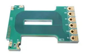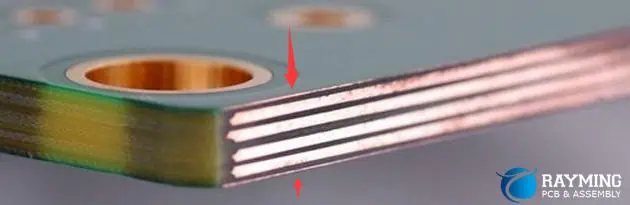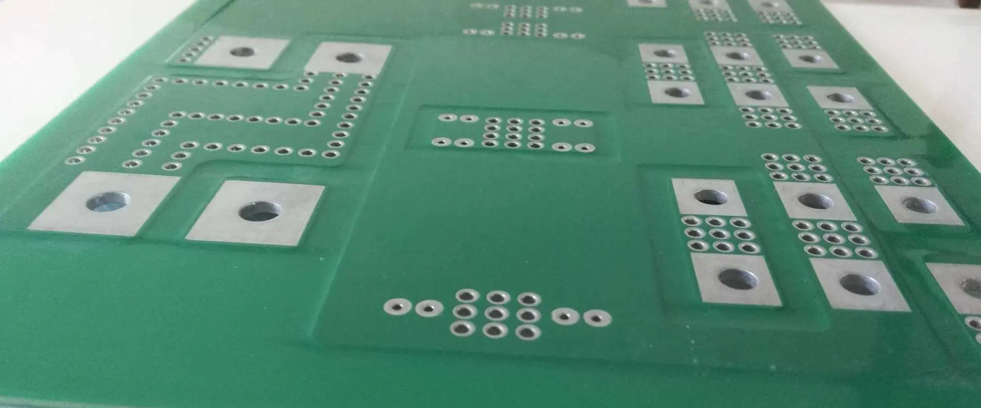
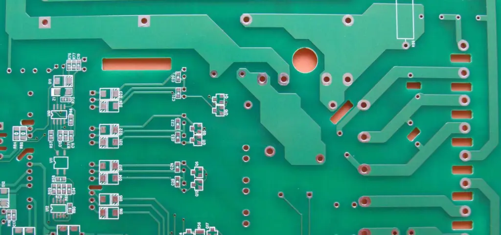
20 OZ Copper PCB

20 OZ Copper PCB
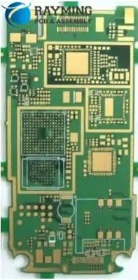
2 Layer PCB Board
Soler Mask : Green
Legent :White
Surface :HASL-LF
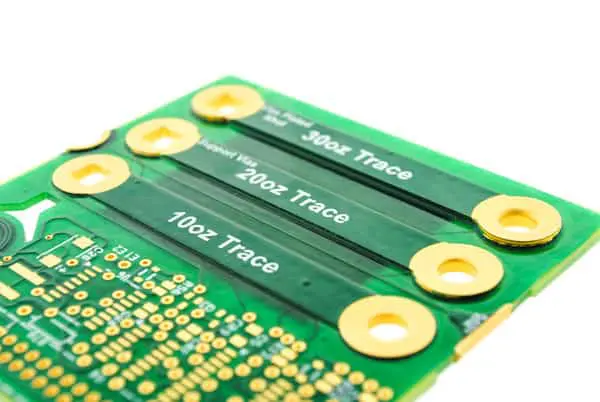
General Guideline for Min Spacing by Copper Weight
Cu Weight Min Recommended Space between Copper Feature
20 OZ 76mil ( 1.93mm)
Introduction
As power densities continue rising in advanced electronics, even thicker copper PCBs beyond 10 oz are being adopted. 20 oz copper printed circuit boards with extreme 700 μm (0.7 mm) foil thickness provide the utmost in performance. However, reliably producing 20 oz multilayer PCBs poses immense fabrication challenges. In this article, we examine the benefits of 20 oz copper boards, the stringent manufacturing capabilities required, potential applications, and key considerations when implementing this leading-edge PCB technology.
What is a 20 oz Copper PCB?
PCB copper thickness is measured in ounces per square foot (oz/ft2). This designates the weight of copper foil in one square foot of board area, excluding the dielectric substrate. Some standard copper weights are:
- 1 oz – 1 oz/ft2 (35 μm)
- 2 oz – 2 oz/ft2 (70 μm)
- 10 oz – 10 oz/ft2 (350 μm)
- 20 oz – 20 oz/ft2 (700 μm)
So a 20 oz copper PCB has 20 ounces of copper foil per square foot on each metal layer. In terms of thickness, 20 oz copper is approximately:
- 700 μm (0.7 mm)
- 28 mils
This extreme foil thickness enables the greatest power handling and reliability capabilities.
Benefits of 20 oz Copper PCBs
Some key advantages of 20 oz copper PCB technology include:
- Highest current capacity – Ability to sustain extremely high current loads without overheating due to massive copper cross-section.
- Lowest losses – Minimal resistive losses allow highly efficient power transfer and conversion.
- Finest thermal performance – The thick copper acts as a heat spreader keeping components cool.
- Superior shielding – Provides near total EMI isolation from thick uninterrupted planes.
- Extreme reliability – Highly resistant to thermal cycling, electromigration and physical stresses over decades.
- Low voltage drop – Negligible voltage loss along power distribution paths due to minimal resistivity.
- High power density – Maximum possible power can be delivered through a PCB footprint.
- Component integration – Embed heavy power components into 20 oz copper inner planes.
20 oz copper represents the leading edge of PCB material technology for the most extreme electrical and thermal demands.
Manufacturing Challenges with 20 oz Copper
Producing 20 oz copper multilayer PCBs poses immense fabrication difficulties including:
- Registration – Accumulated tolerance across over 0.7mm of copper can result in layer misalignments.
- Aspect Ratios – Plating extremely high aspect ratio holes of 28:1 is hugely challenging.
- Lamination Voids – Preventing any filler starvation areas or voids during bonding requires great precision.
- Surface Finish – Achieving uniform plating on coarse high copper weight foils is difficult.
- Fine Lines – Defining very fine traces on rough 20 oz foil surfaces poses issues.
- Layer Peel Strength – Very high adhesion between layers is needed to avoid any delamination risk.
- Via Filling – Pore-free copper plating of high aspect ratio holes demands special processes.
- Hole Wall Quality – Resin-rich smooth hole walls are essential to enable copper plating.
- Drilling – Straight vertical through holes without taper or breakage requires specialized drill bits and rigs.
- Panel Stress – Minimizing cumulative stresses and bow/twist during fabrication is critical.
These factors require highly mature manufacturing capabilities and controls to produce quality 20 oz PCBs reliably.
Key Manufacturing Capabilities for 20 oz Copper
To reliably fabricate 20 oz copper multilayer boards, PCB manufacturers must demonstrate several advanced capabilities:
- Registration Accuracy – Within 0.10mm between layers to prevent misalignment.
- Plating Aspect Ratios – Reliable copper plating down to at least 20:1 hole aspect ratios.
- Lamination – Use of high fillers in prepreg and precise pressure control during bonding.
- Etching – Fine line etching capability down to 1 mil line/space.
- Hole Wall Quality – Excellent resin coating of drilled hole walls with no pull-away.
- Surface Finish – Highly uniform thick gold plating over very coarse surfaces.
- Peel Strength – Interlaminar peel strength over 15 N/mm.
- Via Filling – Pore-free copper plating fill of high aspect through holes.
- Drilling – Straight vertical holes through >0.7 mm copper.
- Panel Flatness – Overall thickness variation under 5% with minimal bow or twist.
- Process Control – Mature statistical process monitoring and control systems.
These capability indicators validate whether a PCB company can reliably manufacture 20 oz multilayer boards.
Potential Applications of 20 oz Copper PCBs
Some examples of products that can utilize thick 20 oz copper PCB technology include:
- Electric vehicle powertrain – Motor controllers and battery management systems.
- Industrial power supplies – High capacity UPS and DC power systems.
- Heavy-duty motor drives – Drives for large electric motors and compressors.
- High power RF amplifiers – High frequency amplifiers for radio transmission.
- Power distribution – Switchgear, bussbars and junction boxes.
- Traction systems – Substations, converters and distribution for rail infrastructure.
- Power generators – Controls and distribution for power generators.
- Power converters – High capacity AC-DC and DC-DC converters.
- Renewable energy – Solar/wind power controllers and switching systems.
For such extreme high power applications, 20 oz copper provides the highest performance and reliability.
Implementing 20 oz Copper PCBs

For companies looking to utilize 20 oz copper PCB technology, key considerations include:
- Finding an established PCB manufacturer with proven 20 oz expertise. Their capabilities and experience are crucial.
- Leveraging the manufacturer’s guidance on design techniques optimized for ultra-thick copper.
- Budgeting for higher costs due to specialized fabrication processes required.
- Adjusting schematics for the lowest possible voltages and resistive losses.
- Planning for longer lead times due to process complexities.
- Testing initial prototypes extensively for power handling, thermal performance and reliability.
- Gradually optimizing designs based on initial builds before committing to volume production.
With careful planning and an expert partner, 20 oz copper PCB technology can enable unprecedented functionality in extreme high power electronics.
Conclusion
As electronics systems continue pushing the boundaries of performance and power densities, 20 oz copper PCBs with 0.7mm thick copper represent the state-of-the-art in PCB fabrication. They enable unmatched current capacity, thermal management and reliability. However, achieving flawless quality and yield requires mastering immense manufacturing challenges at scale. Partnering with an elite PCB company that has proven expertise in this highly specialized arena is key to mitigating risks and ensuring success when implementing leading-edge 20 oz copper PCB technology.