What is Xilinx XC7A200T-2FBG484i FPGA ?

Xilinx XC7A200T-2FBG484i

Introduction to FPGAs

FPGA stands for Field Programmable Gate Array. FPGAs are semiconductor devices that contain programmable logic blocks and interconnects that can be configured to implement custom hardware functionality. Unlike Application Specific Integrated Circuits (ASICs), the functionality of an FPGA can be changed and reconfigured by the designer after manufacturing. This makes FPGAs flexible and versatile for creating specialized electronics and accelerating processing in a wide range of applications.

Some key capabilities of FPGAs include:

  • Implementing digital circuits by interconnecting logic blocks
  • Reconfigurable even after deployment in the field
  • Supporting various interfacing standards and protocols
  • Embedding custom processors and intellectual property blocks
  • Prototyping designs before final ASIC fabrication

Leading vendors of FPGAs include Xilinx, Intel/Altera, Lattice Semiconductor, Microchip, and others. Designs are created using electronic design automation (EDA) software and a hardware description language like VHDL or Verilog.

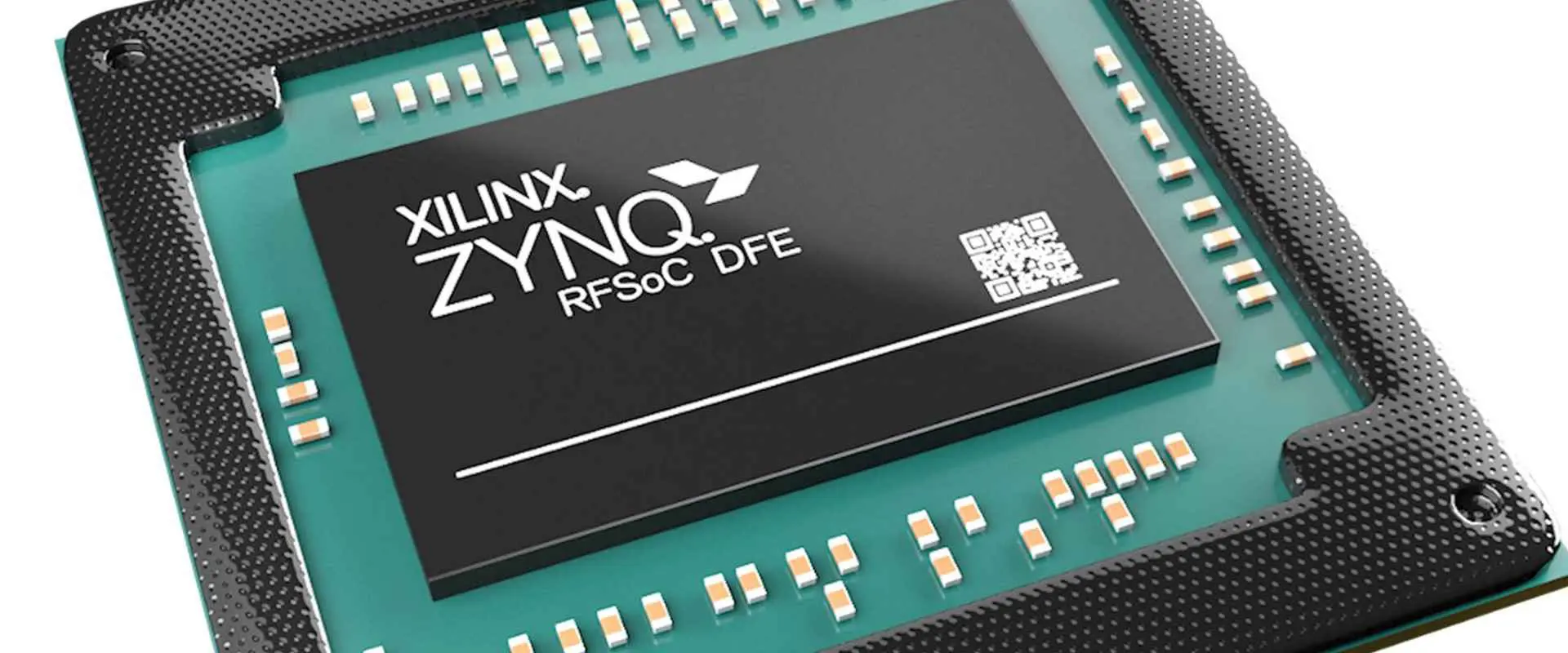
Introducing the Xilinx Artix-7 FPGA

The Xilinx Artix-7 FPGA series provides a cost-optimized programmable logic solution for high-performance system integration. The family spans from low-cost, small form factor devices to large, highly capable FPGAs for the most demanding applications. All Artix-7 FPGAs are based on the unified 28 nm high-k metal gate (HKMG) process from TSMC.

Key features of Xilinx Artix-7 FPGAs:

  • Built on 28 nm process with high density routing
  • High performance DSP blocks, block RAMs, transceivers
  • Low power optimization for power sensitive designs
  • High bandwidth with up to 17 Gbps transceivers
  • Leverages Vivado Design Suite for programming
  • Wide range of packages from 15K logic cells up to 215K logic cells

The Artix-7 series delivers an optimal balance of performance, flexibility and reduced power consumption. The devices enable emerging applications in fields like communications, data centers, aerospace, and industrial automation.

XC7A200T FPGA Overview

The Xilinx XC7A200T specifically belongs to the Artix-7 200T variant. Here are some of its key features:

  • 215,360 logic cells, each with a 6-input LUT and flip-flop pair
  • 20,150 Kbits of fast block RAM
  • 240 DSP slices with 25×18 multipliers
  • Six clock management tiles, each with phase-locked loop (PLL)
  • Eight receiver/transmitter blocks supporting up to 12.5 Gbps
  • Two PCI Express blocks
  • Two Ethernet MAC blocks
  • Advanced configuration like AES and CRC encryption
  • Multi-voltage, multi-standard I/O support
  • 1.0V core voltage, offering optimized low power

With these capabilities, the XC7A200T provides a high performance, power optimized FPGA well-suited for applications like wireless, wireline, broadcast, industrial motors, automotive driver assistance, video analytics, and aerospace and defense systems.

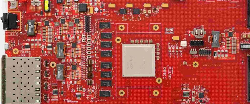
Details of the XC7A200T-2FBG484I Variant

The XC7A200T-2FBG484I is a specific package variant of the Xilinx Artix-7 XC7A200T FPGA. It has the following detailed characteristics and configuration:

  • 484 pin Flip-chip BGA (FBG) package
  • 1.0V core voltage
  • -2 speed grade, suitable for industrial temperature range
  • Operating temperature range of -40ยฐC to +100ยฐC
  • 27 x 27 mm package size
  • 1.1 mm ball pitch
  • 16 GT/s data transfer rate per differential I/O
  • 17 x 17 mm silicon die size
  • Pb-free RoHS 6 compliant part

This high-performance flip-chip package provides extensive I/O capabilities. The fine 1.1 mm ball pitch enables routing high pin count connections under the device. The industrial temperature range allows operation across a wide -40ยฐC to +100ยฐC ambient without degradation in performance.

FPGA Internal Architecture

Inside the XC7A200T FPGA, there are the following key functional elements:

Configurable Logic Blocks (CLBs)

  • The basic logic cell with a pair of 6-input LUTs and flip-flops
  • LUTs implement any 6-input logic function, flip-flops store data -215,360 CLBs in the XC7A200T FPGA

Block RAM (BRAM)

  • Dedicated memory blocks of 36 Kb providing fast access
  • Up to 20,150 Kb total BRAM in the XC7A200T

DSP Slices

  • Specialized blocks with fast 25×18 bit multipliers and adders
  • Allow high-performance digital signal processing
  • 240 DSP slices in the XC7A200T

Clock Management Tiles (CMTs)

  • Digital clock managers, jitter filters, frequency synthesizers
  • Six CMTs in the XC7A200T, each with a phase-locked loop

High-Speed Serial Transceivers

  • Eight serial transceiver blocks with up to 12.5Gbps data rates
  • Support variety of protocols including PCIe, Ethernet, Aurora

Routing Matrix

  • Interconnect matrix between logic blocks with various length lines
  • Provides extensive routing flexibility between components

In addition to these elements, there are abundant I/O resources, PCIe blocks, configuration logic, and other components.

Key Applications and Uses

The XC7A200T Artix-7 FPGA can be deployed in diverse applications including:

  • Wireless communication systems – 4G/LTE, 5G, Software Defined Radio
  • Aerospace and defense – Radar, imaging, ruggedized systems
  • Video broadcasting – Encoding, decoding, transcoding
  • Medical imaging – Ultrasound, MRI, tomography
  • Motor drives – Industrial, robotics, UAVs
  • ADAS and sensors – Vision systems, lidar, radar
  • Networking and telecom infrastructure
  • PCI Express and Gigabit Ethernet platforms
  • High speed data acquisition and analytics
  • Hardware acceleration for AI edge inference

For these systems, the FPGA provides low latency, real-time signal processing and control capabilities not achievable with microprocessors alone.

Design Considerations

Xilinx Kintex UltraScale FPGA Board

Some key considerations when designing with the XC7A200T FPGA include:

Power – Manage core, I/O and static power consumption especially in battery powered applications. Use power gating and low power design techniques.

Thermal – The FF484 package can dissipate up to 15W. Carefully model and monitor die temperature. Employ proper heat sinking.

Timing – Close timing margins impact performance. Optimize clock domains, I/O delays, and metastability.

Signal Integrity – Minimize noise through smart PCB layout and isolating analog/digital signals.

Radiation Hardening – Use mitigation techniques like TMR for aerospace and defense applications. The Artix-7 is not rad-tolerant by default.

Implementation Tools – Leverage Xilinx Vivado to fully optimize timing, resource usage, and power consumption.

Comparing to Other Xilinx FPGAs

Here is how the XC7A200T compares to some other devices in the Xilinx FPGA lineup:

FPGA SeriesProcessLogic CellsTransceiversDSP SlicesBRAMStrengths
XC7A200T28nm215K8 at 12.5Gbps24020MbLow cost, high capability
XC7Z04528nm218K16 at 28.05Gbps90027MbHigher performance
XC7V2000T28nm927K24 at 16.3Gbps2016174MbVery high density
XCVU37P16nm893K16 at 32.75Gbps2520145MbUltraScale performance
XCZU9EG7nm1.6M112 at 58Gbps5520307MbLeading edge UltraScale+

The mid-range Artix-7 XC7A200T balances capabilities and cost-effectiveness. Other families scale higher or lower depending on application needs.

Conclusion and Summary

The Xilinx XC7A200T-2FBG484I is a high-performance Artix-7 series FPGA manufactured on a 28nm process. The device contains 215K logic cells and abundant DSP, memory, transceiver, PCIe, and networking resources. The flip-chip 484-pin BGA package provides extensive I/O in a compact footprint. With low power consumption across an industrial -40ยฐC to +100ยฐC temperature range, the XC7A200T FPGA enables advanced signal processing, control, and accelerated workloads in demanding environments and applications ranging from aerospace to 5G communications. Engineers can leverage the flexible programmable architecture and Vivado design tools to rapidly develop and iterate customized implementations.

Frequently Asked Questions

Q: What type of FPGA is the Xilinx XC7A200T?

A: The XC7A200T is part of the Artix-7 family, which is a low-cost, high-capability 28nm FPGA series from Xilinx.

Q: What is the difference between XC7A200T and other Artix-7 FPGAs?

A: The XC7A200T has the highest density and performance in the Artix-7 lineup, with 215K logic cells and features like PCIe, GigE MAC blocks and 12.5Gbps transceivers.

Q: What package is used on the XC7A200T-2FBG484I?

A: It uses a 484-pin flip-chip ball grid array (FBG484) package capable of very high I/O bandwidth.

Q: What design tools can program the XC7A200T FPGA?

A: Xilinx’s Vivado Design Suite is used for IP integration, synthesis, place-and-route, and configuration.

Q: What are some target applications of the XC7A200T FPGA?

A: Wireless communications, motor drives, video broadcasting, aerospace and defense systems, medical and industrial imaging, and network infrastructure.

What is Red PCB ?

red circuit board

To comprehend the colors of PCB, we must be conscious that the coloring on a PCB is not the true color of the initial circuit. It’s a layer on the substance of the FR-4 PCB. The color observed on each board is due to the solder mask color, which shields the pure conductors on the panel.

The solder mask or copper oil color choice should be so high that it contrasts well with the top copper wires, and they can be identified readily. The colorful layer prevents the copper cables from short circuits. It also forms a protective layer against ordinary wear and scratches caused by extreme weather stress or any other potential cause for board deterioration.

A red PCB color code is normally used to distinguish the circuit from other boards. The main objective of adopting a red PCB color code is to recognize any specific component in a collective assembly.

Introduction:

The PCB color specifies the soldering oil or solder mask color. It comprises lacquer infused with colors known to preserve the exposed copper traces. The final color of the PCB is manufactured by mixing โ€“ epoxy, resembling the solder mask. Preventing short circuitry is one of the major uses of the solder mask.

What is Red PCB?

The hue of the red PCB solder mask is usually courageous and competent. There is quite a significant distinction between planes, voids, and traces.

Contrast is reduced, unlike the green PCB. Any amplification is used to check the traces of the board in the event of faults. It should be mentioned that the silkscreen is well-known for residual fluxes against the red backdrop. While red appears lovely, beautiful, and strong, green is still the finest.

Advantages of Red PCB:

Red PCB

Red PCBs enables you to connect all these aspects and use copper paths rather than wires so that comparatively tiny modules and wire saving are comfortable to control.

ร˜ Easy to repair:

If your Red PCB does not function reliably, the boards can be repaired very easily. That’s because the elements are easily checked and repaired, as all capacitances are labeled with a silkscreen on the panel. It not only makes the structure comfortable but also the consensus model.

ร˜ Time Saver:

The traditional method of creating circuit boards takes a lot of time. But the red PCBย not only requires less effort to use the printed circuit boardโ€™s technique but is much more useful.

ร˜ Fixed components:

During the construction of the electronic components, all of the modules are connected to the board and properly fastened. This is completed by solder flux that does not allow migration to dislocate the parts.

ร˜ Lesser chances:

All connection is established by copper and metal conductivity rails. There is indeed less chance of losing connections which can outcome in the board being short-circuited.

ร˜ Electronic noise reduction:

The red PCBs are so created that electronic noise can be hardly detected. Any disturbance in the presence of energy or radioactivity is discharged. A properly designed PCB gives noise. This is because the elements are so arranged that the distance sizes are very close to zero, and thus the radioactivity and EM ripples are relatively low.

ร˜ Lower price:

While most PCBs are established on computerized systems, the template concept design can be saved and used repeatedly when needed. Therefore, you can save time and money on many lots of extremely similar red PCBs at once.

Other Colors of PCB’s:

Before seeing the red PCB now, we will know about the various color options available for the Circuit board. The usual color of PCB is the green overlay. However, the color of PCBs is altering with the emergence of significant innovation and technical progress. In the latest days, most assemblies have pushed the usage of different colors rather than green PCBs. The below are some reason behind choosing apart from green-colored PCBs:

  • Using various PCB colors offers a clear sign of the changes in iteration to inform users.
  • Brightness or reduction will be achieved by using colors apart from green. You have to realize that assembly material is important due to transmission, absorption, and light reflection.
  • Different colors assist in avoiding different sorts of faults in a combined assembly. The choice of color kinds in comparison also benefits from the identification of result meetings.

The colors utilized to make PCBs include yellow, red PCB, black, white, blue, etc. PCB colors are often referenced as color codes for PCBs. Some current PCB types have adopted specific colors. The PC boards, for illustration, are still made of green epoxy.

The colors of the solder masks don’t influence the functioning of the PCB. However, the proven approach will be varied if various PCB colors are used. Contrastingly, blue and red hues like yellow and black mimic green PCB density with a slightly lower resolution. It should be emphasized that solder masks are very committed with clear visibility.

Colors of the solder mask:

Different varieties of solder mask colors have been shown. When combined, chromium and carbon generate a dark solder mask. The existence of carbon is conducive to this sort of solder mask. Leading layers are produced via PCB traces but may be utilized as a shield to isolate signals from diverse external sounds.

The black solder mask is very pricey, produced from a cobalt combination. Like most Optoelectronic devices, you will find simple PCB color codes. The blue solder mask is usually seen in LCDs. It is utilized to prevent any interruption in the system.

A red PCB color code is normally used to distinguish the circuit from other panels. The main objective of adopting a red PCB color code is to recognize any specific component in a bunch assembly. Red solder mask is usually utilized in precise equipment such as oscilloscopes, analog resources, and voltmeter bench.

Green is regarded as the popular color for printed circuit boards from several sources. This is because the green color performance is superior to other PCB colors. Green produces better outcomes when connecting the element pitch. Green is typically believed to be the default color for printed circuit boards.

Types of Colors in PCB:

If you are ready to pick the printed boards, various criteria must be taken into account. One of them is to choose the PCB solder mask color. Although green is the most typical hue, there’s no additional price for other colors, such as yellow, red, black, and white, that are also possible. Because the PCB solder mask has a wide variety of colors accessible, the challenge is which color has to be picked. Does the choice of color other than green have any benefits or downsides?

The brief instructions below will help you choose a different color from the typical green hue of the solder mask:

ร˜ Blue PCB:

PCB in blue color mimics the very same Arduino blue for the solder mask. The distinction between vacant areas, surfaces, and traces are modest compared with yellow and white printed circuit boards. In the color of the blue solder mask, magnification is regarded as essential and required for inspection of production flaws.

However, the disparity between the solder mask and the silkscreen can be observed as pretty great, utilizing the blue color. So if you use a label board, hefty, then the correct option may be blue for you in this scenario.

Remember that blue appears to be a great option if you’d like to combine the solder mask color with your Arduino.

ร˜ White PCB:

If you believe that it is the most difficult to manage a black solder mask, you haven’t seen white yet. Results revealed that a white solder mask is not acceptable. The contrast between white PCB and black is even worst. Even turning it to illumination does not assist with the appearance of its traces while examined. The white PCB is very difficult to clean since suggestions are difficult to spot. However, with white solder masks, the silkscreen intensity is the same as in black, which means they function quite well. Because of other characteristics, the white solder mask is not recommended.

ร˜ Black circuit board

One of the most complex integrated circuits is the black circuit board. It is nearly hard to distinguish between empty areas, lines, and traces using the blackboards. You must thus tilt the board over a light beam to check it.

Though on the other side the electrodes are extremely clearly defined if they work with a unique silkscreen. It enables the identification of spots easier but also designated accurately.

Apple is renowned for adopting black PCBs for its iPhones and MacBook boards.

ร˜ Yellow PCB

The yellow circuits are excellent and why most manufacturers don’t choose their solder mask color is still an astonishment. Yellow provides a more detailed contrast among empty areas, trails, and planes. It’s indeed comparable to the green color mask with a simplistic approach to use.

ร˜ Purple circuit board:

The purple hue is not a conventional or typical color on a PCB. You may be asked to pay a surcharge for this color option based on your fabricator. The contrast is great with the purple PCB, and the general workability is increased.

Final Thoughts

We are certain that you’ve just completely grasped why the Integrated circuit has several colors and why the green color is the most frequent of all. We also feel that we have addressed all your problems and issues with the various PCB colors.

In this respect, please contact us for all of your PCB color quotes, and we will assist you to cover your circuitry in a color of your choice.

What is a Blank Printed Circuit Board (PCB)?

blank printed circuit board

Introduction to Blank PCBs

A blank printed circuit board (PCB) refers to a PCB substrate that contains no components and has not yet been etched with conductive copper tracks or holes. It serves as the foundation for assembling a populated finished PCB assembly.

Blank PCBs consist of an insulating substrate material such as FR-4 with layers of laminated copper foil. The blank board has no circuit patterns yet. The copper layers will be chemically etched later to form the desired conductive paths between holes and pads based on the PCB design.

Reasons for Using Blank PCBs

There are several reasons why starting with a blank PCB is preferred for manufacturing PCB prototypes and production runs:

  • Cost – Pre-etched blank PCBs in bulk are cheaper than fully-assembled PCBs
  • Customization – Allows custom etching of traces for each unique design
  • Quality – Consistent base materials and copper layers
  • Efficiency – Specialized PCB fab houses can rapidly etch at scale
  • Flexibility – Soldering components to blank PCBs allows modifications

Blank PCB materials produced in high volumes optimize costs. Specialized PCB manufacturers can rapidly etch the blanks using automated processes. This allows great flexibility for engineers or hobbyists to iteratively assemble components and modify their circuits during development.

Blank PCB Manufacturing Process

Shengyi S1600 pcb

The typical manufacturing process for creating blank PCBs involves:

Substrate Materials Prep

  • Select PCB substrate (FR-4, polyimide, etc)
  • Choose dielectric thickness (1.6mm, 2mm etc)
  • Cut layers to desired PCB size and shape
  • Clean and prepare surfaces of materials

Layer Bonding

  • Take copper foils (1โ„2 oz, 1 oz thickness)
  • Arrange alternating PCB substrate and foil layers
  • Glue layers together under heat and pressure
  • Multiple layers bonded for multilayer PCBs

Surface Treatment

  • Apply photoresist coating over copper layers
  • Coat layers with tin, gold or other finishes
  • Electroplate nickel/gold edge connectors (optional)
  • Protective sealants applied on surfaces

Drilling Holes

  • Import drill files specifying hole sizes and locations
  • Precision-drill holes with CNC machines
  • Deburr holes to remove rough edges

Solder Mask Layers

  • Apply solder mask over entire PCB surface
  • Expose areas needing soldering later
  • Protects copper traces from oxidation and shorts

This creates blank double-sided or multilayer PCBs ready for custom etching. The blank PCBs provide the base foundation to then produce the finished populated PCB assembly.

Common Applications of Blank PCBs

Some typical applications where blank PCBs are used include:

  • Prototyping – Iteratively testing circuits using blank prototyping boards
  • Custom designs – Creating fully custom PCBs etched uniquely for each product
  • Medium volumes – Small and medium scale PCB production batches
  • Final product – Blank PCBs etched to produce the final PCB assembly
  • Repairs/rework – Blanks used for modifying and fixing PCB assemblies
  • Testing – Engineers debugging circuits on blank boards before final etching
  • Education – Learning PCB design using blank boards for experimenting

The flexibility of assembling circuits on blank PCB substrates makes them useful across many contexts from hobbyists to large-scale electronic devices production.

Types of Blank PCB Materials

Rogers TMM 10i Laminate

There are various options for the base substrate material used to manufacture blank PCBs:

FR-4

  • Most common and cost-effective material choice
  • Composite of woven fiberglass cloth with an epoxy resin binder
  • Flame resistant grade with high mechanical strength
  • Used for simple low-frequency consumer electronics PCBs

CEM-1

  • Woven cotton paper base impregnated with epoxy
  • Low dielectric constant and loss factor
  • Strong physical and electric properties
  • Good thermal endurance and insulation

Polyimide

  • Flexible substrate material available as sheets or tapes
  • Withstands high temperatures
  • Used for flex PCBs in wearable devices, robotics, aerospace applications

Rogers Materials

  • High frequency circuit laminates with advanced dielectric properties
  • Low signal loss even at high frequencies
  • Good thermal management
  • Common in RF and microwave PCBs

Ceramic Boards

Others

The substrate material depends on mechanical, electrical and thermal needs of the target application. Cost is also a major factor.

Key Characteristics of Blank PCBs

Some key characteristics and parameters to consider for blank PCB materials:

  • Dimensions – Overall PCB size, thickness, layer counts
  • Dielectric constant – Affects signal propagation through substrate
  • Loss tangent – Heat dissipation factor, affects high freq losses
  • Copper thickness – Determines current capacity and track resistance
  • Weave styles – Fiberglass weave pattern, affects flexibility
  • TGlass – Glass transition temp, maximum operating temp
  • CTE – Coefficient of thermal expansion
  • Moisture absorption – Affects electrical properties and dimensions
  • Hole walls – Copper thickness in holes during drilling
  • Edge connections – Nickel/gold plating on edges

Understanding these parameters helps select suitable blank PCB stock for the electrical, thermal, and mechanical needs of the circuit application and environment.

Key Considerations When Sourcing Blank PCBs

Isola FR408HR PCB

Some important factors to consider when choosing a blank PCB supplier:

  • Quality: Consistent quality and precise fabrication is crucial
  • Capabilities: Range of PCB sizes, layer counts, substrate materials supported
  • Volume pricing: Cost savings from high volume blank PCB production
  • Lead times: Fast turnaround enables rapid prototyping iterations
  • Testing and QC: Rigorous quality control to validate materials and dimensions
  • Certifications: ISO 9001 and other certifications
  • Reliability: Stable long-term source for production runs
  • Customer support: Help with design questions, issue resolution
  • Environmental compliance: RoHS, REACH compliance
  • Shipping and logistics: Handling of shipping, customs, and local delivery

Sourcing from reputable PCB manufacturers with experience delivers quality blanks suitable for surface etching to precision requirements.

Pros and Cons of Starting with Blank PCBs

ProsCons
Cost effective for medium to high volumesAdditional etching step required
Consistent base material qualityNeed separate soldering of components
Rapid, optimized fabrication in bulkHarder modifications or rework after etching
Flexibility to create many custom designsMore effort than using pre-made PCBs
Full control over circuit patternsCannot quickly test circuits before etching
Easier to update and modify prototypesRequires careful planning of layout before etching
Enables small scale in-house etchingLimited options for extremely low volume

Trends and Developments in Blank PCBs

Some current trends shaping blank PCB substrate materials and fabrication:

  • Continual improvements in consistency and maximum PCB sizes from new manufacturing techniques
  • Focus on environmentally friendly processes and conformance to standards like RoHS
  • Rising demand for high frequency, high density designs requires advanced materials
  • Miniaturization requires thinner dielectric substrates
  • Growth in multilayer boards with 20, 30 or more layers
  • Innovation in ceramic substrates like LTCC (low temp co-fired ceramic)
  • Additive manufacturing and nanoparticle inks enabling printed electronics
  • Increased simulation and modeling to validate electrical, thermal and mechanical properties

These advances are enabling blank PCB substrates with finer geometries and improved electrical and thermal characteristics.

Etching Process for Blank PCBs

The general PCB etching process flow to convert blank PCBs into finished boards with desired circuit patterns is:

PCB Design

  • Create schematic and layout in EDA software
  • Specify trace widths, clearances, pad shapes needed
  • Export Gerber and drill files

Imaging

  • Apply photoresist coating on blank PCB surface
  • Expose selective areas using UV light and film masks
  • Develop to remove exposed or unexposed resist areas

Etching

  • Immerse boards in chemical etchant solution
  • Etchant dissolves exposed copper to create traces
  • Different methods like cupric chloride or ferric chloride etching

Stripping and Finishing

  • Strip away remaining photoresist
  • Clean away etching residue on boards
  • Tin, silver, or gold plating of finished copper tracks

This subtractive process removes unwanted copper from the blank PCBs to produce the desired conductive circuit patterns.

Frequently Asked Questions

Arlon 38N pcb

Q: What are blank PCBs made of?

A: Blank PCBs consist of an insulating substrate material like FR-4 with layered copper foils. The substrate provides the base foundation and copper layers are etched to form circuit traces.

Q: Where can I get blank PCB boards manufactured?

A: Many online PCB manufacturers offer fabrication of blank PCBs in various sizes and materials. This allows purchasing them in volume for cost savings.

Q: Can I solder components on blank PCBs?

A: Yes, blank PCBs can have electronic components soldered on them. This allows assembling and testing a circuit before final etching of the copper layers.

Q: How are traces created on blank PCBs?

A: Traces and pads are formed on blank PCBs by a chemical etching process. A mask shields certain areas and etchant dissolves exposed copper to create the desired circuit pattern.

Q: When is it better to use blank PCBs vs pre-etched PCBs?

A: For custom or frequently changing designs, blank PCBs allow flexibility to etch unique PCB designs. For mass production of standardized boards, pre-etched PCBs may have time and cost advantages.

Conclusion

Blank printed circuit boards provide a cost-effective foundation for assembling custom PCBs in medium to high volumes. Starting with quality blank materials enables optimized fabrication techniques like chemical etching to rapidly produce the copper layer circuitry needed. With attention to substrate parameters and etching processes, blank PCBs can be transformed into fully functioning circuit boards tailored for an application. The flexibility makes them ideal for prototyping, testing, and small batch manufacturing.

Xilinx XC7a50T-2FGG484i:he Integrated Circuit Board with Embedded FPGAs

Xilinx XC7a50T-2FGG484i

Xilinx XC7a50T-2FGG484i is an integrated circuit board that uses embedded Field Programmable Gate Arrays (FPGAs) to aid the design and reconfiguration of different electronic devices.

It is one of the popular FPGAs in the Xilinx Artix-7 Family.

This article details everything you need to know about these gate arrays, as well as some of the features.

The Background

We would like to talk a bit about the background of these gate arrays. It is one of the series released under Xilinx Artix-7.

Like other Artix-7 FPGAs, the XC7a50T-2FGG484i is one of the cost-effective because it uses both AMS integration and DSP processing.

It also features transceiver line rates and higher performance-per-watt fabric used for optimizing the costs and improving efficiency.

Features of the XC7a50T-2FGG484i FPGA

What are those features that make XC7a50T-2FGG484i one of the best Field Programmable Gate Arrays (FPGAs) be categorized under the Artix-7 Family?

We are about to show you some of them. These features cut across different important metrics, such as power, cost reduction, and improved technology.

Cost Reduction

Reducing cost is very essential because designers and re-programmers do not want to spend more money when fine-tuning a circuit board.

That is why the different cost reduction mechanisms used on the XC7a50T-2FGG484i FPGA are impressive.

Here are some of the ways you can maximize the cost reduction of this board:

1. AMS Integration

The board integrates AMS, which combines with the DSP processing to deliver a fully cost-effective design.

Besides, the board supports 1,066Mb/s DDR3 support, which is powered by the MicroBlaze soft processor.

2. Mixed Signal Integration

The board also features analog mixed-signal integration, as well as low-cost, lidless flip-chip package options that make it truly affordable.

Power Considerations

The power considerations are also one of the innovative features of the XC7a50T-2FGG484i FPGA. It is common knowledge that Field Programmable Gate Arrays (FPGAs) process a lot at the same time.

So, it is impressive to see that this gate array is doing something different to address excess power consumption.

Here are some of the power-sensitive features on the XC7a50T-2FGG484i:

1. Ideal for Sensitive Markets

The board can be used across different markets, including markets that are particular about power. This is because of the combined size, weight, power, and cost (SWaP-C) demands.

In light of that, the XC7a50T-2FGG484i can be used in some of the power-sensitive markets including Communications and Avionics.

It is also ideal for some other power-sensitive applications, such as:

  • Low-end wireless backhaul
  • Software-defined radio
  • Machine vision cameras

The XC7a50T-2FGG484i is also designed to work optimally, irrespective of the applications. For example, it can be optimized for low-power applications that require Logic throughput, serial transceivers, and high DSP.

2. Power Reduction

As much as the gate array can be optimized to work in different applications, there may also be a need to reduce the power.

In such a case, the gate array will release the total power reduction feature that reduces 50% lower power and 65% lower static than 45nm generation devices.

Overall Performance

What is the performance level of the XC7a50T-2FGG484i? The performance of this gate array is facilitated in different ways.

Here are some of the metrics for judging the performance level:

1. State-of-the-art Performance

The improved performance of this gate array is possible because of the 28nm High-k Metal Gate (HKMG) technology. This technology works well even under Low Power (HPL). That way, power wouldnโ€™t be excessive, and the gate array will function as it should.

2. SelectIO Technology

The XC7a50T-2FGG484i also uses the high-performance Select IO Technology that supports DDR3 interfaces that can be as high as 1866Mb/s.

3. Powerful CMT

The gate array also prioritizes the Clock Management Tiles (CMT), which is why it is combined with the mixed clock manager and phase-locked loop.

Programmable System

The Artix-7 architecture also makes it easier to program the system integration on XC7a50T-2FGG484i. The programmed integration does not only increase the system performance. It also reduces the cost of the Bill of Materials (BOM).

Variety of Configurable Options

The XC7a50T-2FGG484i can also be configured into different options. Some of the options are:

  • Commodity memories
  • 6-input Lookup Table Technology
  • User-configurable analog interface

Design Productivity

The XC7a50T-2FGG484i also has a productive design. At the core of the productivity is the scalable optimized architecture that can be fine-tuned to fit into a variety of purposes.

The accelerated design productivity also includes comprehensive tools and IP.

Here is the additional design productiveness of the XC7a50T-2FGG484i Field Programmable Gate Arrays (FPGAs).

1. Speed

The speed of this gate array is facilitated in many ways. The most common is the 1.2V to 3.3.V I/O voltage, high-speed serial connectivity that comes with built-in gigabit transceivers.

The second aspect of the speed is the -3, -2, -1, -1L, -2L speed grade options. These speed grade options also come with up to 100 degrees Celsius temperatures.

2. Logic Cells

The 215K Logic Cells also play a vital role in the accelerated speed of the gate array. The logic cells work alongside the 740 DSP slices, 929 GMAC/s, 13Mb BRAM, and 16 transceivers that can have up to 6.6 GB/s transceiver speed.

The speed of the gate array also includes important features, such as x4 Gen2 PCIe interface and 500 I/O Pins. It also includes 211 GB/s serial bandwidth.

Security Architecture

For the XC7a50T-2FGG484i FPGA to function optimally, it needs to have relevant security architecture or a valid means of authentication.

That is not missing because the gate array has the 256bit AES encryption that doubles the security layer with the HMAC/SHA-256 authentication.

The security architecture is tripled by the SEU detection and correction feature.

With those in place, designers will be confident using the XC7a50T-2FGG484i because the security has been secured from all angles.

Wrapping Up

Field Programmable Gate Arrays (FPGAs) can make your reprogramming or reconfiguration job easier. You just need to get the right board for the job.

The XC7a50T-2FGG484i is all shades of what an ideal FPGA should be. From speed to improved security and better performance – it has it all.

What is Rogers RO4534 PCB ?

Rogers RO4534

The Rogers ro 4534 are performance/cost materials manufactured and engineered to meet the demands and needs of the antenna markets. This laminate extends the abilities and capabilities of the RO 4000 into the antenna applications.

This glass-reinforced, ceramic-filled material offers low loss performance, controlled dielectric constant, and great passive intermodulation response, which is necessary for applications working for mobile infrastructure microstrip antennas.

The rogers ro4534 laminates are very compatible with lead free high-temperature solder processing and conventional FR4. These laminates donโ€™t need any special treatment required on PTFE-based traditional laminates. This product is a cheap option to antenna technologies that are more conventional, thereby giving the designers the opportunity to maximize the performance and price of their antennas. Moreover, these materials come halogen-free, helping them meet the very strict โ€œgreenโ€ standards.

More Information about the Rogers RO 4534

The ro 4534 dielectric materialsโ€™ resin systems were designed to offer the needed properties for an optimal antenna performance. The CTEs โ€“ Coefficient of Thermal Expansion in both directions X and Y share similarities to that of copper. This great match in CTE helps in reducing stresses in the antenna of the printed circuit board (PCB).

The temperature of the typical glass transition of roger ro4534 materials surpasses 280 degrees centigrade, which leads to a low CTE on the z-axis and well-plated via hole reliability. Combining these properties with a dimensional stability value below 0.05% ensures that the ro 4534 laminates are great for PCB antenna applications. These materials also offer increased thermal conductivity, which ensures antenna designs that have increased power handling capability.

Asides from these great thermo-mechanical properties, the ro4534 laminates have electrical properties that designers of antennas need. The dielectric constant of these laminates ranges from 3.3 to 3.5. Measured at 2.5 GHz, it also has a loss tangent of 0.0020 โ€“ 0.0037. With these values, antenna designers will be able to realize great gain values coupled with reducing signal loss. These materials come with low PIM performance. Using two swept tones of 43 dBm at 1900 MHz, they have better values than -155 dBC.

Exposing these materials for long hours in any oxidative environment will alter the dielectric properties of the materials. At higher temperatures, the change rate increases, and it greatly depends on the design of the circuit. Although the high frequency materials of Rogers have been used in many applications and oxidation reports which led to performance issues are very rare. Roger has advised that all customers evaluate the design and material combination properly, to help in determining fitness for use over the end productโ€™s entire life.

Features of the ro4534

  • Loss range: 0.0020 to 0.0037
  • Dk range: 3.3 to 3.5
  • Thermoset resin system
  • Great dimensional stability
  • High thermal conductivity
  • Mechanical properties are uniform
  • Low PIM response

Applications

  • WiMAX antenna networks
  • Cellular infrastructure base station antennas

Properties of Rogers RO4534

Rogers RO4534 pcb

The properties of the rogers ro4534 are:

Coefficient of Thermal Expansion

This is also represented as CTE. This helps in measuring the rate at which the ro4534 expansion occurs whenever it is heated up. It is expressed in ppm (parts per million), and measured in PPM/oC. Once there is a risen in the materialโ€™s temperature which is higher than the Tg, then the CTE will also increase. The ro4534 has a high coefficient of thermal expansion.

Thermal Conductivity

Thermal conductivity can be represented as k. This property reveals the ability of the material to conduct heat. Whenever this value is low, the there is a low heat transfer, and when it is high, then there is a high heat transfer. The unit of measurement of this property is Watts/meter Kelvin.

Glass Transition Temperature

This property can be represented as Tg. This is the temperature where the substrate changes into a soft state from its initial rigid and glassy state. Measurement is usually done in degrees Celsius.

Decomposition Temperature

This temperature is one at which the material will decompose chemically. Its unit of measurement is degrees Celsius.

Dissipation factor (Df) or Loss Tangent

This is the tan of the phase angle. This is between the resistive and the reactive currents of the dielectric. A rise in dielectric loss happens whenever there is an increase in the dissipation factor. ย A low dissipation factor provides fast substrates, while large ones deliver slow substrates.

What to do when Choosing the Rogers 4534

You should consider some things when choosing the rogers ro4534:

Check that the Coefficient of Thermal Expansion matches: The coefficient of thermal expansion has proved to be very significant when handling substrates. Difference in the rates of the coefficient of thermal expansion reveals that during the fabrication process, expansion will take place at different rates.

Materials Chosen Should Have Similar Dielectric Constant: Ensure you go for substrates having dielectric constants that are identical.

Choose Flat and Tight Substrate Weaves: Achieving this ensures you have high-frequency and high-speed usages. This feature also ensures the dielectric constant is distributed evenly.

Choose Materials with Low Moisture Absorption: Moisture absorption deals with the resistance of the PCB material when inserted into water. The weight of the PCB will increase as you get the material absorbed in water.

Donโ€™t Make Use of FR-4 for Applications That Require High Frequency: Avoid this at all cost, because they usually have a high dielectric loss. Asides from this, the Dk is usually sharp anytime it is compared to the frequency response curve.

Benefits of Choosing RO4534

  • Suitable for different applications
  • Higher yield on panels with larger sizes
  • Improved power handling
  • Robust handling
  • Long life when used with thin materials

Conclusion

This glass-reinforced, ceramic-filled material offers low loss performance, controlled dielectric constant, and great passive intermodulation response. These laminates are very compatible with lead free high-temperature solder processing and conventional FR4. These laminates donโ€™t need any special treatment required on PTFE-based traditional laminates. This product is a cheap option to antenna technologies that are more conventional, thereby giving the designers the opportunity to maximize the performance and price of their antennas.

Why Are Most PCBs Green? The Science Behind Green Solder Mask & Circuit Board Material

Green PCB

When you think of a printed circuit board (PCB), what color comes to mind? For most people, it’s green. The iconic green PCB has become synonymous with electronics and technology. But have you ever wondered why green is the predominant color for these essential components? In this article, we’ll explore the fascinating world of green PCBs, delving into the science behind their color, the history of their development, and the practical reasons for their widespread use in the electronics industry.

What is a Solder Mask?

Before we dive into the reasons behind the green color, it’s essential to understand what a solder mask is and its role in PCB manufacturing.

Definition and Purpose

A solder mask is a thin layer of polymer applied to the copper traces of a printed circuit board. Its primary functions are:

  1. To protect the copper traces from oxidation
  2. To prevent solder bridges between closely spaced solder pads
  3. To insulate the board from environmental factors

Application Process

The solder mask is typically applied using a screen printing or photoimaging process. After application, it’s cured using UV light or heat, depending on the type of solder mask material used.

The History of Green PCBs

Shengyi SCGA-500 GF255 PCB

The use of green as the standard color for PCBs has an interesting history that dates back several decades.

Early PCB Manufacturing

In the early days of PCB production, boards were often left uncoated or were coated with a clear or yellowish epoxy resin. These boards were prone to oxidation and other environmental damage.

Introduction of Green Solder Mask

The green solder mask was introduced in the 1960s by the U.S. military. The specific shade, known as “military green” or “olive drab,” was chosen for its ability to meet certain visual and functional requirements.

Widespread Adoption

As the electronics industry grew, the use of green solder mask became increasingly common due to its effectiveness and the standardization of manufacturing processes.

The Science Behind Green Solder Mask

Green solder mask
solder mask

The choice of green for solder masks isn’t just about aesthetics. There are several scientific and practical reasons why green has become the industry standard.

Optimal Light Absorption for Exposure

One of the primary reasons for using green solder mask is its optimal light absorption properties during the manufacturing process.

UV Light Exposure

During PCB manufacturing, the solder mask is exposed to UV light to cure and harden it. The green pigment used in the solder mask has been found to absorb UV light effectively, ensuring proper curing of the mask.

Wavelength Considerations

The specific wavelength of light absorbed by the green pigment aligns well with the UV light used in the curing process, leading to consistent and reliable results.

Better Visibility for Inspection

Green solder mask offers significant advantages when it comes to visual inspection of PCBs.

Contrast with Copper Traces

The green color provides excellent contrast with the copper traces and other components on the board, making it easier for inspectors to identify defects or issues.

Reduced Eye Strain

The green color is also known to be easier on the eyes, reducing fatigue for workers who need to inspect PCBs for extended periods.

Material Composition

The composition of the green solder mask contributes to its effectiveness and durability.

Epoxy Resin Base

Most green solder masks are made from epoxy resin, which offers excellent adhesion to the PCB surface and resistance to environmental factors.

Pigments and Additives

The green color is achieved through the addition of specific pigments and additives to the epoxy resin. These additives not only provide the color but also contribute to the mask’s overall performance.

Read more about:

Are There Other PCB Colors?

While green is the most common color for PCBs, it’s not the only option available.

Common Alternative Colors

Other colors used in PCB manufacturing include:

  1. Red
  2. Blue
  3. Black
  4. White
  5. Yellow

Reasons for Different Colors

There are several reasons why manufacturers might choose a different color for their PCBs:

Aesthetic Considerations

Some companies opt for different colors to match their branding or to create a unique visual identity for their products.

Functional Requirements

Certain applications may benefit from specific colors. For example, white solder masks are often used in LED applications to improve light reflection.

Industry-Specific Standards

Some industries have developed their own color standards. For instance, many aerospace applications use blue PCBs.

Why Green Remains the Standard

Despite the availability of other colors, green continues to be the most widely used color for PCBs. There are several reasons for this:

Manufacturing Efficiency

Green solder mask has been optimized for the PCB manufacturing process over many years, leading to consistent and reliable results.

Established Processes

Many manufacturers have fine-tuned their processes specifically for green solder mask, making it the most efficient option.

Quality Control

The widespread use of green PCBs has led to well-established quality control standards and inspection procedures.

Cost-Effectiveness

Green solder mask is typically the most cost-effective option due to its widespread use and economies of scale in production.

Bulk Production

The high demand for green solder mask allows manufacturers to produce it in large quantities, reducing overall costs.

Standardized Equipment

Most PCB manufacturing equipment is optimized for use with green solder mask, making it a more economical choice for many companies.

Industry Familiarity

The long-standing use of green PCBs has created a sense of familiarity and trust within the electronics industry.

Engineering Expectations

Many engineers and designers are accustomed to working with green PCBs, making it easier to spot issues or anomalies.

Consumer Recognition

The green color has become synonymous with PCBs in the public eye, creating a sense of authenticity and reliability.

Environmental Considerations

In recent years, there has been growing interest in the environmental impact of PCB manufacturing, including the choice of solder mask color.

Eco-Friendly Alternatives

Some manufacturers are exploring more environmentally friendly solder mask options, which may impact color choices in the future.

Recycling Challenges

The color of PCBs can affect their recyclability, with some colors being more challenging to process than others.

The Future of PCB Colors

As technology advances and new materials are developed, we may see changes in the predominant colors used for PCBs.

Emerging Technologies

New manufacturing techniques and materials may lead to a broader range of color options or even color-changing PCBs.

Customization Trends

Increasing demand for product customization may drive more variety in PCB colors, especially for consumer electronics.

Conclusion

The prevalence of green PCBs is a result of a complex interplay of historical, scientific, and practical factors. The green solder mask has proven to be an optimal choice for PCB manufacturing due to its light absorption properties, visibility benefits, and overall performance characteristics. While other colors are available and may be chosen for specific reasons, green remains the industry standard due to its efficiency, cost-effectiveness, and familiarity within the electronics industry.

As we look to the future, it’s possible that advancements in technology and changing industry needs may lead to shifts in PCB color preferences. However, the iconic green PCB is likely to remain a familiar sight in the world of electronics for years to come. Whether you’re an electronics enthusiast, a professional engineer, or simply curious about the technology around you, understanding the science behind green PCBs provides valuable insight into the intricate world of electronic manufacturing.

What is PCB Milling ?

PCB Milling

The method of PCB milling is to remove copper portions from a surface of imprinted circuit board stuff to replicate pads, signal tracks, and designs from an electronic circuit board blueprint known as a designed to explain. The PCB milling process is simultaneous, like the more popular and widely known caustic PCB etch process: substance is removed to generate electric insulation and contact planes. But, unlike the synthetic etch process, PCB milling is a non-chemical procedure that may be done without exposure to dangerous chemicals in a regular office or laboratory setting. Circuit boards of high quality may be created using either technique. For PCB milling, the condition of the circuit board is controlled primarily by the service’s true or weighted visibility and accuracy of the milling, including its conditional sharpness, the temperature of the frame components, and their corresponding feed or rotating speed. In comparison, the integrity of a circuit board relies in the molecular etch process on the precision and efficiency of the cover used to shield copper towards chemical compounds and on the condition of etching chemicals.

YouTube video

Introduction

PCB milling is the process of metallic portions being removed from a board material pad. It should be accomplished if you want to design pads, frameworks, and lines of signals according to the digital circuit board. The PCB friction method permits the removal of materials to form electrical insulation and the necessary ground aircraft. The method does not entail the use of petro-chemicals and may be conducted in an office. This implies that the method does not introduce the environment to dangerous chemicals and enables an elevated circuit board.

Parameters of milling:

The tool diameter is the lowest 0.8 mm, the normal diameter 2,0 mm, the customized diameter >=0.8 mm<2.0 mm, but the internal and outside board contours are milled according to client requirements.

Following the client’s requirements, the outside contour maybe 90ยฐ and round, but the inside corner of the design has at minimum the milling cutter diameter. Usually, the edge of the rectangle orbits the earth; the matching milling portion should also be perforated at the sides to preserve a precise rectangular area.

The breakaway and contour of PCBs are usually machined. Whereas, certain rules exist:

  • Usually, there is no additional frying price.
  • With the copper endurance of the circuit board, the danger of harm must be avoided.
  • The inner and outside contours of the board should be marked with a channel length of 1ฮผm to avoid problems of measuring and size.

The Board’s quality:

It is vital to bear in mind that the board’s performance is defined by the visibility and accuracy of the milling and the sharpness of the frames. PCB friction enables prototyping and a unique Pcb layout. A solitary device may be used to conduct the operation necessary to make a prototype board during molding. For seamless operation, the equipment employs conventional Ac power and vacuum cleaner. The physics underlying the frying machine is simple. It’s small and precise. It is easy to manage the equipment through software using instructions delivered. The microcontroller should then monitor constituent location while the friction head moves. This enables to adjustment of the speed of the spindle from 30 000 RPM to 100 000 RPM. Note that the faster the speed of the spinning, the more exact it is.

The PCB Milling Machine uses the phase motor to drive accuracy for the X and Y coordinate mechanism. For coordination in the milling, a specific precision link assembly might be employed. Milling PCBs have several issues, including flatness variances. The rationale is because gravure methods employ optical traps on the copper foil that may be matched to the small bends in the substance used to guarantee that all characteristics are duplicated. However, as you mill, the small fluctuation in height enables con-shaped parts to sink or rise. Therefore, mapping might be essential to assist tune the Z-values in advance.

Important PCB milling processes:

CNC PCB milling
  • It will be milling in thirty minutes, but some elements affect it, such as the bit diameter, the size of the circuit board, quantity parts, and their alignment.
  • PCB fraying is how the surplus copper is removed from the circuit board to generate signal lines and routes based on the design process.
  • The PCB maker may provide you with PCB milling technology.
  • PCB framing may be done in a laboratory atmosphere and is free of harmful chemicals; as it is the actual non-chemical technique, it has a short runtime for various circuit boards.
  • The precision of milling and the milling bits’ hardness directly impact the PCB performance.
  • The quality and accuracy of the circuit board for the rotating velocity of frying bits seem to have little impact.
  • If you’re using the milling machine for the first time, you have to practice this technique of manufacturing PCB.
  • You can manufacture high-quality items with more accuracy if you can take certain steps before manufacturing the circuit board.
  • There are multiple software types, Raster & Vector.
  • Software that uses raster calculations is less processed than software based on vectors since it depends on the raster data.

What is the miller?

The mechanisms underlying a PCB fryer are extremely simple and rooted in CNC friction technology. The PCB friction system is analogous to a small and very precise NC friction table. During machine control, machinery control communication and knowledge instructions will be transferred from the monitoring systems through a serial port/parallel to get this to the onboard controller of the machine tool. The controller then drives and monitors the several placement elements which move the frame head and door and regulate the speed of the spindle. Spinner speeds may vary from 30 000 RPM to 100 000 RPM based on the milling system with faster spindle speeds equal to greater precision. This drive system typically includes unmonitored stepper motors for the X/Y axis, unmonitored, on-off solenoid, hydraulic piston or plumbing screw for the Z-axis, and a spindle speed DC motor control unit, none of which provides positioning feedback. More modern systems feature a controlled stepper Z-axis drive to improve the control across a larger range of temperatures during frying and piercing and more complex RF spindle motor control circuits.

Type of Tools for Milling Mechin:

As long as you generate appropriate Gerber and drill files for your PCB development tools, you’ll be prepared to produce GCODE prepared files for the CNC Finder. This phase may be readily done using general-purpose third-party technology that accepts typical Gerber photoplotter data as an interface. You will have the choice to designate multiple surface geometry for milling, cutting, or isolation milling once you operate inside this program. Parameters are also supplied that determine cutting heights and drill diameters and subsequently produce the GCODE for the CNC machine.

As a PCB developer, you want to have the optimal PCB system design for all possible established standards and configuration choices accessible to provide CNC prototype management information. Allegro PCB Creator is a CAD solution with tools that meet this need flawlessly. Allegro has a thorough and extensive number of design rules and limitations that allow you to fully manage all the spacing criteria for your next prototype board.

Milling VS Etching:

In general, chemical grafting requires film or direct laser imaging, although the grafting itself is very inexpensive and typical in the worldwide manufacture of printed circuit board systems.

Isolation milling does not require film art but creates high tooling costs and issues with the application. That’s why isolation milling is much more important for prototypes initially and individually.

No difficulty with etching as the FR4 carrier is not etched.

V-scoring impacts when two systems of isolation are upon one other.

Advantages of PCB milling:

Of course, PCB friction offers benefits for both manufacturing of PCBs and certain specific PCBs. As well as the circuit board does not have to manufacture chemicals that might be the largest benefit.

Firstly, you must take time to build a prototype. The alternative is to create inside a circuit board. There could, however, be some challenges with the disposal of chemicals utilizing the water technique for internal manufacturing. Even though the high-definition circuit boards are tough to produce using the wet method, they still have to drill and eventually cut the circuit board out from the base course.

On the other side, the prototype of CNC machines allows rapid turn PCB manufacturing with rapid lead time requiring wet processing. When a CNC machine has already been utilized for boiling, this single device might do both process sections: frying and cutting operation. In addition, for boiling, milling, and cutting, a CNC machine is employed.

Several circuit boards that are easy to grind by wet etching and hand boiling in a lab setting will have such a tough time, provided you don’t employ the top line equipment that normally costs many times more than CNC milling.

Although, CNC is now normal to practice for cutting the circuit boards for grafting in the mass manufacturing of PCB.

Illuminating Innovation: The Rise of White PCBs in Modern Electronics

white circuit board

White solder mask is a popular choice for metal-core LED PCBs, offering both optical and thermal advantages. When designing circuit boards for LED applications, engineers must balance two critical factors:

  1. Optimal Light Reflectionย โ€“ White solder mask enhances brightness by improving light diffusion, ensuring clean and accurate color rendering from LEDs.
  2. Efficient Heat Dissipationย โ€“ Since LED components generate significant heat, the reflective properties of white solder mask help manage thermal performance, especially when paired with metal-core substrates.

By improving both light output and heat management, white solder mask has become a key material in high-performance LED PCB designs.

Introduction

Printed Circuit Boards (PCBs) are the unsung heroes of our electronic devices, providing the foundation upon which all components are mounted and interconnected. For decades, the iconic green color has been synonymous with PCBs. However, as technology advances and design aesthetics evolve, white PCBs are emerging as a popular alternative, offering both functional and visual benefits.

What is a White PCB?

1 Definition and Composition

A white PCB, at its core, is similar to any other PCB in terms of its basic structure and function. The key difference lies in the color of the solder mask โ€“ the protective layer applied to the copper traces of the PCB. In white PCBs, this solder mask is, as the name suggests, white instead of the traditional green.

2 Manufacturing Process

The manufacturing process for white PCBs is largely similar to that of traditional PCBs. The primary difference occurs during the application of the solder mask. White solder mask is typically made from epoxy-based materials with added pigments to achieve the desired color and opacity.

Read more about:

Advantages of White Circuit Boards

White PCBs offer several advantages over their green counterparts, making them increasingly popular in various applications.

1 Enhanced Visibility

One of the most significant benefits of white PCBs is improved visibility. The white background provides a stark contrast to component markings, solder joints, and copper traces, making it easier for engineers and technicians to inspect, assemble, and troubleshoot boards.

2 Heat Reflection

White surfaces naturally reflect more light than darker colors. This property translates to better heat reflection in white PCBs, potentially leading to improved thermal management in electronic devices.

3 Aesthetic Appeal

In an age where design aesthetics are increasingly important, white PCBs offer a clean, modern look. This is particularly valuable in consumer electronics where the PCB might be visible, such as in transparent or translucent device casings.

4 Customization Opportunities

The white background of these PCBs provides an excellent canvas for custom designs, logos, or additional information to be printed directly on the board, enhancing branding opportunities.

Top Brands of White Solder Mask

Several manufacturers have developed high-quality white solder mask products to meet the growing demand. Some of the leading brands include:

1 Taiyo

Taiyo is renowned for its PSR-4000 AUS308 series, which offers excellent whiteness and stability.

2 Peters

Peters’ SD 2950 series is known for its high-performance white solder mask suitable for a wide range of applications.

3 Huntsman

Huntsman’s Probimer series includes white solder mask options that provide excellent coverage and durability.

4 Electra Polymers

Electra Polymers offers the EMP110 series, which includes high-quality white solder mask options.

Applications of White PCBs

white-pcb

White PCBs are finding their way into various applications across multiple industries.

1 LED Lighting

In LED applications, white PCBs enhance light reflection, potentially improving the overall luminous efficacy of LED products.

2 Medical Devices

The high contrast provided by white PCBs is particularly valuable in medical devices, where precision and ease of inspection are crucial.

3 Aerospace and Defense

White PCBs are gaining traction in aerospace and defense applications due to their heat-reflective properties and high visibility for inspection and maintenance.

4 Consumer Electronics

Many high-end consumer electronics, particularly those with transparent or translucent casings, are utilizing white PCBs for their aesthetic appeal.

5 Automotive Electronics

The automotive industry is adopting white PCBs in various applications, especially in lighting systems and display units.

Operation of Applying White Solder Mask

The application of white solder mask requires precision and attention to detail to ensure optimal results.

1 Surface Preparation

Before applying the solder mask, the PCB surface must be thoroughly cleaned and prepared to ensure proper adhesion.

2 Solder Mask Application

The white solder mask is typically applied using screen printing or photoimaging techniques. The choice depends on the complexity of the board and the required precision.

3 Curing Process

After application, the solder mask undergoes a curing process, usually involving exposure to UV light and heat treatment to achieve the desired hardness and durability.

4 Quality Control

Post-curing, the boards undergo rigorous quality control checks to ensure uniform coverage, proper thickness, and absence of defects.

7. Challenges & Considerations

While white PCBs offer numerous advantages, there are also challenges and considerations to keep in mind.

1 UV Sensitivity

White solder masks can be more sensitive to UV light, potentially leading to yellowing over time if not properly formulated or protected.

2 Cost Considerations

White PCBs may come at a slightly higher cost compared to traditional green PCBs due to the specialized materials and potential additional processing steps.

3 Optical Considerations

In some applications, the high reflectivity of white PCBs might interfere with certain optical sensors or components.

4 Manufacturing Complexity

Achieving a uniform, defect-free white surface can be more challenging than with green solder masks, potentially leading to higher rejection rates in manufacturing.

White PCB vs. Traditional Green PCB

Super white LED PCB
Super white LED PCB

To fully appreciate the impact of white PCBs, it’s essential to compare them directly with traditional green PCBs.

1 Visibility and Inspection

White PCBs offer superior contrast, making component markings, traces, and solder joints more visible. This can lead to easier assembly, inspection, and troubleshooting compared to green PCBs.

2 Thermal Properties

The higher reflectivity of white PCBs can contribute to better heat management in some applications, potentially offering a slight advantage over green PCBs in terms of thermal performance.

3 Aesthetic Considerations

White PCBs provide a modern, clean look that can be more visually appealing in certain applications, especially where the PCB is visible in the final product.

4 Manufacturing and Cost

While the manufacturing process is similar, white PCBs may require more precise control and potentially more expensive materials, leading to a slight cost premium over green PCBs.

5 Industry Adoption

Green PCBs still dominate the market due to their long-standing use and familiarity. However, white PCBs are gaining ground, especially in specific sectors like LED lighting and high-end consumer electronics.

Future Trends in White PCB Technology

The future of white PCB technology looks promising, with several trends emerging:

1 Advanced Materials

Research is ongoing to develop white solder mask materials with improved UV resistance, thermal properties, and durability.

2 Integration with Flexible and Rigid-Flex PCBs

As flexible and rigid-flex PCBs become more prevalent, we can expect to see white solder mask options for these advanced board types.

3 Enhanced Printability

Improvements in white solder mask formulations are likely to enhance the ability to print high-resolution text and graphics directly on the board surface.

4 Smart PCB Integration

As IoT and smart devices proliferate, white PCBs may play a role in integrating visual indicators or even display elements directly into the board surface.

5 Sustainability Considerations

Future developments may focus on creating more environmentally friendly white solder mask materials, aligning with the growing emphasis on sustainability in electronics manufacturing.

Conclusion

White PCBs represent a significant evolution in printed circuit board technology. Their enhanced visibility, aesthetic appeal, and potential performance benefits are driving adoption across various industries. While challenges exist, ongoing research and development are likely to address these issues, further solidifying the place of white PCBs in modern electronics.

As we look to the future, white PCBs are poised to play an increasingly important role in electronic design and manufacturing. Their ability to combine functionality with aesthetics makes them a compelling choice for innovators pushing the boundaries of what’s possible in electronics. Whether it’s in the next generation of LED lighting, cutting-edge medical devices, or sleek consumer electronics, white PCBs are illuminating the path forward in the world of electronic innovation.

What is Yellow PCB ?

yellow circuit board

The color of the PCB determines the color of the coating process or solder oil. It is made out of shellac that has been treated with colors considered to preserve exposed copper traces. The solder mask is represented by the final color of the PCB, which is prepared by mixing. Among the most common uses of the solder mask is to protect the PCB board from relatively brief.

Colors on PCBs come in a variety of shapes and sizes.

For the Circuit board, there seem to be a variety of colors to choose from. The green solder mask is the traditional color for circuit boards. The color of PCBs is evolving and growing with higher productivity and technical improvement. Most fabricators have propelled the growth in usage of various colors rather than green PCBs in recent times. The preceding are reasons why you may choose to go with a color other than green for your PCB.

The colors of solder masks have no effect or influence on the PCB’s functionality. However, the compliments will be varied if various PCB colors are used. Green PCB quality, for example, is paired with red and blue colors, which have substantially less settlement than yellow and black colors. Solder masks with clear visibility have a high definition; they should be emphasized.

What is Yellow PCB?

Yellow pcb

This is the circuit board that serves as a technical basis and connects the electrical components, and it employs a yellow soldering mask. Throughout the yellow solder masks, it provides a lot of distinction between the empty places, planes, and patterns.

The yellow PCB will give an appropriate design and function, as well as being simple to clean.

What is the yellow PCB’s material?

The material will always play a significant role in every gadget you create. The material’s properties are an essential factor to evaluate and classify before utilizing it.

ร˜ Density:

The density of each volume of the dielectric may be measured using the yellow PCB.

ร˜ Bending Strength:

When exposed to pressure, the yellow PCB can withstand fracture or bending.

ร˜ Peel tensile strength and delamination:

The copper and insulator surfaces on the yellow PCB can grow to bond. Even when chemical and heat stress is applied to the bonding, it holds up.

You may also time how long it takes for yellow PCBย layers to stay intact by exposing them to temperature and moisture.

The resistivity of the Surface:

The impedance of the dielectric surface of a material to the passage of electricity may be counted. It may be adjusted to significant importance to preserve the integrity of a trustworthy signal since it is vulnerable to temperature and relative humidity. The yellow PCB particular chemical integrity and resistance are both affected by the dielectric permittivity. Furthermore, it should have an enduring value throughout an extended frequency range, particularly in high-speed applications.

Heat Absorption:

The yellow solder mask becomes extremely important in such circuits. After soldering, the cover acts as an insulator. It implies you’ll have to either lower your profile or double-check that the temperature controller is installed correctly on the circuit.

A considerable amount of light would also be necessary for creating the yellow solder mask. Because the circuit is difficult to view, the yellow solder mask requires sufficient light, which can be oriented well enough for the operator to view the course.

A strong magnification is required to examine a yellow Printed Pcb so that the circuitry may be viewed clearly without stress. Because the circuit stays visible throughout production and even examination, the green solder mask may be simple to check and fabricate.

The application of the yellow solder mask is not something that could be done immediately as a DIY project. Because the procedures utilized are time-consuming, this would not be the most efficient approach to accomplish your objective. However, you may utilize the DIY technique for bare boards, but the performance will be compromised.

Yellow PCB Solder Mask:

For the fabrication of Printed Circuit Boards, the solder mask has been the essential element or material.

The primary function of the solder resistant is to lacquered or varnish the whole area of the PCB, both horizontal and vertical, to establish a permanent protective layer beyond which copper wires are to be placed.

It is the principal source that prevents solder from getting between the electrodes and can create a short circuitry. In addition, the layer is in charge of protecting the environment.

A yellow PCB‘s solder mask is indeed tinted yellow, and this is accomplished while the board is still hot. When spotted is undesirable, the yellow solder mask is used. As a result, the solder mask is among the most important components of the integrated circuits.

As previously explained, the device would have connections and be efficient in functioning if it did not include a soldering overlayโ€”the solder mask aids in avoiding such an occurrence. In-display devices where illumination is not meant to be visible, the yellow solder mask is employed.

Many major manufacturers of creative color PCBs in the professions, such as yellow PCB, have outstanding quality for finishing your future projects, thanks to sophisticated technology.

The Resin.

Use a scraper to disperse the resin over the complex regions, particularly the edges, in this operation. If you exert too much force, you may end up with poor patches on the panel, which will compromise the circuit board’s overall functionality.

Another thing to keep in mind is not to create any water droplets throughout the procedure since this might interfere with the board’s usual performance. Because it is a time-consuming procedure, you should not rush through it; otherwise, you may wind up doing a great disservice that will put you at risk.

Place The Mask.

The solder mask film may then be placed over through the Printed Circuit Board once the resin has been deposited. The procedure is then accompanied by the synchronization of the film and is yet another crucial step that should not be overlooked. You may apply a tiny amount of alcohol to the rear of the mask to help it attach to the transparent film more effectively and efficiently.

Different types of Coats:

 Plastic Material.

The PCB is well-protected and has enough flexibility thanks to this covering. They are simple to apply and rework because they are not complex. They may also be quickly and easily replaced if the necessity arises.

 Polyurethane Material.

These jackets are well-known for their outstanding protective capabilities. They defend PCBs from thermal and biological assaults, which are common. They’re also ideal for use in humid environments.

 Silicone.

The PCBs are well-protected from the elements due to these coverings. Chemical resistance is also a vital attribute for them.

 Varnish.

Moisture-resistant and very insulating and stable, such coats are ideal for the winter.

The qualities of the coats listed above will help you decide which one to select. They have diverse structural, chemical, and moisture protection qualities, for instance.

Such characteristics are important to consider when choosing a coat since they go a long way toward ensuring that your PCB works better.

The resin utilized should also be certified to guarantee that your PCB and its elements are secure and do not suffer long-term consequences.

The yellow PCB coating aids in the protection of the circuit from environmental conditions that may have an impact on its overall efficiency.

Heat and pressure are two factors that might impact the PCB’s performance, and they change daily. This emphasizes the significance of preparing ahead of time by selecting the appropriate coat for your PCB.

Black Silkscreen on a Yellow Solder Mask:

Yellow’s customized solder mask might help you get your intended results. This coppery and dark-colored yellow solder mask is the appropriate option for you if your PCB is some wonderful piece of art or you have something excellent design.

With a black silkscreen, you may even utilize a yellow solder mask. If you do so, you’ll see that the yellow PCB has no issues with cleanliness. Based on its remarkable performance metrics, the yellow-colored PCB is regarded alongside red and green-colored PCBs. Always keep in mind that you must choose the appropriate PCB color for your essential elements.

Price Calculation for yellow PCB:

It is critical to understand the cost of just about any PCBs. Although there is no unique method for calculating the price of a PCB of any hue, you may determine the price of a yellow PCB by following these steps:

  • For the yellow PCB, the number of layers.
  • The PCB’s physical size.
  • The yellow PCB’s appearance and thickness.
  • Slots and perforations are included.
  • The number of yellow PCB components you’ll need to assemble it
  • Electrical inspections
  • Copper thickness and kind of surface roughness
  • The drill must have a minimum circuit width and size.
  • The number and size of the holes you would like to drill

Final Thoughts:

After all the receiving updates, you now aim to learn and understand the yellow PCB and the dash layout program. The yellow PCB offers the benefits that you may take into account while selecting the solder mask color.

One of the key benefits of employing a yellow PCB is that the heat reflex is not necessary for devices. Such designs would require the efficient usage of a yellow PCB.

The yellow PCBs may be covered with various materials, according to which one fits your requirements. Characteristics like corrosion resistance, structural stability, and durability, including qualities that distinguish the PCB ideal for efficient usage, must be considered.

The bright PCB allows an excellent view of mistakes on the PCB, like cracks, so you may quickly correct them.

Is Altium PCB free?

Altium PCB

Introduction to Altium PCB Software

Altium Designer is a popular printed circuit board (PCB) design software used by engineers and hobbyists worldwide. It provides a complete platform for schematic capture, PCB layout, component management, design rule checking, and much more.

Altium Designer helps streamline the PCB design process, enabling users to design boards faster and more efficiently. Some of the key features of Altium Designer include:

Schematic Capture

  • Intuitive schematic editor with advanced editing tools
  • Real-time design rule checking for errors
  • Automatic generation of bill of materials
  • Integration with component libraries

PCB Layout

  • Powerful PCB editor with intelligent autorouting
  • 3D visualization and clearance checking
  • Export Gerber files and manufacturing outputs
  • Import CAD files and mechanical models

Library and Component Management

  • Extensive library of ready-to-use components
  • Wizard for generating new components
  • Vault-based version control and component storage

Design Reuse and Collaboration

  • Save schematic sheets and PCB blocks for reuse
  • Team collaboration with managed projects

Altium PCB Licensing Options

Altium vs Cadence

Altium offers different licensing options for Altium Designer based on the features needed and budget available. The main options are:

Perpetual License

This is a traditional software license purchased outright without any yearly fees. Perpetual licenses give you full access to Altium Designer forever. However, you won’t get access to updates or support after the first year unless you purchase separate maintenance plans.

Subscription License

This provides access to Altium Designer for 1 year, 3 years, or 5 years through low monthly or yearly payments. The subscription license includes maintenance so you get full access to updates and support. After the subscription period, you can renew to continue access.

Free Trial License

Altium offers a 30-day free trial so you can test and evaluate the software. The free trial is fully-functional but saves are disabled after 2 weeks. You need to purchase a full license to continue using Altium after the 30-day trial.

Student License

Students can get a free 1-year license to learn PCB design with Altium. This also includes access to updates and support during the 1-year period. Educational institutions can also get special discounted pricing for multi-user licenses.

Is There a Free Version of Altium Designer?

Unfortunately, Altium does not offer a completely free or open-source version of Altium Designer. The 30-day free trial is the only free usage offered. Here are some key points on the pricing:

  • No indefinitely free or freemium version is available
  • Must purchase a paid license to use full software
  • Subscription or perpetual licenses start at around $2,000 to $7,000
  • 1-year free license available for students
  • Special discounted pricing offered for educational institutions

While there is no free version, Altium does provide some limited free resources:

  • Altium Designer Viewer to open and inspect designs
  • Free library of components and templates
  • Blog articles and tutorials on best practices
  • Altium 365 cloud platform with selective features

However, to access the full capabilities and unlock all features of Altium Designer, you need to purchase one of the paid license options. There are no “free downloads” or “free full versions” offered.

What are Some Free Alternatives to Altium Designer?

If the cost of Altium Designer is prohibitive for your needs, there are some free and open-source alternatives to consider:

KiCad

KiCad is an open-source PCB design tool available for Windows, Mac, and Linux. The complete suite is free with no commercial licensing required. Key features include schematic editor, PCB layout editor with autorouter, Gerber viewer, and library manager. Extensive component libraries are available.

Eagle

Eagle by Autodesk offers a basic free version for hobbyists and makers. It allows designs up to 6.4 x 4.16 inches (16 x 10.5 cm) with two signal routing layers. All editor features are included.mec

DesignSpark PCB

This free PCB design software is offered by RS Components. It includes schematic capture, PCB layout tools, library manager, forward/back annotation, and export of manufacturing files. An integrated free library of components is available.

DipTrace

DipTrace has a limited freeware version supporting 300 pins and 4 layer PCBs. Additional features like advanced trace routing and shape based autorouting need the paid version.

Fritzing

Fritzing lets hobbyists create electronic projects with an easy-to-use interface. It includes a schematic editor, PCB layout module, and breadboard view for prototyping. Extensive documentation and project examples are available.

Other Options

Some other free or open-source EDA tools to consider include FreePCB, Horizon EDA, Open circuits, GerbView, and gEDA. Most provide basic schematic capture and PCB layout capabilities.

While not equivalent to Altium Designer, these free options can be great for hobbyists, students, and makers on a budget. For more advanced capabilities, Altium’s paid versions remain an industry leading choice.

Comparing Free vs Paid Versions of Altium

Here is a comparison of key differences between the free trial version of Altium Designer and the paid (subscription or perpetual) licenses:

FeatureFree TrialPaid License
Software Usage30 daysPerpetual / 1-5 years
PCB Design CapabilitiesFully enabledFully enabled
Number of UsersSingle userSingle or multi-user options
Number of DesignsNo limitNo limit
Updates and SupportLimited, 30 daysFull support and updates
Component LibrariesLimited librariesFull component libraries
Import/Export FormatsLimited accessAll formats enabled
Manufacturing OutputsEnabledEnabled
Advanced FeaturesFully enabledFully enabled
Cloud FeaturesMinimal accessFull Altium 365 cloud access

In summary, the free trial provides comprehensive access to Altium’s PCB design features but only for 30 days. To continue using the software, you would need to purchase a paid license subscription with ongoing updates/support. Only the paid version provides unlimited usage over time.

Tips for Using the Altium Free Trial Efficiently

To make the most of Altium’s 30-day free trial period, here are some tips:

  • Carefully evaluate your PCB requirements beforehand and prioritize critical tools
  • Watch Altium tutorials on YouTube to jumpstart the learning process
  • Start a simple project first to get familiar with the interface and workflow
  • Explore all the advanced PCB layout features like routing, 3D modeling, etc.
  • Download components from the limited free libraries available
  • Save your work frequently since files get locked after 2 weeks
  • Export your PCB design files, schematics, Gerber files for future access
  • Use Altium’s powerful schematic, layout, and autorouting capabilities
  • Review your experience after the trial to determine if the paid version is worthwhile

Following these tips will help maximize your free trial and determine if the productivity benefits justify the cost of a paid Altium license. Be sure to export all your work before the 30-day trial expires.

Educational Options for Free Use of Altium

Altium Rotate Board

Students interested in learning PCB design can access Altium software for free or at low-cost through educational programs:

Student License

  • 1-year free license for students enrolled in engineering or related majors
  • Includes full access to Altium just like paid licenses
  • Available for students 13 years or older
  • Verification through school email address required

University Programs

  • Altium offers discounted pricing for universities
  • Universities can purchase multi-user licenses and campus-wide access
  • Enables PCB design software for engineering labs and courses
  • Support available for curriculum integration and training

ProjectBoard

  • A simplified cloud-based version of Altium for educational institutions
  • Allows students hands-on PCB design experience
  • Integrates schematic capture, PCB layout, and CAD capabilities
  • Promotes access to EDA technology for future engineers

Leveraging these special academic options enables broader access to advanced PCB design tools for university students and future engineers who will propel innovation. Hands-on exposure facilitates proficiency with leading-edge technologies used in the electronics industry.

What Are the Limitations of the Altium Free Trial?

While extremely capable, the free trial version of Altium does have some limitations to be aware of:

  • 30-day time limit – Can’t use software beyond the 30-day trial period
  • Limited file saving – Files get locked and can’t be changed after 2 weeks
  • Minimal cloud features – Restricted access to Altium 365 platform
  • Reduced component libraries – Only default component libraries available
  • Lack of updates – No updates or bug fixes provided
  • No support – Technical support not included
  • Limited file import/export – Some manufacturing file formats disabled
  • No customization – Can’t customize features, toolbars, templates
  • Multi-user access – Only for single user, no team collaboration
  • License expiration – Exported files may show watermark after expiration

Essentially, the free trial gives you complete access to Altium’s features, but only for 30 days. To unlock unlimited usage over time plus other benefits, you would need to purchase a paid license subscription.

What Happens When the Free Trial Expires?

Here is what happens when the 30-day free trial period for Altium Designer comes to an end:

  • The software will switch to a view-only mode. You can open and inspect existing designs, but can no longer modify or edit any files.
  • Any files not already saved will become inaccessible. Make sure to export and backup any files before expiration.
  • You will lose access to any components downloaded from the component libraries. External component libraries will also no longer be accessible.
  • The project history panel will be cleared, and documentation like PDFs can no longer be generated.
  • Manufacturing outputs like Gerber files can still be generated from the existing designs.
  • All advanced editing tools for schematics and PCB layouts will be disabled in view-only mode.
  • You can still inspect 3D board models and clearance checking will still work.
  • Any features requiring an internet connection like cloud storage will cease functioning.
  • Exported board files may display watermarks or license expiration warnings when viewed in other tools.
  • To regain complete access, you will need to purchase a paid license subscription.

So in summary, view-only access is retained for reference, but to resume design work, a paid Altium license will be required. Make sure to back up your work before the free trial ends.

Frequently Asked Questions

Q: Does Altium offer a free version for hobbyists?

A: Unfortunately no, Altium doesn’t currently offer any permanently free versions or freemium options. The only free access is the 30-day trial which requires purchasing a paid license later for continued use.

Q: What is the cheapest way to get Altium Designer?

A: The lowest cost option is the 1-year subscription-based license for around $2,195. Academic discounts can provide Altium for students at even lower pricing or free through the student license program.

Q: Can I get Altium Designer for free if I promise to buy it later?

A: No, Altium doesn’t provide indefinite free use with a commitment to buy it later. The 30-day free trial still requires a paid license to continue using the software beyond that trial period.

Q: Does the Altium free trial work for commercial projects?

A: Yes, the free trial is fully-functional and can be used for commercial projects. But files get locked down after 2 weeks, so it is mainly intended for evaluation purposes.

Q: What features are disabled in the Altium free trial?

A: No major features are disabled, but access term is limited to 30 days, file saving stops after 2 weeks, and only default component libraries are available during the trial.

Conclusion

In closing, while Altium does not offer a completely free perpetual license, the 30-day full-featured free trial provides an excellent opportunity to evaluate the PCB design software. For students and educational users, additional options like 1-year student licenses and academic pricing facilitate access to learn professional EDA tools. To move beyond short-term trial use, a paid Altium subscription offers full capabilities, support, updates, and unlimited usage for a reasonable cost. The powerful functionality of Altium makes it a worthwhile investment for PCB designers who seek productivity benefits using this industry-leading platform.