Introduction to FPGAs
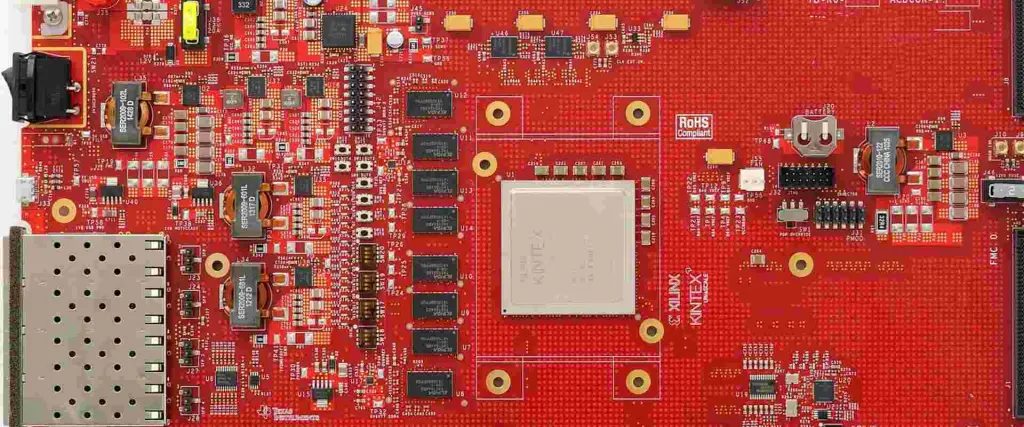
FPGA stands for Field Programmable Gate Array. FPGAs are semiconductor devices that contain programmable logic blocks and interconnects that can be configured to implement custom hardware functionality. Unlike Application Specific Integrated Circuits (ASICs), the functionality of an FPGA can be changed and reconfigured by the designer after manufacturing. This makes FPGAs flexible and versatile for creating specialized electronics and accelerating processing in a wide range of applications.
Some key capabilities of FPGAs include:
- Implementing digital circuits by interconnecting logic blocks
- Reconfigurable even after deployment in the field
- Supporting various interfacing standards and protocols
- Embedding custom processors and intellectual property blocks
- Prototyping designs before final ASIC fabrication
Leading vendors of FPGAs include Xilinx, Intel/Altera, Lattice Semiconductor, Microchip, and others. Designs are created using electronic design automation (EDA) software and a hardware description language like VHDL or Verilog.
Introducing the Xilinx Artix-7 FPGA
The Xilinx Artix-7 FPGA series provides a cost-optimized programmable logic solution for high-performance system integration. The family spans from low-cost, small form factor devices to large, highly capable FPGAs for the most demanding applications. All Artix-7 FPGAs are based on the unified 28 nm high-k metal gate (HKMG) process from TSMC.
Key features of Xilinx Artix-7 FPGAs:
- Built on 28 nm process with high density routing
- High performance DSP blocks, block RAMs, transceivers
- Low power optimization for power sensitive designs
- High bandwidth with up to 17 Gbps transceivers
- Leverages Vivado Design Suite for programming
- Wide range of packages from 15K logic cells up to 215K logic cells
The Artix-7 series delivers an optimal balance of performance, flexibility and reduced power consumption. The devices enable emerging applications in fields like communications, data centers, aerospace, and industrial automation.
XC7A200T FPGA Overview
The Xilinx XC7A200T specifically belongs to the Artix-7 200T variant. Here are some of its key features:
- 215,360 logic cells, each with a 6-input LUT and flip-flop pair
- 20,150 Kbits of fast block RAM
- 240 DSP slices with 25×18 multipliers
- Six clock management tiles, each with phase-locked loop (PLL)
- Eight receiver/transmitter blocks supporting up to 12.5 Gbps
- Two PCI Express blocks
- Two Ethernet MAC blocks
- Advanced configuration like AES and CRC encryption
- Multi-voltage, multi-standard I/O support
- 1.0V core voltage, offering optimized low power
With these capabilities, the XC7A200T provides a high performance, power optimized FPGA well-suited for applications like wireless, wireline, broadcast, industrial motors, automotive driver assistance, video analytics, and aerospace and defense systems.
Details of the XC7A200T-2FBG484I Variant
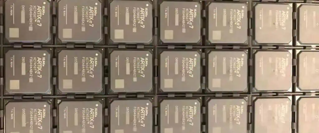
The XC7A200T-2FBG484I is a specific package variant of the Xilinx Artix-7 XC7A200T FPGA. It has the following detailed characteristics and configuration:
- 484 pin Flip-chip BGA (FBG) package
- 1.0V core voltage
- -2 speed grade, suitable for industrial temperature range
- Operating temperature range of -40°C to +100°C
- 27 x 27 mm package size
- 1.1 mm ball pitch
- 16 GT/s data transfer rate per differential I/O
- 17 x 17 mm silicon die size
- Pb-free RoHS 6 compliant part
This high-performance flip-chip package provides extensive I/O capabilities. The fine 1.1 mm ball pitch enables routing high pin count connections under the device. The industrial temperature range allows operation across a wide -40°C to +100°C ambient without degradation in performance.
FPGA Internal Architecture
Inside the XC7A200T FPGA, there are the following key functional elements:
Configurable Logic Blocks (CLBs)
- The basic logic cell with a pair of 6-input LUTs and flip-flops
- LUTs implement any 6-input logic function, flip-flops store data -215,360 CLBs in the XC7A200T FPGA
Block RAM (BRAM)
- Dedicated memory blocks of 36 Kb providing fast access
- Up to 20,150 Kb total BRAM in the XC7A200T
DSP Slices
- Specialized blocks with fast 25×18 bit multipliers and adders
- Allow high-performance digital signal processing
- 240 DSP slices in the XC7A200T
Clock Management Tiles (CMTs)
- Digital clock managers, jitter filters, frequency synthesizers
- Six CMTs in the XC7A200T, each with a phase-locked loop
High-Speed Serial Transceivers
- Eight serial transceiver blocks with up to 12.5Gbps data rates
- Support variety of protocols including PCIe, Ethernet, Aurora
Routing Matrix
- Interconnect matrix between logic blocks with various length lines
- Provides extensive routing flexibility between components
In addition to these elements, there are abundant I/O resources, PCIe blocks, configuration logic, and other components.
Key Applications and Uses
The XC7A200T Artix-7 FPGA can be deployed in diverse applications including:
- Wireless communication systems – 4G/LTE, 5G, Software Defined Radio
- Aerospace and defense – Radar, imaging, ruggedized systems
- Video broadcasting – Encoding, decoding, transcoding
- Medical imaging – Ultrasound, MRI, tomography
- Motor drives – Industrial, robotics, UAVs
- ADAS and sensors – Vision systems, lidar, radar
- Networking and telecom infrastructure
- PCI Express and Gigabit Ethernet platforms
- High speed data acquisition and analytics
- Hardware acceleration for AI edge inference
For these systems, the FPGA provides low latency, real-time signal processing and control capabilities not achievable with microprocessors alone.
Design Considerations

Some key considerations when designing with the XC7A200T FPGA include:
Power – Manage core, I/O and static power consumption especially in battery powered applications. Use power gating and low power design techniques.
Thermal – The FF484 package can dissipate up to 15W. Carefully model and monitor die temperature. Employ proper heat sinking.
Timing – Close timing margins impact performance. Optimize clock domains, I/O delays, and metastability.
Signal Integrity – Minimize noise through smart PCB layout and isolating analog/digital signals.
Radiation Hardening – Use mitigation techniques like TMR for aerospace and defense applications. The Artix-7 is not rad-tolerant by default.
Implementation Tools – Leverage Xilinx Vivado to fully optimize timing, resource usage, and power consumption.
Comparing to Other Xilinx FPGAs
Here is how the XC7A200T compares to some other devices in the Xilinx FPGA lineup:
| FPGA Series | Process | Logic Cells | Transceivers | DSP Slices | BRAM | Strengths |
|---|---|---|---|---|---|---|
| XC7A200T | 28nm | 215K | 8 at 12.5Gbps | 240 | 20Mb | Low cost, high capability |
| XC7Z045 | 28nm | 218K | 16 at 28.05Gbps | 900 | 27Mb | Higher performance |
| XC7V2000T | 28nm | 927K | 24 at 16.3Gbps | 2016 | 174Mb | Very high density |
| XCVU37P | 16nm | 893K | 16 at 32.75Gbps | 2520 | 145Mb | UltraScale performance |
| XCZU9EG | 7nm | 1.6M | 112 at 58Gbps | 5520 | 307Mb | Leading edge UltraScale+ |
The mid-range Artix-7 XC7A200T balances capabilities and cost-effectiveness. Other families scale higher or lower depending on application needs.
Conclusion and Summary
The Xilinx XC7A200T-2FBG484I is a high-performance Artix-7 series FPGA manufactured on a 28nm process. The device contains 215K logic cells and abundant DSP, memory, transceiver, PCIe, and networking resources. The flip-chip 484-pin BGA package provides extensive I/O in a compact footprint. With low power consumption across an industrial -40°C to +100°C temperature range, the XC7A200T FPGA enables advanced signal processing, control, and accelerated workloads in demanding environments and applications ranging from aerospace to 5G communications. Engineers can leverage the flexible programmable architecture and Vivado design tools to rapidly develop and iterate customized implementations.
Frequently Asked Questions
Q: What type of FPGA is the Xilinx XC7A200T?
A: The XC7A200T is part of the Artix-7 family, which is a low-cost, high-capability 28nm FPGA series from Xilinx.
Q: What is the difference between XC7A200T and other Artix-7 FPGAs?
A: The XC7A200T has the highest density and performance in the Artix-7 lineup, with 215K logic cells and features like PCIe, GigE MAC blocks and 12.5Gbps transceivers.
Q: What package is used on the XC7A200T-2FBG484I?
A: It uses a 484-pin flip-chip ball grid array (FBG484) package capable of very high I/O bandwidth.
Q: What design tools can program the XC7A200T FPGA?
A: Xilinx’s Vivado Design Suite is used for IP integration, synthesis, place-and-route, and configuration.
Q: What are some target applications of the XC7A200T FPGA?
A: Wireless communications, motor drives, video broadcasting, aerospace and defense systems, medical and industrial imaging, and network infrastructure.

