What is a Load Current in PCB Circuit?

heavy copper pcb circuit board

One of humanity’s most significant inventions, technology, has profoundly changed every facet of our existence. This fact is well supported by history. Our technical development has gone through a number of stages that have brought us to the level of comfort and ease we currently enjoy.

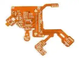
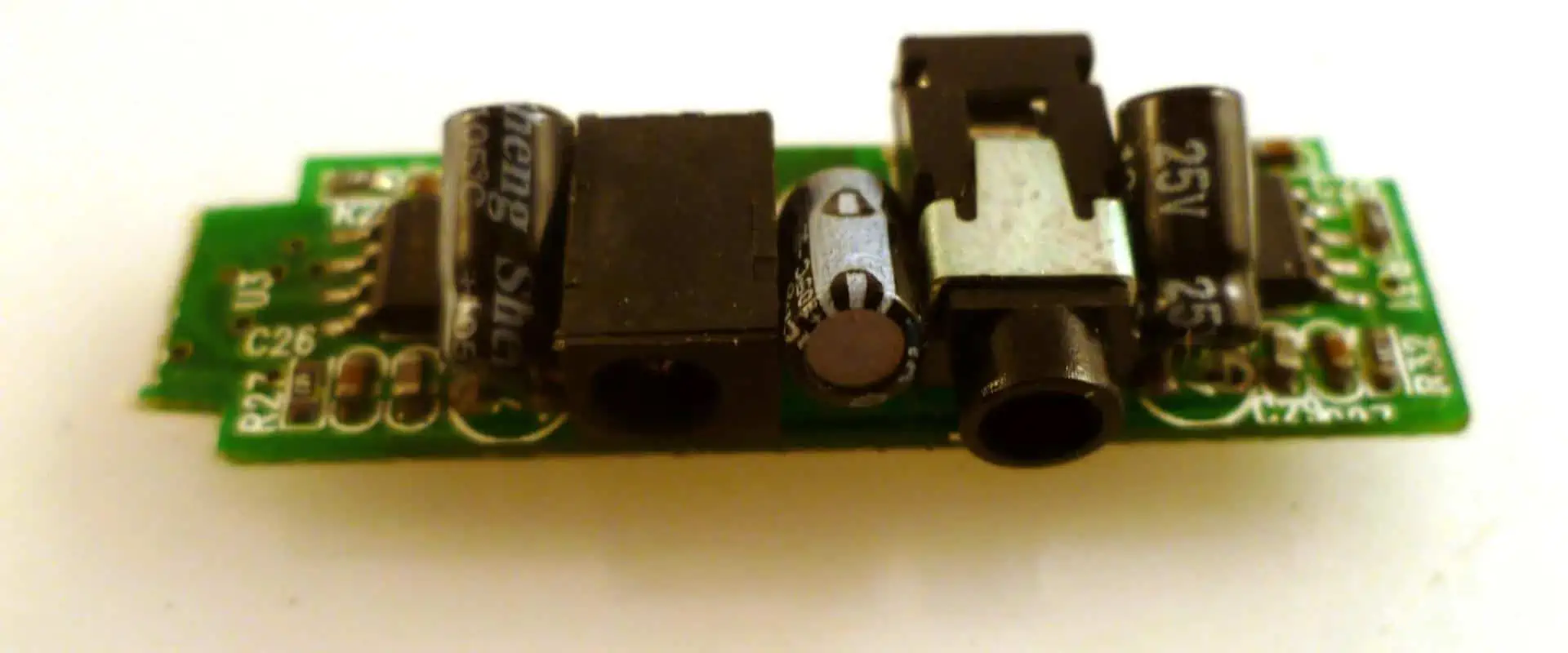
Going back in time, though, it’s plausible that this comfortable way of life wouldn’t have happened without printed circuit boards. In other words, our lives and the world we live in today would be significantly different without the load PCB. The load pcb has been essential to modern life in many spheres, from entertainment to the communications, from military to transportation, to education, health, and every aspect of our lives.

In addition to being the brains of every electrical device, these little boards also have an active history in all industries relying on technology.

What Does “Load Current” Mean?

heavy copper pcb

The quantity of an electrical current transferred from one power source onto the component or object receiving that power is known as the load current. Also, the majority of power supplies can only deliver a limited power even before they overheat and short out.

Therefore, this means that before an item is linked to a source of power, the requirements of the load of that item being used as well as the present load capabilities of the power supply should both be considered. If this load produced by this power supply exceeds the load that the connected item can carry, any connected device could sustain harm.

When this factor is ignored and a device is connected onto a power source that can handle a considerably higher load compared to what the device can handle, the device might overheat and sustain damage.

A source of energy is typically not immediately quantified in terms of the present load. Rather, power supplies were frequently described as voltage sources and measured regarding voltage. Whatever is attached to these voltage sources receives a steady current from them.

So far the quantity of the electrical current required from a power supply falls within the present load capacities of a power supply, current and voltage power systems function efficiently.

The short circuit often happens when a gadget that needs power has to draw more current out from a power source than that source can supply. This indicates that not enough current can be generated by the power source to successfully power the gadget.

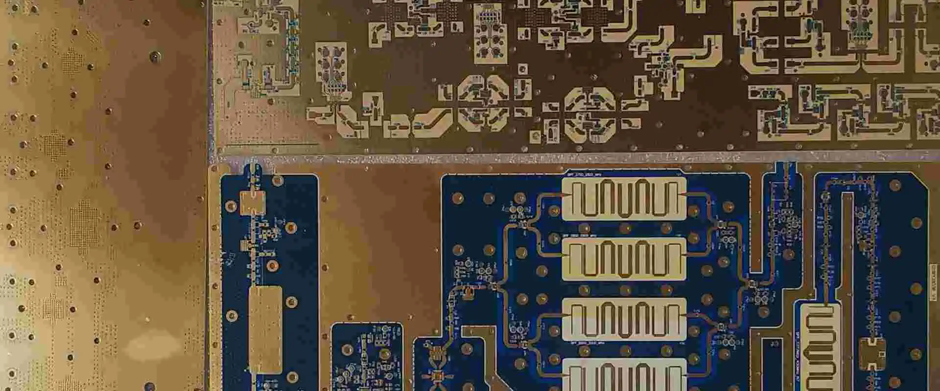
Using Active Load PCB Components

FULL PCB MANUFACTURING Quote

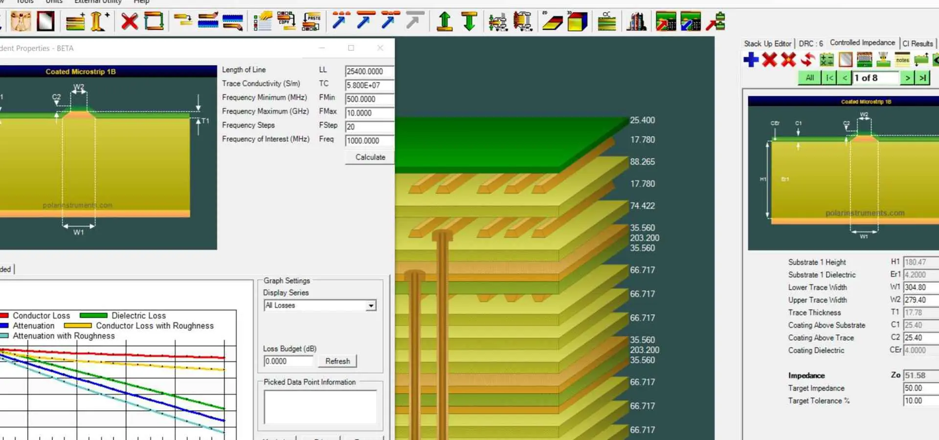
It is necessary to simulate load pcb components that are active using a tested model because they will provide further interesting behavior. For usage with PSpice as well as other simulation applications, many load pcb component makers have fortunately taken the trouble to provide certified simulation models. This saves a lot of time and uncertainty when analyzing how various load pcb components affects the input waveform as well as their electrical behavior.

You require a collection of simulation tools that can demonstrate how the current loads impact signals within that frequency domain as well as time domain when you wish to mimic signal behavior inside a complex circuit. Your PCB analysis and design software’s pre-layout simulation tools will have access to the most advanced simulator. The robust PSpice Simulator integrates with front-end design tools from Cadence in creating a comprehensive system for generating schematics and analyzing how the current loads impact signals.

Load Current: How Does it Work?

The quantity of an electrical current transmitted from a particular source of power to the appliance or equipment receiving that power is referred to as the load. The majority of power sources can only deliver a limited amount of power until they short out or overheat.

This means that before an item is connected onto a specific power source, the requirements of the load requirement of that item utilized as well as the capabilities of the current load of a specific power source must both be looked into. If this load produced by the source of power exceeds the load the connected item can handle, any connected item could sustain harm.

When this factor is ignored and a device is connected into a source of power that has a considerably higher current load compared to the device can handle, the device may overheat as well as sustain damage.

The energy source is typically not immediately quantified in terms of the present load. Instead, sources of energy are frequently described as sources of voltage and are frequently quantified when it comes to voltage. Whatever is connected to these voltage sources receives a steady current from them.

So far the quantity of the electrical current needed from that power source can be seen within the power source’s current load capacities, current and voltage power systems function well.

The short circuit often happens when a gadget that needs power has to draw more current out from the source of power than just the source can supply. This indicates that not enough current can be generated by the power supply to successfully power the gadget.

How does the PCB Circuit’s Load Current work?

It is typically clear how various circuits as well as loads affect different signal behaviors at the output of the circuit when using basic circuits as well as simple sources of signal. It is occasionally clear how this circuit itself affects signals or how the current loads influence signal behavior when dealing with more sophisticated circuits as well as wideband signals.

Although you could calculate these features of a signal behavior manually, not everyone can be a mathematician, therefore you’ll need to use different tools in speeding up complex circuits analysis.

You could quickly assess how the load impedance impacts signal behavior present in a frequency domain compared to the time domain when you are having access to any strong simulation engine present in the schematic design during the stage of PCB design. You may see how a specific load as well as its load pcb affects a signal using several straightforward simulations.

What are the Differences Between the Load Current as well as the No-Load Current Supply?

An essential factor to take into account is the industrial sensor’s current consumption. You can choose the appropriate supply of power for that application and size wire suitably by knowing how much current each of your devices present on the machine consumes.

On the data sheet, there are just two specifications that merit attention, which is the no-load as well as the load current.

The No-Load Current Supply

This is probably the most crucial specification to consider when sizing the power supply. The current used by a device when it is not in use is known as the no-load current supply. Whether or not a load is connected onto the output, the current is still used.

The maximum current consumption across all voltage as well as temperature ranges is this.

Load Current

For this it is the biggest misunderstanding around this specification. The user can simply find out the amount of current that our industrial sensor will be able to deliver to an actual load by looking at load current. It’s not how much current a sensor would deliver onto a load.

To properly size the supply of power, you must first know what load is attached onto the sensor. 95% of the sensors in use today are wired to I/O cards with really low current. Depending just on hardware architecture, the I/O card will use between 3 mA to 9 mA and at 24 VDC for its load current.

Only if the sensor gets switched on and then the output is active does this current get used and consumed. It goes without saying that you should always assume that all sensors remain on at all times when sizing the power supply. You should always prepare for the worst-case situation, and your system should include a unique safety margin.

What are Electronic Circuits?

copper core pcb
copper core pcb

Every circuit consists of three components. There is one source of power, and two cables come from such a source. Follow those wires until you reach the resistive load; circuits often power resistive loads like motors and lights. Each circuit is primarily composed of conductorsโ€”wire when we talk of copper, as well as plastic and copper when we talk of a Printed Circuit Board, a load, as well as a switch. Furthermore, a switch is also present in the power circuit.

The continuity principle is the fundamental rule of electricity. If only one wire exists, electricity will pick the least resistance path; if there are multiple wires, electricity will choose the other path. This indicates that electricity travels along the entire wire before discharging at the opposite end.

The electricity laws play a crucial role when there are multiple paths for electricity to travel through in very complicated circuits. Any circuit can have its electrical flow limited so that just a certain amount can be transferred.

Conclusion

If that load being supplied by the source of power is larger than the load of any connected item that it can handle, damage may result. This is why load pcb is very necessary.

What are the Benefits and Design Considerations of the HDI Multilayer PCB?

multilayer pcb stackup

Today’s world has gradually experienced a huge leap thanks to HDI multilayer PCB. HDI multilayer PCB has been impacting the entire technical industry over the last few years. Compared to typical multilayer boards, the HDI multilayer boards come unique. Additionally, compared to ordinary PCBs, the HDI multilayer PCB include more interconnections.

A board having HDI has 120 to 160 pins per square inch of surface area. There are various layers of this board. The primary subject of this essay is HDI multilayer PCB.

What Does HDI Multilayer PCB Mean?

A multilayer pcb with many interconnections is called the HDI multilayer PCB. The components on this board are positioned next to one another to give it a compact appearance to the circuit board.

This board is used by various technological sectors, including the automobile and military. The HDI multilayer PCB alters the board’s overall performance and improves signal integrity.

Specially created HDI circuit boards offer a higher degree of performance as well as processing capacity inside a smaller area. Developing this board was driven forward by the desire for more potent and compact devices from sectors like telecoms.  Other significant elements, however, also had a significant role in developing the HDI multilayer PCB. The developments in IC technology are included in these factors.

These trends forced PCB makers to reevaluate the layouts and interconnect design of their boards. Additionally, HDI multilayer PCB can pack more power into a smaller space. This board’s capacity to carry out this task is based on integrating new techniques for the interconnect like the vias in the microvias and pad.

What are the Benefits of Using the HDI Multilayer PCB?

nanya-pcb-material

The HDI multilayer PCB provides different benefits when utilized in different applications. Let us consider some of them.

High reliability

The HDI multilayer PCB is far more dependable than a typical multilayer board. This PCB’s integration of heaped vias gives the PCBs optimal robustness and resistance. Therefore, once you decide to invest in this board, you don’t need to bother about its performance.

Reduces extra charges

You will receive a lot of value for your investment in this HDI circuit board. This HDI multilayer circuit board ensures sufficient quality and performance without charging extra. A single PCB that does everything is this. As a result, when you have the HDI board, you no longer require multiple regular circuit boards for various purposes.

Improvement in electrical performance

The spacing between components is less and there are more transistors on HDI PCBs. This could aid in enhancing electrical performance. These features also make minimal consumption possible, this helps in enhancing the signal integrity later on.

Smaller size and lighter weight

On the two sides of the board, extra components can be fixed. Additionally, this board allows for increased functionality while lowering its size and weight.

HDI Multilayer PCB Design Considerations

FULL PCB MANUFACTURING Quote

The HDI multilayer PCB is produced using different methods than a multilayer conventional PCB. Additionally, HDI multilayer circuit board manufacture starts with its design. As a result of the necessity of taking certain thermal, physical, and electromagnetic elements into account, this design process for the HDI multilayer PCB comes quite complicated. When planning your manufacturing, keep a few design factors in mind.

Types of Via Fill

The types of via fill will be determined by the particular application as well as PCB specifications. Use matching via fill types that suits your application at all times.

Additionally, there are various forms of via fill, including non-conductive epoxy, conductive epoxy, as well as electrochemical plating. The most popular via fill is non-conductive epoxy.

Sequential lamination

The Circuit board designer presses and heats copper to mix it with PCB cores during lamination. The quantity of heat and pressure required also depends on the board’s layers. The Circuit board designer must drill vias after the laminating phase is finished. HDI multilayer boards frequently have their vias drilled. Sequential lamination additionally avoids shifting and breakage during drilling.

Technology for laser drilling

Laser microvias are commonly needed in multilayer HDI PCB designs. Typically, laser drills are used to generate these microvias. Furthermore, these drills frequently produce around 20 microns of laser with respect to the diameter. Also, this laser has the ability to cut into metal as well as glass and this is why it usually creates holes that are extremely tiny

Impedance Control

To ensure that impedance will not really compromise signal integrity, designers of HDI multilayer PCB must keep trace width as well as dielectric layer thickness tolerances around +- 10%.

What are the Applications of the HDI Multilayer PCB?

HDI PCB Board Laminate Structure-2

HDI technology is essential to the majority of cutting-edge technologies. Additionally, manufacturers have been able to create smaller gadgets without sacrificing performance or durability thanks to the shrinking of electrical components. The HDI multilayer PCB is perfect for usage in a variety of applications, including:

Communications

Broadly speaking, equipment that makes it possible for communication devices and gadgets to work uses the HDI multilayer PCB. These boards come in switches, modules, semiconductors, and routers. Additionally, the HDI multilayer PCB is frequently used in digital video and audio equipment. Many personal devices for communication use these boards.

Medical equipment

For usage in cutting-edge electronics medical devices such monitoring, imaging, as well as laboratory analysis instruments, HDI PCBs are appropriate. When included in gadgets, these boards enhance their performance. Additionally, the precision of the medical testing as well as monitoring is increased with HDI multilayer PCB.

Aerospace and the automotive

Electronic producers may cram more capabilities into tiny places and gadgets thanks to HDI boards. Smaller space and lower weight are important in the aircraft and automobile industries. As a result, HDI multilayer PCBs are much favoured in different industries over regular multilayer boards. More computers and connections are used in modern vehicles.

These days’ automobiles contain a number of microprocessors. These microprocessors become essential for control, diagnostic, and safety features. Additionally, HDI multilayer PCB is necessary for various functions including rearview cameras, WiFi, as well as GPS.

Industrial Uses

Industrial machinery is much more computerized compared onto the way to the ever today. IoT devices are also frequently used in manufacturing, warehousing, and other industrial contexts. The majority of cutting-edge industrial machinery includes HDI technology. Additionally, machines are also incorporating smart sensors to gather utilization information.

Which Three Techniques Do Manufacturers Employ When Assembling HDI PCB Stackup?

HDI PCB Board Laminate Structure-Blind and Buried vias-3

Manufacturers can assemble HDI Circuit board stack-up in three different ways. Let us consider checking out what they offer ย 

Sequential Lamination

This is the process of sandwiching a sub-composite laminated and the dielectric between the two layers of copper. For sequential lamination, manufacturers employ buried vias, blind vias, as well as plated through vias.

Standard Lamination

Regular lamination entails producing HDI material in successive layers. The manufacturer then binds the layers together. Lamination is a technique used to stop copper from unintentionally transmitting signals. For this method, plated through-hole predominates.

Lamination buildup using micro vias

Even if micro vias are being used, the lamination process is still being done.

Features of the HDI Multilayer PCB Stackup

HDI Multilayer PCB has some special attributes. These include  Very small vias are among them. The industry refers to them as micro vias. Manufacturers use a laser to drill its micro vias, which have a 1:1 aspect ratio.

Another characteristic of HDI Multilayer PCB stack-up is buried vias. The stack up’s inner layers are joined together via its buried vias.

There are also blind vias inside this mix. They link the outer and interior layers. The connection is made using blind vias without taking up the full board. Elic, which are copper-filled, stacked micro vias that connect the PCB’s different layers, are present.

How Can I Tell If a Material Is Appropriate For Manufacturing HDI Multilayer PCB Stackup?

shengyi-s1141-laminate-PCB

The entire HDI multilayer PCB process is at risk if the wrong PCB material is used. In order to obtain the right materials to suit the job, manufacturers need provide answers to some fundamental inquiries.

  • Does the material have what is needed thermally? If so, it is appropriate for the whole process.
  • Is the substrate material compatible with the dielectric? Any dielectric you choose has to be suitable with the substrate material used for the core.
  • Are micro vias very reliable?
  • This is the material’s ability to withstand thermal shock
  • Does the plated copper adhere well to the dielectric?

What Challenges Are Faced During HDI PCB Stackup?

The difficulties with the HDI Multilayer PCB stack-up are as follows.

  • Vias have a tendency to be delicate. This is due to the fact that while these may be susceptible to significant thermal stress, they are crucial materials for HDI multilayer PCB stack-up.
  • Manufacturers cannot avoid using the right materials. No room exists for material management or improvisations.
  • Plating issues Aspect ratios must be followed by manufacturers to ensure plating integrity.
  • The HDI Multilayer PCB equipment is fairly pricey.
  • When businesses utilize pre-pregs, the pre-pregs’ glasses frequently shift the laser’s direction.
  • The shift in direction causes the via holes of the laser to have poor quality with respect to its shape.

Conclusion

Many contemporary electronic devices have been developed with the help of the HDI multilayer PCB. It is more likely that HDI technology will be incorporated as electronic gadgets become smaller and more portable.

Importance of a Probe Card PCB in Semiconductor Wafer Test System

Probe card pcb

In general, probe cards can be seen as expendable and maintenance is required to guarantee their performance and effectiveness. The resistance may rise and obstruct accurate readings owing to overload and the buildup of debris out from the wafer’s binding substance on the probe’s tips or probe needles.

What Does a Probe Card Mean?

In essence, probe card can be described as a board or interface useful in performing wafer testing on the semiconductor wafer. Before being produced and transported, integrated circuits on the wafer are tested for electrical characteristics and performance via this connection to the Automatic Test Equipment.

In essence, probe card acts as a platform which enables mechanical and electrical contact between both the electronic test system and the device undergoing testing. Each Probe Card has these components:

  • The Printed circuit board
  • The Organic Substrate (Multilayer)

We also see that this Probe Card forms a component of a wafer test system up to this point, but it must be tested before being incorporated into the test system. It is required to fulfill the standard for high – performing power as well as signal transmission during electrical testing due to the device bandwidth as well as increasing power demands. The difficulties for such probe card testing are driven by these needs.

In order to match all the pads present on that device being tested with the probes, the probe cards were created. The user must provide the manufacturer of the probe card PCBs with the device layout’s mechanical drawings or the device’s sample in order to have a probe card made.

For simultaneous multi-site and integrated circuit testing requirements, probe cards could be simple only with one probe (a diode), or they can be sophisticated possibly reaching a thousand probes. Edge finger (maximum to 48 pins) as well as ribbon cable is typically utilized for the cable connection into that probe card (which can reach 160 pins).

How Does Probe Card Function?

Probe card Circuit Board

Take the production of semiconductors as an example to see how to simplify the process. There are various integrated circuits located during silicon manufacturing.

After, this wafer gets chopped, packaged, and then shipped. However, the functionality of the circuits must be verified before packaging is done. The probe card is used to help with the electrical test. To establish the electrical path in between the tester and the semiconductor wafer, this probe card is installed into a prober which is then connected onto the tester. This probe card subsequently connects with the IC chips’ pads on the wafer using its metallic needles or elements to transmit the electrical data and necessary test parameters.

Since the tester’s head must be attached to the pads or metal bumps present on that wafer so as to communicate that electrical data, the prober could be thought of as such. This prober is utilized in docking the probe card, lower it to the wafer, and then wait for the bumps or needles to connect before establishing the current flow between the connections. Scrubbing off the layer of oxide and connecting to the surface of the metal beneath requires movement of these probing needles when they establish contact with those metal bumps present on the wafer.

Advanced Probes Types

FULL PCB MANUFACTURING Quote

The range of probe cards available today when choosing the type of card to employ to test the wafers is evidence that probe technology has advanced significantly in recent years. Let’s examine the several categories of sophisticated probes:

Vertical Probe

These vertical probes are cards which are utilized to evaluate multi-die devices like those related to general-purpose microcomputers and logic. It is the perfect option for high frequency and small pad wafers since these needles come typically brief and placed vertically with relation to a substrate.

MEMS-SP

This kind of probe makes use of the benefits of the MEMS technology as well as enables very accurate and dependable testing of microprocessors and logic devices using this probe card. The most cutting-edge probe technology now on the market is known as MEMS, or Micro Electro Mechanical System. With just one touchdown, it has the ability to establish one connection onto the wafer.

U-Probe

Probe cards called the U-Probe can be described as the most effective when measuring memory devices. It can make contact with the wafer which is about 12 inches long with just one touch downwards or contact. It may be utilized anywhere, in whatsoever position on that semiconductor wafer, and produces another even scrub in order to produce the finest results.

Reasons Why the Probe Card PCB is Used

Probe card Board

Below are the common reasons why probe card PCBs are used. These include manipulator limits, layout of the device, as well as production. Now, letโ€™s consider each of them in detail.

Manipulator Limits

A standard prober could only position 8 to 12 manual manipulators all around a platen opening without the need for the probe card. Additionally, each probe tip must be manually adjusted by the operator, which is a laborious process that takes a lot of practice and time.

Layout of the Device

Whenever the user needs to probe any device that has a high pin count (>12), the probe cards play an important role.

Production

Probing applications for production make heavy use of probe cards. Production applications could be as simple as a diode with one probe or as complex as integrated circuits with hundreds of probes.

Conclusion

This probe card can be electrically attached to the test instrument and docked mechanically to the prober. The main goal is to create an electrical connection between both the test equipment and the wafer’s circuits, allowing for validation as well as testing of these circuits prior to dicing and packaging. It is made up of a circuit board as well as different contact elements, which are typically made of metal but could also be made of other materials.

To assist reduce manufacturing costs and boost productivity, we design and produce a wide variety of probe cards with high performance.

Capabilities and Benefits of MLO PCB

Rogers PCB

The MLO has been integrated in several applications because of its characteristics. The capabilities of MLO have helped the development of a number of products. Also, the MLO technology features great properties like fine line high density, high current handling, interconnect technology, tight tolerance control and low profile copper. In this article, we will provide more details about the MLO technology and how it is impacting several areas, especially PCB manufacturing.

What is Multilayer Organic (MLO) Technology?

Multilayer Organic is a technology that integrates extreme low loss organic materials. This enables a high stability and high Q over frequency.  Also, the MLO technology features great properties like fine line high density, high current handling, interconnect technology, tight tolerance control and low profile copper.  Due to these properties, this technology helps in the production of Diplexers, Filters, Capacitors, conductors, Capacitors, Crossovers, Diplexers, and Couplers for RF & Microwave applications.

Product designers have to integrate the common components in RF systems to take advantage of the capabilities of the embedded device. These components include couplers, networks, diplexers, and filters. Designers can also implement these components in various circuit topologies. However, these components need to be transformed in lumped element structures. Designers need to design these structures to offer the desired level of performance since very high component densities are needed in small form-factor packages.

The multilayer organic packaging was specially developed to implement RF System on Package (SoP). This packaging process helps vehicle manufacturers to embed most of the crucial RF passive components in a substrate under the RFIC while still ensuring high performance. Multilayer organic (MLO) is a crucial innovation in design and process.

Advantages of MLO Technology

Taconic RF-60TC PCB

The MLO technology has a lot of advantages. This makes it ideal for use in a wide range of application. The advantages of MLO technology include:

  • It has a multilayer structure which enables high order filters
  • Features tight tolerance and high precision
  • Does not require tuning
  • Has lower profile components
  • Lot to lot and part to part repeatability
  • It doesnโ€™t perform differently in response to changes in temperature
  • Can mount discrete components on custom MLO devices to enhance performance
  • The expansion level matches with that of printed circuit boards
  • It adheres to the ASTM E595
  • It has fine line density

Applications of MLO Technology

There are several applications of MLO technology.

  • GPS
  • Mobile communications
  • Wireless LANs and Aps
  • Satellite Applications
  • RF Power Amplifiers
  • Low Noise Amplifiers
  • Instrumentation
  • Military and Commercial Radar
  • Optical Drivers
  • Vehicle Location Systems
  • Filter Networks
  • Medical Imaging Electronics

What are the Capabilities of MLO Packaging?

FULL PCB MANUFACTURING Quote

Integrated Circuit (IC) packaging is crucial in reducing the size of wireless products. Also, the importance of IC packaging is evident in electronics. In as much as Moore’s law contributes to the increasing density of digital silicon components with every new process node, RF components integrated in modern broadband wireless products donโ€™t apply the Mooreโ€™s law.

Furthermore, multi-band RF products are not yet acceptable in a wide range of applications. Therefore RF front ends comprise heterogenous RFIC technologies with passive components. Also, RF modules are now the standard form of packaging microwave components for wireless applications. The SMT based designs is facing some challenges. These challenges include the rapid increase in the production of wireless-capable products, the proliferating frequency bands, and the complexity of wireless technologies like OFDM.

These challenges alongside some form factors have made the RF design task to go back into the radiofrequency semiconductor supply chain. Also, the integration of high performance passive components and RF ICs, an SoP approach to RF design will result in a new generation of RF modules with cost savings over SMT assembly. Patented multilayer organic technology

The multilayer organic packaging was specially developed to implement RF System on Package (SoP). This packaging process helps vehicle manufacturers to embed most of the crucial RF passive components in a substrate under the RFIC while still ensuring high performance. Multilayer organic (MLO) is a crucial innovation in design and process.

The MLO Stackup

An MLO substrate has RF dielectric layer(s) in between layers of laminate to offer bonding, routing, and shielding for placement of RFIC die and SMT. The dielectric layer must have a high Dk and low loss at the wireless frequency ranges. This offers high capacitance density. However, these properties could be counteracting for some materials since you can achieve a high dielectric constant when polymers are being filled with dielectric materials.

Therefore, thin dielectric layers are important. These days, copper clad films now have low-loss formulations of PTFE and LCP. LCP (liquid crystalline polymer) has a low dielectric constant. This property is favorable for various RFD and high speed application. In PTFE case, you need advanced filler materials to enhance dielectric constant.

Standard lamination processes can help to achieve high performance RF packages if you carefully select bond ply materials and other laminates. You can etch and assemble the layers of the stackup if you have completed module design. MLO technology is integrated in the printed circuit board manufacturing process.

Process Control in MLO

HDI PCB Board Laminate Structure-2

The capability to regulate process parameters and to forecast their effect on device yield is one of the requirements for enabling MLO based products to be produced in large volume. There are crucial parameters for regulating the tolerances of embedded component. Inductors, tools, and hole These parameters include line width and spacing, core layer thickness, and layer to layer registration.

It is very complex to derive these parameters as it involves tradeoffs between RF design parameters and fabricator capabilities. Process tolerant component designs were developed since there will be higher cost if tighter control is integrated over these crucial parameters. Design for manufacturability (DFM) is a crucial element for the development of patented multilayer organic technology.

Conclusion

There are several areas where MLO can be integrated for a wider range of applications. The MLO design process seeks to power output and optimize gain within a particular process constraint. Also, MLO enables designers to achieve any capacitance or inductance value and as well offers more degrees of freedom when wide-band microwave circuits are designed. The characteristics of MLO have helped in improving the impedance of a PCB.

What Function Does the Copper Layer PCB Serve?

Aluminum PCB VS. Copper Base PCB

Once the etching is finished, copper layers can be considered as a circuit board with copper on it. Typically, this consists of tracks and pads or power and ground layers.

We’ll talk about the uses of a copper layer PCB in this post. We will also go over how to create output files suitable for the copper layers, among other things.

Why Do Printed Circuit Boards Use Copper?

When it comes to PCB design, two terms become crucial.

These consist of copper balancing and copper thieving. Despite the fact that they are frequently used interchangeably, in this post, we shall highlight the key differences between the two.

Copper Balancing

copper layer PCB

The combination of the copper areas and non-conductive patterns into the circuit board is known as copper balancing. This prevents the board from potentially bending while manufacturing is taking place. Additionally, asymmetrically constructed PCB layer stackup might cause the board to warp during fabrication.

Additionally, because of excessive heat used for soldering, any uneven copper included in the board’s structure may twist during assembly. Your PCB CAD’s design system will assist in adding area fills as well as pours to the sparse sections of your board to help the copper in balancing your design to combat this.

Copper thieving

Introducing non-conductive patterns of copper to the circuit board is known as copper thieving. But in situations like this, the only options are to thieve as well as discharge some of the electrical current used for the board plating.

Additionally, the current applied into the board in order to facilitate plating can become more concentrated and targeted towards the characteristics on its board regions that contain isolated as well as lonely traces.

The scenario may result in the trace being under-etched, producing a “mushroom”-like profile instead of the expected clean and squared edges. The cross-section of this trace can show significant undercutting, and the right-side trace is then squared off as you would like.

Choosing the Best Copper Material for Copper Layer PCB

Copper-Clad-Board-Material

Copper Foil

The cathode component of your electrolytic material can be called the copper foil. On the base of the circuit board, this substance is placed onto the continuous, as well as thin layer of metal foil. Additionally, it is simple to attach onto the insulating layer, accepting the protective layer, coupled with a corroded nature so as to form the pattern of your circuit.

Prepreg

Prepreg is an abbreviation for pre-impregnated. Also, t his is referred to as resin-impregnated fiberglass. Although the resin is usually pre-dried, it has not yet been solidified. As a result, when heated, this adheres, flows, and becomes completely submerged. In order to strengthen the prepregs, fiberglass is added via a specific adhesive layer, similar to FR4 material. Prepreg names are all derived from the type of fiberglass utilized.

Standard Thickness of Copper Layer PCB

The most commonly used units for determining copper layer PCB thickness in circuit boards.

However, the majority of individuals are unaware of the type of thickness it has. Undoubtedly, not everyone thinks in mils before converting to their favorite measurement system utilizing the conversion tool of choice.

Additionally, the bulk of Circuit boards are typically built with a copper layer that is 1 ounce thick. Whenever the customer fails to provide particular specifications for PCB production, the manufacturer often assumes the standard 1 oz when quoting and creating the design. Additionally, it is wise to increase its copper’s thickness and the width of the traces if that customer suddenly decides their design requires more current compared to the standard 1 ounce can carry.

Yes, the price will increase if the copper is thicker. However, there really are times when this is absolutely required. Additionally, the price increase is not solely due to the higher cost of the raw materials, but also to the longer processing times required for heavier weights of copper. In addition, handling and performing it could be a little bit trickier.

Processing the Copper Layer PCB Thickness

FULL PCB MANUFACTURING Quote

Etching is used to create the copper traces on the board. The interior layers and the surface are both the same in this regard. Etching is a crucial process in the production of PCBs. This laminate sheet, that is completely covered in copper, is the first layer to be constructed. Etching is the process of removing extra copper using an ammonia-based solution from traces and other locations, such as component pads and annular rings to serve the vias.

This copper thickness is usually where the sheets begin. To meet the required specifications, this thickness can be increased, etched down, decreased, or plated up. Due to the manufacturing technique used to create these sheets, the surface has a certain type of roughness that aid the bonding onto a dielectric material.

Additionally, this can have a detrimental impact on its signal integrity and at a greater frequency.

Additionally, for frequencies higher than 100 MHz, there is a skin effect that causes current to flow more frequently at the interior surface of the trace than through the middle part of this conductor. This causes the effective resistance of the trace to increase as well as oppose current flow.

How to Create Output Files for the Copper Layer PCB

Use “flashes” for this pads whenever you create data files. This prevents “painted/drawn” pads from being used. Additionally, avoid “painting” or using little draws to fill in the bigger copper planes and sections. Use contours or polygons to create areas or planes whenever possible.

Gerber X2 output as well as other formats includes these as standard features. Additionally, be sure to include your board layout each time you are outputting that copper layer of a PCB. This makes it easier to spot any errors with rotation, mirroring, as well as data alignment.

The easiest way to do this is to utilize a certain narrow line, the center of which is the outline of the board.

Conclusion

We believe we have adequately outlined the purpose of a copper layer PCB. Should you have some questions, please contact us at any time.

What are Sculptured Flex Circuits?

Flexible Printed Circuit Board Manufacturers

The Sculptured Flex technology modifies the standard flexible circuit technology by substituting the male connector pins for copper traces that are unsupported that extend beyond the board’s edge. These copper traces have varying thicknesses; the connector parts are thicker and more durable, while the remaining portions of this circuit are thin enough just to allow for flexing and bending. Due to its ability to increase space efficiency while reducing PCB width by doing away with connectors, sculpted flex is becoming more and more popular.

In order to assemble a connector on conventional flex circuit boards, the board must feature PTH appropriate for receiving the connector pins as well as the solderable pads that works great for the pitch matching of the surface mount ZIF socket.

Once this connector gets soldered to the PCB, additional support is required to relieve stress at the board’s junction as well as the connector. However, all of the above can be avoided with sculptured flex circuits.

Sculptured flex circuits begin with 7 oz. of thick copper. This creates the traces of copper that will stick out from the circuit board so as to produce the connector’s pins. Following the removal of the undesirable copper, more careful etching decreases the remaining traces to a thickness that support high flexibility, while plating using metals like tin, gold, and copper increases the traces’ thickness present at the different edges. While maintaining the majority of this circuit, the selective sculpturing results in thicker traces occurring at its edges.

flex-circuit-manufacturer

Its base dielectric must then be removed from beneath its thicker traces utilizing back-baring technology. Fabricators choose to pre-punch or drill its base dielectric so as to reveal the traces which will later become connector pins rather than ablate or remove the dielectric with lasers.

When Should You Use This?

  • Integrated design lowers labor expenses for assembly (savings for the customers)
  • Getting rid of connecting parts reduces weight and improves flexibility.
  • Offers exceptionally high performance and dependability
  • Whenever there are design constraints on space, this is used

Features

  • A crucial component of this conductor designs are fingers.
  • Tailored to fit any mating board pitch as well as configuration
  • Available formed or straight contacts
  • Traces of unsupported termination
  • Because it is thicker, the terminal point can be used as the connector right away.
  • Removes any mechanical connection points, as well as ensure more reliable connection.

Advantages of Sculptured Flex Circuits

Sculptured flex circuits are excellent for plugging in straight in sockets of female connectors or attaching directly to Circuit boards using a quick insertion procedure to interface with connectors delivering solder cup termination. They are therefore appropriate for space-constrained, tough applications. By not requiring mating or wire stripping connectors, it also saves money.

A conventional product having contact-area configurations present on the opposite or same side is possible with the sculptured flex circuits, enabling the mirroring of signal layouts in-between two Circuit boards.

They inherit the advantages of flex circuits, including greater signal integrity as well as strong resilience to damages from vibration and bending, because sculptured flex is essentially a flexible circuit. For different differential signals, of low voltage, as electrical connectors present in-between display boards as well as Circuit boards, and in place of cable jumper assembly in high-vibration applications, sculptured flex circuits can therefore be a common product that is readily accessible off-the-shelf.

HD televisions and large display applications are also excellent candidates for sculpted flex, particularly when it comes to simplifying cable jumper assembly. Additionally, by using FPC connectors with an extremely low pitch, manufacturers may easily achieve tight tolerances required for dependable connections.

A common use for sculptured flex circuits is in jumpers, sometimes known as the sculptured jumpers, which offer a straightforward but affordable method of connecting rigid circuit board with the panel-mounted components. Users can attach the unsupported and exposed fingers of the sculptured jumpers directly to SMD pads or thread them via PTH directly on the SMD pads.

In conclusion, sculptured flex circuits does have a variety of advantages, including:

  • removing the requirement for the ZIF connectors
  • lowering the cost of assembly labor
  • expanding adaptability
  • Increasing performance and dependability

Considerations in Sculptured Flex Circuits Design

FULL PCB MANUFACTURING Quote

The industry classifies Sculptured Flex Circuits as a subset of Differential Copper Circuit boards. These Bump Plated Circuit boards are another type included in this group. Although bump plated Circuit boards have extensively plated surface mount pads present at its ends, sculptured flex Circuits have uncovered metal fingers that allow bare metal interconnections similar to plug-in connectors. Often, these plated surface mount pads have a plating layer that is thicker than 5 mils.

Top-quality sculptured flex circuits made of beryllium copper, stainless steel, or aluminum could be produced by manufacturers for use in commercial applications. When developing sculptured flex circuits, polyimide is regarded as the most frequently used material for its dielectric; however, the choice also varies depending on the thermal and mechanical requirements of the application. Fabricators can still use PEN or polyester as the dielectric where necessary.

The application mostly determines the hardness and thickness of finger conductors as well as the type of copper to use for the sculptured flex circuits. Although no specific restrictions are available when creating artworks to serve sculptured flex circuits, the fabricator must be adequately informed of the copper and dielectric requirements.

Summary

Single-sided or double-sided flex circuits without or with PTH make up the majority of the sculptured flex circuits. Also, they are sculptured thick pins that resemble terminals and continue these copper traces present on its flex, but go beyond the limit of the main dielectric material.

Because they can be soldered directly onto SMT pads, PTHs, or plugged into the female connectors, sculptured flex circuits offers an infinite number of contact configuration options. This eliminates the requirement for connectors, reduces the cost involved in assembly and of the materials needed, and increases the system’s dependability and performance.

Why FR4 PCB Assembly is Suitable for Some PCB Applications

PCBA electronics

The majority of electrical engineers, as well as those working with circuit boards, know much about FR4. The majority of rigid boards are constructed with FR4 as their base material. Many people don’t even know what FR4 is, let alone know why it’s the most often used PCB base.

After constructing the Circuit board, your task is far from finished. The board still needs to be put together by attaching electronic parts to it. When you’ve finished, your PCBA is complete. Continue reading to find out more regarding FR4 PCB assembly, including what exactly they are, why they have become so popular, as well as how their characteristics stack up against those of other options available in the market.

What Does FR4 Substrate Material Offer?

FR4 is a name as well as a standard rating, and it can also be written simply as FR-4. This name is used to describe the epoxy-laminated sheets with fiberglass reinforcement that are utilized in the production of printed circuit boards.

This name also serves as a specific grade for the sheets made of epoxy laminate, though. The grade, which is generally considered to indicate the basic quality of the laminate sheet, applies to a wide range of designs and sheet materials. Flame retardant is indicated by the “FR” present in its name, while the “4” distinguishes this material from the others in its class.

The substance widely termed FR4 is made of composite materials. Fiberglass that has been woven to a cloth-like, thin sheet forms the material’s base layer. FR4 receives the essential structural stability from the fiberglass.

A flame-resistant resin is then used to encircle and bind the inner fiberglass layer. Along with the other physical characteristics, the resin is whatever gives stiffness to the material.

Electrical designers and engineers adore FR4 sheets like a base material for PCBs. This popularity can be attributed to the material’s affordability, adaptability, and wide range of advantageous physical qualities. Electrical insulators having a strong dielectric strength are FR4 sheets. They are also low in weight, moisture resistant, and have a good strength to the weight ratio. FR4 material can function well in the majority of environmental situations when you combine this with their temperature resistance.

What are the Benefits of the FR4 PCB Material?

FULL PCB MANUFACTURING Quote

FR indicates flame retardant in the acronym FR4, and the 4 denotes a rating which sets the material apart from others. In the manufacture of PCBs, FR4 is a woven, thin epoxy fiberglass-reinforced laminated sheet. Its composite fiberglass layers structure, also known as FR4, gives the substance rigidity and stability.

The following advantages of FR4 makes it a well-liked material among the PCB manufacturers and OEMs. In light of that, let’s examine them.

Great electrical characteristics

Because they affect how quickly an electrical signal travels through a material, the electrical characteristics of the circuit board materials are crucial in signal impedance and integrity considerations.

FR4’s electrical insulating qualities are a result of its strong dielectric strength. The FR4 Dk fluctuates between 3.8 and 4.8 MHz which is dependent on the type of fiberglass weaving used, the resin used, and the thickness.

Retardant to flames

A flame retardant is incredibly adaptable for a variety of manufacturing processes and yield consistent results. FR4 is a popular choice for many electronics applications because of its excellent electrical, thermal, and mechanical characteristics.

Absorption of Moisture

One crucial characteristics of the FR4 material is this. The substance has a negligibly low rate of absorption of moisture at 0.10% when submerged in water. In addition to being mainly moisture resistant, the FR4 is also temperature resistant which can survive a wide variety of temperatures.

Cost Efficiency

Due to its low cost and consistent chemical and physical characteristics, FR4 is known as a frequently used foundation material for circuit boards. Many PCB makers and designers who are worried about costs gain from this.

Process of FR4 PCB Assembly

PCB Assembly Control Board

In this procedure, the bare substrate of the FR4 PCB is used to attach electronic components. The procedures for assembling a FR4 PCB are exactly the same as those for assembling any other PCB. An electronic component’s assembly is a challenging process that frequently calls for specialized equipment and tools.

One very typical type of electronic assembly is the assembly of circuits on the circuit boards. Based on the project’s complexity, design, and size requirements, circuit board assembly can differ greatly.

Printed Circuit Board

A PCB as well as the components which go onto it are the first steps in the FR4 PCB assembly process.  The circuit board is known as a little board

Apply solder paste

The screen-printer is used to apply paste on your circuit board after you have it. To ensure that the paste just coats the board precisely where required, a tiny stencil is utilized.

Pick-and-Place

The parts are then positioned upon that circuit board. A device known as the Pick-and-Place performs this by picking up the components and placing them on your circuit board where they belong. Whatever the machine cannot do, then a technician completes manually.

Inspection

The FR4 board goes through AOI procedure once the components have been attached onto it to make sure everything is in the right location, is orientated appropriately, and that there’s nothing missing.

Soldering

The PCBA is placed in an oven as the final stage during the FR4 PCB assembly process. Metal microbeads in the paste are melted in the oven. This metal melts as well as solidifies as a single connection when this paste gets hotter. Through this, parts are linked to that same FR4 PCB.

FR4 PCB Assembly Mounting Technology Types

Smt Assembly Sim control PCB

During FR4 PCB assembly, there are essentially two different mounting technologies. These consist of:

Through-hole technology

The thru-hole procedure, also known as through-hole assembly, is a very popular way to attach electrical components to the FR4 PCBs. This method, which predates SMT, was the norm for the PCB assembly for a considerable amount of time. During the 1980s, as SMT started to gain prominence, many people believed that thru-hole Circuit board assembly would become obsolete. Thought-hole technology is still the favored choice for various applications due to a number of its benefits.

As implied by the name, the process of thru-hole manufacturing entails poking holes through the FR4 PCB. According to the design of the client, this board house will drill these holes wherever the components would go. These leads are inserted through the holes after they have been bored or drilled. It is important that these leads are placed inside the holes in a proper and consistent manner.

Surface-mount technology

Modern electronics may now be produced with the smaller footprints because of the efficient and flexible SMT assembly method. All of the many components required for today’s gadgets are attached onto the circuit board’s surface using SMT. SMT is extremely configurable and could be largely automated, making it a perfect choice for clients that require circuit boards present in large quantities. SMT can be the best option if you require circuit boards built to satisfy certain standards.

As the name suggests, surface mount components are attached to the PCB’s surface rather than being inserted via the board’s holes as with the through-hole assembly. The process of SMT involves soldering the components onto the board’s pad locations.

Why FR4 PCB Assembly May be a Better Alternative in Some Applications

Cost

Because of its comparatively inexpensive cost, FR4 material exists as a highly popular PCB base. On the contrary hand, high-frequency laminates are significantly more expensive, which comes as a big disadvantage for manufacturers and designers who are worried about costs. This is known as the main criterion that businesses use to decide between FR4 as well as laminates of high-frequency.

Signal Loss

In so many cases, signal loss forms a crucial component of the PCB design, particularly in the high-frequency settings where the signal loss comes as a bigger issue. Since FR4 does indeed have a larger dissipation factor, than the high-frequency laminates, it isn’t the best material for all these designs. Accordingly, FR4 circuits would experience greater signal loss than a comparable circuit built on the high-frequency laminate.

Df for FR4 has a value of about 0.020. The dissipation factor of the majority of high-frequency laminates can be roughly 0.004, or one-fourth of dissipation factor of FR4. There is less total signal loss, then the lesser the dissipation factor.  The second problem is that as the frequency of the signal rises, greater loss of signal is experienced since the dissipation factor of FR4 rises. High-frequency laminates experience less loss over higher frequencies because they have higher consistent Df properties.

Impedance Stability

Another crucial consideration for so many designs has to do with stable impedance, which frequently translates into a performance that is more predictable, particularly for bigger circuits and high-frequency designs. Again, FR4 as well as high-frequency laminates produce distinct outcomes in this sector. A material must preserve a constant dielectric constant, throughout its entirety when the material’s temperature changes in order to maintain stable impedance.

Conclusion

The FR4 board is favored by several electronics applications. Electronics engineers should naturally default to using FR4 substrates due to its strength, dependability, and comparatively inexpensive cost. Unfortunately, FR4 isn’t the best option in every circumstance, particular

Advantages, Disadvantages, and Applications of MLB PCB

multilayer pcb manufacturers

The manufacturing process of multilayer printed circuit boards is a straightforward process, yet it requires careful attention to detail in all the stages involved in the process. PCB manufacturers must ensure all the layers are carefully connected to the drilled holes despite the deformation stresses during this process. Also, the buildup of multilayer board requires high-quality materials and the build sequence must be followed.

What is a MLB PCB?

MLB PCBย is a type of printed circuit board that features more than two layers. In this type of circuit board, there is a minimum of three conductive layers or copper layer. The bottom and top layers of a multi layer PCB is similar to that of a double-sided PCB. However, MLB PCBs have more layers of conductive material on both sides of the core.

Also, these copper layers are attached with copper-plated holes. Multilayer board also known as MLB PCB can feature as many layers as 40 layers.  In these boards, the electronic components are on the bottom and top layers of the multilayer circuit. The inner stacked layers function as the routing layer. Multilayer boards have been commonly used in compact and complex electrical appliances since they can house more electronic components such as diodes, transistors, resistors, etc.

Smart devices use between four layers to eight layers circuit boards.  In most cases, designers use an even number of layers for multilayer boards. It is rare to see a multi layer PCB with odd number of layers. This is because the use of odd number of layers like 3 layer PCB or 9 layer PCB makes the circuit complex. This can make the cost of manufacturing higher.

More on MLB PCB

It is important to space the signal layers and place them very close to the planes in a four-layer stack up. This helps to enhance electromagnetic compatibility (EMC) performance. Also, integrate a large core between the ground plane and power plane. There should be a tight coupling between ground plane and signal trace. This helps in minimizing the plane impedance which in return reduces the common-mode radiation. Also, the crosstalk between traces will decrease if there is a close trace to plane coupling.

For multilayer printed circuit boards with a layer count as high as 12, the boards will need thin dielectric. Therefore, these boards will have tight coupling between the layers. Also, a multi layer PCB is often integrated for high-speed electronics as this PCB enhances signal integrity and EMI performance.

Advantages of Multilayer Boards

multilayer circuit board

High quality

Multilayer boards offer high quality. These boards are often integrated in high performance applications. The manufacturing process of multilayer boards require a huge amount of work done in to provide multifunctionality in the small form factor PCB. These boards offer several functionalities. These functionalities are not usually provided by single layer PCBs.  

Reduced form factor

 Multilayer boards integrate advanced design rules and manufacturing processes to minimize their size while still maintaining high performance. This is the reason these boards are used in highly complex devices. Also, multilayer boards are widely integrated in compact electronic gadgets and smartphones and electronic gadgets. Therefore, they are widely used for electronic wearables.

Single connection point

 Multilayer circuit boards can work on a single connection point. This works much better than the several connection points used in multiple single layer circuits.

Lightweight

Due to the integration of advanced manufacturing techniques in multilayer board production, this results in the production of lightweight boards.  Their lightweight nature makes them ideal for use in wearable smart devices. Multilayer boards donโ€™t have multiple connectors. This is one of the reasons for their lightweight.  Multiple connectors are usually required to interconnect separate double-sided circuit boards.

More durability and flexibility

PCB manufacturers design a multilayer printed circuit board to withstand more weight. Also, this board is engineered to resist the pressure and heat used in binding the layers together. Furthermore,  multilayer boards offer the required flexibility based on the applications. These boards donโ€™t require a complete re-design.

Disadvantages of MLB PCBs

FULL PCB MANUFACTURING Quote

Although multilayer boards have a wide range of benefits they also have their downsides. It is important to know the drawbacks of the designing and manufacturing process of this PCB. The disadvantages of multilayer boards include

High cost of production

 MLB PCB production cost more than single layer or double layer PCB production.  Every stage of the manufacturing process consumes time and effort and as such more money is spent. Furthermore, there is  more labour work involved in the production process. Multi layer PCB production requires advanced hdi design along with very expensive machinery.

Complex design process

 The manufacturing process of a MLB PCB is a complex one. Also, the designing of these boards require an increased amount of hours. The designer must follow several design rules to achieve a functional board. Also, the type of substrate used also depends on application requirement.

Required domain expertise

 The production of MLB PCBs requires great expertise and experience. PCB manufacturers who have acquired knowledge and skills pay more attention to details. Multilayer board assembly requires experience in CAD tools. Also, it requires the understanding of several design rule checks.  Domain expertise is very crucial in the production process of this board due to challenges involved.

Applications of MLB PCBs

shengyi-s1141-laminate-PCB

Modern-day consumer electronic

 Consumer electronics such as smartphones and smart devices feature MLB PCBs. These boards are often integrated in these devices because of their multifunctionality and small form factor.

Telecommunication industry

Multilayer boards are widely used in transmission devices and telecommunication appliances. This is because of the flexibility and durability of these boards. Multilayer boards are ideal for use in both outdoor and indoor environments. Telecommunication devices such as cell phone transmission, hand held devices, and GPS technology among others feature multilayer boards.

Manufacturing industry and production line

 The durability of these boards results in their capability to be integrated in extreme and harsh industrial setups. These boards can withstand extreme temperature, and pressure. Also, they are widely used in the manufacturing industry due to their multifunctionality.

Medical industry

In the medical industry, medical devices are needed for diagnosis of diseases, monitoring of patientโ€™s health, and treatment of diseases. These medical devices need to be functional enough to diagnose and treat health conditions.  Since multilayer boards offer great functionalities and less weight, these circuit boards are widely integrated in the medical industry. CAT scan machine, X-ray equipment, heart monitors, and more feature multilayer circuit boards.

Military and defense

The lightweight and durability provided by multilayer boards make it an ideal circuit board for the production of military and defense equipment.  Also, multilayer circuit boards provide the compactness needed by military devices. These boards accommodate more components and offer multifunctionality.

Automotive and aerospace systems

Devices used in the automotive and aerospace industry are usually exposed to varying degrees of temperature. Multilayer circuits are built to resist extreme operating conditions. These boards still maintain their quality and functionality even under extreme environmental conditions. Therefore, they are a great option for automotive and aerospace systems.  

Factors to Consider when Planning a Board Layer Stackup

There are several factors you need to put into consideration when planning a board layer stackup.

Routing density

This factor determines your circuit board layer stack-upโ€™s configuration. You donโ€™t want to go through the stress of you going back and including more layers to your design after the layout has been created. Also, you will need to make some changes to the layout. Therefore, it is important you consider the routing density of your multilayer board.

Cost

The materials used in MLB PCB production will have an impact on the overall production cost. Therefore, you will need to consider your options when choosing materials.

Performance

The performance and operating environment of your circuit board will determine a lot. When planning your layer stack up, it is important you consider the environment your circuit board will be operating. This will determine the quality of the materials to use and the number of layers your should have.

Circuitry

Also,  you should design your circuitry according to its requirement. This will help you to create the most optimized layer configuration. In some cases, you may need a stripline layer configuration for sensitive signals to ensure their best performance. Also, this will mean including more ground planes. Digital and analog circuitry areas will require separation and there will be a need to isolate onboard power supplies.

MLB PCB Layout

The number of layers integrated in a MLB PCB has no limit. However, the thickness of the PCB will increase as the number of layer increases. The increased board thickness helps in accommodating the minimum thickness of materials integrated.

There are several factors that could impact the bottom and top of your multilayer boards.

Conclusion

MLB PCBs are electrical boards that comprise multiple layers. The designing and production of MLB PCBs are complex tasks. Therefore, these processes require domain expertise. Multilayer boards are known to offer enhanced electrical performance and minimize external noise. There are several advantages of integrating multilayer boards. Some of these advantages include flexibility, multiple functions, and small form factor.

What is a Socket PCB?

Socket PCB

Computers, smartphones, televisions, and the majority of other electronic gadgets all require printed circuit boards, sometimes known as PCBs. The PCB is constructed out of a rigid, non conductive substance. Then, using specialized equipment and the right configuration for such a board being created, those circuits are printed on it.

The PCB features areas where components can be directly mounted onto the board in addition to those conductive lines which link the various components of that board.

What Does the Socket PCB Offer?

The PCB socket can be frequently utilized to create mounting space on the circuit board for different integrated circuits, also known as chips or ICs. Rows of different pins are seen on the underside of a PCB socket.

Depending on what type of Integrated Circuit it will be utilized for, different sockets feature different amounts of pins. Holes in rows which match the pins can be found on the socket’s upper side. Plastic that is not conducting makes up the socket. Whenever a chip is inserted into a PCB socket, then each leg would be in contact with one of its socket’s legs because each hole provides access to all the pins underneath.

By inserting each socket leg in a corresponding hole on the circuit board, this PCB socket will be directly mounted onto the PCB. The printed circuits in these holes connect them to other parts of the board. After the socket has been installed on the circuit board, it is either manually or automatically soldered into place.

The circuit board is prepared to receive its integrated circuit once this PCB socket has been soldered to it. The IC is put into the socket after each pin is precisely lined up with its holes. As soon as the chip gets inserted into the socket, then it functions just as though it were directly connected to the printed circuit boards.

Importance of Socket PCB

PCB Socket

The installment of a PCB socket during the manufacturing process of a printed circuit board includes an additional step to the process. However, a socket PCB lays a significant role in the functioning of the board. If there is any need to replace the integrated circuit maybe as a result of upgrade or failure, the IC can be easily removed out of the socket and it can be simply replaced by a new chip.

However, if the socket PCB isnโ€™t integrated, the old chip needs de-soldering if a chip needs replacement. This can result in the damage of the printed circuit board and in this case, you need to solder the new chip. Also, the PCB socket is very easy to use and it has no damage risk to the printed circuit board. This is because soldering is not required.

Furthermore, PCB sockets are components lead sockets for unplugging and plugging components on circuit boards. These sockets are ideal for applications exposed to high levels of shock and vibration. Also, the manufacturing of PCB sockets involves press-fitting a pre-tooled contact into a precision machined shell. Furthermore, these receptacles will receive round pins that range in diameter from .008 inches to .102 inches. Also, the rectangular and square component leads are available in different sizes and shapes.

What are the Features of a Socket PCB?

  • A nonconductive plastic is used in making the socket
  • The socket PCB comprises several pins on its underside. These pins are in rows.
  • PCB sockets are very easy to use and they hardly cause any damage to the circuit board
  • Also, the PCB socket is usually mounted on the PCB by placing each of the socket legs on the PCB hole

What are the Different Types of PCB Socket Designs?

FULL PCB MANUFACTURING Quote

There are different types of PCB socket designs. These include:

Throughboard two-piece sockets

Two-piece socket comprises an outer Brass shell. This shell holds Berylium Copper contact clip with 6 or 4 contact fingers. Also, the brass shell safeguards the chip and offers strength to the chip. The clip contact fingers offer the mechanic force need to make positive electrical contact.

The design of this socket is similar to M300 contacts. The throughboard two-piece sockets are ideal for applications that require durability and vibration-resistance. Also, the throughboard design is usually soldered to the circuit board on the underside. This is opposite to the entry point. Furthermore, some designs may comprise a knurl feature on the body. This helps in enhancing mechanical retention in the circuit board before soldering and after. Also, there are open-ended designs for use.

  • The 6-finger and 4-finger designs help in ensuring there is electrical contact via high shock and vibration.
  • There is Beryllium Copper to enhance the temperature range from 55ยฐC to +125ยฐC
  • Mating pin sizes are available in ร˜2.00mm, ร˜0.80mm, ร˜0.50mm, ร˜1.00mm
  • Has about 1,000 mating cycles

SYCAMORE Contact: 3-Beam SMT Single-Piece Socket

This is a single piece socket. This socket is made from a strip of Beryllium Copper. Also, it integrates SMT wings and three contact fingers within the design. Furthermore, you can supply these designs in reel and tape, available for volume automated placement.

This design is much more cost-effective than two-piece socket due to the integration of automation during the circuit board assembly. Also, lower material use contributes to its cost effectiveness.

  • The 3-beam design helps in achieving 500 mating cycles
  • The Beryllium Copper helps in enhancing the temperature range from-50ยฐC to +125ยฐC
  • There are top and bottom entry variations
  • The mating pin sizes are usually available from ร˜0.8mm to ร˜1.9mm

Twin-Beam SMT Single-Piece Socket

The twin-beam SMT single-piece socket is specially made from Phosphor Bronze. It features two contact fingers and there is a central opening via the surface of the material surface for mating pin. Therefore, this provides the least PCB height of the three designs. Also, these designs are available in reel and tape. They are available for automated placement. This cost-effective PCB socket is a suitable option for static equipment installations.

  • There are available mating pins from ร˜0.8mm to ร˜1.8mm
  • The range of operating temperature is between -40ยฐC to +105ยฐC
  • It is low profile and lightweight

Some Important Aspects of Socket Development

pcb socket
pcb socket

In the conventional sense, a socket’s job is to connect the electronic component’s connecting pins, like an integrated circuit, in order to securely grab the contact and create a solid connection. When the electronic industry first began to expand during 1980s, the integrated circuits came as exceedingly expensive parts.

Appropriate sockets were created to enable replacement and prevent soldering them on the circuit board. There are numerous socket kinds as a result of the various IC component designs and their various connecting connections. Both row-row spacing and grid contact must be observed.

The dual-in-line (DIL) variant, which is the most frequently discovered form, is for the DIL ICs. Additionally, there are sockets with a round shape for transistors with various poles that are specially made for the power transistors, quartz oscillators, including sockets made of plastic that is highly heat-resistant.

There are additional frame types that are still in use today. The J-shaped connection type on these integrated circuit modules, works in tandem with the associated fitting to create a spring and clamping contact.

What Distinguishes a PCB Socket from the PCB Connector?

When viewed from the outside, sockets as well as PCB connectors seem to have no connection at all. They can be used in many various technical applications.

Upon closer inspection, both do share a number of traits, and as a result, they can occasionally seem quite similar regarding specifics. Electronic circuit components are held in sockets, which come in different range of styles, sizes, and connections.

In the case of damage, the technician must have the ability of replacing the damaged components simply and quickly without placing undue strain on the solder joints of that circuit boards. The three main purposes of circuit board connections are powering the assembly, transferring data, and connecting circuit boards onto one another. In this case, designs with comparable intricate architecture should be taken into account.

Relationship between Sockets and PCB Connector

Regarding individual contacts, a socket headers’ structure is comparable to or perhaps entirely identical to those of other sockets. This socket connection like with sockets can be utilized when choosing precise contact types. The contacts of the socket must match the pins’ cross-section plug in as the sole requirement.

Also, the IC modules’ connection pins can fit circular pins that measure 0.5 mm in diameter. As a result, a mating strip is often made with 0.5 mm diameter round connectors on its plug in area. Early pcb connector development was primarily based on precision contacts, comparable to those used in the integrated circuit sockets.

In double and single row strips, they are primarily utilized. Also, there are several three row as well as four row design variations.

Designing the single row as well as double strips to be able to be connected together will make using multi row strips more affordable.

Naturally, socket contacts are required to be bigger for larger contact cross sections, like the square pin, which has contacts including a 0.635mm edge dimension. To ensure a better secure connection, its inner spring can be frequently chosen having about 6 main contact fingers rather than four.

The sleeve, as well as their inner contact springs, are the two components that make up the precision socket contact. This inner spring gets rolled and punched as the sleeve rotates. It is put into this sleeve and then fitted with a help of the press fit after receiving a galvanic coating.

Process of Soldering and Selection of Plastic

Correction of PCB connectors and sockets is accomplished by soldering operations. This covers component-safe vapour soldering as well as different “reflow” soldering techniques, including wave soldering method. High-temperature qualities and uses for that insulating material were developed recently.

However, because of the high temperature of soldering used in SMT soldering, the demands placed on the sockets and connectors have greatly grown.

While temperatures of about 260ยฐC are typical when using SMT soldering methods, these connectors are hardly ever exposed to a typical maximum temperature load when using wave soldering procedure. Also, the insulating bodies were supposed to be constructed of plastic which is adequately high-temperature resistant.

Using separate polymers for the process of wave soldering as well as the process of SMT soldering with this same design for that insulating body seems barely worthwhile for smaller makers of sockets and connectors. Therefore, regardless of your soldering procedure, it is advised to always utilize a plastic that can resist high temperature for all the identical designs.

Additionally, only advanced plastics like those from LCP group (polymers that are liquid and crystalline) could be employed for components with exceptionally thin walls. However, for this, the appropriate molding tools must be used, which necessitate that they be properly matched, entirely form-fitting, as well as created with great precision owing to its thin-bodied plastic.

Also, both tool technology as well as machine technology must respect the molds’ temperature management, which is above 130ยฐC. This implies that even with an extremely long path for the flow, even the thinnest wall thicknesses could be reliably filled. This is made possible by its molecular structure, which consists of rod-shaped, rigid, macromolecules that line up parallel to one another within the melts.

Conclusion

Individual lead sockets called PCB Sockets are generally used to plug and unplug components on computer boards. Mill-Max type of PCB sockets are created by pressing a multi-finger pre-tooled contact into the precisely machined shell. These sockets are ideal for applications that are exposed to significant vibration and stress. These receptacles come in a variety of sizes and forms and may accommodate rectangular and square component leads as well as round pins with a diameter of .008″ to about .102″. Every form of design for the PCB Socket has advantages of its own, therefore this article did well to offer some evaluations to assist you in making the best decision for your requirements.

Types and Applications of a Special PCB

Rogers RO4835T PCB

PCB has developed for the past few years. It has developed from the regular board for components to the circuit board with complex components.

As PCB designer or manufacturer, you constantly face challenges on how to achieve a better outcome. You want to provide a new solution or breakthrough to problems. In some cases these problems may require new functionality. It could also be a choice between a module-based or custom PCB design. In any of these cases, you need special PCB types. The ever-growing demand to provide electronic capabilities like high speed or high power into odd spaces made special circuit board types crucial.

ย There may be reasons for this apprehension. Your PCB assembly and fabrication will become successful if you work with right contract manufacturer (CM). To have a clear knowledge of what a special PCB is, we will first define printed circuit boards according to their mechanical and electrical properties which you can use to define your board requirements. Furthermore, we will discuss how manufacturing printed circuit boards with special materials affect turnaround time and cost.

What is a Special PCB?

The Multi-layers High Glass Transition (TG) Printed Circuit Boards Manufacturer

If PCB was classified based on its material, special PCB can be FR4 PCB or metal core PCB. Special PCBs have special requirements. This is a reason they are known as special PCBs. For instance, special PCBs like buried and blind unique, 10 oz heavy copper, and high frequency boards have special requirements.

Special PCB can realize both electrical and mechanical functions. Furthermore, extreme factors like copper thickness, precision, and the PCB thickness are becoming the focus.

Special PCB Types

Ceramic PCB: This printed circuit board features high reliable volume electronic, exceptional high pressure, high frequency, and high insulation.

High frequency RF boards: High frequency RF PCB makes use of Taconic, Rogers, and some high frequency materials. The frequency of this material ranges between 300MHz ~ 3GHz.

Impedance controlled PCB: This circuit board is available in 100 ohms, 50 ohms. The tolerance can be +-10%.

Heavy copper PCB: The copper weight of heavy copper boards is 4~10 OZ/ft2. Extreme heavy copper PCB has a copper weight of 20~200 OZ/ft2.

Carbon ink PCB:ย Carbon ink PCB is said to have a normal resistance if the resistance is 500 ohm or 100 ohms. The resistance could be as high as 10,000 ohms.

How to Optimize Special PCB Board Manufacturing Process

The materials used for printed circuit boards primarily define their properties. Therefore, it is crucial to choose the best PCB material. The choice of the PCB material is an aspect of PCB design. However, PCB designers need to explore the properties of a board if the PCB board material doesnโ€™t satisfy the board requirements.

Furthermore, there are parameters you CM must consider during the manufacturing process of special PCBs. These parameters include type of material, light copper weight, trace width, size, heavy copper weight, surface finish, and more. These parameters can affect the manufacturing process as regards cost and turnaround time.

As PCB designer or manufacturer, you constantly face challenges on how to achieve a better outcome. You want to provide a new solution or breakthrough to problems. In some cases these problems may require new functionality. It could also be a choice between a module-based or custom PCB design. In any of these cases, you need special PCB types.

Special PCB Technologies

FULL PCB MANUFACTURING Quote

HDI blind buried hole

You can only see blind holes on the top or bottom layers. This means that blind holes are usually created from the PCB surface. On the other hand, both sides of buried holes are inside the PCB layers. Buried holes are usually drilled in the inner layer. This means that a buried hole is a type of hole inside circuit boards. Blind buried holes have helped in reducing the quality and size of High-Density Interconnect (HDI) PCBs. Also, these holes help in enhancing electromagnetic compatibility, minimizing the number of layers, making PCB design faster, and reducing costs.

The integration of blind buried hole in the FR-4 prototype has advanced to the highest level of 20 layers. Also, the board thickness is โ‰ค6.0mm, blind holes stage is 1~4, and laser drilling technology is integrated.

Multi-layer special stack-up structure

The ever-growing demands for high-speed circuits have made the complexity of PCB boards become higher.  There is a need to separate the power layer and the signal layer to prevent the interruption of electrical factors. Therefore, multiple layers are involved in this process.

Furthermore, the stack-up structure is plays a significant role in electromagnetic compatibility (EMC) performance of the circuit boards. Also, it is a critical way to reduce electromagnetic interference. For the number of signal networks, the PIN density will be greater if the device density is greater. In this case, a special stack-up structure is needed.

Impedance control

Characteristic impedance refers to the resistance electromagnetic waves or high-frequency signals encounter in the transmission signal lines of components. The PCB characteristic impedance value must correspond with the tail and head componentsโ€™ electronic impedance when transmitting the digital signal on the circuit board.

In a case where mismatch occurs, there will be reflection, delay, attenuation, and scattering of transmitted signal energy. In this case, the PCB designer must carry out impedance control. For FR-4, flexible circuit board, a rigid-flex board, the process of impedance control can help achieve 2โ€“20 layers.

Thick copper PCB

A thick copper PCB is a type of printed circuit board in which the thickness of the copper is 2 oz or beyond. Also, the thick copper circuit board features corrosion resistance, low temperature resistance, high temperature resistance, and great extension performance. These properties enable electronic devices to have a longer life span. Also, they help in simplifying the size of electronic equipment. Some PCB designers can achieve 2~6 layers in thick copper PCB technology. 10 oz is the maximum copper thickness.

Electroless Nickel Electroless Palladium Immersion Gold(ENEPIG)

The Electroless Nickel Electroless Palladium Immersion Gold(ENEPIG) is a commonly used surface finish type used in circuit boards. The ENEPIG process involves depositing nickel, palladium, and gold on the PCB surface by chemical methods. This surface finish technology is non-selective.

This surface finish option integrates 50 nm thick palladium plating and 10 nm thick gold plating. The integration of these plating helps in achieving anti-friction, corrosion resistance, and good electrical conductivity. The copper layer thickness will impact the different appearance and physical properties mentioned above. ENEPIG is the most recent surface finish technology integrated in the PCB prototype. plated pad

Electroplated nickel gold/gold finger

Nickel electroplating is also known as electrolytic gold. This surface finish type attaches gold particles to the circuit board by integrating electroplating. It is usually called hard gold since its strong adhesion. ย This process of attaching gold particles can help to improve the wear resistance and the hardness the circuit board. Also, it can prevent copper and other metals from diffusing. Furthermore, it can meet the requirements of brazing and hot press welding. The coating can have good ductility, low stress, and low porosity. Therefore, coating is widely integrated in PCB proofing.

Considerations for Choosing a Manufacturer for your Special PCB

Isola FR408 PCB

There are several special PCB manufacturers. When choosing a manufacturer for your special board, it is crucial you consider some factors.

Expertise

Special PCBs like heavy copper board, ceramic PCB, and high frequency board require great skill and knowledge during their manufacturing process. Your manufacturer must have a vast knowledge in the design and production of this PCB. Also, you can get more information from review of customers.

Certification

Your special PCB manufacturer must adhere to certain standards in the industry. Also, ensure the company you are hiring has the right certification. Certification implies that your PCB manufacturer adheres to certain standards in the industry. Also, it indicates the quality of the printed circuit board your manufacturer supplies. The right certification assures you your manufacturer is on the right track.

Experience

This is another factor you need to consider when choosing a manufacturer for your special PCB project. Some manufacturers have a long standing experience in fabricating special PCBs. The years of experience your PCB manufacturer has acquired indicates how well they have been performing.

Turnaround time

Turnaround time is an essential factor to consider when choosing a special PCB manufacturer. This factor describes the time it takes to complete the fabrication of a printed circuit board. Before you request for a circuit board, make enquiry about your manufacturerโ€™s turnaround time.

Customer support

This is an important factor you need to consider when choosing a manufacturer for your special PCB. Your manufacturer should be attentive to all your needs and details. Also, some PCB manufacturers offer after sale services to their clients. Consider a manufacturer who puts your interest first.

Conclusion

Some PCB manufacturers offer customers special PCBs. If you have decided to go for special printed circuit boards.  Cart buy The ever-growing demand to provide electronic capabilities like high speed or high power into odd spaces made special circuit board types crucial.