What are Castellated Holes in PCB?

Castellated Pads

Introduction

Printed circuit boards (PCBs) contain plated through holes and vias to allow mounting of electronic components and electrically connecting traces across layers. Castellated holes are a special type of plated through hole that provide a unique way to extend PCB connections to external devices or boards.

This article will provide a comprehensive overview of castellated holes, discussing their characteristics, design considerations, fabrication process, applications and benefits compared to other interconnect methods.

What are Castellated Holes?

Castellated holes are plated half-holes located on the edge of a PCB. They extend from the outer layer to just one inner layer, unlike regular through holes that span the entire board. The name comes from their resemblance to turrets or castellations along the edge of a castle wall.

As seen above, half of each plated hole protrudes outside the PCB edge, while the other half extends inwards to connect to an internal layer. This provides a means to electrically connect the external region and internal board layers via the metal plating in the castellated hole walls.

The exposed cylindrical pads can be used for direct vertical interconnection between boards stacked on top of each other. Castellations perform a similar function to edge connectors but allow higher density connectivity.

Castellated Hole Design

Here are some key considerations when designing castellated holes in a PCB:

Layer Connection

  • Castellations normally connect the outer layer to the first inner layer. But they can also link any two other adjacent layers.

Hole Size

  • Typical diameters are 0.3mm to 0.75mm to match adjacent via/hole sizes.

Hole Spacing

  • Center-to-center distance between castellations is usually 0.8mm to 1mm.

Pad Size

  • Annular ring pad diameter around each hole is slightly larger than hole.

Number of Rows

  • Often, two parallel rows of staggered castellations are used.

Edge Margins

  • A 1mm or more copper-free margin from board edge is typical.

Corner Shaping

  • Castellations should avoid extending into board corners to prevent cracking.

Mechanical Stability

  • Web of board material between holes should exceed 0.2mm for rigidity.

PCB Fabrication Process

Castellated holes are fabricated along with other PCB holes:

1. Drilling

  • During CAM, a compressed drill file is generated with normal and castellated holes marked.
  • The PCB manufacturer machines all holes in one pass using a special bit.

2. Plating

  • Electroless copper is deposited on the walls of all through holes and castellations.
  • This forms the conductive path between layers/externals pads.

3. Routing

  • A V-shaped notch is cut into the edge where castellations are located.
  • This exposes the plated half-hole while isolating them from the board edge.

4. Outer Layer Finish

  • Standard processes are used to pattern copper and apply solder mask, legend, etc.
  • Castellated pads are covered with solder mask for insulation.

This fabrication process requires precise drilling and routing but otherwise follows standard PCB manufacturing techniques.

Applications of Castellated Holes

Castellated holes enable several unique PCB assembly possibilities:

Stacking Boards Vertically

  • Boards can be stacked and interconnected without sockets or headers.
  • Aligned castellated pads on each board edge provide direct vertical connections.

Edge Mounting Components

  • Components can be mounted vertically or horizontally along the PCB edge.
  • Leads are soldered directly into exposed castellated pads.

Testing Points

  • Provides easy test access to internal signals from board edge.
  • Can probe castellated pads for debugging and troubleshooting.

Board-to-Board Cableless Interconnect

  • Enables high density board-to-board connections without cables.
  • Aligned pads on matched castellated edges are joined to interconnect boards.

Improved Thermal Performance

Interposer Linkage

  • Can solder boards to both sides of a central castellated interposer board.

Probe Testing

  • Allows probing board from edge for in-circuit testing during manufacturing.

LGA (Land Grid Array) Sockets

  • Some LGA sockets have castellated edges to engage with PCB.

These examples demonstrate the versatility of castellated holes for innovative PCB construction and integration techniques.

Benefits of Castellated Holes

pcb castellated holes

Castellated holes offer several advantages compared to other board-to-board and external connection methods:

Higher Density

  • Castellations allow more I/O connections along a board edge than possible with connectors. Hundreds of high-density signals can be accessed through rows of staggered holes.

Lower Cost

  • Eliminates need for mating connectors or cables between PCBs or for test points.

Space Savings

  • No connectors consume space on the surface or increase stack height between vertically joined PCBs.

Design Flexibility

  • Castellated holes can be placed anywhere along the edge for routing convenience.

Reliability

  • Robust plated holes with no moving parts or wear-out mechanisms.

Assembly Simplicity

  • PCBs can be directly stacked and soldered together without additional components.

Performance

  • Allows high-frequency signals with lower noise compared to cables or connectors.

Serviceability

  • Individual PCBs can be unstacked for repair instead of replacing entire assembly.

Customization

  • Holes can be sized and placed according to specific connection requirements.

Comparison to Other Interconnects

Here is how castellated holes compare to some other PCB edge connection methods:

ParameterCastellationsEdge ConnectorsPCB Edge Contacts
DensityVery HighModerateHigh
CostLowHighModerate
Design EffortModerateLowHigh
Signal FrequencyHighModerateHigh
FlexibilityModerateLowHigh
DurabilityHighModerateLow
RepairabilityHighLowModerate

So castellated holes provide a good combination of density, performance, durability, cost and design flexibility compared to other interconnect options.

Challenges of Castellated Holes

Some limitations to consider when planning to use castellated holes:

  • Special drill/route fabrication equipment required. Not all PCB manufacturers support this capability initially.
  • Larger minimum board thickness required (1mm+) to accommodate half-holes.
  • Limited number of rows possible to maintain sufficient edge webbing strength.
  • May need edge reinforcements like chamfers or thickened region for mechanical robustness.
  • Inspection and repair of soldered castellations is challenging.
  • Thermal expansion mismatch stresses connections during temperature cycling.

With careful design and assembly, these concerns can usually be addressed to utilize castellated holes effectively.

Conclusion

Castellated holes provide a versatile technique to extend PCB layer connections to the external edge for inter-board linking, stacking, probing or component mounting. They enable dense vertical interconnects between rigid boards without cables or connectors. With growing applications in 5G communication, network systems, consumer products and other high-speed vertical edge coupling requirements, usage of castellated holes will continue increasing in PCB designs.

Frequently Asked Questions

pcb half hole

Can castellated holes be used on flex PCBs?

No, castellated holes are not recommended for flex PCBs as the rigid protruding pads would restrict bending and worsen flex life performance. They are only used on rigid boards.

What are the typical dimensions for a castellated hole?

Common diameters range from 0.3 to 0.75 mm. Pad diameters are ~0.1mm larger than hole. Hole length into board is usually over 1mm. Edge margins are above 1mm.

Can components be soldered horizontally onto castellated pads?

Yes, castellations allow mounting components like resistors or capacitors horizontally along the PCB edge. Their leads are soldered onto the exposed cylindrical pads.

How are castellated holes specified in PCB design?

Castellated holes are indicated on an additional fabrication layer in the CAM/Gerber data. The compressed drill file also marks them as half-holes.

How many rows of staggered castellations are typical?

Most designs utilize one or two rows of staggered castellated holes. More rows are possible but reduce edge material thickness affecting mechanical stability.

Hotswap PCB Vs. Mechanical Keyboard PCB: What’s the Difference?

Introduction

Mechanical keyboards have seen a surge in popularity among typists and gamers who appreciate their solid build quality, tactile feel, and customization potential. At the heart of every mechanical keyboard is the PCB or printed circuit board, which interconnects all the components. While traditional PCBs require soldering switches, many newer boards use hotswap PCBs which allow swapping switches without soldering. This article examines the differences between these two PCB technologies and their implications for mechanical keyboards.

What is a Mechanical Keyboard PCB?

A traditional mechanical keyboard PCB works as follows:

  • FR-4 fiberglass PCB material with copper traces
  • Matrix of traces connect to keyboard switch pins
  • Supports plate mounted or PCB mounted switch designs
  • Switches must be soldered onto the PCB pads
  • Additional chips for microcontroller, RGB lighting etc.
  • Edge connector or cables to connect to computer

Soldering the switches provides robust mechanical and electrical connections to the PCB. But desoldering existing switches to replace them is very difficult.

Show Image

Figure 1: Example mechanical keyboard PCB with switch matrix traces

What is a Hotswap Keyboard PCB?

A hotswap keyboard PCB differs in some key ways:

  • Uses special hotswap sockets on the PCB instead of pads
  • Sockets have holes to insert switch pins without soldering
  • Allows freely swapping switches with ease
  • Metal alloy leaf springs inside sockets grip pins
  • More complex PCB design to avoid blocking sockets

Enables customizing and tweaking switches without any soldering needed.

custom keyboard pcb

Figure 2: Hotswap keyboard PCB with visible hotswap sockets

Hotswap Socket Types

There are a few common types of hotswap sockets:

  • Mill-Max – Gold plated brass pins, widely used, medium cost
  • Kailh – Stamped steel with copper alloy coating, lowest cost
  • Gateron – Brass alloy, higher spring force, compact
  • Zeal – Gold plated phosphor bronze, higher cost, premium

Each uses alloy leaf springs and plated contacts for corrosion resistance and optimal electrical properties. The number of insertion cycles ratings range from 100 to 10,000+ depending on quality.

ParameterMill-MaxKailhGateronZeal
MaterialBrassSteelBrass AlloyPhosphor Bronze
PlatingGoldCopper AlloyGoldGold
ForceMediumMediumHighMedium
Pitch0.1″0.1″0.075″0.1″
Durability10K cycles1K cycles5K cycles50K cycles
CostMediumLowMediumHigh

Table 1: Comparison of popular hotswap socket types

Hotswap vs Soldered Stabilizers

In addition to switches, stabilizers play an important role in larger keys like spacebars. Hotswap PCBs often use hotswap sockets for stabilizers too:

  • Allows easily changing stabilizers without desoldering
  • Provides consistent fit between stabilizer and PCB
  • Poor tolerance stackup can cause issues in soldered stabilizers
  • Some PCBs still use traditional soldered stabilizers

Hotswapping stabilizers enables quickly testing different sizes or styles.

PCB Design Differences

Several PCB design considerations differ between traditional and hotswap boards:

Routing Channels

  • Hotswap sockets are large and need clearance space underneath
  • Channels route traces on inner PCB layers around sockets

Component Placement

  • Must avoid blocking socket opening or leaf spring area
  • Limits options for microcontroller and support IC placement

PCB Layers

  • Additional layers needed to route matrix traces cleanly
  • 4-5 layers common instead of 2-layer for basic boards

EMI Shielding

  • Shielding helps minimize switch pin crosstalk
  • Grounded copper fills around hotswap sockets

Careful engineering is required for reliable hotswap board operation.

Performance Differences

keyboard circuit board

Hotswapping does come with some performance tradeoffs:

Latency

  • Slight delay through socket resistance and connections
  • Only ฮผs level difference from soldered switches

Key Feel

  • Very minor decrease in crispness from socket flex
  • Negligible for most users

EMI Susceptibility

  • Soldered provides 100% grounding
  • Some gaps remain between socket and pin
  • Primarily affects tightly packed boards

But for the vast majority of users, hotswap provides identical functionality to soldered keyboards.

Ease of Assembly

A key benefit of hotswap keyboards is dramatically easier assembly:

Soldered Keyboard Assembly

  • Requires soldering 100+ switches by hand or machine
  • Risk of cold joints or damaged switches
  • Desoldering to change switches very difficult

Hotswap Keyboard Assembly

  • Just press switches into sockets by hand
  • No soldering skill or equipment needed
  • Switches can be freely changed later

This allows keyboard enthusiasts to build fully custom boards with minimal tools and cost.

Customization Ability

Similarly, hotswap makes customizing and modding keyboards far simpler:

  • Testing switch types only requires buying new switches
  • Mixing switch types across keyboard
  • No need to desolder to change layout
  • Simpler to swap stabilizers or O-rings

It offers the convenience that many hardcore “switch testers” desire.

Cost Differences

Looking at costs:

Soldered Keyboard PCB

  • Lower board cost, as little as $20-30
  • Must buy soldering tools and equipment
  • Time investment to assemble

Hotswap Keyboard PCB

  • Board cost typically $50-100+
  • No tools besides switches needed
  • Very quick to assemble

For makers without soldering capability, hotswap eliminates equipment costs in exchange for higher board pricing.

Long Term Durability

Corne keyboard PCB
Corne keyboard PCB

An important consideration is long term durability:

  • Hotswap sockets rated for hundreds to thousands of insertion cycles
  • Springs and contacts eventually wear out
  • Soldered joints last indefinitely with quality construction

Power users who regularly swap switches should expect reduced hotswap lifetime. Casual users who only modify occasionally will see very long hotswap viability.

Ease of Repair

Repairing issues is far simpler with hotswap boards:

Soldered Keyboard Repair

  • Requires desoldering to replace damaged switch
  • Tedious desoldering process prone to damage
  • May need new PCB if traces or pads lifted

Hotswap Keyboard Repair

  • Just unplug and replace faulty switch
  • No desoldering needed
  • Preserves rest of board/switches

This saves tremendous time and avoids collateral damage when troubleshooting.

Custom Hotswap PCBs

While hotswap PCBs are now available for common layouts, custom designs are possible:

  • Custom layouts may require new hotswap PCB
  • Must design appropriately around sockets
  • Higher NRE cost than basic PCB
  • Allows fully customized matrix and layout

Conclusion

In summary, hotswap and traditional soldered PCBs each have their pros and cons for the mechanical keyboard builder. Hotswap makes assembly far simpler and enables extensive customization with minimal tools or skills. But traditional soldered boards offer reduced costs and maximum electrical reliability for some users. Hotswap sockets are an innovation that has fueled greater access and creativity in the enthusiast mechanical keyboard community. The option between soldered and hotswap PCBs provides flexibility to balance cost, complexity, and convenience.

FAQs

Q: Does hotswapping switches void a keyboard’s warranty?

A: Most keyboard warranties are void as soon as the board is opened up. Hotswapping would likely not be covered in any circumstance.

Q: Can any mechanical switch work in a hotswap PCB?

A: Generally yes, but very thick or wide switch pins may not fit in the sockets. Always check socket specs.

Q: Do hotswap sockets work for through-hole diodes?

A: They can, but compatibility depends on diode leg thickness. SMD diodes avoid this issue.

Q: What is the average lifespan of a hotswap socket?

A: Lower quality sockets last 500-1000 cycles. Premium ones can exceed 50,000 cycles, essentially very long lifetimes.

Q: Can a hotswap keyboard work without any switches installed?

A: No, the switches complete the electrical connections in the matrix, so at least some are needed for functionality.

Metal Core PCB (MCPCB): Complete Guide to Types, Design & Manufacturing [2026]

Multilayer Metal Core PCB

If you’ve ever designed a high-power LED module only to watch it fail from overheating within weeks, you already understand why thermal management matters. After spending over a decade in PCB engineering, I can tell you that choosing between standard FR4 and a metal core PCB often means the difference between a product that lasts 10,000 hours versus one that barely survives 1,000.

Metal core PCB technology has quietly revolutionized how we approach thermal challenges in electronics. From automotive headlights to industrial power supplies, these specialized boards handle heat loads that would destroy conventional substrates. In this guide, I’ll walk you through everything you need to know about MCPCBsโ€”drawing from real manufacturing experience and the latest industry developments in 2026.

What is a Metal Core PCB?

A metal core PCB (MCPCB) is a specialized printed circuit board that uses a metal substrateโ€”typically aluminum or copperโ€”instead of the traditional FR4 fiberglass material. The metal layer serves as both a structural foundation and a highly efficient heat spreader, conducting thermal energy away from hot components far more effectively than epoxy-based alternatives.

The concept isn’t newโ€”MCPCB technology emerged in the 1960s for high-power applications in military and industrial equipment. What changed is the explosive growth of LED lighting in the 2010s, which created massive demand for cost-effective thermal management solutions. Today, MCPCBs form the backbone of billions of LED products worldwide, from smartphone flash modules to stadium floodlights.

Understanding how these boards work requires grasping a fundamental thermal principle: heat flows from hot regions to cold regions along the path of least resistance. In electronics, that path depends heavily on material properties. Metals excel at conducting heat because their free electrons transfer thermal energy efficiently across the crystal lattice. Polymers and ceramics resist heat flow, which is why traditional PCB substrates trap heat near components.

You might also hear these boards called by other names in the industry:

  • Insulated Metal Substrate (IMS) PCB
  • Thermal PCB or Thermal Clad PCB
  • Metal Clad PCB
  • Aluminum PCB (when aluminum is the base material)
  • Metal Backed PCB

The key advantage? Metal core PCBs transfer heat 8 to 10 times faster than standard FR4 boards. This isn’t just marketing speakโ€”it’s physics. While FR4 has a thermal conductivity of roughly 0.3 W/mK, aluminum sits around 200 W/mK, and copper reaches approximately 400 W/mK.

Basic Structure of Metal Core PCB

Every MCPCB consists of three fundamental layers working together:

Layer Material Typical Thickness Function
Circuit Layer Copper foil 1-10 oz (35-350 ฮผm) Carries electrical signals and distributes heat
Dielectric Layer Thermally conductive polymer 50-150 ฮผm Electrical isolation + thermal transfer
Metal Base Aluminum, Copper, or Steel 0.8-3.0 mm Heat spreading and mechanical support

The dielectric layer deserves special attention because it’s the thermal bottleneck in the system. This thin insulating material must balance two competing requirements: it needs to block electrical current while allowing heat to pass through efficiently. Modern dielectric materials achieve thermal conductivities between 1.0 and 9.0 W/mKโ€”dramatically better than standard FR4 prepreg.

The physics here matters for your design decisions. Heat transfer through the dielectric follows Fourier’s Law: the heat flux is proportional to thermal conductivity and temperature gradient, and inversely proportional to thickness. This means two levers exist for improving thermal performance: use higher-conductivity dielectrics, or make the dielectric layer thinner.

However, thinner dielectrics reduce breakdown voltageโ€”the maximum voltage the layer can withstand before electrical failure. Most MCPCBs require a minimum 3kV breakdown rating for safety certification. This creates an engineering trade-off that designers must navigate based on their application’s voltage and thermal requirements.

Dielectric Performance Classes:

Class Thermal Conductivity Typical Thickness Breakdown Voltage Applications
Standard 1.0-1.5 W/mยทK 100-150 ฮผm >3 kV General LED, low-power
Enhanced 2.0-3.0 W/mยทK 75-100 ฮผm >3 kV High-brightness LED, power supplies
Premium 3.0-5.0 W/mยทK 75-100 ฮผm >3 kV High-power LED, automotive
Ultra 5.0-9.0 W/mยทK 50-75 ฮผm >2 kV Extreme thermal, COB designs

Material suppliers including Bergquist (now Henkel), Laird, and Denka offer proprietary dielectric formulations optimized for different performance tiers. When specifying MCPCBs, always request the dielectric datasheet and verify the thermal conductivity valueโ€”some vendors quote the metal base conductivity rather than the critical dielectric conductivity.

Metal Core PCB Calculator
RayPCB Engineering Tools
Thermal Resistance Calculator
Metal Core Material Comparison
๐Ÿ”ฉ
Aluminum Core
Most popular choice for LED lighting and consumer electronics. Excellent balance of thermal performance, weight, and cost.
Thermal Conductivity
205 W/mยทK
Density
2.7 g/cmยณ
Cost Index
1.0x (Base)
Best For
LED, General
๐Ÿ”ถ
Copper Core
Premium thermal performance for high-power applications. Best heat spreading capability but heavier and more expensive.
Thermal Conductivity
385 W/mยทK
Density
8.9 g/cmยณ
Cost Index
2.5-3.5x
Best For
High Power
โฌ›
Iron/Steel Core
Economic option with good mechanical rigidity. Lower thermal performance but excellent for cost-sensitive applications.
Thermal Conductivity
50-80 W/mยทK
Density
7.8 g/cmยณ
Cost Index
0.7-0.9x
Best For
Budget Apps
Detailed Comparison Table
Property Aluminum Copper Iron/Steel
Thermal Conductivity 205 W/mยทK
385 W/mยทK
50-80 W/mยทK
Weight (relative) Light
Heavy
Heavy
Cost Medium
High
Low
Machinability Excellent Good Fair
CTE (ppm/ยฐC) 23 17 12
Typical Applications LED lighting, Audio amplifiers, Power supplies High-power LEDs, Laser diodes, RF power Motor drives, Low-cost LED
MCPCB Layer Stackup Designer
Cross-Section View
Copper Layer (35-140 ฮผm)
Dielectric Layer (50-150 ฮผm)
Aluminum Base (1.0 mm)
Stackup Specifications
1.17
Total Thickness (mm)
67
Est. Weight (g/dmยฒ)
Good
Thermal Path
$$
Cost Level
MCPCB Cost Estimator
Manufacturing Specifications & Checklist
Minimum Trace Width: 0.15mm (6 mil) for 1oz, 0.2mm for 2oz copper
Minimum Spacing: 0.15mm (6 mil) between traces
Minimum Drill Size: 0.3mm for PTH, 0.15mm for laser drilling
Annular Ring: Min 0.15mm for reliable plating
Board Edge Clearance: Min 0.3mm from copper to board edge
V-Cut Scoring: Available for aluminum up to 1.5mm thickness
Routing Tolerance: ยฑ0.15mm for standard, ยฑ0.1mm for precision
Solder Mask: White recommended for LED (better reflectivity)
Standard Manufacturing Capabilities
Parameter Standard Advanced
Board Thickness 0.8 - 3.0 mm 0.4 - 5.0 mm
Max Board Size 400 ร— 500 mm 600 ร— 1200 mm
Copper Weight 1-3 oz 0.5-6 oz
Thermal Conductivity 1.0 - 2.0 W/mยทK Up to 8.0 W/mยทK
Breakdown Voltage > 3 kV > 6 kV
Lead Time 7-10 days 5-7 days (express)
Metal Core PCB Design Best Practices
1
Thermal Via Placement
Place thermal vias directly under heat-generating components. Use 0.3mm diameter vias in a 1mm grid pattern. For high-power LEDs, aim for at least 9-16 vias per pad. Remember: thermal vias in MCPCB go through the dielectric to the metal core, not through the entire board.
2
Copper Pour Strategy
Maximize copper area under and around heat sources. Use solid copper pours instead of hatched patterns for better thermal transfer. Connect copper pours to the ground plane for improved heat spreading. Consider using 2oz or heavier copper for high-power applications.
3
Component Spacing
Distribute heat-generating components evenly across the board. Avoid clustering multiple power components. Maintain at least 3-5mm spacing between high-power devices to prevent thermal interference. Consider airflow direction in the final assembly.
4
Dielectric Selection
Choose dielectric thermal conductivity based on power density. Standard 1-2 W/mยทK suits most LED applications. High-power designs (>5W/cmยฒ) benefit from 3-5 W/mยทK dielectric. Thinner dielectric (50-75ฮผm) improves thermal transfer but reduces breakdown voltage.
5
Mounting Considerations
Design flat mounting surfaces for heat sink attachment. Include mounting holes with adequate clearance (3.2mm for M3 screws). Use thermal interface material (TIM) between MCPCB and heat sink. Torque mounting screws evenly to ensure consistent contact pressure.
6
Avoid These Common Mistakes
โ€ข Don't use plated through-holes that penetrate the metal core (causes shorts)
โ€ข Avoid sharp corners in traces near thermal vias
โ€ข Don't forget anti-pad clearance around non-thermal vias
โ€ข Never place sensitive components near high-power devices
โ€ข Don't ignore CTE mismatch in component selection
7
Testing & Validation
Request thermal impedance testing for production boards. Perform thermal imaging on prototypes under load. Verify breakdown voltage meets safety requirements. Check for delamination after thermal cycling (-40ยฐC to +125ยฐC recommended).
8
File Preparation
Provide clear layer stack-up requirements in fabrication notes. Specify dielectric thermal conductivity requirement. Include thermal via specifications in drill file. Mark metal core outline clearly in mechanical layer. Indicate surface finish requirements for soldering.

Types of Metal Core PCB by Base Material

Lorem ipsum dolor sit amet, consectetur adipiscing elit. Ut elit tellus, luctus nec ullamcorper mattis, pulvinar dapibus leo.

Selecting the right base metal isn’t arbitrary. Each material brings specific trade-offs that directly impact your project’s performance, weight, and budget.

Aluminum Core PCB

Aluminum dominates the MCPCB market, accounting for roughly 80% of all metal core boards manufactured. There’s good reason for this popularityโ€”aluminum delivers an excellent balance of thermal performance, mechanical properties, weight, and cost that suits the vast majority of applications.

The aluminum used in MCPCBs isn’t the same alloy you’d find in beverage cans. PCB manufacturers select specific alloys optimized for thermal conductivity, surface quality, and manufacturing compatibility.

Key Properties of Aluminum MCPCB:

Property Specification
Thermal Conductivity 200-237 W/mยทK
Density 2.7 g/cmยณ
Common Alloys 5052-H32, 6061-T6, 1100, 3003
Cost Index 1.0x (baseline)
Machinability Excellent
CTE (Coefficient of Thermal Expansion) 23 ppm/ยฐC
Tensile Strength 193-276 MPa (alloy dependent)

Aluminum Alloy Selection Guide:

The 5052-H32 alloy represents the industry standard for most LED and general power applications. It offers a sweet spot of thermal performance, formability, and cost. The “H32” designation indicates strain-hardened and stabilized temper, providing consistent mechanical properties.

For applications where the PCB base functions as an extruded chassis or enclosure, engineers often specify 6063 alloy for its superior malleability. This alloy flows well during extrusion, enabling complex cross-sectional shapes that combine structural and thermal management functions.

The 1100 and 3003 alloys represent lower-cost alternatives with slightly reduced thermal conductivity (1.0-1.5 W/mยทK effective system performance). These work well for commodity LED products where cost optimization takes priority over peak thermal performance.

Surface Treatment Considerations:

Raw aluminum oxidizes quickly in air, forming a thin aluminum oxide layer. While this natural oxide provides some corrosion protection, it can interfere with adhesion during dielectric lamination. Quality MCPCB manufacturers apply surface treatmentsโ€”typically chemical conversion coatings or anodizingโ€”to ensure reliable bonding.

When to choose aluminum: LED lighting, consumer electronics, audio amplifiers, power supplies under 50W, and any cost-sensitive application requiring good thermal performance.

Copper Core PCB

When aluminum’s thermal performance isn’t enough, copper steps in as the premium alternative. With nearly double the thermal conductivity of aluminum, copper core PCBs handle the most demanding thermal challenges.

Key Properties of Copper MCPCB:

Property Specification
Thermal Conductivity 385-400 W/mยทK
Density 8.9 g/cmยณ
Common Grades C11000 (pure copper), C10100
Cost Index 2.5-3.5x aluminum
Machinability Good

The downside? Copper is heavyโ€”roughly three times denser than aluminumโ€”and significantly more expensive. These factors limit copper core PCBs to applications where maximum heat dissipation justifies the cost premium.

When to choose copper: High-power LED modules (automotive headlights, stadium lighting), RF power amplifiers, laser diodes, IGBT modules, and aerospace applications.

Iron/Steel Core PCB

Steel alloy cores occupy a niche position in the MCPCB market. While their thermal conductivity (50-80 W/mยทK) falls well below aluminum, steel offers unique advantages for specific applications.

Key Properties of Steel MCPCB:

Property Specification
Thermal Conductivity 50-80 W/mยทK
Density 7.8 g/cmยณ
CTE (Coefficient of Thermal Expansion) 12 ppm/ยฐC
Cost Index 0.7-0.9x aluminum
Mechanical Rigidity Superior

Steel’s lower CTE makes it attractive for applications requiring precise dimensional stability across temperature cycles. The magnetic properties of steel also benefit motor control applications and inductor designs.

When to choose steel: Motor drives, automotive powertrain components, applications requiring magnetic properties, and budget-constrained designs with moderate thermal requirements.

Types of Metal Core PCB by Layer Configuration

Beyond material selection, MCPCBs vary significantly in their layer structure. Understanding these configurations helps match the board type to your design complexity.

Single Layer MCPCB

The workhorse of the MCPCB family, single-layer boards feature one copper circuit layer on top of the dielectric and metal base. This simplicity translates to lower costs and faster manufacturing.

Structure: Copper Layer โ†’ Dielectric โ†’ Metal Base

Typical Applications:

  • LED bulbs and tube lighting
  • Simple DC-DC converters
  • Audio power amplifiers
  • Single-channel motor drives
  • Sensor modules

Single-layer MCPCBs only accommodate surface mount componentsโ€”no through-hole parts allowed, since drilling through the metal base would create shorts. This limitation actually speeds up manufacturing because the boards skip the PTH (plated through-hole) processing steps.

Double Layer MCPCB

When your circuit complexity exceeds what single-layer boards can handle, double-layer MCPCBs provide additional routing flexibility. These boards place two copper layers on the same side of the metal core, separated by dielectric material.

Structure: Copper Layer 1 โ†’ Dielectric โ†’ Copper Layer 2 โ†’ Dielectric โ†’ Metal Base

The metal base remains at the bottom, with component assembly limited to the top surface. Plated vias connect the two copper layers, but these vias terminate before reaching the metal core to prevent shorts.

Double-layer designs work well for LED drivers with integrated control circuitry, moderate-complexity power supplies, and applications requiring dedicated power and signal planes.

Double-Sided MCPCB

Don’t confuse double-layer with double-sided MCPCBs. In a true double-sided configuration, the metal core sits in the middle, with copper circuit layers on both sides.

Structure: Copper Layer โ†’ Dielectric โ†’ Metal Core โ†’ Dielectric โ†’ Copper Layer

This arrangement allows component placement on both board faces, maximizing density. However, routing signals between sides requires special via structures that pass through the metal core with proper insulationโ€”a more complex and expensive manufacturing process.

Multilayer MCPCB

For the most demanding applications, multilayer MCPCBs stack multiple copper and dielectric layers on one or both sides of the metal core. These boards enable complex routing with dedicated power planes, ground planes, and signal layers.

Typical Stack-up Example (6-Layer with Metal Core):

Layer Description
Layer 1 Signal/Component Layer
Dielectric FR4 or Polyimide
Layer 2 Ground Plane
Dielectric Prepreg
Layer 3 Signal Layer
Dielectric Thermal Dielectric
Metal Core Aluminum or Copper
Dielectric Thermal Dielectric
Layer 4 Signal Layer
Dielectric Prepreg
Layer 5 Power Plane
Dielectric FR4 or Polyimide
Layer 6 Signal/Component Layer

Multilayer MCPCBs support blind and buried vias, enabling high-density interconnects. The trade-off: significantly higher costs and longer lead times due to complex lamination cycles.

COB (Chip-on-Board) MCPCB

COB MCPCBs represent a specialized category where LED dies or semiconductor chips bond directly to the metal core, bypassing the thermal resistance of the dielectric layer.

In conventional MCPCBs, the dielectric layer limits thermal conductivity to 1-3 W/mยทK regardless of how good your metal base is. COB designs eliminate this bottleneck by creating direct thermal contact between the die and the aluminum or copper substrate.

The result? Thermal conductivity approaching the base metal’s native valueโ€”over 200 W/mยทK for aluminum and 400 W/mยทK for copper. This makes COB MCPCBs ideal for high-power LED modules where every degree of temperature reduction extends lifespan.

COB MCPCB Surface Finishes:

  • Mirror-finished aluminum with silver plating
  • Mirror-finished aluminum with gold plating
  • Immersion silver over aluminum

Metal Core PCB vs FR4: Detailed Comparison

Engineers often ask when they should switch from FR4 to metal core. The answer depends on your thermal budget, mechanical requirements, and cost constraints.

Parameter Metal Core PCB Standard FR4
Thermal Conductivity (Board) 1-9 W/mยทK (dielectric) 0.2-0.3 W/mยทK
Heat Transfer Rate 8-10x faster Baseline
Operating Temperature Up to 400ยฐC Up to 130ยฐC (Tg dependent)
Mechanical Strength High rigidity Moderate, prone to warping
Weight Heavier (aluminum) Lighter
Layer Count Flexibility Limited (1-6 typical) Extensive (2-50+ layers)
Cost (Single Layer) 1.5-3x FR4 Baseline
Via Options Limited, no PTH through core Full PTH capability
RF Performance Challenging (metal proximity) Better for high-frequency
Recyclability Excellent Challenging

When FR4 Makes More Sense:

  • Low-power digital circuits
  • High-frequency RF applications (unless using metal-backed RF techniques)
  • Designs requiring extensive through-hole components
  • Budget-constrained prototypes without thermal concerns
  • Complex multilayer routing (8+ layers)

When Metal Core PCB Wins:

  • Power density exceeds 5 W/cmยฒ
  • Junction temperature management is critical
  • Application involves LEDs, power semiconductors, or motor drives
  • Operating environment includes high ambient temperatures
  • Weight of external heatsinks becomes prohibitive
  • Reliability requirements demand extended component lifespan

Real-World Thermal Comparison

A test conducted by OSRAM using a 1W high-power LED (OSLON SSL, 3.2V, 350mA) demonstrated the practical difference:

Board Type Junction Temperature Rise Above Ambient
FR4 (1.6mm) +37ยฐC
Aluminum MCPCB (1.5mm, 2W/mยทK dielectric) +25ยฐC

That 12ยฐC difference translates directly to lifespan. The industry rule of thumb holds that every 10ยฐC reduction in junction temperature doubles LED lifetime. Moving from FR4 to MCPCB in this case could increase expected life from 25,000 hours to over 35,000 hours.

Metal Core PCB Design Guidelines

Designing for metal core boards requires adjustments to your standard FR4 workflow. These guidelines come from years of production experience and countless design reviews.

Thermal Design Fundamentals

The heat path in an MCPCB flows like this:

Component โ†’ Solder Joint โ†’ Copper Pour โ†’ Dielectric โ†’ Metal Base โ†’ External Heatsink

Each interface introduces thermal resistance. Minimizing the path length and maximizing contact area at each stage improves overall performance.

Thermal Via Strategy: Unlike FR4 boards where thermal vias transfer heat to inner planes or backside heatsinks, MCPCB thermal vias serve a different purposeโ€”they exist only in multi-layer MCPCBs to connect layers, not to penetrate the metal core.

For single-layer MCPCBs, maximize copper pour area under heat sources instead of adding vias. The copper foil conducts heat horizontally to the dielectric layer, which then transfers it vertically to the metal base.

Critical Design Rules

Parameter Specification Notes
Minimum Trace Width 0.15mm (6 mil) for 1oz Increase for 2oz+ copper
Minimum Spacing 0.15mm (6 mil) Increase for high voltage
Minimum Drill Size 0.3mm (PTH), 0.15mm (laser) No PTH through metal core
Annular Ring 0.15mm minimum Ensures reliable plating
Board Edge Clearance 0.3mm minimum Prevents routing damage
V-Score Depth Available up to 1.5mm aluminum Thicker requires routing
Routing Tolerance ยฑ0.15mm standard ยฑ0.1mm for precision

Component Placement Strategy

Heat Distribution: Spread high-power components evenly across the board rather than clustering them. When multiple heat sources sit too close together, their thermal fields overlap, creating hot spots that exceed individual component ratings.

For LED arrays, maintain 5-10mm spacing between high-power devices as a starting point. Run thermal simulations or physical sampling under worst-case conditions to validate your design.

Ground Plane Considerations: The metal core can serve as a ground reference in some designs, but this requires careful planning. Unintended ground loops occur when multiple ground connections create circular current paths through the metal base.

For designs requiring electrical isolation between the metal core and circuit ground, clearly document this requirement. Assembly errors that accidentally short the core to ground can compromise safety in high-voltage applications.

Common Design Mistakes to Avoid

After reviewing hundreds of MCPCB designs, certain errors appear repeatedly:

  1. Using plated through-holes that penetrate the metal core โ€” This creates direct shorts to the base metal. Always terminate vias before the metal layer.
  2. Ignoring creepage distance requirements โ€” High-voltage designs need adequate spacing between conductors. The proximity of the conductive metal base makes this even more critical. Follow IEC 60664 guidelines with minimum 0.25mm per kilovolt.
  3. Treating thermal design as an afterthought โ€” Running thermal analysis late in the design cycle often reveals problems that require major layout changes. Simulate early.
  4. Specifying standard FR4 design rules โ€” MCPCB fabricators have different capabilities. Always confirm specifications with your manufacturer before finalizing Gerber files.
  5. Forgetting CTE mismatch โ€” The metal base expands at a different rate than ceramic chip carriers and silicon dies. Select compatible materials and consider thermal relief patterns.

Metal Core PCB Manufacturing Process

Understanding how MCPCBs are made helps you design for manufacturability and avoid costly revisions. The process differs significantly from standard FR4 fabrication, requiring specialized equipment and process controls.

Step 1: Material Preparation

The process begins with preparing the metal substrate. Aluminum or copper sheets are cleaned, degreased, and surface-treated to promote adhesion. Any oxidation or contamination compromises the bond between metal and dielectric.

For aluminum substrates, manufacturers typically apply chemical conversion coatings (chromate or non-chromate alternatives for RoHS compliance) that create a microscopically rough surface with excellent adhesion properties. Copper substrates may receive micro-etching treatments or organic coatings.

Material inspection at this stage verifies:

  • Sheet thickness tolerance (typically ยฑ0.1mm)
  • Surface flatness and freedom from scratches
  • Alloy certification matching specifications

Step 2: Dielectric Lamination

Thermally conductive prepreg (pre-impregnated dielectric material) is laminated onto the metal base under controlled temperature and pressure. This step determines the board’s thermal performanceโ€”voids or inconsistent thickness create hot spots that cause premature component failures in the field.

Quality manufacturers monitor lamination parameters continuously:

  • Temperature: 170-190ยฐC typical (varies by dielectric formulation)
  • Pressure: 15-25 kg/cmยฒ
  • Time: 60-90 minutes
  • Vacuum level: <5 mbar (prevents void formation)

The lamination press must accommodate the different thermal expansion rates of metal substrates versus standard FR4. Specialized fixtures prevent warping and maintain dimensional accuracy.

Step 3: Copper Lamination

Copper foil bonds to the dielectric layer, creating the circuit substrate. For multi-layer boards, additional lamination cycles add more copper and dielectric layers.

Copper foil specifications for MCPCBs match standard PCB grades:

  • 1 oz (35 ฮผm) for signal traces and low-current applications
  • 2 oz (70 ฮผm) for moderate power traces
  • 3-6 oz (105-210 ฮผm) for high-current buses

The copper-to-dielectric bond must withstand thermal cycling without delamination. Peel strength testing (IPC-TM-650 2.4.8) verifies adequate adhesion.

Step 4: Circuit Imaging and Etching

Standard photolithographic processes transfer your circuit pattern to the copper. UV exposure through a photomask defines traces and pads, followed by chemical etching to remove unwanted copper.

MCPCB etching requires careful process control because the metal base conducts heat differently than FR4. Temperature fluctuations during etching affect etch rate uniformity, potentially causing over-etching or under-etching in different board regions.

Process parameters requiring control:

  • Etchant temperature: ยฑ1ยฐC stability
  • Conveyor speed: Optimized for uniform residence time
  • Spray pressure: Balanced across the panel width
  • Etchant chemistry: Continuous monitoring and regeneration

Step 5: Drilling and Routing

CNC drilling creates mounting holes and, for multi-layer boards, via holes. Drilling through metal requires specialized carbide tooling and slower feed rates to prevent burr formation.

Key drilling considerations for MCPCBs:

  • Spindle speed: Lower than FR4 (typically 20,000-40,000 RPM)
  • Feed rate: Reduced to prevent tool breakage
  • Entry/exit materials: Aluminum entry sheets minimize burrs
  • Tool wear monitoring: Metal drilling accelerates wear

Board outline routing uses similar equipment but with tooling optimized for the specific base metal. Aluminum routes cleanly with proper feeds and speeds; copper and steel demand more robust tooling and slower processing.

Step 6: Plating (Multi-layer Only)

Multi-layer MCPCBs require electroless copper deposition in via holes, followed by electrolytic copper plating to build sufficient conductor thickness. This step doesn’t apply to single-layer boards.

Via plating presents unique challenges in MCPCBs because the holes don’t extend through the entire board thickness. Blind vias terminating at the metal core require specialized processing to achieve reliable copper coverage without creating shorts to the base metal.

Step 7: Solder Mask and Silkscreen

White solder mask dominates LED applications because it reflects light back into the optical system, improving efficiency. Specifications often require reflectivity above 85% at 550nm wavelength.

Solder mask application on MCPCBs requires attention to thermal curing. The metal substrate’s high thermal conductivity means the board heats and cools faster than FR4 during thermal cure cycles. Process parameters must compensate to ensure complete crosslinking.

Silkscreen adds component identifiers, polarity marks, and regulatory symbols. UV-stable inks prevent yellowing over the product’s lifeโ€”an important consideration for LED applications where the board surface may receive light exposure.

Step 8: Surface Finish

Common MCPCB surface finishes include:

Finish Best For Shelf Life Cost
HASL (Lead-free) General purpose, larger pads 12+ months Low
ENIG Fine-pitch, wire bonding 12+ months Medium
OSP Cost-sensitive, short storage 6 months Lowest
Immersion Silver High-frequency, flat surface 6-12 months Medium
Immersion Tin Flat surface, press-fit 6 months Medium

HASL processes require care on MCPCBs because the metal substrate affects heat distribution during hot-air leveling. Improper parameters can cause solder bridging or insufficient coverage.

Step 9: Testing and Inspection

Every production board undergoes electrical testing (flying probe or bed-of-nails) and visual inspection. Thermal imaging on sample boards verifies heat distribution matches design predictions.

Critical quality checks include:

  • Dielectric breakdown voltage (Hi-Pot testing at 2-3x rated voltage)
  • Thermal resistance measurement per ASTM D5470 or equivalent
  • Peel strength between layers (IPC-TM-650 2.4.8)
  • Dimensional verification (CNC measurement)
  • Cross-section analysis of representative samples

UL certification (UL 796 for printed wiring boards) requires periodic surveillance testing to maintain file active status.

Applications of Metal Core PCB

Metal core PCBs have become essential across industries where thermal management determines product success. Understanding these applications helps engineers recognize when MCPCB technology offers advantages over conventional alternatives.

LED Lighting

The LED industry drove early MCPCB adoption and remains the largest market segment. LEDs convert only 20-40% of electrical input into visible lightโ€”the remainder becomes heat concentrated in a tiny semiconductor junction. Without effective thermal management, this heat raises junction temperature, causing efficiency losses (thermal droop), color shift, and accelerated degradation.

Research demonstrates that reducing LED junction temperature by just 10ยฐC can double operational lifespan from 25,000 to 50,000 hours. This relationship makes MCPCB selection critical for warranty commitments and total cost of ownership calculations.

Specific LED Applications:

  • Automotive lighting: Headlights, taillights, daytime running lights, interior illumination. Automotive standards like AEC-Q101 impose stringent reliability requirements that favor MCPCB construction.
  • Street and area lighting: Municipal street lights, parking structures, stadium floodlights. These high-wattage fixtures operate continuously in harsh outdoor environments.
  • Commercial lighting: Office troffers, retail track lighting, warehouse high-bays. Energy efficiency regulations drive adoption of high-efficacy LED systems.
  • Display backlighting: Computer monitors, televisions, digital signage. Uniform thermal management prevents brightness variations across display surfaces.
  • Horticultural lighting: Indoor farming grow lights operate at high power densities with extended photoperiods, making thermal management critical.

Power Electronics

Power conversion equipment generates substantial heat in compact spaces. Switching semiconductors like MOSFETs and IGBTs dissipate energy during both conduction and switching transitions. Higher switching frequenciesโ€”desirable for smaller passive componentsโ€”increase switching losses proportionally.

Power Electronics Applications:

  • DC-DC converters: Point-of-load converters for servers, telecom equipment, and industrial systems commonly use MCPCBs to cool synchronous rectifier MOSFETs.
  • AC-DC power supplies: Switch-mode power supplies for computing, medical equipment, and industrial controls benefit from MCPCB thermal performance.
  • Motor drives and inverters: Variable frequency drives for HVAC, pumps, and conveyors use MCPCBs in output stage designs.
  • Battery management systems: Electric vehicle and energy storage BMS modules use MCPCBs to maintain stable temperatures across battery packs.
  • Solar inverters: Photovoltaic inverters converting DC to grid-compatible AC rely on MCPCBs in high-power output stages.

Automotive Electronics

Beyond lighting, modern vehicles incorporate MCPCBs throughout electrical architectures. The automotive environment combines thermal challenges (engine compartment temperatures exceeding 125ยฐC) with vibration, humidity, and reliability requirements exceeding consumer electronics by orders of magnitude.

Automotive MCPCB Applications:

  • Engine control units (ECUs)
  • Electric vehicle power modules and on-board chargers
  • DC-DC converters (48V to 12V in mild hybrid systems)
  • Powertrain components
  • ADAS sensor processing modules

Industrial Equipment

Factory automation and process control systems operate continuously in demanding environments. Equipment failures cause production downtime costing thousands of dollars per hour, making reliability paramount.

Industrial MCPCB Applications:

  • Programmable logic controllers (PLCs)
  • Variable frequency drives (VFDs)
  • Industrial sensors and transmitters
  • Robotics control boards
  • CNC machine tool controllers
  • Process control instrumentation

Telecommunications

Network infrastructure demands reliable thermal management to maintain uptime standards (often 99.999% or “five nines”). Base stations, data centers, and central offices house dense equipment arrays where thermal failures cascade into service outages.

Telecom MCPCB Applications:

  • 5G base station power amplifiers
  • Server power supplies
  • Network switch and router power systems
  • Data center cooling control systems
  • Optical network terminals

Medical Devices

Life-critical equipment requires the reliability MCPCBs provide. Medical device regulations (FDA 21 CFR Part 820, ISO 13485) mandate design controls and risk management that favor proven thermal management approaches.

Medical MCPCB Applications:

  • Imaging systems (X-ray generators, MRI gradient amplifiers, CT scanner components)
  • Laser therapy devices (surgical, dermatological, ophthalmic)
  • Patient monitoring systems
  • Diagnostic laboratory instruments
  • Implantable device programming equipment

Metal Core PCB Cost Factors

Understanding cost drivers helps optimize designs for budget without sacrificing necessary performance.

Factor Impact on Cost Optimization Strategy
Base Material Copper 2.5-3.5x aluminum Use aluminum unless thermal requirements demand copper
Board Thickness Thicker = more material cost Specify minimum thickness meeting mechanical requirements
Dielectric Conductivity Premium dielectrics (3+ W/mยทK) cost significantly more Use standard 1-2 W/mยทK unless thermal simulation shows need
Copper Weight 2oz+ increases cost Use heavy copper only where current capacity demands it
Layer Count Multi-layer = multiple lamination cycles Simplify routing to minimize layers
Surface Finish ENIG more expensive than HASL Match finish to assembly requirements
Board Size Larger boards use more panel space Optimize dimensions for panel utilization
Quantity Volume pricing applies Consolidate orders when possible

Rough Cost Comparison (100mm x 100mm board, 100 quantity):

Configuration Estimated Cost per Board
Single-layer aluminum, 1.5mm, 1oz, 1.0 W/mยทK $3-6 USD
Single-layer aluminum, 1.5mm, 2oz, 2.0 W/mยทK $5-10 USD
Double-layer aluminum, 1.6mm, 1oz, 2.0 W/mยทK $8-15 USD
Single-layer copper, 1.5mm, 1oz, 2.0 W/mยทK $10-20 USD

Prices vary significantly between manufacturers and regions. Always request quotes from multiple suppliers.

Useful Resources and Tools

Thermal Calculation Reference

Thermal Resistance Formula:

Rth = t / (k ร— A)

Where:

  • Rth = Thermal resistance (ยฐC/W)
  • t = Material thickness (m)
  • k = Thermal conductivity (W/mยทK)
  • A = Cross-sectional area (mยฒ)

Junction Temperature Calculation:

Tj = Ta + (P ร— Rth_total)

Where:

  • Tj = Junction temperature (ยฐC)
  • Ta = Ambient temperature (ยฐC)
  • P = Power dissipation (W)
  • Rth_total = Total thermal resistance (ยฐC/W)

Industry Standards and Specifications

Standard Description
IPC-4101 Base materials for rigid and multilayer PCBs
IPC-6012 Qualification and performance of rigid PCBs
IPC-2152 Standard for determining current carrying capacity
IEC 60664 Insulation coordination for equipment
UL 796 Standard for printed wiring boards

Design Software Resources

Most PCB design tools support MCPCB stack-up definition:

  • Altium Designer: Full layer stack management with thermal simulation
  • KiCad: Free, open-source option for hobbyists and startups
  • Cadence OrCAD/Allegro: Enterprise-grade with advanced thermal analysis
  • Autodesk Eagle: Accessible for smaller designs

Material Datasheets to Request

When sourcing MCPCBs, ask manufacturers for:

  1. Dielectric material datasheet (thermal conductivity, breakdown voltage)
  2. Metal base specifications (alloy grade, thickness tolerance)
  3. UL certification documentation
  4. RoHS/REACH compliance certificates
  5. Cross-section analysis of production samples

Frequently Asked Questions

What is the difference between metal core PCB and aluminum PCB?

Aluminum PCB is a subset of metal core PCB. The term “metal core PCB” (MCPCB) encompasses all PCBs using metal substrates, including aluminum, copper, and steel. Aluminum PCB specifically refers to boards using aluminum as the base material. In practice, because aluminum dominates the market, many engineers use these terms interchangeablyโ€”but technically, aluminum PCB is one type of MCPCB.

Can you use through-hole components on metal core PCB?

Single-layer MCPCBs cannot accommodate plated through-hole components because drilling through the metal base would create electrical shorts. Only surface mount devices (SMD) work on single-layer boards. Multi-layer MCPCBs with proper insulated via structures can support limited through-hole components, but this significantly increases manufacturing complexity and cost. Design for SMD whenever possible.

How much better is metal core PCB thermal performance compared to FR4?

Metal core PCBs transfer heat 8 to 10 times faster than standard FR4. The dielectric layer in MCPCBs typically achieves 1-9 W/mยทK thermal conductivity versus 0.2-0.3 W/mยทK for FR4. In practical terms, this translates to 10-15ยฐC lower junction temperatures under equivalent power loadsโ€”enough to double component lifespan in many applications.

What is the maximum operating temperature for metal core PCB?

MCPCB base materials can withstand temperatures exceeding 400ยฐC, but practical limits depend on the dielectric layer and assembled components. Most thermally conductive dielectrics maintain stability up to 130-150ยฐC continuous operation. The limiting factor is typically the glass transition temperature (Tg) of the dielectric polymer. High-temperature MCPCBs using ceramic-filled dielectrics extend this range for specialized applications.

How do I choose between aluminum and copper core PCB?

Choose aluminum for most applicationsโ€”it offers excellent thermal performance at reasonable cost and weight. Select copper when: (1) power density exceeds aluminum’s capability despite optimized design, (2) weight is not a constraint, (3) budget accommodates 2.5-3.5x higher material cost, or (4) the application requires copper’s superior thermal conductivity for safety-critical reliability. Automotive headlights, high-power laser modules, and aerospace systems commonly justify copper’s premium.

Conclusion

Metal core PCB technology has matured into an essential tool for engineers tackling thermal challenges in modern electronics. Whether you’re designing LED lighting, power electronics, or automotive systems, understanding MCPCB options helps you make informed decisions that balance performance, reliability, and cost.

The key takeaways from this guide:

  • Material selection matters: Aluminum handles most applications; copper serves premium thermal requirements; steel offers specific mechanical and magnetic benefits.
  • Layer configuration affects capability: Single-layer MCPCBs suit simple designs; multi-layer boards enable complexity at higher cost.
  • Design for manufacturability: Follow MCPCB-specific design rules, especially regarding via placement and creepage distances.
  • Thermal analysis early: Simulate before finalizing layouts to avoid expensive redesigns.
  • Specify clearly: Communicate all requirementsโ€”dielectric conductivity, base thickness, surface finishโ€”in your fabrication documentation.

As power densities continue increasing and form factors shrink, MCPCBs will only grow in importance. The technology continues evolving, with manufacturers developing higher-conductivity dielectrics and innovative COB approaches that push thermal performance boundaries.

For your next project requiring effective thermal management, metal core PCBs deserve serious consideration. The upfront cost premium often pays for itself through improved reliability, reduced field failures, and extended product lifespan.

What is Buried Via PCB ?

hdi PCB Manufacturers

Introduction

In printed circuit boards (PCBs), vias provide electrical connections between layers of the multilayer board. While basic vias span the entire board thickness, advanced PCB technologies enable creating buried vias that connect only between internal layers without reaching the outer surfaces. This article provides an in-depth look at buried vias, discussing their definition, fabrication methods, key benefits, design considerations, reliability factors, and differences from other via types.

What is a Buried Via?

A buried via is a conductive hole formed entirely within the inner layers of a multilayer PCB to create interconnects between two or more internal layers without connecting to the top or bottom surfaces. For example, a buried via could join the first and second internal layers.

Key characteristics of buried vias:

  • Connect only internal layers together
  • Fully encapsulated within the PCB
  • Often used for ground and power planes
  • Do not require plating or drilling
  • Require advanced PCB processes
  • Provide isolation from external layers

Buried vias enable connections inaccessible with through-hole vias. They are distinct from blind vias open to the outer surfaces.

PCB Fabrication Methods

Specialized PCB manufacturing processes are needed to produce buried vias:

Sequential Lamination

Individual laminated layers with pre-formed vias are precisely aligned and bonded together into a multilayer board.

Laser Ablation

Lasers can selectively ablate dielectric coatings to create via openings between metal layers.

Plasma Etching

Plasma etching can selectively remove thin dielectric layers to open buried vias.

Photo-Imageable Dielectrics

Photo-via tenting processes use patterned photoimageable dielectrics to create selective openings for buried vias.

These methods require advanced equipment, materials, and process controls compared to standard PCB fabrication.

Benefits of Buried Vias

Compared to basic through-hole vias, key advantages of buried vias include:

  • Higher routing density โ€“ Removing unused via lengths increases routing channels.
  • Better electrical performance โ€“ Shorter vias reduce inductance, resistance, and crosstalk.
  • Lower layer counts โ€“ Fewer layers may be needed to route a given density of signals.
  • Reduced costs โ€“ Potentially fewer layers and better yields reduce overall fabrication costs.
  • Superior isolation โ€“ Signals can be completely isolated from other layers.
  • No stub connections โ€“ Avoiding stubs provides better impedance control.
  • Simplified rework โ€“ Small laser ablated vias allow easier rework.
  • Improved reliability โ€“ Removing non-functional via sections reduces thermal stresses.

Key Applications of Buried Vias

Typical uses of buried vias include:

  • Grounding vias from inner layers to ground planes without stubs.
  • Power plane partitioning for separating analog and digital supplies.
  • RF shielding vias around critical high frequency circuits.
  • Inter-layer connections in high density interconnect (HDI) technologies.
  • Board-to-board connections in stacked module assemblies.
  • High speed signal return path vias minimizing loop inductance.
  • Mixed signal isolation between critical analog and digital routes.

Design Considerations for Buried Vias

The most important part of the HDI board is the Vias.

When working with buried vias in PCB layout, important factors include:

Via Size โ€“ Buried vias allow very small microvias if needed. Ensure adequate annular ring.

Routing โ€“ Account for buried vias when routing internal layers to prevent creating stubs.

Thermal Management โ€“ Assess impact on heat dissipation without plated through-hole vias.

Layer Planning โ€“ Arrange internal layers to group associated signals needing interconnects.

Manufacturer Capability โ€“ Confirm capabilities and follow their specific design rules.

Test Access โ€“ Provide test points or additional access vias for probing buried nets.

Rework Considerations โ€“ Repair may be impossible for buried nets without complete board disassembly.

Cost Analysis โ€“ Weigh benefits vs. added cost when determining use of buried vias.

Reliability Factors for Buried Vias

For robust quality and reliability with buried vias:

Sequential Lamination โ€“ Multiple lamination interfaces increase delamination risks.

Laser Alignment โ€“ Tight registration is required for laser ablated and tented buried vias.

Plating Coverage โ€“ Full plating of blind openings is critical, requiring x-ray inspection.

Via Filling โ€“ Filling buried vias improves assembly yield and long-term reliability.

Stress Analysis โ€“ Assess thermal cycling stress concentrations at buried vias.

Inspection โ€“ Microsectioning or x-ray imaging helps verify buried features.

Rework Limitations โ€“ Buried nets cannot be accessed without complete disassembly.

Comparison Between Via Types

Microvia vs blind via

Through-Hole Vias

  • Lowest complexity and cost
  • Highest inductance/resistance
  • Requires plating process
  • Large diameters/pads can be used

Blind Vias

  • Moderate complexity, some cost increase
  • Lower inductance, resistance, stubs
  • Often requires plating, drilling, tenting
  • Small to moderate diameters

Buried Vias

  • Highest complexity, greatest cost impact
  • Lowest inductance, resistance, crosstalk
  • No drilling or plating
  • Very small microvias feasible

Conclusion

In summary, buried vias provide many benefits over basic through-hole vias like improved routing density, electrical performance, reduced layer counts, enhanced isolation, and simplified rework. However, buried vias require advanced PCB processes and careful design for manufacturability, thermal management, test access, and reliability. When applied appropriately, buried vias enable superior interconnect solutions for cutting-edge applications in fields ranging from aerospace to consumer electronics.

Frequently Asked Questions

How do buried vias differ from blind vias?

Buried vias only connect internal layers together, while blind vias connect from an outer layer to an adjacent inner layer. Buried vias are fully encapsulated within the PCB.

What kind of PCB technology allows creation of buried vias?

Sequential lamination, laser direct imaging, plasma etching, and photo-via tenting processes permit selectively forming buried vias during multilayer board fabrication.

What are the main advantages of using buried vias?

Key advantages are higher routing density, better electrical performance, reduced layer counts, lower fabrication costs, superior isolation, no stub connections, and improved reliability.

When would buried vias be used instead of through-hole vias?

For interconnects needed entirely internally between layers, buried vias avoid stubs to external layers. This provides the highest level of isolation for critical signals.

What are important design considerations for buried vias?

Critical factors are via size, layer planning, thermal analysis, manufacturer capabilities, test access, rework limitations, reliability studies, and cost-benefit analysis before using buried vias.

Why High Tg PCBs Are Essential for High-Temperature & High-Frequency Applications

tg170 pcb

In the rapidly evolving world of electronics, the demand for components that can withstand extreme conditions is ever-increasing. High Tg PCBs (Printed Circuit Boards) have emerged as a crucial solution for applications requiring superior performance in high-temperature and high-frequency environments. This article delves into the world of High Tg PCBs, exploring their properties, advantages, and essential applications in modern electronics.

What Is High TG PCB?

High Tg PCB refers to a printed circuit board manufactured using materials with a high glass transition temperature (Tg). The glass transition temperature is a critical parameter that indicates the point at which a material transitions from a rigid, glassy state to a more flexible, rubbery state.

In the context of PCBs, a high Tg material maintains its structural integrity and electrical properties at elevated temperatures, making it ideal for applications where standard PCB materials would fail. These boards are engineered to withstand higher operating temperatures without compromising performance or reliability.

๐Ÿ”ง RayPCB High TG PCB Engineering Tool
Professional Design Assistant for High Temperature Glass Transition PCBs
๐ŸŽฏ Find Your Ideal TG Level
๐Ÿ“ˆ TG Level Comparison Chart
TG Level Temp Range Cost Factor Best For Lead-Free
Standard (Tg130-140) โ‰ค85ยฐC 1.0x Consumer electronics, Low-cost โš ๏ธ Limited
Medium (Tg150-170) 85-125ยฐC 1.1-1.2x Automotive, Industrial, LED โœ… Good
High (Tg170-180) 125-150ยฐC 1.2-1.4x Server, Telecom, Multi-layer โœ… Excellent
Very High (Tg180-210) 150-175ยฐC 1.5-1.8x Aerospace, Medical, Power โœ… Excellent
Ultra High (Tg250-300+) >175ยฐC 2.5-4.0x Extreme environments, Defense โœ… Superior
Need expert assistance with your High TG PCB project?
Get Instant Quote from RayPCB
ยฉ RayPCB Engineering Tools | Professional PCB Manufacturing Solutions

Properties of High Tg PCB

High Tg PCBs possess several unique properties that set them apart from standard PCB materials:

  1. Thermal Stability: High Tg PCBs maintain their mechanical and electrical properties at elevated temperatures, resisting deformation and degradation.
  2. Low Thermal Expansion: These materials typically have a lower coefficient of thermal expansion (CTE), reducing stress on components and solder joints during temperature fluctuations.
  3. Improved Dimensional Stability: High Tg materials exhibit less warpage and shrinkage, crucial for maintaining precise tolerances in complex multi-layer boards.
  4. Enhanced Electrical Properties: Many High Tg materials offer superior electrical characteristics, including lower dielectric constants and loss tangents, beneficial for high-frequency applications.
  5. Moisture Resistance: High Tg PCBs often demonstrate better resistance to moisture absorption, reducing the risk of delamination and electrical failures in humid environments.

Advantages of High Tg PCB

Different High Tg PCB Material and its Applications

The unique properties of High Tg PCBs translate into several significant advantages:

  1. Increased Reliability: By maintaining stability at higher temperatures, High Tg PCBs offer improved long-term reliability, especially in harsh environments.
  2. Enhanced Performance: The superior electrical properties of High Tg materials contribute to better signal integrity and reduced signal loss, particularly at high frequencies.
  3. Wider Operating Temperature Range: High Tg PCBs can function effectively in environments where standard PCBs would fail, expanding the potential applications for electronic devices.
  4. Improved Manufacturability: The dimensional stability of High Tg materials allows for more precise manufacturing processes, potentially improving yields in complex PCB designs.
  5. Longer Lifespan: The resistance to thermal degradation and moisture absorption contributes to a longer operational life for electronic devices using High Tg PCBs.

Read more about:

Typical Tg Values for Standard FR-4

Before delving into High Tg materials, it’s important to understand the baseline. Standard FR-4, the most common PCB material, typically has a Tg value ranging from 130ยฐC to 140ยฐC. This serves as a reference point for categorizing higher Tg materials.

Types of Tg Temperature

PCB materials are often categorized based on their Tg values. Here’s a breakdown of common Tg classifications:

1. General Tg (Tg135โ„ƒ)

This category includes standard FR-4 materials, suitable for most consumer electronics and general-purpose applications.

2. Medium Tg (Tg150โ„ƒ)

Slightly higher than standard FR-4, these materials offer improved thermal performance for more demanding applications.

3. High Tg:

The High Tg category encompasses several sub-categories, each offering progressively higher temperature resistance:

3.1 Tg 170

Materials in this range provide a significant step up from standard FR-4, suitable for automotive and industrial applications.

3.2 TG180

Offering even greater thermal stability, TG180 materials are often used in telecommunications and high-reliability consumer electronics.

3.3 Tg200

These materials provide excellent thermal performance, making them suitable for aerospace and advanced industrial applications.

3.4 TG260

With exceptionally high thermal resistance, TG260 materials are used in extreme environments and high-power electronics.

3.5 TG300

At the top end of commercially available PCB materials, TG300 offers unparalleled thermal stability for the most demanding applications.

Material Classification of High Tg

Several types of materials are used to achieve high Tg values in PCBs. Each has its unique properties and advantages:

1. Polyimide (PI)

  • Properties: Extremely high Tg (>250ยฐC), excellent chemical resistance, low outgassing
  • Applications: Aerospace, military, high-temperature industrial environments

2. BT (Bismaleimide Triazine) Epoxy

  • Properties: High Tg (180-220ยฐC), low dielectric constant, low moisture absorption
  • Applications: Telecommunications, high-speed digital circuits

3. PPO (Polyphenylene Oxide)

  • Properties: High Tg (175-220ยฐC), excellent dimensional stability, low dielectric constant
  • Applications: High-frequency RF applications, aerospace

4. LCP (Liquid Crystal Polymer)

  • Properties: Very high Tg (>280ยฐC), extremely low moisture absorption, excellent chemical resistance
  • Applications: High-frequency applications, harsh environment electronics

5. PTFE (Teflon)

  • Properties: High Tg (>250ยฐC), extremely low dielectric constant and loss tangent
  • Applications: High-frequency and microwave circuits, space applications

6. Ceramic Filled PTFE

  • Properties: High Tg (>250ยฐC), improved dimensional stability over pure PTFE, low dielectric constant
  • Applications: High-frequency RF and microwave applications requiring improved thermal management

7. Hydrocarbon Ceramic

  • Properties: High Tg (>200ยฐC), low dielectric constant, excellent dimensional stability
  • Applications: High-speed digital circuits, RF and microwave applications

The Materials RayMing Use for High Temperature PCBs

RayMing, a prominent PCB manufacturer, offers a range of High Tg materials to meet diverse application needs:

1. S1141 (FR4)

  • Tg: 150ยฐC
  • Applications: General-purpose high-temperature applications

2. S1000-2M (FR4)

  • Tg: 170ยฐC
  • Applications: Automotive, industrial control systems

3. S1170G

  • Tg: 180ยฐC
  • Applications: Telecommunications, high-reliability consumer electronics

4. IT180A

  • Tg: 180ยฐC
  • Applications: Automotive, aerospace, high-performance computing

5. Rogers 4350B

  • Tg: 280ยฐC
  • Applications: High-frequency RF and microwave circuits

6. RO4003C

  • Tg: >280ยฐC
  • Applications: High-frequency and high-speed digital applications

7. Isola 370HR

  • Tg: 180ยฐC
  • Applications: Multilayer PCBs for high-reliability applications

8. Isola 406

  • Tg: 170ยฐC
  • Applications: High-layer count PCBs for telecommunications and networking

9. Ventec VT47

  • Tg: 200ยฐC
  • Applications: High-temperature industrial and automotive applications

10. Panasonic R1755V/R1650V

  • Tg: 180ยฐC
  • Applications: High-speed digital circuits, server and network equipment

11. Kingboard KB6167

  • Tg: 170ยฐC
  • Applications: Automotive electronics, industrial control systems

12. Nelco: N4000-6

  • Tg: 170ยฐC
  • Applications: High-speed digital and RF applications

When Do You Need a High Temperature Circuit Board?

High Temperature PCBs become essential in several scenarios:

  1. Extreme Environmental Conditions: Applications exposed to high ambient temperatures, such as automotive under-hood electronics or industrial furnace controls.
  2. High-Power Applications: Circuits dealing with high current or power dissipation, where self-heating is a concern.
  3. Aerospace and Defense: Applications in aircraft, satellites, or military equipment where reliability under extreme conditions is critical.
  4. Telecommunications Infrastructure: Base stations and network equipment operating in varying environmental conditions.
  5. Oil and Gas Industry: Downhole tools and surface equipment exposed to high temperatures.
  6. LED Lighting: High-power LED applications where thermal management is crucial.
  7. Medical Devices: Certain medical equipment, especially those requiring sterilization at high temperatures.
  8. High-Frequency RF and Microwave Circuits: Applications where maintaining stable electrical properties at high frequencies is essential.

What Is the Difference Between Tg and Td PCB?

While Tg (Glass Transition Temperature) and Td (Decomposition Temperature) are both important thermal parameters for PCB materials, they refer to different aspects of thermal behavior:

  • Tg (Glass Transition Temperature): The temperature at which the material transitions from a rigid, glassy state to a more flexible, rubbery state. This is typically the point where the material begins to soften and lose its dimensional stability.
  • Td (Decomposition Temperature): The temperature at which the material begins to break down chemically, often releasing gases and degrading irreversibly. Td is typically much higher than Tg.

Understanding both Tg and Td is crucial for selecting the appropriate PCB material for a given application:

  • Tg is more relevant for maintaining dimensional stability and mechanical properties during normal operation and manufacturing processes.
  • Td becomes important in extreme conditions or during brief excursions to very high temperatures, such as during soldering or in fault conditions.

Industrial Use of High-Tg PCBs

High-Tg PCBs find applications across a wide range of industries, each leveraging the unique properties of these materials:

  1. Automotive Industry
    • Engine control units
    • Transmission control modules
    • Battery management systems in electric vehicles
  2. Aerospace and Defense
    • Avionics systems
    • Satellite communications equipment
    • Radar and electronic warfare systems
  3. Telecommunications
    • 5G infrastructure equipment
    • High-speed routers and switches
    • Base station amplifiers
  4. Industrial Automation
    • Programmable logic controllers (PLCs)
    • Motor drives and controls
    • Industrial sensors and data acquisition systems
  5. Medical Electronics
    • MRI and CT scan equipment
    • Surgical robots
    • Sterilizable medical devices
  6. Consumer Electronics
    • High-performance gaming consoles
    • 4K and 8K television circuitry
    • High-end audio equipment
  7. Energy Sector
    • Solar inverters
    • Wind turbine control systems
    • Power distribution equipment
  8. Research and Development
    • Particle accelerators
    • High-energy physics experiments
    • Advanced computing and data centers

Conclusion

High Tg PCBs represent a critical advancement in printed circuit board technology, enabling electronic devices to operate reliably in increasingly demanding environments. From the scorching temperatures under a car hood to the unforgiving vacuum of space, High Tg PCBs are pushing the boundaries of what’s possible in electronic design.

As technology continues to evolve, with devices becoming more powerful and operating in more extreme conditions, the importance of High Tg PCBs is only set to grow. Engineers and designers must carefully consider the thermal requirements of their applications and choose the appropriate High Tg material to ensure optimal performance, reliability, and longevity of their electronic systems.

By understanding the properties, advantages, and applications of High Tg PCBs, professionals in the electronics industry can make informed decisions, driving innovation and enabling the next generation of high-performance electronic devices. Whether it’s in the pursuit of faster telecommunications, more efficient energy systems, or groundbreaking medical technologies, High Tg PCBs will continue to play a crucial role in shaping our technological future.

What is a Raspberry Pi used for?

Raspberry Pi Zero Board

Introduction

The Raspberry Pi is a series of small, affordable single-board computers developed by the Raspberry Pi Foundation. Since launching in 2012, the Pi has become wildly popular among students, hobbyists, hackers, and professionals alike.

But what exactly is the Raspberry Pi capable of? What are some common applications and use cases for this tiny PC? In this comprehensive guide, we’ll explore:

  • Overview of the Raspberry Pi models
  • Key technical specs and capabilities
  • Common Raspberry Pi operating systems
  • Programming options and supported languages
  • Example uses and projects
    • Media center / Retro gaming
    • Networked storage
    • Web server
    • Home automation
    • IoT and sensors
    • Education and learning
    • And many more!
  • Accessories and add-on boards to extend functionality
  • Limitations and downsides of the Pi platform
  • FAQs from the Raspberry Pi community

After reading this detailed article, you’ll have a solid understanding of the many possibilities and uses for the amazingly versatile Raspberry Pi. Let’s get started!

Overview of Raspberry Pi Models

Since the original Raspberry Pi in 2012, newer upgraded models have been released. Let’s briefly cover the different versions available:

Raspberry Pi 1 – The OG Pi released in 2012 with a 700MHz single-core ARM CPU and 256MB RAM. Very basic by today’s standards.

Raspberry Pi 2 – Upgraded Pi released 2015 with a 900MHz quad-core ARM Cortex-A7 CPU and 1GB RAM.

Raspberry Pi 3 – 2016 model with a 1.2GHz 64-bit quad-core ARM Cortex-A53 CPU and 1GB RAM. Added WiFi and Bluetooth.

Raspberry Pi 3 B+ – 2018 revision of Pi 3 with a 1.4GHz CPU, Bluetooth 4.2, and faster Ethernet.

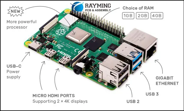
Raspberry Pi 4 – Big upgrade in 2019 to a 1.5GHz quad-core Cortex-A72 CPU, options for 1GB-8GB RAM, USB 3.0, dual monitor support via micro HDMI. Huge leap in performance.

Raspberry Pi 400 – All-in-one Pi integrated into a compact keyboard launched in 2020. Based on Pi 4 compute module.

Raspberry Pi Zero/Zero W – Tiny and ultra low cost Pi models from 2015-2017 with a 1GHz single-core CPU and 512MB RAM.

There are also variants like the Compute Module and industrial models. But this covers the major mainstream Raspberry Pi boards. The Pi 4 provides the most powerful and versatile experience currently.

Now let’s look at some key specs that enable all the Pi’s capabilities.

Raspberry Pi Specifications and Capabilities

Here are some of the most important technical capabilities of the Raspberry Pi hardware and platform:

  • CPU: Modern quad-core ARM processors around 1.5GHz, capable of 32-bit and 64-bit operation. Provides good overall performance for a low-cost board.
  • RAM: 1GB to 8GB LPDDR4 RAM on Pi 4. Important for running desktop OSes and applications.
  • GPU: Powerful integrated graphics supports 1080p video encoding/decoding, OpenGL ES, and flexible display output.
  • Video Output: Dual micro HDMI ports support up to 4Kp60 resolution. Composite video and DSI display outputs also available.
  • Audio: Stereo audio over HDMI or via 3.5mm headphone jack.
  • Networking: Gigabit Ethernet, 802.11ac WiFi, Bluetooth support.
  • USB: 4x USB 2.0 ports, 2x USB 3.0 ports on Pi 4 for ample peripheral connectivity.
  • Storage: MicroSD card slot for loading OSes and storing data.
  • GPIO Pins: 40 flexible GPIO pins to interface with electronics projects.
  • Camera/Display Ports: Integrated camera and display interfaces make it easy to add those modules.
  • Peripherals: Optional hardware like official 7″ touchscreen, case fans and more available.
  • Operating Systems: Can run various Linux distros, Windows 10 IoT, Android Things, and more.
  • Programming: Support for Python, Scratch, C/C++, Node.js, Bash, and many other languages.

This combination of capabilities makes the Pi extremely well-suited for a wide range of applications, as we’ll now explore.

Common Raspberry Pi Operating Systems

One strength of the Raspberry Pi is the ability to run different operating systems based on your needs. Here are some of the most popular OS choices:

Raspberry Pi OS (formerly Raspbian) – The official Debian-based Linux distribution. Recommended starting point.

Ubuntu – Popular Linux distro with desktop and server builds for Pi. Great support.

Windows 10 IoT – Run Windows 10 on your Pi for familiar development environment.

RetroPie – Distro focused on retro gaming emulation. Good for entertainment center builds.

OSMC – Media center focused Linux OS to transform your Pi into a streaming box.

Lakka – Another Linux retro gaming distro similar to RetroPie.

Android Things – Stripped down Android OS from Google for IoT applications.

Twister OS – Raspberry Pi OS fork adding optimizations and additional software.

Manjaro ARM – Arch Linux-based distro designed to be fast and efficient on the Pi 4.

There are also specialty distributions for privacy-focused routing, media playback, enterprise applications, and more. The flexibility to choose different operating systems helps enable different use cases. Now let’s look at programming options.

Programming Languages and Platforms

Raspberry Pi 4
Raspberry Pi 4

The Raspberry Pi supports many programming languages and environments for building software applications and scripts:

Python – Very popular high-level language with huge ecosystem of Pi-focused libraries. Often the first choice.

Node.js – For creating network applications and web servers using JavaScript runtime.

C/C++ – Low level languages with access to hardware capabilities and high performance.

Java – Robust general purpose language well supported on the Pi.

Go – Compiled language gaining popularity for systems programming on Raspberry Pi.

Bash – Standard shell scripting language on Linux to automate tasks and access system functions.

.NET Core/.NET 5 – Run .NET apps with C# or Visual Basic using latest .NET runtime.

Scratch – Graphical programming environment designed to teach kids coding basics.

With this diverse range of supported languages, developers can build virtually any type of application on the Pi. Combined with GPIO pin access, USB ports, onboard video/audio, and accessories, the possibilities are endless!

Next let’s look at some of the most common ways people are using the amazingly versatile Raspberry Pi.

Media Center / Retro Gaming

One of the most popular uses for the Pi is creating customized home entertainment and retro gaming rigs. Its HDMI output, graphics capabilities, and GPIO pin access make it perfect for building your own media center.

You can install RetroPie, Lakka, or other distros to easily emulate games from classic systems like Nintendo, PlayStation, arcades, and more. Pair it with controllers, gaming buttons, a case, and TV connection for an all-in-one retro gaming machine.

For streaming media playback, OSMC is a great choice optimized for the Pi hardware with easy Kodi integration. Network your media files and play them easily.

With a compact form factor, cool case options, and near-silent operation the Pi makes for a slick living room addition for gaming and watching movies.

Networked Storage / File Server

The Raspberry Pi is often used as an inexpensive network attached storage (NAS) device or local file server. This takes advantage of the Ethernet/WiFi connectivity and microSD storage to share files on your network.

Using Samba and/or NFS allows easy mounting of the Pi’s storage from Windows, Mac, Linux machines. SSH provides secure remote shell access for easy administration.

You can also attach external USB drives for increased capacity. For more performance sensitive applications, you can boot the OS from USB 3.0 flash storage.

Overall, the Pi makes accessing shared storage and files simple and cost effective.

Web Server

With its wired and wireless network connectivity, the Pi also functions great as a web server using platforms like Nginx, Apache, Node.js, and more.

Developers can easily host websites and web apps on the Pi to experiment, learn about server administration, and conveniently access the content locally.

For production web serving, the Pi has limitations in performance and reliability versus a true server. But for personal and learning purposes, the Pi’s accessibility makes web hosting and server side development fun and practical.

Home Automation

Another common use case is home automation and IoT. The Pi’s GPIO pins allow easy interfacing with sensors, electronic components, and control systems.

Home Assistant is a popular open source automation platform with great Pi support. It allows monitoring sensors like temperature, controlling devices like lights and motors, automating routines, receiving notifications and more.

You can build one or more Pis into an automation hub to manage your smart home. The wireless and wired connectivity let the Pi communicate with various devices and cloud platforms.

IoT and Sensor Data Logging

Raspberry Pi 3A+
Raspberry Pi 3A+

For industrial IoT applications, the Pi works well at the edge capturing sensor data and interfacing with machinery.

It can connect to PLCs, analog sensors, serial devices, relays, motors, and digital logic easily using the GPIO pins. The Pi then logs data locally, pre-processes it, and transmits upstream.

The compact design also allows placing Pi’s with sensors in tight mechanical installations close to the monitored equipment.

Overall, the Raspberry Pi simplifies adding smarts and connectivity to industrial environments cost effectively.

Education and Learning

Education is a core part of the Raspberry Pi Foundation’s mission. The Pi has been transformational for teaching computing and IT skills to students of all ages.

Its hands-on nature, visual programming options like Scratch, and all-in-one design allows easily grasping electronics and programming basics. Lesson plans using the Pi are widely available.

Computing courses at schools and universities also use the Pi to teach operating system design, networking, security, and of course hardware interfacing skills.

It’s an affordable platform for computer science education and project-based learning. Students also learn Linux administration and practical troubleshooting skills using the Pi.

Robotics

The Pi provides an excellent integrated platform for robotics projects. Its small form factor suits mounting on mobile robots, drones, and robotic arms.

The GPIO pins allow interfacing with motors, servos, and sensors for automation and data capture. The quad-core processor can handle image processing and computer vision algorithms.

Popular robotics frameworks like OpenCV, TensorFlow, and Robot Operating System (ROS) all support the Pi. So developers have access to powerful libraries.

Affordable, packed with capability, and easy to mount, it’s no surprise the Pi has become ubiquitous in the DIY robot builder scene.

Arcade Cabinet

Retro gaming is so popular on the Pi that people build entire arcade cabinet rigs around it. By pairing the Pi with arcade controls, push buttons, an LCD panel in a customized cabinet, you can recreate the entire arcade experience at home.

Install RetroPie or a similar OS, add ROMs for all your favorite classic arcade games, and build an authentic looking cabinet for the full effect. It’s a fun electronics and woodworking project!

The Pi adequately powers even console systems like Nintendo 64 or PlayStation 1 for faithful on-screen gameplay. You can make it as elaborate as you like with marquees, artwork, speakers, etc. A weekend project that turns into a gaming masterpiece.

Security Camera

Leveraging the Pi camera module, you can construct a security camera or surveillance system. Simply add a camera to your Pi, configure streaming and recording software, and place it anywhere that needs monitoring.

MotionEyeOS or the official Pi OS work well out of the box for security camera use. You can also broadcast the stream over the network, record it to shared storage, or save locally on each Pi’s SD card.

The Pi camera supports night vision and higher resolution lenses for capturing detail. Overall, it provides an affordable yet capable backbone for a scalable multi-cam system.

VPN Server / Router

The Pi can serve as a cost effective, low power VPN server using implementations like OpenVPN or Wireguard. This allows securely accessing your home network remotely or tunneling traffic while on insecure public networks.

It’s also handy for running a Pi-hole ad blocking DNS server and Pi VPN server on the same device for privacy protection and removing ads anywhere.

For travel routers, Pi-based devices are compact yet powerful for sharing hotel and vacation rental internet connections securely with all your devices.

So the Pi pulls double duty well as a tiny private VPN server or travel router.

Weather Station

Building your own weather station is straightforward and fun with the Raspberry Pi. Various sensors can be added to collect temperature, pressure, rainfall, wind speed, lightning detection, and more.

The Pi gathers data from all the sensors and can push it upstream to weather services or your own database. It can also drive local dashboard displays to show current conditions.

Sense HAT add-ons make collecting sensor data like environmental readings very easy. The Pi easily creates a full-featured backyard weather monitor.

Smart Mirror

A smart mirror powered by a Raspberry Pi hidden behind a two-way mirror is a creative IoT project. Using a touchscreen lets you interact with the mirror to view news, weather, calendars, todo lists and more.

It provides a central smart home dashboard and easy access to information for your day in an innovative way. Voice control can also be added for hands-free interaction.

While fun to build, it’s also practical as an informational hub mounted in your bathroom, bedroom, or kitchen. A fully-customized smart home assistant designed just how you want.

Cluster Computing

The affordability of the Pi allows forming surprisingly powerful clusters with dozens or even hundreds of nodes. These provide low cost access to high levels of parallel computing power.

Clusters of Raspberry Pis are great for learning about distributed computing while also serving real workloads for research, universities, and hobbyist experimentation.

Kubernetes and Docker Swarm can orchestrate containers across a Pi cluster to run microservice-based applications. With LEGO cases and network wiring, you can build supercomputing-like setups on your desk.

Pi Laptop

For the ultimate portable Pi experience, one popular project is creating a Raspberry Pi laptop. This transforms your Pi into a custom mobile computer.

By integrating a display, battery pack, keyboard, and other peripherals into a case, you can make a Pi-powered laptop. Some kits are even available.

It makes for a fun electronics project while resulting in a practical portable device. With 8GB RAM, the Pi 4 has enough memory to run main desktop OSes like Raspberry Pi OS for a proper laptop experience.

The options and versatility of the Pi enable all kinds of creative computing projects like this.

Accessories and Add-Ons

The Pi foundation and third parties offer various official and unofficial accessories to expand the capabilities of the Pi in your projects:

  • Official 7″ Touchscreen – Fully integrated monitor with touch support.
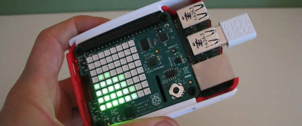
  • Sense HAT – Board with sensors and 8×8 LED matrix.
  • Camera Modules – Official 5MP and 8MP camera units for photos/video.
  • Pibow Cases – Unique multi-color 3D printed enclosures.
  • Pimoroni – Wide range of fun add-ons like light strips, audio cards, sensors, and more.
  • PiJuice – Uninterruptible power module for continual operation during outages.
  • Snap360 – Camera mount for capturing 360 degree photo spheres.
  • Fan SHIM – Integrated fan with programmable speed control.

The ecosystem of add-ons help tailor your Pi precisely for specialized applications. The sky’s the limit!

Limitations of the Raspberry Pi Platform

While remarkably capable, the Pi does have some limitations to keep in mind:

  • Performance – Can struggle with heavy multimedia workloads sometimes. Not a powerhouse.
  • Memory – 1GB base RAM on older Pis is quite constrained. 8GB on Pi 4 helps tremendously.
  • Storage – booting from microSD cards is slow. USB SSD helps, but not as fast as laptop drives.
  • Peripherals – Limited USB ports makes connecting lots of accessories difficult. Hubs help.
  • Power – Maximizing capabilities draws more electrical power. Careful component selection required.
  • OS Support – Some newer operating systems no longer maintain older Pi compatibility.

So while extremely versatile, the Pi cannot fully replace a high-end PC workstation or server for intensive tasks. But it covers 80% of use cases remarkably well!

Frequently Asked Questions

Here are some common questions that arise when using the Raspberry Pi:

Q: Does the Raspberry Pi replace an Arduino or other microcontrollers?

A: The Pi is like an Arduino on steroids – more powerful CPU and OS, but lacks the precise timing and analog inputs of an MCU. The two are complementary depending on your specific needs.

Q: How difficult is the Raspberry Pi for kids to learn on?

A: Thanks to kid-friendly environments like Scratch and Python, the Pi is quite accessible for introducing children to programming. But may still require parental guidance below age 10.

Q: Which model Raspberry Pi should I get as a starter option?

A: The newer Raspberry Pi 4 Model B with 4GB RAM provides the best overall experience balancing cost, performance, and longevity. Avoid older models like the Pi 1 or Zero.

Q: Is overclocking the Raspberry Pi recommended for extra performance?

A: Overclocking is possible through config tweaks, but be careful! It voids your warranty and puts stability at risk. Modest overclocks may work but expect crashes if pushed too far.

Lead Free Solder Vs Lead Soldering: How to Choose in Electronics Use

Solder is an essential material used in electronics manufacturing to create mechanical and electrical connections between components and printed circuit boards (PCBs). Traditionally solder contained lead, but environmental concerns have driven wide adoption of lead-free solder alloys. However, lead solder still offers some advantages over lead-free alternatives in certain applications. This article compares properties, strengths and limitations of leaded and lead-free solders to help select the optimal type.

Overview of Lead and Lead-Free Solders

Solder is a metal alloy that liquifies at relatively low temperatures making it ideal for electronics assembly. It flows into the joint, then solidifies forming permanent electrical and mechanical soldered connections. Here is a brief overview comparing traditional lead solder versus modern lead-free solder:

Lead Solder

  • Contains 30-40% lead alloyed with tin
  • Melting point around 180-190ยฐC
  • Excellent wetting and flow characteristics
  • Relatively low cost
  • Toxic – restricted in some regions

Lead-Free Solder

  • Replaces lead with silver, copper, bismuth etc.
  • Higher melting point, typically 217-220ยฐC
  • More difficult wetting and flow
  • Higher cost than leaded
  • Reduced environmental impact

Both offer trade-offs that make each preferable for certain applications as we will examine in detail.

Why Choose Lead-Free Solder?

Lead-free solder alloys eliminate toxic lead to mitigate environmental and health hazards associated with electronics waste:

Reduced Environmental Contamination

  • Lead persits indefinitely and accumulates in the environment when electronics are improperly discarded in landfills. Lead-free solder reduces lead contamination risks.

Improved Worker Safety

  • Lead exposure negatively impacts personnel health. Lead-free solder helps protect assembly line staff from lead’s neurological and reproductive toxicity when handled regularly.

Complying With Regulations

  • Laws like the Restriction of Hazardous Substances (RoHS) directive ban lead solder from consumer electronics to reduce lead waste pollution. Most electronics OEMs have transitioned to comply.

Avoiding Lead Contamination

  • Lead can contaminate food processing equipment and medical devices leading to health risks. Lead-free solder prevents lead leaching.

Minimizing Disposal/Recycling Issues

  • Separating and properly recycling leaded waste adds cost. Lead-free products simplify end-of-life disposition.

For most new consumer product designs, lead-free solder is now standard. But in specialized cases, leaded solder still offers advantages.

Why Lead Solder Remains Advantageous

Despite the push towards lead-free electronics, leaded solder provides some ongoing benefits in certain applications:

Lower Melting Point

  • Lead solder melts around 180-190ยฐC versus 210-220ยฐC for lead-free. This allows use with heat sensitive components.

Improved Wetting and Flow

  • Lead alloys readily wet and spread on copper and component leads. Lead-free solder can require flux assistance.

Reduced Joint Cold Flow Stress

  • Softer lead solder reduces shear stresses on thermal cycle. Lead-free joints more prone to tin whiskering.

Lower Cost

  • The continued wide availability of tin-lead solder keeps costs modest. Some lead-free alloys utilize expensive metals.

Exemption for Defense/Aerospace

  • Mission critical military and avionics applications still permit lead due to reliability concerns.

Repairability

  • Leaded solder joints are easier to reheat for component replacement versus lead-free.

Lead solder remains preferable for many high reliability industrial, military, aerospace, and maintenance applications where its unique advantages outweigh toxicity concerns.

Lead-Free Solder Alloys

Lead-free solders most often consist of tin alloyed with metals like silver, copper and bismuth to mimic lead’s properties as closely as possible. Common compositions include:

SnAgCu (SAC) โ€“ Tin-Silver-Copper (95.5Sn/3.9Ag/0.6Cu)

  • Most popular lead-free alloy
  • Good mechanical properties
  • Prone to tin whiskering

SnCu โ€“ Tin-Copper (99Sn/0.7Cu)

  • High tin content improves ductility
  • High melting point of 227ยฐC

SnAg โ€“ Tin-Silver (96.5Sn/3.5Ag)

  • Contains costly silver
  • Susceptible to silver leaching

SnBi โ€“ Tin-Bismuth (42Sn/58Bi)

  • Lowest melting point of just 138ยฐC
  • Brittle with poorer thermal fatigue

SnZn โ€“ Tin-Zinc (91Sn/9Zn)

  • Zinc lowers melting point to 199ยฐC
  • Can corrode and weaken over time

SnAgBi – Tin-Silver-Bismuth

  • Contains silver for strength and bismuth for ductility

Alloy composition balances properties like melting point, joint strength, ductility, thermal fatigue and cost.

Comparison of Lead and Lead-Free Solder Properties

Here is how typical 63/37 tin/lead solder compares to common 95.5/3.9/0.6 Sn/Ag/Cu lead-free solder for key properties:

Property63Sn/37Pb95.5Sn/3.9Ag/0.6Cu
Melting Point183ยฐC217ยฐC
Electrical Conductivity15% IACS12% IACS
Thermal Conductivity35 W/mK60 W/mK
Coefficient of Thermal Expansion29 ppm/ยฐC23 ppm/ยฐC
Yield Strength16 MPa41 MPa
Elongation at Break40%40%
Creep ResistanceExcellentGood
Wetting CharacteristicsExcellentFair

Lead-free alloys compensate for drawbacks like higher melting point and poorer wetting through exact alloy adjustments and flux chemistries.

Mixing Lead and Lead-Free Solder

Ideally all soldering in a given product is done using consistent solder alloy to avoid incompatibility between joints:

  • Mixing leaded and lead-free solders risks formation of brittle intermetallic layers that weaken joints
  • Using lead-free solder over broader temperature profiles risks melting adjacent leaded solder joints
  • Matching solder alloy and flux core is optimal for wetting and flow

For niche cases allowing some mixed soldering, like repairing older electronics, observe these precautions:

  • Keep joint types isolated – leaded for repairs, lead-free for new soldering
  • Ensure the melting point of existing solder is 5-10ยฐC higher than the applied new solder
  • Use solder wick to fully remove previous solder before applying new alloy
  • Swap component leads if feasible to avoid soldering dissimilar alloys to the same leads

It is best practice however to standardize on one solder alloy per product during design when possible.

Lead Solder Application Notes

When working with traditional tin-lead solder:

  • Choose an alloy blend like Sn60/Pb40 or Sn63/Pb37 suited to the thermal needs
  • Specify flux-cored wire or paste for easiest application
  • Use the lowest temperature producing good flow to minimize thermal stress
  • Allow adequate cool down time since leaded solder remains molten longer
  • Employ adequate fume extraction due to lead vapor exposure risks
  • Follow safe lead handling procedures to avoid ingestion or skin contact
  • Properly label any product containing lead for recycling/disposal

With careful handling, lead solder remains an appropriate choice for high reliability industrial electronics not subject to RoHS regulations.

Lead-Free Solder Application Notes

To successfully apply lead-free solders:

  • Select alloy suited to process capabilities, like Sn/Ag/Cu or Sn/Cu
  • Use solder specifically formulated for lead-free use
  • Increase process temperatures to reach higher melting point
  • Adjust dwell times to achieve proper wetting with lead-free alloys
  • Use sufficient flux designed to eliminate lead-free processing issues
  • Review any component specifications for lead-free soldering suitability
  • Follow cleaning processes to remove all lead-free flux residues

With process adjustments, lead-free solders can deliver sufficient joint strength and reliability.

Lead-Free Solder Rework and Repair

Reworking and repairing lead-free solder joints raises challenges:

  • Higher melting point makes removal more difficult
  • Leaded solder should not contact lead-free joints
  • Traces may delaminate if overheated
  • Preheating is essential to minimize thermal shock
  • Flux must be thoroughly cleaned afterwards

Methods to rework lead-free solder connections:

  • Use hot air tool, mini soldering iron, or reflow oven
  • Preferentially heat component and junction, not entire board
  • For BGAs, use hot air nozzle following profile specifications
  • Remove all previous solder first before re-applying fresh solder

With care, lead-free solder joints can be successfully reworked or repaired.

Selecting Lead or Lead-Free Solder

Use lead solder when:

  • High reliability is critical – aerospace, military, automotive
  • Repairability and long service life are needed
  • Heat-sensitive components prohibit higher temperatures
  • RoHS regulations do not apply to the product
  • Process is already optimized for lead solder

Use lead-free solder when:

  • Consumer safety from lead contamination is paramount
  • Adhering to RoHS regulations for commercial products
  • Establishing an environmentally friendly process
  • Heat-resistant components permit higher temperatures
  • New process development allows optimizing for lead-free

Evaluate criteria like temperature limits, reliability, regulation, environmental impact and manufacturability when selecting solder alloy. With attention to detail, both leaded and lead-free solder can produce robust joints.

Summary of Lead vs. Lead-Free Solder Trade-Offs

  • Lead solder offers a lower melting point and superior wetting and ductility but carries toxicity concerns.
  • Lead-free solder eliminates lead risks but requires higher temperatures, precise alloying and well-controlled processes.
  • Each option has benefits making it preferable for particular applications subject to different technical and regulatory constraints.
  • Electronics assemblies should ideally standardize on consistent lead or lead-free solder, not mix alloys.
  • With well-developed processes, both solder alloy families can achieve excellent, reliable solder connections.

Understanding the trade-offs helps designers select the right solder type for each product based on performance, safety, reliability and other requirements.

Frequently Asked Questions

60 40 Vs 63 37 Solder

What are the most widely used lead-free solder alloy compositions?

The most common lead-free solder alloys used in electronics are:

  • SnAgCu (95.5Sn/3.9Ag/0.6Cu)
  • SnCu (99Sn/0.7Cu)
  • SnAg (96.5Sn/3.5Ag)
  • SnBi (42Sn/58Bi) – for very low melting points

Engineers select different ratios based on properties needed like melting point, strength, cost, and manufacturability.

Is lead-free solder always required? Are any exemptions allowed?

Lead solder remains permissible in:

  • Aerospace, military, and high reliability applications
  • Maintenance and repair of existing leaded electronics
  • Certain high temperature electronics
  • Applications exempt from RoHS regulations

If lead contamination is not a concern, leaded solder can still offer advantages.

What can mitigate the higher melting point challenges of lead-free solder?

Methods to conquer lead-free solder’s higher melting point include:

  • Adjusting process temperature settings higher
  • Lengthening dwell times over joints
  • Usingria appropriate soldering iron tip sizes/temps
  • Employing profiling techniques like ramp-soak-spike
  • Selecting alloy compositions with lower melting points
  • Verifying components meet higher temperature needs

With robust process development, reliable lead-free soldering is certainly achievable.

Via Filling in PCB Design: Key Techniques for Reliable Fabrication

A VIA hole in a PCB

PCB via filling is a critical manufacturing technique where plated through-holes are filled with either conductive or non-conductive material. This process enhances circuit board reliability by preventing air or liquid entrapment, reducing the risk of defects in demanding applications.

What is Via Filling?

Via filling is a process used in PCB manufacturing to enhance the reliability and performance of vias – the small holes that connect different layers of a multilayer PCB. These holes are typically plated with conductive material to create electrical connections between layers. However, in some cases, especially in high-density interconnect (HDI) boards or boards subject to harsh environments, simply plating the vias isn’t enough.

Via filling involves completely or partially filling these holes with conductive or non-conductive materials. This process serves several purposes:

  1. Improving thermal management
  2. Enhancing structural integrity
  3. Preventing contamination
  4. Enabling via-in-pad designs
  5. Improving the overall reliability of the PCB

Read more about:

Types of Via Filling

There are two main types of via filling used in PCB manufacturing:

Conductive Polymer Filling

Conductive polymer filling involves using a conductive material, typically a mixture of epoxy resin and conductive particles like copper or silver, to fill the vias. This method maintains the electrical connectivity between layers while providing additional benefits:

  • Enhanced current-carrying capacity
  • Improved thermal management
  • Better mechanical strength

Conductive filling is often used in high-power applications or when via-in-pad design is required.

Non-Conductive Via Plugging

Non-conductive via plugging uses non-conductive epoxy or resin to fill the vias. While this method doesn’t contribute to electrical connectivity, it offers several advantages:

  • Prevents solder from wicking through the via during assembly
  • Improves planarity for surface mount components
  • Enhances the board’s structural integrity
  • Protects against contamination

Non-conductive filling is commonly used in applications where via-in-pad isn’t necessary, but improved reliability and manufacturability are desired.

Cost Considerations for Conductive and Non-Conductive PCB Via Filling

The cost of via filling can vary significantly depending on several factors. Understanding these can help in making informed decisions during the PCB design process.

4 Factors That Affect the Via-Filling Cost

1. Hole Count

The number of vias that need to be filled directly impacts the cost. More holes mean more material and more processing time, leading to higher costs.

2. Type of Paste

The material used for filling affects the cost. Conductive pastes, especially those containing precious metals like silver, are generally more expensive than non-conductive options.

3. Manufacturing Complexity

The complexity of the PCB design, including factors like board thickness, via size, and aspect ratio, can influence the difficulty of the filling process and, consequently, the cost.

4. Testing and Quality Control

Rigorous testing and quality control measures are essential to ensure proper filling and reliability. These additional steps contribute to the overall cost but are crucial for producing high-quality PCBs.

Alternative Budget-Friendly Via-Filling Techniques

For projects with tighter budgets, alternative techniques can be considered:

Advantages of Via Fill Plug with LPI Solder Mask

Liquid Photoimageable (LPI) solder mask can be used to plug vias, offering a cost-effective alternative to traditional filling methods. Advantages include:

  • Lower material costs
  • Simpler manufacturing process
  • Adequate protection for many applications

Disadvantages of the Via Fill Plug with LPI Solder Mask

However, this method has some limitations:

  • Less reliable than traditional filling methods
  • Not suitable for via-in-pad designs
  • May not provide sufficient protection in harsh environments

Reducing Via Fill Costs in High-Volume Productions

For high-volume production, consider these cost-effective techniques:

Via Fill Plug

This method involves partially filling the via with conductive or non-conductive material, then covering it with solder mask. It’s less expensive than complete filling while still providing many benefits.

Plate Shut

For smaller vias, plating the hole until it’s completely closed can be a cost-effective alternative to filling. This method works well for vias with diameters less than 0.3mm.

Fab Notes for Via Filling

When specifying via filling in your PCB design, clear and detailed fabrication notes are crucial. Here are some key points to include:

  1. Specify the type of filling material (conductive or non-conductive)
  2. Indicate which vias need to be filled (all vias, specific sizes, or locations)
  3. Specify the filling method (complete fill, partial fill, or cap plating)
  4. Include any specific requirements for planarity or void percentage
  5. Reference relevant IPC standards

Clear fab notes ensure that your design intent is accurately communicated to the PCB manufacturer, reducing the risk of errors and misunderstandings.

IPC 4761 Standards for Via Filling and Via Covering

The IPC 4761 standard provides guidelines for via protection in PCBs. It defines seven types of via protection:

  1. Type I: Tented (Single Side)
  2. Type II: Tented (Double Side)
  3. Type III: Tented and Covered (Double Side)
  4. Type IV: Plugged
  5. Type V: Plugged and Covered
  6. Type VI: Capped
  7. Type VII: Filled and Capped

Understanding these standards and specifying the appropriate type in your design documentation ensures that your PCB manufacturer follows industry-recognized practices for via protection and filling.

How Do You Fill Vias During PCB Manufacturing?

The via filling process can vary depending on the specific requirements of the PCB design. Here are two common scenarios:

Filling of Via-in-Pad

Via-in-pad designs require complete filling of the via to create a flat surface for component placement. The process typically involves:

  1. Cleaning the via to ensure good adhesion
  2. Injecting conductive or non-conductive paste into the via
  3. Curing the filling material
  4. Planarizing the surface to ensure flatness
  5. Plating over the filled via to create a solderable surface

Filling of Microvias in HDI Boards

Filling microvias in HDI boards requires precision due to their small size. The process often includes:

  1. Carefully controlling the amount of filling material to avoid overfill or underfill
  2. Using specialized equipment designed for microvia filling
  3. Implementing strict quality control measures to ensure complete filling without voids

Via Filling Methods

There are two primary methods used for filling PCB vias:

1. Copper Plating

Additional copper electroplating is used to fill via holes fully with copper after initial plating:

  • Electrolytic process deposits copper inside drilled holes
  • Repeated cycles build up copper thickness
  • Copper grows evenly around barrel walls
  • Continues until via hole is 100% filled

Plating helps ensure uniform copper fill quality and reliable connections. But plating equipment represents a significant capital cost.

2. Conductive Ink Filling

Liquid solder masks or conductive inks are used to fill via interiors:

  • Allows filling vias after drilling
  • Ink injected by dispensing, stencil printing or other deposition
  • Fills multiple vias simultaneously
  • Inks cure when heated after board fabrication

Conductive inks provide a lower cost, more scalable via filling solution. But even ink filling can be challenging without optimized processes.

Now letโ€™s examine popular materials used for filling vias.

Via Filling Materials

Common materials used to fill PCB vias include:

Electroplated Copper

  • Pure copper fills via through electroplating
  • Excellent conductivity (IACS 100%)
  • Readily bonds with copper barrel
  • Reliable, uniform filling results
  • Higher equipment costs

Electroless Copper

  • Auto-catalytic copper deposition
  • Slightly lower conductivity than pure copper
  • Cannot build up thickness as much as electroplating
  • Provides conformal coating over hole walls
  • Lower cost technique

Solder Mask

  • Liquid photoimageable solder mask ink
  • Cures into solid epoxy fill when heated
  • Relatively high resistivity depends on filler metals
  • More prone to voids without process controls
  • Lower cost method

Conductive Epoxy

  • Two-part conductive epoxy adhesives
  • Filled with silver, carbon or nickel particles
  • Moderate conductivity depends on filler type/load
  • Can be dispensed or stencil printed into vias

The optimal via filling material balances electrical, thermal, reliability, and manufacturing cost considerations.

Failure Analysis of Filled Vias

Despite best practices, filled vias can sometimes fail. Understanding common failure modes can help in designing more reliable PCBs:

1. Fractures in the Via Wall Create an Electrical Discontinuity

Thermal stress or mechanical shock can cause fractures in the via wall, leading to open circuits. Proper design considerations, such as using more flexible filling materials or implementing stress-relief features, can mitigate this risk.

2. Voids in Filled Vias Cause Reliability Issues

Air pockets or voids in the filling material can lead to reliability problems. These voids can expand under heat, causing the filling to crack or separate from the via wall. Strict process control and quality inspection are essential to minimize void formation.

3. Environmental Impurities Can Result in Voids

Contamination during the filling process can create voids or weak spots in the filling material. Maintaining a clean manufacturing environment and using high-quality materials are crucial for preventing this issue.

4. An Imbalanced Plating Process Can Cause Voids

In plated vias, an imbalanced plating process can lead to uneven plating thickness or voids. This can compromise the electrical and mechanical integrity of the via. Proper control of plating parameters and regular maintenance of plating equipment are necessary to ensure consistent results.

Conclusion

Via filling is a critical process in PCB manufacturing that significantly impacts the reliability and performance of electronic products. By understanding the types of via filling, cost considerations, manufacturing processes, and potential failure modes, PCB designers and manufacturers can make informed decisions to create high-quality, reliable boards.

Whether you’re working on a high-density interconnect board for a cutting-edge mobile device or a rugged industrial control system, mastering the art of via filling is essential for success in today’s competitive electronics industry. By following industry standards, implementing best practices, and staying informed about the latest techniques, you can ensure that your PCB designs meet the demanding requirements of modern electronic applications.

What is PCB ink?

Introduction

Printed circuit board (PCB) manufacturing relies on depositing and patterning conductive materials to form the traces and features that carry signals and power. The conductive pastes and liquids used to create these circuit patterns are referred to as PCB inks.

PCB inks consist of conductive particles suspended in an adhesive formulation. After deposition and curing, these inks make up the copper circuitry that connects components on a PCB. This article provides an in-depth overview of PCB inks including:

  • Composition and properties of typical PCB inks
  • Different ink types and characteristics
  • PCB fabrication processes utilizing inks
  • New developments in ink formulations
  • Advantages of ink-based circuit fabrication
  • Considerations when selecting and applying inks
  • Examples of practical PCB ink applications

Understanding PCB ink technologies and capabilities allows engineers to consider the optimal materials and processes to fulfill circuit fabrication needs.

Composition of PCB Inks

PCB inks contain two primary constituents:

Metal Particles – Small conductive metal particles, typically copper or silver, make up 50-90% of an inkโ€™s mass. The key properties of the metal particles include:

  • High intrinsic conductivity
  • Purity – oxygen-free highly pure metals
  • Particle shape – spherical, flakes or mixtures
  • Particle size distribution – sub-micron to tens of microns
  • Oxidation resistance – for stable shelf life

Adhesive Matrix – A polymer binder adheres the metal particles together and bonds the cured ink to the substrate. Key properties include:

  • Solvent compatibility – soluble for deposition
  • Cure chemistry – thermal, UV, moisture, catalyst
  • Flexibility – maintains conductivity during bending
  • Adhesion strength – bond to substrates
  • Decomposition temperature – for operating range

The proportions and properties of these two components fundamentally define the performance of a PCB ink. Different ink types make trade-offs between these constituents to achieve specific characteristics.

Types of PCB Inks

There are several varieties of PCB inks formulated for different applications and processes:

Silver Flake Inks

  • High solid loading (60-85%) of silver flakes
  • Low curing temperature
  • Best electrical conductivity but higher cost

Copper Particle Inks

  • Moderate solid loading (50-60%) of copper
  • Low oxidation provides optimal stability
  • Lower cost than silver but higher resistance

Nano Copper Inks

  • Copper nanoparticles under 100nm
  • Enables low-temperature sintering
  • High electrical performance

Nano Silver Inks

  • Extremely fine (<50nm) silver particles
  • Lower curing temperature while maintaining conductivity
  • Printable using inkjet methods

Carbon Inks

  • Small graphite or carbon black particles
  • Lower conductivity than silver/copper
  • Often used for resistive elements

Each ink type exhibits trade-offs between performance, process compatibility, shelf life and cost.

PCB Fabrication Processes Using Inks

PCB inks serve different roles across common fabrication processes:

Printed Electronics

  • Inkjet, aerosol, screen and pad printing all deposit tracks
  • Low-temperature curing forms circuits

Conformal Printed Circuits

  • Inks printed on 3D surface
  • Enable flexible physiques

Flexible Circuits

  • Inks cured on polyimide substrates
  • Withstand bending and flexing

Additive Circuit Formation

  • Inks printed on PCB substrates
  • Add high density interconnects

Selective Plating

  • Ink masking layer defines plating areas
  • Removed after plating

EMI Shielding

  • Conductive inks add shielding to enclosures
  • Protects electronics

Inks provide versatility across diverse PCB manufacturing processes spanning printed electronics to plating to conformal circuits and more.

Advances in PCB Ink Formulations

Ongoing research and development continues expanding PCB ink capabilities through:

Lower Curing Temperature

  • Enables printing on temperature-sensitive substrates
  • Prevents component damage during curing

Finer Particles

  • Reduces required curing temperature
  • Provides higher resolution printing

Hybrid Particle Shapes

  • Tailor viscosity, densification and sintering
  • Optimize printing and electrical characteristics

Graphene Inks

  • Imparts flexibility, thermal conduction
  • Potential for lower costs

Copper and Nickel Inks

  • Alternatives to costly silver inks
  • Nearly matching electrical properties

Biocompatible Inks

Innovation in ink chemistry and materials science unlocks new potential applications.

Considerations When Selecting PCB Inks

Key considerations when choosing a PCB ink include:

Printing Method

  • Inks are formulated specifically for deposition techniques
  • Screen, inkjet, aerosol and other printing

Substrate Material

  • Adhesion strength varies with substrates
  • CTE matching prevents delamination

Curing Requirements

  • Ink curing method must match equipment
  • Temperature, UV, moisture, catalyst

Print Resolution

  • Particle size distribution affects achievable features
  • Finer particles enable smaller printed details

Shelf Life

  • Particle oxidation resistance impacts usable life
  • Refrigeration prolongs life

Operating Environment

  • Temperature, humidity, mechanical stresses
  • Ink must maintain performance across conditions

Properly matched ink, process and substrate produces optimal results.

PCB Ink Application Examples

Here are some examples of practical PCB ink applications:

Flexible Circuits

  • Silver polymer thick film ink printed on polyimide
  • Withstands repeated bending for wearable device

Conformal Antenna

  • Aerosol printed copper ink on curved surface
  • Enables non-planar smart device communication

Automotive Sensors

  • Copper ink printed circuits on polymer housing
  • Integrates PCBs into modules

Medical Patches

  • Biocompatible silver/graphene ink circuits
  • Adheres to skin for health monitoring

EMI Shielding

  • Silver ink applied inside device enclosure
  • Protects electronics from interference

Heater Elements

  • Highly resistive carbon ink printed on glass
  • Provides localized transparent heating

These examples illustrate the diversity of possibilities using printed inks for circuit fabrication.

Frequently Asked Questions

Here are some common questions that arise regarding PCB inks:

Q: What is the main trade-off between silver and copper inks?

Silver inks provide higher conductivity but at a higher raw materials cost, while copper offers a more affordable option with slightly higher resistivity.

Q: What are some methods used to deposit PCB inks?

Common methods include screen printing, inkjet printing, aerosol printing, flexographic printing and syringe dispensing.

Q: How small of circuit features can be produced using PCB inks?

The finest features range from 10-50 microns depending on the printing process resolution, particle sizes, and post-printing curing approach used.

Q: Do PCB ink patterns require plating for most applications?

Often yes, plating improves conductivity and durability. But some applications like embedded heating elements can utilize printed ink-only circuits.

Q: What are the shelf life considerations for PCB inks?

Shelf life varies based on formulation, with silver flake inks lasting 1-3 years refrigerated. Use within 6 months is recommended for optimal results.

Conclusion

PCB inks enable versatile printed circuit fabrication techniques spanning printed electronics, EMI shielding, heaters, sensors, and more. As ink formulations and printing processes continue advancing, ink-based circuit manufacturing empowers new design possibilities and applications. Understanding the composition, types, processes and properties of these conductive inks allows engineers to take full advantage of their capabilities and expand the horizons for PCB innovation.

Which is Better Low Frequency or High-frequency Inverter?

Introduction

Inverters convert DC power into AC power to operate AC equipment and devices. They utilize power electronic switching at different frequencies to generate the AC output. This articles examines low frequency inverters operating near the AC line frequency versus high frequency inverters using much higher switching frequencies. The comparative advantages and disadvantages are analyzed to determine which approach is better suited for different applications.

Defining Low and High Frequency Inverters

Low Frequency Inverters

  • Use switching frequencies close to 50/60Hz line frequency
  • Typically 100 Hz to 5 kHz range
  • Requires large inductors and capacitors

High Frequency Inverters

  • Switch at much higher 10s of kHz to MHz frequencies
  • Very high ratio between switching and output frequency
  • Allows use of smaller filter components

Frequency Ratio

  • Low frequency inverters have ratio of up to 1:100
  • High frequency inverters reach 1:1000 to 1:50,000 ratios

Low Frequency Inverter Operation

[Simple circuit diagram]

  • Full bridge topology commonly used
  • MOSFETs or IGBTs switched at line frequency rates
  • Large AC inductor filters output to smoothen waveform
  • Produces nearly sinusoidal voltage at line frequency

High Frequency Inverter Operation

[Simple circuit diagram]

  • Similar bridge topology used
  • Operates at much higher switching frequency
  • Smaller inductor and capacitor filters the output
  • Generate clean sine wave at desired line frequency

Comparison of Characteristics

ParameterLow Frequency InverterHigh Frequency Inverter
TopologyFull bridge usually usedMost use full bridge
Switching Frequency100 Hz to 5 kHz20 kHz to 1 MHz
Frequency RatioUp to 1:100Up to 1:50,000
Filter SizeLarge inductors and capacitorsSmall inductors and capacitors
SemiconductorsBJTs, MOSFETs, IGBTsMOSFETs, IGBTs
Control ComplexitySimpleComplex high-speed control
EfficiencyModerateVery high
Power DensityLowVery high
DistortionHigher harmonics presentLow harmonic distortion
Response SpeedSlowVery fast
Physical SizeLargeCompact
WeightHeavyLight
ApplicationsUPS, motor drives, PV invertersDrives, UPS, aircraft, medical

Low Frequency Inverter Benefits

Some benefits of low frequency inverters include:

Simplicity

  • Requires only basic controls for switching
  • Open loop voltage control is straightforward
  • Does not need specialized driver circuits

Robustness

  • High overload capacity due to larger components
  • Less affected by noise and temperature variations
  • High reliability and ruggedness

Low EMI

  • Very little high frequency interference generated
  • Minimal filtering needed for EMI compliance

Low Acoustic Noise

  • Any switching noise present at inaudible frequencies
  • Minimal acoustic noise issues

Lower Cost

  • Cost effective magnetic components
  • Simple semiconductor selection
  • Minimal additional circuitry needed

High Frequency Inverter Advantages

Salient advantages of high frequency inverters:

Compact Size

  • Extremely small due to high-frequency magnetics
  • High power density up to 50W/cubic-inch
  • Ideal for lightweight portable applications

Fast Response

  • Very fast transient response speed
  • Precise and agile control ability
  • Well suited for dynamic speed or voltage regulation

High Efficiency

  • Up to 97% efficiency achievable
  • Lower conduction and switching losses
  • Reduces running costs and heat sinking needs

Light Weight

  • Massive reduction in magnetics and filters
  • Superior power-to-weight ratio
  • Easier mounting and portability

Quiet Operation

  • Any audible noise pushed into ultrasonic range
  • Nearly silent operation suitable for occupied spaces

Disadvantages of Low Frequency Inverters

Some drawbacks of low frequency inverters include:

Large Size

  • Significant space needed for large inductors and capacitors
  • Limits applications with space constraints

Slower Response

  • Cannot quickly change output voltage or frequency
  • Not suitable for dynamic speed or voltage control

Distortion

  • May have considerable lower order harmonics
  • Additional filtering required for sensitive loads

Acoustic Noise

  • Audible noise around switching frequency
  • Irritating hum or buzz if in human audible range

Lower Efficiency

  • Hard-switched topology causes increased losses
  • Heat sinking needs add cost and size

Drawbacks of High Frequency Inverters

Some limitations of high frequency inverters:

Complexity

  • Requires sophisticated control methods and ICs
  • Challenging gate drive design for reliable switching
  • Overall system design complexity increased

EMI Issues

  • High frequency switching generates interference
  • Needs substantial EMI filtering

Reliability Concerns

  • Hard switching and thermal cycling degrade reliability
  • Device failure rates may be higher

Acoustic Noise

  • Ultrasonic losses need to be attenuated
  • Can cause issues with adjacent electronic systems

Higher Cost

  • Specialized high-speed devices increase costs
  • Additional circuits add expense
  • May require modular construction

Choosing Between Low and High Frequency Inverters

Low frequency inverters are advantageous for:

  • Simple low cost inverter designs
  • High reliability requirements
  • High overload capacity needed
  • Situations where EMI is detrimental
  • Applications with audible noise constraints

High frequency inverters are better for:

  • Very compact portable systems
  • Weight critical applications like aerospace
  • High precision fast response speed needed
  • High efficiency essential to reduce losses
  • Meeting tight harmonic distortion requirements

Conclusion

  1. Low frequency inverters are simpler, more robust and easier to control.
  2. High frequency inverters enable miniaturization, fast response, efficiency and ultra-quiet operation.
  3. The choice depends on the specific size, performance, cost, reliability and noise criteria for the application.
  4. Hybrid inverters running at medium frequencies can balance the tradeoffs.
  5. Advances in topology, modulation, devices and materials continue to improve low and high frequency inverter performance.

Frequently Asked Questions

What is the typical frequency range considered as “high frequency” for inverters?

Inverters operating from around 10 kHz up to 1 MHz are considered high frequency, compared to low frequency inverters running under 5 kHz.

What are the main advantages of low frequency inverters?

Simplicity, ruggedness, low EMI, and low acoustic noise are some of the advantages of low frequency inverters. They also have higher overload capacity.

What semiconductor devices are commonly used in high frequency inverters?

MOSFETs, IGBTs, and new widebandgap devices like GaN transistors allow switching frequencies up to 1 MHz range for high frequency inverters.

What are some examples of applications suited for high frequency inverters?

Motor drives, uninterruptible power supplies, induction heating, avionics, EV charging, renewable energy integration favor high frequency inverters for their compact, lightweight and dynamic characteristics.

How does efficiency compare between low frequency and high frequency inverters?

Properly designed high frequency inverters can achieve over 97% efficiency by using advanced devices to minimize switching and conduction losses at higher frequencies.