RF PCB Design Guidelines You Must Know

Introduction

Designing printed circuit boards for radio frequency (RF) applications requires special considerations to ensure proper performance. At microwave and mmWave frequencies, the properties and layout of PCB materials have a major impact on parameters like loss, impedance control, and signal integrity.

This guide covers key RF PCB design guidelines and best practices. Following these will help RF boards achieve target behavior in terms of losses, spurious signals, power transfer, and other critical high frequency characteristics. Weโ€™ll examine stackup arrangements, layout techniques, grounded coplanars, material selection, simulations, and more.

Properly incorporating sound RF design principles results in PCBs delivering reliable, repeatable performance across fabrication variations and a wide array of operating conditions. Avoid surprises late in the development cycle by understanding these essential RF design guidelines up front.
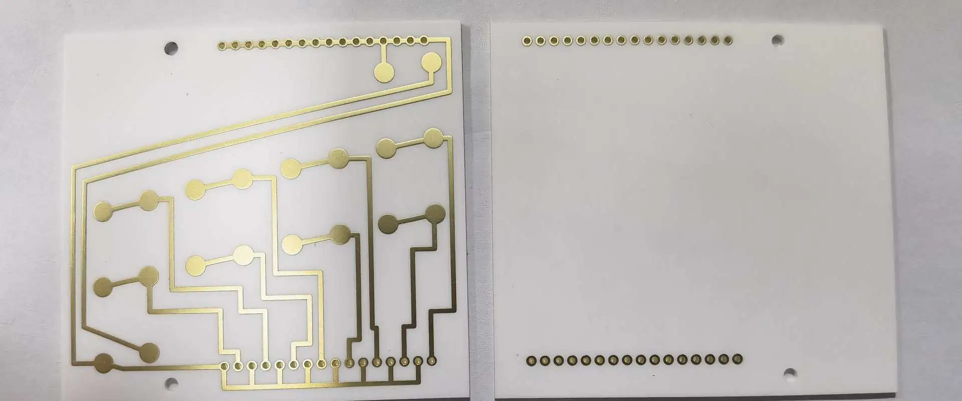
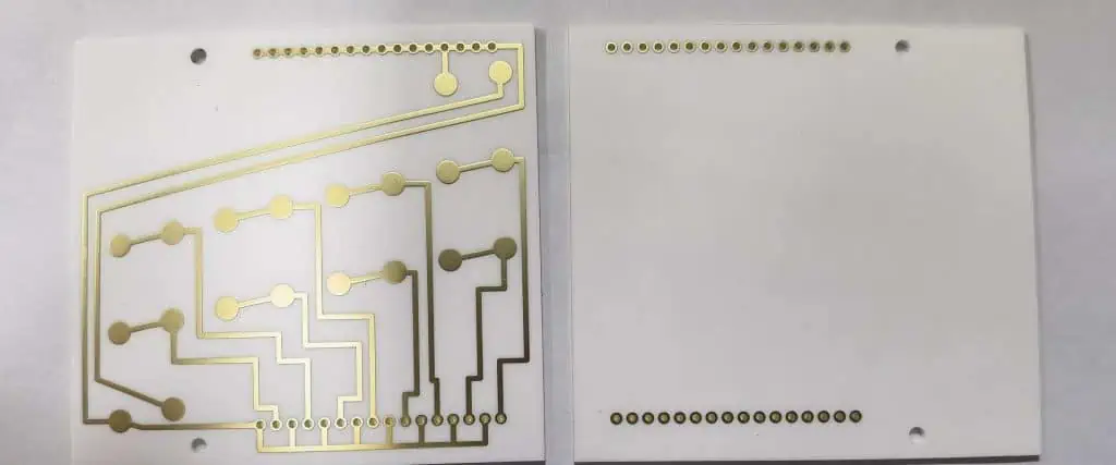
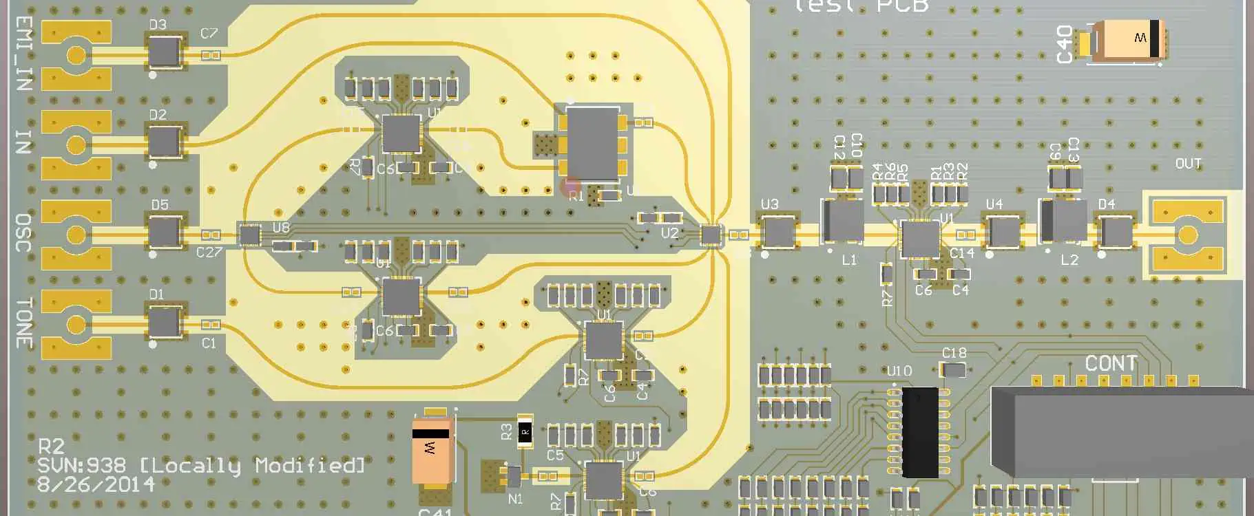
Stackup Arrangement

A properly planned layer stackup forms the foundation of any high performance RF PCB layout:

Use Thin Dielectrics

At higher frequencies, a thinner dielectric allows tighter impedance control and reduced loss per inch. Typical RF dielectrics are 2 to 4 mils thick.

Orient Core Grain Direction

Alternate the dielectric grain direction in subsequent cores to equalize dimensional stability. This prevents skewing during lamination.

Include Ground Planes

Ground planes provide an ideal continuous RF return path and shielding. Place them strategically to isolate different signals.

Embed Controlled Impedances

Sandwich controlled impedance traces between ground planes to enhance tuning and shielding.

Model Before Finalizing

Model the stackup in your RF simulation tool and optimize before committing to a configuration. Tweak dielectrics, copper weights, and arrangements as needed to refined the design.
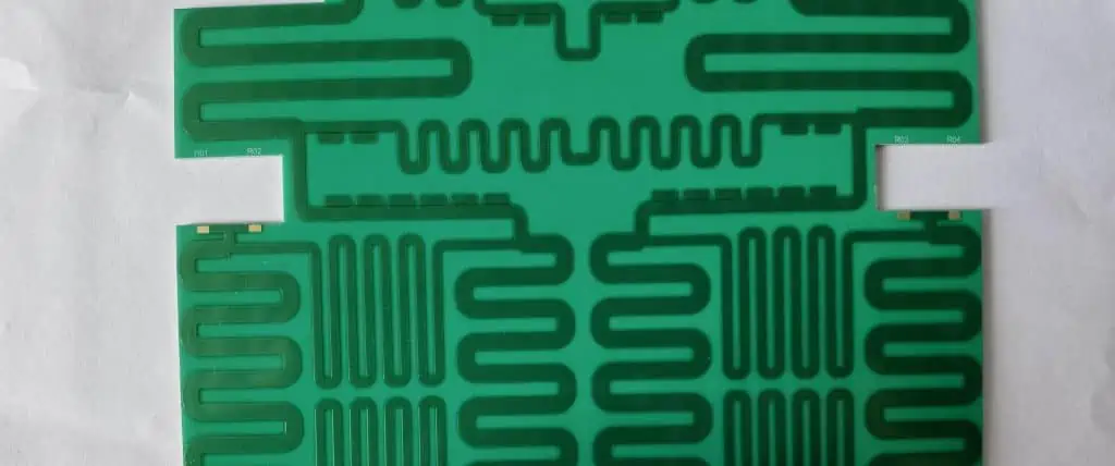
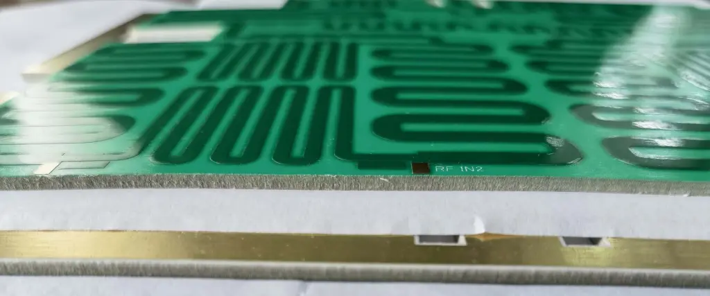
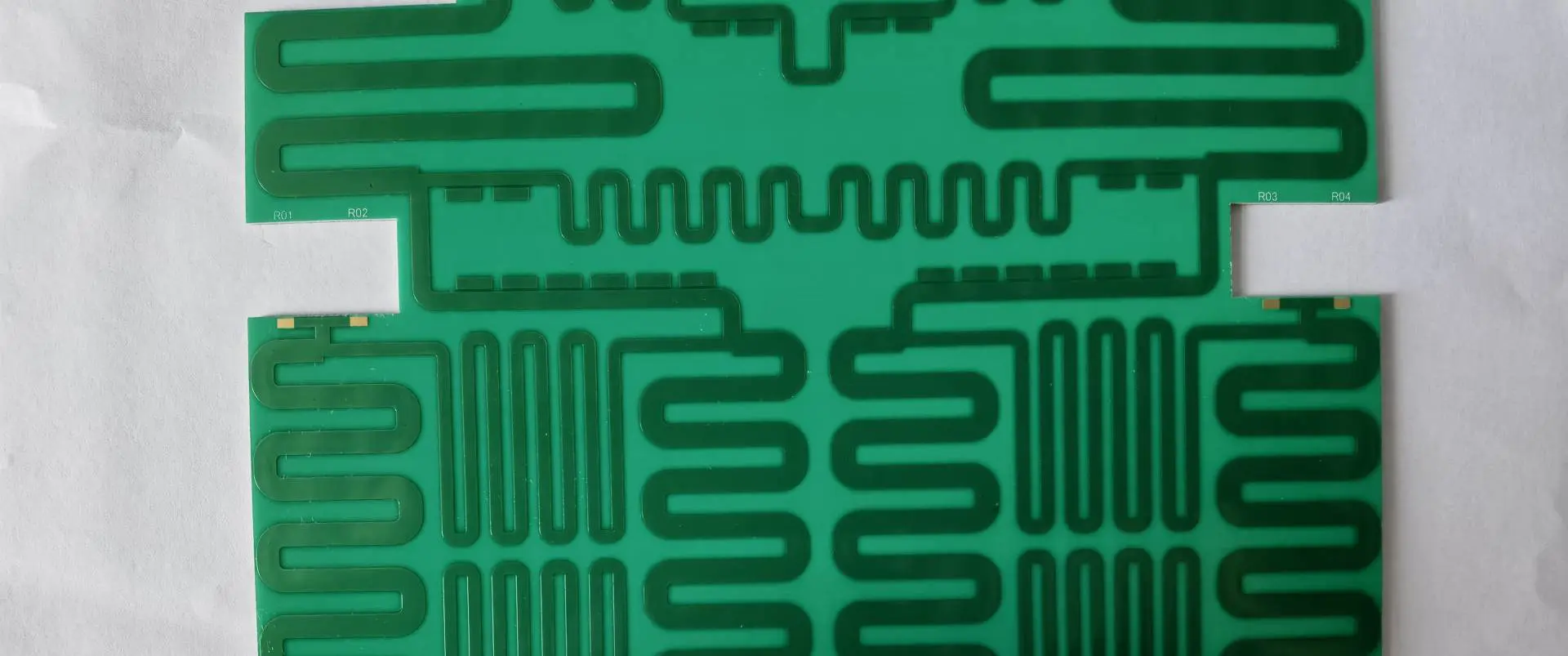
Transmission Lines

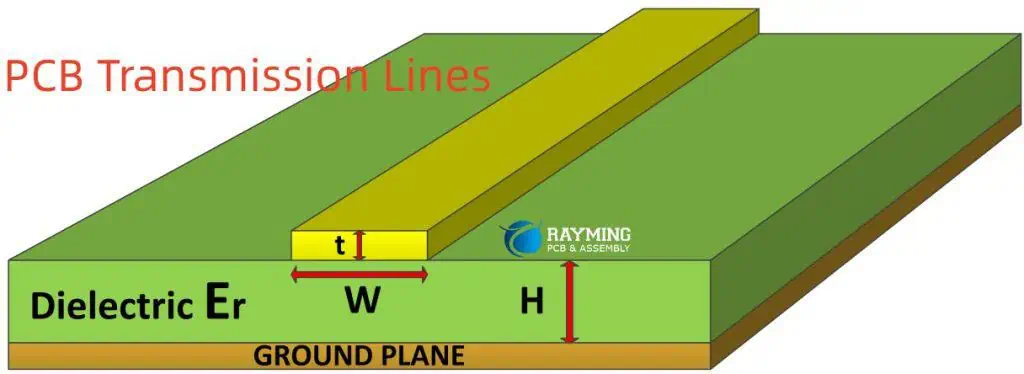
Transmission lines like microstrips and striplines carry high frequency signals across a PCB:

Matched Impedance

Use controlled impedance lines matched to system impedance (typically 50 ohms) to minimize losses.

Short Stub Lines

Keep stubs short to avoid unwanted capacitive coupling. Use vertical transitions where changes are unavoidable.

Smooth Wave Impedance

Taper impedance gradually over longer lengths for impedance matching and reduced reflections.

Terminate Lines

Properly terminate lines in their system impedance at the load end to prevent reflections from discontinuities.

Reflection-Free Bends

Avoid 90 degree bends. Use arc or mitered 45 degree bevels to reduce discontinuities in the wave impedance.

Coupled Lengths

When coupling lines, tightly control the gap and length ratio to achieve target coupling factors.

Careful application of transmission line theory is critical to RF PCB performance.

Grounded Coplanar Waveguides

Grounded coplanar waveguides involve placing signal traces between ground planes on the same layer. Benefits include:

  • Excellent shielding and isolation
  • Permits closer packing density
  • Reduces radiation losses
  • Allows easy shielding vias to ground
  • Supports high frequency millimeter-wave signals

Use coplanar techniques where stripline or microstrip won’t suffice for shielding or density needs.

Passive Components

RF passives require special attention during layout:

Place Near ICs

Keep passives physically close to their driving IC pins to avoid long stub traces.

Orient Perpendicular

Wherever possible, orient inductors and capacitors perpendicular to their attached traces. This avoids parasitics.

Flood Ground Around

Provide a flood ground fill around all passive components. This shields noise coupling and maintains low inductance.

Watch Spacing

mind spacing around passives to avoid coupling between components.

Model Libraries

Use vendor 3D models or EM-based parasitic models for passives for optimal simulation accuracy.

Careful passive layout minimizes parasitic effects that impair frequency response.

Material Selection

rogers substrate

Choosing suitable PCB materials is crucial for achieving target RF performance. Key considerations include:

Dielectric Constant

Select a dielectric constant to ensure proper impedance. Variability risks impedance mismatches.

Loss Tangent

Lower loss materials like PTFE reduce insertion losses for greater range and efficiency.

Moisture Absorption

Lower absorption coefficients minimize performance degradation in humid conditions.

Thermal Properties

Manage lamination stresses and match expansion coefficients to avoid electrical issues from physical warping.

Lead-Free Assembly

Use high Tg materials compatible with lead-free assembly processes necessary for commercial products.

Availability

Choose readily available materials with multiple qualified laminators to control supply chain risks.

There are always tradeoffs to weigh when selecting RF laminates.

Copper and Finishes

Like dielectrics, carefully selecting conductor materials enhances RF response:

Copper Weights

Heavier copper above 2 oz enables better power handling and low loss performance.

Rolled or Electrodeposited

Electrodeposited copper foils tend to provide smoother surface finishes.

Surface Roughness

Smooth copper foil reduces conductor losses at high frequencies due to skin effects.

Final Finish

Immersion silver or gold provide excellent surface conductivity while slowing tarnishing.

Plating Buildup

For heavy power traces, electroplated copper increases conductor thickness over foil alone.

Thermal Management

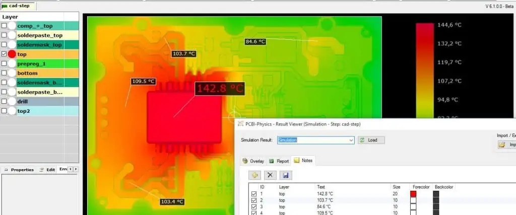
Poor thermal performance impacts RF PCBs through:

  • Electrical parameter variations with temperature
  • Mechanical warping inducing stress
  • Accelerated aging and material breakdown

Use Thermal Vias

Place thermal vias under hot components allowing heat conduction to inner and bottom layers.

Flood Planes

Use thick copper plane layers as heat spreaders where possible.

Heatsinks

Add localized heatsinks under high power devices if needed.

Air Flow

Permit sufficient air flow for convection cooling during enclosure design.

Thermal Modeling

Model thermal performance early to identify hotspots and refine layouts.

Proper thermal design prevents fluctuations and damage over the operating life.

Simulations

Accurately simulating RF boards requires using the appropriate tools:

EM Simulators

Full wave 3D EM simulation captures complex energy interactions between components.

Parasitic Extractors

Model detailed parasitic characteristics caused by pads, vias, traces, and ground planes.

Material Models

Leverage available laminate material models from manufacturers capturing frequency dependent performance.

PCB PDN Analysis

Analyze common and differential path impedances to predict noise coupling on board.

S-Parameters

Use s-parameters for components to capture frequency-based input/output behavior.

TDR Modeling

Time domain TDR simulation validates impedance control and dispersion.

Matching simulations to real measured results builds confidence in the PCB layout.

Conclusion

Following sound RF design principles enables PCBs operating reliably at microwave and mmWave frequencies. Paying attention to stackup arrangements, layout techniques, material selections, simulations, and other best practices prevents nasty surprises late in the development cycle. While RF design requires meticulous care, the methodical application of these guidelines results in high performance boards meeting their operating goals across all conditions.

Frequently Asked Questions

Q: At what frequency do RF design considerations for PCBs start to become necessary?

A: Most experts recommend treating any design over 1 GHz as an RF layout. However, techniques help even at a few hundreds MHz.

Q: What are some key software tools used for RF PCB design and simulation?

A: Popular options include Cadence Allegro, Mentor Xpedition, Keysight ADS, Ansys HFSS, and Altium.

Q: What are typical stackup layer counts for RF PCB designs?

A: High frequency boards trend towards 4-16 layers. This enables embedding controlled impedances between ground planes while avoiding overly thick dielectrics.

Q: How are impedance matched interconnects created on PCBs?

A: Carefully engineering the trace geometry and dimensions along with dielectric height relative to ground maintains target impedance like 50 ohms across a route.

Q: What are some common RF PCB laminate materials?

A: Popular options include Rogers RO4000, Taconic RF-35, Isola IS680, Arlon CLTE, and PTFE composites. These provide tightly controlled dielectric constants.

What is Aluminum Nitride PCB (AlN PCB)?

1050c ceramic board

Introduction

Aluminum nitride (AlN) PCBs refer to ceramic printed circuit boards made using aluminum nitride ceramic substrates instead of the standard FR-4 laminates. Aluminum nitride ceramics have excellent thermal conductivity, electrical insulation, and thermal expansion properties making them highly suited for demanding electronic applications.

This article provides an overview of AlN PCB technology including its benefits versus FR-4 boards, manufacturing processes, layout considerations, and applications where AlN PCBs provide the best performance and reliability.

Benefits of AlN PCBs

Aluminum nitride PCBs offer several advantages compared to conventional FR-4 boards:

  • Extremely high thermal conductivity (~170 W/mK) for superior heat spreading and dissipation
  • Thermal expansion matches silicon allowing direct chip attach methods
  • Electrically insulating with high dielectric strength and volume resistivity
  • Withstands very high temperatures (>1000ยฐC) with minimal mechanical distortion
  • Excellent dimensional stability and resistance to thermal shock
  • Low dielectric loss for high frequency operation
  • Compatible with common metallization techniques and soldering
  • Hermetic sealing possible for high reliability requirements
  • Resists moisture absorption and chemical corrosion
  • High strength provides resistance to mechanical stresses
  • Electrically isolates circuits and components on single board
  • Lightweight compared to most other ceramic substrates

These benefits make AlN PCBs ideal for power circuits, RF designs, and extreme environment applications.

Manufacturing AlN PCBs

Aluminum nitride PCBs are fabricated using the following general process steps:

Substrate Manufacturing

  • AlN powder is formed into a billet through cold isostatic pressing
  • Binder materials are added to facilitate handling of the material
  • The shaped billet is sintered at temperatures above 1800ยฐC in a nitrogen atmosphere
  • Sintering fuses the AlN powder into a fully dense ceramic
  • The AlN board is precisely ground and polished down to specified thickness

Metallization

  • Thick film pastes with tungsten or molybdenum are screen printed to form circuit traces
  • Thin film metals like copper or gold can also be deposited via sputtering or plating
  • High temperature firing bonds the metallization to the AlN substrate

Multilayer Buildup

  • Double sided boards are stacked and laminated with adhesive films
  • Vias and through holes are laser drilled and filled with conductive pastes
  • Blind and buried vias can connect between inner layers

Housing Integration

  • AlN substrates allow direct bonding into hermetic packages
  • Sealants like epoxy, braze or glass can be used

AlN PCBs fabrication leverages many of the same processes used for alumina ceramic boards but enables even higher performance thanks to the unmatched thermal conductivity.

AlN PCB Design Considerations

Here are some key design guidelines for aluminum nitride PCBs:

  • Traces should be 10 mils or thicker to ensure adequate conductor cross-section
  • Clearances of at least 8-10 mils required between adjacent traces
  • Via pads should be a minimum of 16 mil diameter or larger
  • Pad geometries may need adjustment from FR-4 designs
  • Gold plating often used for wire bonding pads
  • Match electrical and mechanical properties of all attached components and solder
  • Hermetic seals may impose height restrictions on components
  • Model thermal expansion effects when attaching large dies
  • Leverage thermal vias underneath hot devices
  • High frequency performance further improved with ground planes

Careful accounting of material behaviors, fabrication processes, and assembly procedures allows unlocking the full potential of AlN PCBs.

AlN PCB Applications

Some of the common applications leveraging aluminum nitride PCB technology include:

  • High power density electronics such as converters and inverters
  • Electric vehicle power systems and charging stations
  • High intensity LED systems
  • RF amplifiers, filters, antennas
  • Space and satellite electronics
  • Downhole drilling tools
  • Physics research instrumentation
  • Medical lasers and thermal therapy
  • High temperature electronics and sensors
  • Nuclear instrumentation and radiation detection
  • Automotive radars and LiDAR
  • Aerospace avionics
  • Hybrid microcircuits

For applications requiring management of high temperatures and thermal loads, AlN substrates enable packing the highest power densities thanks to best-in-class thermal conductivity.

Comparison to Alumina and FR-4

Aluminum nitride differs from alumina ceramics and FR-4 laminates in several ways:

ParameterAluminum NitrideAluminaFR-4
Thermal Conductivity170-200 W/mK24-30 W/mK0.25-0.5 W/mK
Dielectric Constant8.89.2-104.2-4.6
Dielectric Strength15-25 kV/mm10-15 kV/mm15-30 kV/mm
Temperature Resistance1000-1500ยฐC1000-1200ยฐC130-170ยฐC
CTE4.0 ppm/K6.5-7 ppm/K17-20 ppm/K
Flexural Strength330 MPa300 MPa180 MPa

Summary

  • Aluminum nitride PCBs provide extremely high thermal conductivity combined with electrical insulation.
  • Key manufacturing steps include sintering, metallization, lamination for multilayers, and integration into housings.
  • AlN enables high power density electronics due to unmatched heat spreading capabilities.
  • Thermal and mechanical behaviors require adjusted design rules compared to FR-4.
  • AlN PCB technology enables electronics to operate reliably in the most demanding temperature and power environments.

FAQ

What are some typical AlN PCB substrate thicknesses?

AlN PCBs typically range from around 0.5mm to over 2mm in thickness. Thinner boards maximize heat transfer while thicker variants offer better mechanical rigidity.

Can AlN PCBs be manufactured with multiple layers?

Yes, multilayer AlN PCBs can be fabricated by stacking double sided boards using adhesive films and integrating vias and through holes to interconnect layers. 4-6 layers can be achieved.

Is aluminum nitride fragile like traditional ceramics?

No, while hard, AlN has relatively high fracture toughness. It resists fracturing from impacts or drops better than traditional ceramics like alumina or glass.

What metal coatings are used on AlN PCBs?

Thick-film pastes with tungsten or molybdenum are common. Thin films like sputtered copper or plated gold allow high conductivity and wire bonding. Nickel is also used as a diffusion barrier.

Can AlN PCBs be machined and drilled like FR-4?

Yes, AlN can be machined, drilled, and routed but carbide tools are required. Diamond tooling provides highest precision. Coolant helps prevent tool heating and AlN cracking.

What is Alumina PCB ?

Introduction

Alumina PCBs are a type of ceramic printed circuit board made using aluminum oxide (Al2O3) ceramic as the substrate material instead of the more common FR-4 laminates. Alumina, also referred to as aluminum oxide, provides high thermal conductivity, electrical insulation, and excellent mechanical strength at elevated temperatures.

These properties make alumina PCBs ideal for applications requiring high power density electronics, thermal management, and survivability in harsh environments. The key benefits and applications of alumina PCBs are explored along with manufacturing processes and design considerations unique to alumina boards.

Benefits of Alumina PCBs

Some of the major advantages offered by alumina PCBs include:

  • High thermal conductivity (~30 W/mK) for excellent heat dissipation
  • Low thermal expansion provides reliable connections under thermal cycling
  • High strength and hardness resists fracturing and abrasion damage
  • Electrically insulating with high dielectric strength (>100V/mil)
  • Withstands very high temperatures (>1000ยฐC)
  • Inert material resists corrosion, radiation, and harsh chemicals
  • Supports layered circuitry and high component density
  • Customizable to achieve high precision geometries
  • Electrically isolates multiple circuits on a single board
  • Compatible with thick-film and thin-film metallization
  • Hermetic sealing possible for packages and housings

The combination of electrical, thermal, and mechanical properties make alumina substrates a top choice for specialized and high reliability PCBs.

Applications of Alumina PCBs

Some of the common application areas for alumina PCBs include:

Alumina boards can operate reliably in situations where conventional FR-4 based boards would fail due to thermal stresses or environmental conditions. The dielectric and thermal properties of alumina ceramic make it an excellent engineered substrate for specialized electronics.

Construction of Alumina PCBs

Alumina PCBs are fabricated by attaching metallized conductive patterns to a sintered and polished alumina ceramic baseplate. Here are some of the key fabrication steps:

Alumina Substrate Manufacturing

  • Raw alumina powder is molded and compressed into the required board dimensions
  • Binders are added to provide mechanical stability for handling
  • Firing at 1500-1600ยฐC sinters the pressed alumina into a monolithic structure
  • Cooling after sintering must be carefully controlled to prevent cracking
  • Final board is precision ground and lapped to achieve desired thickness and surface roughness

Metallization

  • Thick-film pastes containing metals like tungsten or molybdenum are screen printed onto the alumina and then fired at high temperature to form circuit traces
  • Thin-film metallization like sputtered titanium/copper can also create circuits patterns
  • Plating may be done to allow wire bonding or protect metals from oxidation

Multilayer Boards

  • Multiple double sided alumina boards can be laminated into a monolithic stack to build multilayer boards
  • Holes are laser drilled and then filled with conductive pastes to form vias between layers
  • Layer alignment maintained using guide pins and image recognition

Housing Integration

  • Alumina substrates allow direct integration into hermetic housings like ceramic DIP or LCC packages
  • Sealing done using brazing, epoxy adhesives, glass seals etc.

The excellent dimensional control and smoothness of the alumina ceramic baseplates results in high fidelity circuit patterns and reliable multilayer buildup.

Design Rules for Alumina PCBs

Alumina PCBs have tighter design constraints compared to conventional FR-4 boards:

  • Minimum trace/space is 5-10 mils versus 4-8 mils for FR-4
  • Maximum trace current is 15-25 A/mm of conductor width
  • Careful thermal matching with solders and metals required to avoid delamination
  • Via diameters start at 10 mils versus 6-8 mils for FR-4 boards
  • Component leads require sufficient compliancy to compensate for lower board flexure
  • Hermetic seals may limit component height restrictions
  • Components optimized for high temperature operation required
  • Thermal expansion mismatches between board, conductors, and components must be modeled
  • High frequency performance enhanced by design techniques like ground planes

While enabling improved reliability and environmental resilience, alumina PCBs require design adjustments from conventional board layouts to account for material behaviors and process differences.

Summary

  • Alumina PCBs utilize aluminum oxide ceramic substrates instead of the usual FR-4 laminates.
  • Alumina provides excellent thermal conductivity, temperature resistance, strength, and electrical insulation.
  • Key applications include high power, automotive, aerospace, oil drilling, military, and high temperature electronics.
  • Boards are fabricated by applying metallized circuits onto a sintered alumina baseplate. Multilayer builds also done.
  • Design rules accommodate lower flexure, higher processing temperatures, and material thermal expansion.
  • With proper design consideration for the material properties, alumina PCBs deliver superior performance and reliability in demanding applications.

FAQ

How does alumina PCB thermal conductivity compare to FR-4?

Alumina has a thermal conductivity around 30 W/mK compared to only 0.25 W/mK for standard FR-4 laminates. This provides far superior heat spreading and dissipation.

What are some typical thicknesses for alumina PCB substrates?

Alumina boards can range from around 0.25mm to over 1.5mm thickness. Thinner boards provide better heat transfer while thicker boards offer better strength for large boards.

Are alumina PCBs compatible with standard PCB assembly?

Specialized assembly is required including high temperature solders. Stress-engineered component leads help compensate for board rigidity. PCB coatings are used to prevent oxidation at elevated temperatures.

Does alumina absorb moisture like FR-4?

No, alumina is not susceptible to moisture absorption issues like FR-4 which can lead to outgassing and vapor pressure stresses under heat. Alumina retains its integrity.

Can multiple circuits or layers exist on a single alumina PCB?

Yes, multilayer boards can be fabricated by laminating together double sided boards, integrating passive components, and drilling/plating through hole vias. This allows complex circuitry.

Where to Print Easy PCB Cheaper

china pcb board manufacturer

PCB printing is an important aspect of PCB design. A circuit board is an important part of most electronic devices. Therefore, all aspects of manufacturing this board are very important. There are different factors that contribute to the cost of printing an Easy PCB. The type of software used will determine the cost of printing Easy PCB.

There are different programs designed to help you print Easy PCB cheaper. These programs offer you features that make it easy to print Easy PCB. Therefore, we will explain further on these programs.

Softwares that Print Easy PCB Cheaper

Design SparkPCB

This is free software for PCB design. With Design SparkPCB, you can get designs and 3D diagrams for closed conduits. Also, this software offers unlimited size of schematics. It can use several layers for a closed circuit.

In addition, this software features several PCB design tutorials. These tutorials help users familiar with Design SparkPCB. Also, this software is suitable for both beginners and experts. It also allows you to import and export files in your desired format. Also, you can create your own library if you donโ€™t want to use its extensive library.

KiCAD

KiCAD is open source electronics design software. This PCB design software can print Easy PCB. Also, it can create PCB layouts and electronic diagrams. It features a schematic editor and a PCB editor. The PCB editor can create PCB layouts with about 32 copper layers. KiCAD is free and doesnโ€™t require any paywall to utilize some of its features.

Also, this software has a component and schematic editor. There is also a footprint selector and a Gerber file viewer in this software.  Also, KiCAD features a project manager and a PCB calculator. It allows you to create footprints or components from bitmap images. KiCAD can run on Linux, Windows, and Mac. Also, you can run it with other distributions like Linux Mint and Ubuntu.

KiCAD has evolved overtime. The KiCAD Developers Team community manages this software. Also, this software is compatible with layer design and Schematic Capture. Also, it can obtain Gerber-type output files. Some of the most recent upgrades in this software include libraries for Path settings and 3D modeling. Also, it features Cairo canvas printing.

EasyEDA

FULL PCB MANUFACTURING Quote

This is special software designed for printing Easy PCB. EasyEDA is free software that offers a powerful schematic capture and libraries designer. Asides these features, this software offers a project management tool and a team collaborator.

Also, this software integrates with LCSC.com for offering real-time stocks. EasyEDA is a desktop and online based platform. Furthermore, EasyEDA is a cross-platform that supports Mac, Windows, and Linux.

Eagle

This is power PCB design software that allows you to print Easy PCB. Eagle is a new software designed by Autodesk. Also, this software provides powerful features and a great interface. It is very easy to use this software. Therefore, it is ideal for beginners.

Eagle features powerful modules like PCB editing, PCB printing, and schematic editing. This software can meet different PCB design demands. Also, Eagle allows you to modify a design and import information from other designs. In addition, this software offers a special feature known as automatic routing.

Eagle offers the following function:

  • Online backward and forward function
  • Interactive follow-up router
  • Importing of information from other designs and conversion to other formats

ExpressPCB Plus

This is EDA software that creates and designs PCBs. ExpressPCB Plus features ExpressSCH Classic for schematics drawing. Also, it offers ExpressPCB Plus for PCB layout. The ExpressPCB Plus helps you view the instant quotes for your PCB board.

This software features new enhancements. These include Netlist validation tools and schematic links. Also, this software allows users to correct mistakes and validate edits. With this software, you can create PCB layouts and create design schematics.

Furthermore, this software is suitable for engineers and students. This software integrates the tools necessary for an electronic circuit design. Also, ExpressPCB Plus allows you to add components by directly choosing from some components in the program database. With this software, you can choose the number of layers needed for a project. Also, you can choose the PCB size that would accommodate your components.

TinyCAD

This is a simple PCB designer that allows you to print Easy PCB. TinyCAD is open-source software that supports custom and standard symbol libraries. Also, this software supports PCB layout programs featuring many netlist formats. Also, it can produce many netlist formats.

TinyCAD can create flowcharts and single-line diagrams. Also, this software can create technical drawing for presentation purposes. However, this software is available only in the windows version.

CircuitMaker By Altium

This software offers free PCB design and printing services. CircuitMaker By Altium allows users to work on the same premises.  This software features an editor that allows you to design great schematics and layout. Also, there are no limits on board area and layer counts. Users have the freedom to design with about 16 plane layers and 16 signal layers.

Also, there are no restrictions to the dimensions of the PCB. However, you can only share your projects with the authors you want. This software features a native 3D technology.

PCBWeb Designer

PCBWeb Designer is a free software for manufacturing and designing electronics hardware. This software offers a schematic capture for designs. Also, it offers PCB layout support multilayer. This software is available for Windows only.

The library editor on this software is very simple and easy to use. Also, this editor has features like auto placement of 4-row components. The schematic layout is also powerful for some projects. PCBWeb Designer is a good software for users that need free PCB design software.  Also, this software is suitable for all in early PCB-creation.

Conclusion

There are several software that offer great features for printing Easy PCB. This article has discussed some software that helps you print Easy PCB cheaper. Most times, the most powerful software is not usually free. Howe

What is circuit board schematic diagram ?

A circuit board schematic diagram is a graphical representation that shows the electrical connections and functions of components in an electronic circuit. It visualizes the structure of a circuit board by using symbols, lines and labels to define components and interconnections without necessarily representing physical dimensions or layout.

Schematics serve as an important reference for designing, building and troubleshooting circuit boards. Here is an in-depth look at schematic diagrams and their role in printed circuit board (PCB) development.

Contents

  • Overview of Circuit Board Schematics
  • Purpose and Advantages
  • Symbols Used in Schematics
  • Representing Connections
  • Identifying Schematic Elements
  • Example Circuit Board Schematics
  • Steps to Create a Schematic Diagram
  • Schematic Capture and CAD Software
  • Verifying Schematic Correctness
  • Transition from Schematics to Board Layout
  • Role in PCB Design Flow
  • Applications and Usage
  • Schematic Diagram vs PCB Layout
  • FAQs

Overview of Circuit Board Schematics

A circuit schematic or schematic diagram comprises symbols, lines and text to show the connectivity and functions of electronic components that are part of a circuit. It is a graphical blueprint that defines the logical connections and relationships between components, without regard to exact physical placement on a PCB.

Schematics provide a simple visualization of a circuit using standardized representations for components and interconnections. This abstraction from physical form enables focus on how components logically connect and interact in an electrical network. Schematics can describe systems ranging from simple analog circuits to complex digital systems.

Schematic example showing symbols, connections and labels

Engineers create schematic diagrams to conceptualize circuit designs before actual implementation as PCBs. By using schematics, circuits can be simulated, analyzed, troubleshooted and optimized effectively at the design stage itself.

Schematics provide the starting point for translating circuit principles into physical PCB designs. They allow communication of design intent in an easy pictorial form for use during development and documentation.

Purpose and Advantages

Circuit schematics serve various important purposes:

  • Visualize the overall structure and electrical connectivity in a circuit.
  • Clarify the logical interactions between components.
  • Act as preliminary design blueprints prior to PCB layout.
  • Enable simulation of circuit behavior and performance analysis.
  • Allow functional verification through CAD tools.
  • Provide troubleshooting reference during testing and debug.
  • Facilitate design reviews and project discussion.
  • Document finished designs for manufacturing and support.

Key advantages of using schematic diagrams for circuit design include:

  • Simplicity in depicting connections without layout constraints.
  • Clarity in presenting circuit functionality.
  • Flexibility to experiment with different configurations.
  • Ease of design reuse by modifying existing schematics.
  • Support for simulation through SPICE models.
  • Cost-effective functional validation before prototyping.
  • Intuitive visualization of overall system structure.

Symbols Used in Schematics

Schematics employ standardized symbols to represent the different components in a circuit. These symbols are graphic primitives that schematic editors and CAD software tools easily understand. The symbols follow various industry standards prescribed by organizations like IEEE, ANSI, IEC, JEDEC and CSA.

Some common categories of schematic symbols are:

Passive Components

  • Resistor – Zigzag line
  • Capacitor – Parallel lines
  • Inductor – Coiled loops
  • Transformer – Adjacent inductors with dotted line
  • Crystal/Resonator – Angled lines between terminals

Standard symbols for passive components

Active Components

  • Diode – Triangle with line
  • LED – Triangle with extra line
  • Zener diode – Z-shaped line
  • Transistor – Three terminal discrete shape
  • Vacuum tube – Circle with external connections

Symbols for active components

Integrated Circuits and Processors

  • IC – Rectangle with pins
  • Gate – Flat shape with pins
  • Analog IC – Rectangle with added triangle
  • Microcontroller – Rectangle with labels
  • CPU – Rectangle with extra lines

Representation of ICs and processors

Connectors and Electromechanical Parts

  • USB port
  • D-sub connector
  • Headers
  • Test points
  • Fuses
  • Buttons and switches
  • Relays
  • Buzzers
  • Battery symbols

Connectors, switches and other electromechanical symbols

Standardized schematic symbols for hundreds of electronic components are compiled in datasheets and reference material. Consistently following the prescribed representations is important for clear communication of the circuit structure.

Representing Connections

pcb schematics
pcb schematics

Schematics use lines to depict direct connections between component terminals or nodes in a circuit. The lines indicate how current flows when components interact. Some representations of connections in schematics are:

  • Simple wires – Solid lines
  • Crossed wires – No connection when crossing
  • Joined wires – Branching connections
  • Bus lines – Thick lines for node groups

Examples of schematic connection styles

Key points:

  • Lines follow horizontal and vertical paths between component symbols.
  • Wires terminate precisely at component terminations.
  • Line intersections don’t imply connections unless joined by a node.
  • Labels and net names clarify complex connections.

Such pictorial connectivity allows tracing individual paths and loops to understand overall circuit continuity.

Identifying Schematic Elements

Along with symbols and lines representing circuit elements, additional items are included in a schematic diagram for identification and documentation:

Component Designators

Alphanumeric labels like R1, C5, U3 that uniquely identify each component on the schematic.

Component Values

Resistance, capacitance and other parameter values that define component characteristics.

Net Names

Names representing common node points and connections like VCC, OUT, CLK. Helps identify signals.

Annotations

Supporting text providing details like component ratings and performance specs.

Boxes and Shapes

Contain groups of components or visualize functional blocks.

Sheet Numbers

Used on multi-page schematics to identify each sheet.

Legends and Notes

Supply additional circuit description and operational information.

Such labeling makes schematics self-documenting about components and connections in the circuit.

Example Circuit Board Schematics

Here are some examples of typical circuit schematics:

1. Voltage Regulator

Simple linear voltage regulator using transistors, resistors and capacitors. Note the standard symbols and net names.

2. 555 Timer Circuit

Shows a 555 timer IC chip providing output waveform using resistors and capacitors.

3. Microcontroller System

This schematic represents a microcontroller, its program memory, communication interfaces and discrete peripherals.

4. Switching Power Supply

Shows continuous output DC voltage derived from AC mains using diodes, switching ICs, inductors, transformers etc.

These examples illustrate the wide applicability of schematics for visualizing electronic circuits across domains.

Steps to Create a Schematic Diagram

Here is a typical workflow to systematically develop a circuit schematic diagram:

  1. Define Circuit Functionality – Study specifications and establish operating parameters.
  2. Research Components – Select suitable ICs, transistors, passive parts etc. based on specs.
  3. Create Component Symbols – Add required symbols to schematic component library.
  4. Arrange Symbols – Position and orient components based on functional blocks.
  5. Draw Connections – Connect component terminals as per electrical continuity.
  6. Label Components – Add unique designators and values for identification.
  7. Name Nets – Assign names to highlight power, ground, signals etc.
  8. Add Supporting Text – Include annotations, boxes, legends as required.
  9. Organize Sheets – Break up into logical sheets for multi-page designs.
  10. Verify Circuits – Validate schematic for correctness through simulation.

Executing these steps effectively results in accurate schematics that can be used for PCB design and verification.

Schematic Capture and CAD Software

orcad PCB
orcad PCB

Circuit schematic diagrams are created using specialized CAD software tools called schematic capture or schematic entry programs. These tools provide a graphical interface to efficiently generate circuit schematics along with built-inchecking and analysis features.

Key capabilities include:

  • Drag-and-drop placement of component symbols from libraries
  • Drawing connectivity and buses between component pins
  • Auto-generation of designators and net names
  • Electrical rule checking (ERC) to detect errors
  • Annotation and documentation
  • Circuit simulation linked to SPICE models
  • Libraries of manufacturer component models
  • Reporting schematic statistics like net count
  • Integration with PCB layout workflow

Popular schematic capture software options are:

  • Altium Designer
  • Cadence OrCAD
  • Mentor Graphics Xpedition
  • Autodesk Eagle
  • KiCad
  • CadSoft EAGLE
  • Zuken CR-8000
  • PTC Creo Schematics
  • Labcenter Proteus

Such tools help automate much of the schematic creation process and reduce errors.

Verifying Schematic Correctness

It is critical to validate schematics thoroughly before proceeding with PCB layout and fabrication. Some ways to verify schematic correctness are:

Visual Inspection

Scan schematic sheets manually to check for:

  • Missing connections between component pins
  • Un-terminated wires and ports
  • Unlabeled components and nets
  • Wrong component symbols used
  • Multiple components mapped to the same designator
  • Unrealistic parameter values assigned

Electrical Rules Check (ERC)

Use the CAD tool’s built-in ERC feature to automatically detect common errors like:

  • Unconnected pins
  • Missing power or ground connections
  • Conflicting output/input connections
  • Invalid component combinations

ERC confirms electrical validity based on user-defined rules for voltages, bidirectional pins, fanout limits etc.

Circuit Simulation

Simulate schematic behavior using integrated SPICE simulation tools to verify:

  • Logical correctness of connections
  • Expected voltages at circuit nodes
  • Proper functioning for given parameter values
  • Power dissipation, signal integrity etc. within limits

Design Reviews

Conduct peer reviews of schematics to get fresh perspectives in spotting discrepancies missed otherwise.

Using such validation checks helps avoiding propagation of faults into the PCB layout stage.

Transition from Schematics to Board Layout

After completing the schematic design capture and verification process, the next step is translating the logical connectivity into physical PCB layout.

Schematic capture tools allow forward annotation of the schematic to PCB layout software, enabling automated transfer of:

  • Component symbols and footprints
  • Netlist connectivity matrix
  • Design rules and constraints
  • Component libraries and properties
  • Net names and attributes

This preserves the schematic’s design intent while providing the starting point for board layout. Component placement and routing can proceed based on the transferred netlist.

Bi-directional ECO changes between schematic and PCB design stages maintain synchronization. The schematic keeps providing the source of truth for layout modifications. Maintaining schematic-board congruity throughout the development cycle ensures correct PCB implementation.

Role in PCB Design Flow

Schematic capture is an integral stage of the overall printed circuit board design flow:

Typical PCB design flow highlighting schematic creation stage

  1. The process starts with the schematic entry phase where the logical electronic connections are established using CAD software.
  2. The connectivity information is then passed on to PCB layout for physical implementation.
  3. Feedback loops enable iterative improvements spanning schematic and layout cycles.
  4. Final design validation confirms schematic-to-layout correspondence.

The schematic thus serves as the foundation for realizing the physical incarnation of the electronic circuit and guides each downstream step.

Keeping the schematic updated and synchronized is essential for PCB design success.

Applications and Usage

Circuit schematic diagrams find ubiquitous application across multiple domains including:

Electronics Research

Schematics are used in papers and technical articles to explain circuit principles and innovations. They concisely present new concepts, measurements and results.

Circuit Design

Engineers create schematics to model electronic systems under development, before implementing them as PCBs. It is the starting point for prototyping.

Education and Learning

Schematics are used extensively in text books, reference designs and tutorials to teach circuit theory and practical electronics.

Troubleshooting and Repair

Technicians rely on product schematics to trace faults and debug issues during system maintenance and service.

Documentation

Finished schematics document the structure and operation of completed products, systems and infrastructure deployments.

Manufacturing

Production testing, assembly, integration and sustenance engineering functions depend on always-available schematics for manufacturing support.

Compliance

Schematics need to be provided as part of technical documentation for regulatory standards compliance in domains like medical, automotive, industrial etc.

IP Protection

Patent applications for innovative circuit designs require detailed schematics as part of the disclosure documents.

For each application, schematics provide unique value through clear visualization of circuit theory, connections, structure and operation.

Schematic Diagram vs PCB Layout

8 Ways to Restore PCB Schematic Diagram According to PCB Board

While the schematic diagram and PCB layout represent the same electronic circuit, they do so from different perspectives:

Schematic DiagramPCB Layout
Uses symbols and lines for connectivityUses component footprints and traces
Focuses on electrical functionsFocuses on physical implementation
Abstract representationGeometrically accurate representation
Concerned with logics and signalsConcerned with placement and routing
Hierarchy based on circuit blocksHierarchy based on physical partitions
Emphasizes simplicityEmphasizes manufacturability

The schematic depicts electronic theory and principles. The layout realizes the schematic connections as an engineered product. Both are essential โ€“ the schematic provides the conceptual model while the PCB layout enables practical realization of the same design.

FAQs

Q1. Why are schematic diagrams essential?

Schematics provide a simple, visual representation of complex circuits using standardized symbols. This enables understanding the theoretical connectivity and interactions in an electronic system. Schematics are vital for conceptualizing and communicating circuit designs.

Q2. How are schematics useful for troubleshooting?

When debugging issues with PCBs and circuits, schematics help trace and isolate faults by clearly showing all connections and hidden nets. Techs can cross-verify circuits against the schematic to pinpoint discrepancies.

Q3. What makes a good schematic diagram?

Characteristics of a good schematic include – clarity, simplicity, legibility, completeness in connectivity, minimal crossings, well-defined symbols, proper annotations, consistency in presentation. This enhances comprehension.

Q4. How can schematics be verified before PCB design?

Schematics can be checked through methods like visual inspection, electrical rules check, circuit simulation, peer reviews and design validation tests to confirm completeness and correctness before progressing to layout.

Q5. Why is synchronizing schematics and PCB layout important?

Maintaining congruity between the schematics and PCB layout throughout the design process ensures the physical board correctly implements the logical schematic connections. This synchronization is critical for design success.

Summary

Circuit schematic diagrams provide a fundamental representation of electronic systems by depicting component connectivity and interactions using standardized symbols. Developing schematics

What is the Difference between BLE and Bluetooth

Every smartphone owner has used Bluetooth at one point or the other. It helps to transfer files from one device to the other. Bu we can bet that only a few smartphone users have heard or used Bluetooth Low Energy (BLE).

This article aims to differences between the traditional Bluetooth and the BLE.

What is Bluetooth?

A Bluetooth is a short-range technology standard primarily used for the transmission and or exchange of data between fixed mobile devices and Personal Area Networks (PANs). Whether you are looking to transfer documents or such files; be sure that using a Bluetooth can ease the task.

What is BLE Bluetooth?

It stands for Bluetooth Low Energy (BLE). As the name suggests, it is primarily optimized for use with the low-energy applications. It also offers a similar short-term communication and enables data transfer between the smart devices.

RayMing PCB HM-20 cc2340 BLE5.3 Bluetooth Module Transmission Compatible with Multi-point Links

RayMing PCB HM-20 cc2340 BLE5.3 Bluetooth Module Transmission Compatible with Multi-point Links

Original price was: $4.50.Current price is: $4.20.

Master-Slave Integration Remote Control Firmware Upgrade Command Rich

Category:
Tags:

How Does Bluetooth Work?

The classic or traditional Bluetooth connection requires two points โ€“ the master and the slave. Whereas the master denotes the sender or the device from whence data originates; the slave refers to the recipient. For example, if you are pairing a smartphone to a Bluetooth-enabled speaker, the phone is the master, while the speaker, which receives the signal, is the slave.

Classic Bluetooth typically establishes connection with the slave via enquiring, synchronizing to the access point and creating a channel with the discovered access point. The final processes include pairing the two smart devices with a Personal Identification Number (PIN) and using the network.

How Does Bluetooth Low Energy (BLE) Work?

Also called Bluetooth Version 4.0, BLE uses both low-power sleep modes and lower power consumption for the operation.

It also uses a wide range of layers to establish communication and data exchange. Examples are:

  • Link Layer (LL)
  • Generic Access Profile (GAP)
  • Generic Attribute Protocol (GAAT)

These varieties of protocols help to bolster the discovery of devices, as well as expediting connections between the same.

It is worth noting that the most important communication protocol is the Generic Access Profile (GAP) layer that helps to publicize the BLE devices. The protocol also aids mode of interaction between these devices.

The following are the different roles:

  • The broadcaster serves as the server and aids the transmission of data to the clients โ€“ the other devices.
  • The scanner or observer has the role of interpreting the data received from the broadcaster. It also acts on the data.
  • There is the central, which supports the โ€œconnectedโ€ mode. Among many other things, it helps to connect the master to the slave, as well as transferring data back to the same.
  • Finally, there is the peripheral, which does not only support the โ€œconnectedโ€ mode, but also accepts coming from the central, as well as making a periodic transmission of data back to the same.

Differences between BLE and Classic Bluetooth

Classic and BLE Bluetooth protocols are both managed by the Bluetooth Special Interest Group (SIG), which was formed in 1998.

The following are some of the clear differences between the two:

1.    Power Consumption is a Major Difference

The first difference you would pick out of classic and Bluetooth Low Energy (BLE) is the extent of the power consumption.

While the classic Bluetooth has a low power consumption of about 30 mA or less; that of Bluetooth Low Energy (BLE) is very low โ€“ typically, less than 15 mA.

Here are some of the differences, based on the battery consumption:

2.    Operational Capacity

The capacity at which the communication protocol transfers data is also a difference. For example, the classic Bluetooth is commonly used with the smart devices that require exchange of larger amounts of data, unlike the BLE that is relevant for devices requiring less of such.

3.    In-between State Capacity

The capacity of the protocol to be standby when needed also helps to define the power consumption. An in-between state is not always obtainable with the classic Bluetooth, due to the always on or off. This tends to consumer more battery when compared to the ability of the BLE to place itself in a sleep mode, pending when it is required to initiate a connection between smart devices.

4.    Latency Rates Differ between Classic Bluetooth & BLE

Latency rates are the timeframe, during which a signal is picked up and the connected device responds to the user input.

Naturally, one would expect that the faster transmission speed/rate of classic Bluetooth can influence the latency rate to be speedy, as well. On the contrary, classic Bluetooth protocol thrives on making a slower response to inputs, but a faster response to data transmission.

If you are looking for a higher latency rate, then using the Bluetooth Low Energy (BLE) is the sure bet. It responds faster to inputs at the expense of slower data transmission rate.

5.    Data Transfer Rates: How Speedy is Data Transmission between Classic Bluetooth & BLE?

You might not be fully concerned about the lowered latency rate of a Bluetooth connection, because the major concentration is the speed of moving data from one smart device to the other. This brings us to the data transfer rates.

While the BLE has a lower data transfer rate; that of the classic Bluetooth is higher. For emphasis, the former can transfer data at the rate of 1 Megabyte per second (Mbps), while the latter has a data transfer rate of up to 2.1 Mbps.

6.    What is the Communication Range?

The communication range is as important as the data transfer rate. Why? If the range is limited, then, there is a chance that the estimated speed of transferring data might not be sustained.

Now, what is the Bluetooth Low Energy range? It has a shorter range, which is anywhere between 50 meters and 150 meters, when it is used in open field. The shorter-range communication protocol of the Bluetooth Low Energy makes it ideal for the following applications:

  • Beacons
  • Fitness trackers
  • Smart home/IoT devices.
  • Smartwatches
  • Industrial monitoring
  • Consumer health monitoring.

The goal is to use BLE to connect low-power applications, as well as devices that require a lower or shorter coverage area.

On the other hand, classic Bluetooth is ideal for applications that require more power, as well as higher coverage areas. The communication range is between 10 and 30 meters. The protocol can be counted on to foster connection between devices required for indoor and outdoor usages.

Other applications are:

  • Internet hotspots
  • Wireless printers
  • Handsfree car calling devices and;
  • Wireless speakers

7.    The Protocols & Functions Differ

Both classic Bluetooth and Bluetooth Low Energy (BLE) use different protocols and for several reasons. The functions of these protocols also differ.

The protocols supported by BLE include:

  • Generic Access Profile (GAP), used for discovering smart devices and connecting the same.
  • Generic Attribute Profile (GATT), used for exchanging data.

On the other hand, the protocols supported by classic Bluetooth are:

  • Audio/Video Remote Control Profile (AVRCP), used for remotely-controlling both video and audio devices.
  • Advanced Audio Distribution Profile (A2DP), primarily used for streaming audio files.

8.    The Security Architecture is Different

Security is of the utmost importance, when transferring data over a Bluetooth connection, whether it is based on the classic Bluetooth or BLE protocols.

While the two use a similar security architecture, comprising authentication and encryption; the Bluetooth Low Energy (BLE) offers improved security features. An example is the establishment of a secure connection between smart devices, via the usage of a secure key exchange protocol.

Advantages of Classic Bluetooth

When using this type of Bluetooth, you can be sure of the following benefits:

a.    Large File Transfer

Classic Bluetooth supports the transfer of larger amounts of data, including photos, videos, audio files and documents.

b.    Data Streaming

You can also use classic Bluetooth for streaming data, especially for streaming and playing audios over the connection.

Downsides to Classic Bluetooth

The traditional Bluetooth connection comes with a lot of flaws, including:

  • Having a shorter emission range, which is between 10 and 15 meters.
  • You will also expend a lot of batteries or energy in the process.

Benefits of Bluetooth Low Energy (BLE)

While the use of lesser battery cell is the main selling point, Bluetooth Low Energy (BLE) does have other unique advantages, such as:

  • Improved tracking capabilities
  • Competitive acquisition costs
  • Less power consumption
  • Open access to the documentations
  • Longer standby time
  • A longer emission range, which could be up to 100s of meters.
  • Higher autonomy for the supported devices.

Disadvantages to BLE

On the flipside, you may not entirely rely on the Bluetooth Low Energy (BLE) due to these reasons:

  • The connection is susceptible to impacts, especially by the human body and walls.
  • Bluetooth Low Energy (BLE) devices only cover a limited or smaller area.
  • The connection is not always continuous.
  • The data transfer rate is limited, usually under 2 Mbps.
  • Finally, the BLE is often marred by the non-support for long-distance communications.

Conclusion

The differences between the classic Bluetooth and the Bluetooth Low Energy (BLE) are energy consumption, the acquisition cost, the areas covered and the reliability of the connection.

While you can use classic Bluetooth to connect smart devices for longer distances, as well as transfer larger amounts of data; the BLE helps to keep the battery consumption lower, make the development and acquisition cost lower, as well as make the inventory more accurate.

To wrap it up, the future of Bluetooth connections is highly-dependent on cutting out the intermediaries and enabling faster data transfer to the cloud. This is where the likes of Near Field Communication (NFC) and Wi-Fi Direct play a huge role.

How to Make Inverter 12V to 220V

Inverters transform direct current (DC) to alternating currents (AC), hence, they are used in applications where it is impossible to get AC.  These electric devices serve as backups when there are power outages. Also, they can be used in supplying AC power to appliances. Inverter circuits have been found useful in some applications as they help generate high voltage by using batteries. This article offers well-detailed information on how to make inverter 12v to 220v.

How does an Inverter work?

An inverter cannot produce or store electricity; it can only convert direct current to alternating current. The alternating current is usually supplied to homes and industries that integrate public utility. Also, there are various applications of inverters which include solar power systems, uninterruptible power supplies (UPS), pumps, test stands, and more.

The function of an inverter is to regulate the frequency and voltage of the power and then change rotation speed of motors in industrial machines and home appliances.  An inverter converts DC power derived from a power usually 12V into AC power at 220V. This means the battery can be used to operate different electronic devices like computers, TVs, electric lights, and many more. The inverter will be connected to a battery and then the AC devices will be plugged in the inverter.

The inverter gets its power from a 12V battery or many batteries in parallel. Also, you will need to charge the battery as the inverter draws out the power. Running a car or a generator is a simple way to recharge your battery. Alternatively, you can recharge your battery by plugging a battery charger in an AC outlet.

How to Make Inverter 12V to 220V

An inverter circuit can easily convert DC power to AC power. There are two types of inverters which are modified inverters and True/pure sine wave inverters. The true/pure sine wave inverters are much more expensive compared to the modified inverters. Modified inverters generate square waves which canโ€™t power delicate electronic devices. In this case, a voltage is generated from the inverter circuit with the use of power transistors and this transforms 12 DC signal to 220V AC.

The main purpose of inverter circuits is to use a particular DC to generate oscillations and use these oscillations across the main part of the transformer. Based on the amount of turns in secondary and primary coils, the primary voltage will be increased to a higher voltage.

Also, you can use simple transistors to make a 12V to 220V inverter. You will need two sheets of aluminum and heat sinks for this purpose. This inverter can power lamps that are about 35W and can as well drive more loads by using more MOSFETS.  A square wave inverter can work with devices that need no pure sine wave AC.

Types of Inverters

As it was earlier mentioned, there are two main types of inverters that serve consumer purposes. These are pure sine wave inverters and modified sine wave inverters.

Pure sine wave inverters

The output of a pure sine wave inverter has a pure wave form. These inverters are ideal for most electronic products since they are powered by mains. They are particularly ideal for motorized devices where pure sine wave power can increase the lifetime of a product. Pure wave inverters are better than modified sine wave inverters because they have low harmonic distortion and low electrical noise.

Modified sine wave inverters

These inverters are called modified sine waves because of their output. This output cycles through negative, positive, and ground voltage in order to supply the same output waveform as pure sine wave. Also, these inverters are cheaper since the output waveform requires no complicated system. However, harmonic distortion to audio equipment is likely to happen in modified sine wave inverters.

How to use Astable Multivibrator to Convert 12V DC to 220V AC

Inverter circuits can use transistors as switching devices in some applications. Power transistors are usually used for medium and low power applications since they feature low output impedance, which allow the flow of high current at the output.  Switching is one of the main uses of a transistor. The transistor is usually biased in saturation in this type of application.

The collector base junctions and the collector emitter are biased when the transistor becomes biased in the saturation region. Also, the collector current is high while the collector emitter voltage is low. The oscillator is a crucial part of the inverter circuit. The 555 timer IC serves as an astable multivibrator in this circuit.

An astable multivibrator generates an output signal that has the capability to switch between two states. The resistors and capacitorsโ€™ values will determine the frequency of the oscillation.

How to Connect the Inverter

A good number of small inverters have crocodile clips fixed to the negative and positive terminals of a battery. Large inverters with 500W and more should be hard-wired to a battery directly. Furthermore, the distance between the inverter and battery determines the cable size. There are specifications in the instruction manual of the inverter.

Inverters that use a single cable set have recommendations and this may not be applicable to all applications or inverters. Also, some inverters need two or more cable sets, hence, they need a different cable size. Different inverter brands have different recommendations for their cable sizes. It is important you check the instruction manual to know the recommendation for the brand you purchase.

It is advisable to always make use of the thickest wire when connecting an inverter to the battery. Marine batteries usually supply enough power supply within 30 to 60 minutes even in situations where the engine has gone off. The condition and age of the battery will determine the actual time it can go. 

Conclusion

There are many inverter circuits available online, but these circuits are so complicated. Hence, it is advisable to learn how to build low cost and highly efficient power inverters. A simple inverter integrates a few components to convert 12V DC to 220V AC.

How to Make a Wiring Diagram?

One of the most commonly used diagrams in the electronics industry is the wiring diagram, which is also known as connection diagram. As the name implies, a connection diagram is simply a representation of the connections and layout of an electrical circuit.

Wiring diagrams are useful in many fields like engineering, building and auto repair, aircraft, and many more. You need a wiring diagram maker like EdrawMax and Smartdraw to create a functional wiring diagram. 

What is a Wiring Diagram?

A wiring diagram displays the interconnections and functions of electrical wires in a circuit and indicates where to connect components and fixtures in the circuit. For instance, this diagram shows the interconnection between aircraft wires, their locations in an electrical system, and the connections between the components.

Wiring diagrams help in manufacturing or designing circuits as well as making repairs. The main components of a circuit like signal connections and power source are often displayed on a wiring diagram. In engineering, the wiring diagram helps to visualize and explain how electronic devices are constructed. Also, professionals can easily determine if electronic devices are built properly by studying wiring diagrams.

Since they are very easy to draw and understand, anyone can have a clear understanding of the construction of devices and how to repair them. Asides from being useful to professionals, DIY enthusiasts can also make use of wiring diagrams in their electronics projects.

Why Use Wiring Diagrams

In electronic circuit manufacturing, wiring diagrams are of great use because of their benefits. Also, these diagrams create good interaction between electrical engineers who design circuits and use them. Since wiring diagrams are a pictorial representation of connections in a circuit, they reveal if an installation has been properly done while still verifying the safety regulators. 

For instance, a home builder can easily identify the location of electrical outlets and light fixtures in order to prevent costly defaults or causing any code violations.

Benefits of wiring diagrams include:

  • They are very easy to evenly distribute
  • Wiring diagrams give access to many wiring symbols and as such, it is easy to understand
  • The design process is fast and enables conventional construction.
  • Also, wiring diagrams are simple to understand and edit as regards different conditions
  • It enables placement of symbols in the right place and this can be difficult to do by hand.

Types of Wiring Diagram

Primarily, there are three different types of wiring diagram. Almost everything associated with an electrical circuit is usually represented in a wiring diagram to ensure all interconnections are working as expected.

Schematic diagrams

Schematic diagrams offer general information about a circuit and as such, canโ€™t help in repairing or examining a circuit. The symbols of a schematic diagram include horizontal and vertical lines which represent the functions of various equipment in a circuit. These lines display the flow of the system instead of a genuine representation.

Pictorial

A pictorial displays photos attached with labels or drawing of physical components in a circuit. Also, it is the least efficient out of all types of wiring diagrams as it doesnโ€™t even show clearly. It takes someone that has a sound background in electrical wiring diagrams to clearly understand what a pictorial represents.

Wiring diagrams

Wiring diagrams are more helpful than pictorials or schematic diagrams as they represent physical interconnections in an electric circuit. These diagrams feature different symbols which indicate the location or placement of equipment within an entire circuit.

How to Draw a Wiring Diagram Using SmartDraw

It is important to know how to draw a wiring diagram and the guidelines that help you achieve success. There are a number of software that can help you draw or create a wiring diagram. Most of these pieces of software feature a wiring diagram template that you can customize to your own needs. SmartDraw has ready-made templates for drawing your own wiring diagram.

Also, SmartDraw features some special control handles which enables users to rotate or resize the electrical symbols. Select the Draw Line option on the drawing areaโ€™s left hand side. To change the thickness or color of the line, you can right click on a line. Select and drag a symbol on the line and it will fit into the right place.

There is an arrow close to a visible library that can help you bring up a menu and add symbols. With this, you can check for more symbols and open libraries. SmartDraw makes it easy to reveal or hide line hops with the on Set Line Hops button, all you just need is to click on it. If you want to know the size of your component and length of your wires, choose โ€œShow Dimensions.โ€

How to Draw a Wiring Diagram with EdrawMax

EdrawMax is a reliable and efficient online tool for drawing wiring diagrams as it provides a wide range of features. It has a huge library of vast drawing tools and electrical symbols for both professionals and amateurs to work with. This software helps you draw your wiring diagram with ease and confidence. Wiring diagram displays wire connections in an electrical circuit by using symbols. EdrawMax includes several icons and symbols that represent different components in a circuit.

This online software offers some of the best features and many professional templates to create a functional wiring diagram. Also, this software allows users to customize and edit templates to draw a new diagram. There are a wide range of customization tools and libraries of symbols to draw a diagram successfully. Furthermore, EdrawMax makes it easy and quick to draw a wiring diagram for various applications.

Below are steps on how to draw a wiring diagram with EdrawMax;

  • Visit the EdrawMax official website and sign up with your valid email id.
  • Choose Basic Electrical and Electrical Engineering. Since creating a wiring diagram is an aspect of electrical engineering, choose electrical engineering from a side panel.
  • You need to create a template by choosing the Basic Electrical icon which will bring you to the main interface of the wiring diagram.
  • From the symbol library, you can select various wiring diagram symbols to draw the wiring diagram. These symbols include switches, transmission path, relays, and semiconductor devices among others.

What is the Difference between a Wiring Diagram and a Schematic Diagram?

Both wiring diagram and schematic diagram are visual representations of connections in circuits, but they serve different functions. A wiring diagram displays the physical components of a circuit through visual representation. Schematic diagrams, on the other hand, represent a circuitโ€™s function without explaining the physical layout of the circuit.

A schematic doesnโ€™t show the layout of wires in a circuit, but it reveals the plan for a circuit. Also, wiring diagrams reveal the connections of wires and their location in a particular device, as well as the links between the components. The main applications of wiring diagram include electrical circuit design and motor control installations. Schematics are commonly used in the electrical industry to design printed circuit boards and other electronic parts.

Furthermore, schematics are suitable for repairs and maintenance since they are simple to understand and create.

Standard Wiring Diagram Symbols

Constant Current Control Circuit Diagram

Symbols on wiring diagram usually look like an abstract of the real components they are representing. For instance, a resistor looks like squiggles that indicate a restriction of current while an antenna is represented in three small lines that branch off at its end.

Wiring diagrams have different symbols, various connections, and lines which need to be understood properly for easy interpretation. The basic elements in a wiring diagram are wire, logic gate, power supply, resistors, output devices, switches, etc. Below are some of the components in a wiring diagram.

Battery:  In a battery, several cells indicate electrical energy and these cells work on constant voltage.

Motor: This component is a transducer that transforms electrical energy into kinetic energy.

Resistor: In a timing circuit, resistors are often integrated alongside a capacitor to ensure good performance.

Switch: In a wiring diagram, a switch has many sub-symbols like 2-way switch, DPDT switch, push-to-break switch, DPST switch, and more.

Logic gate: This is a progress signal that indicates True or False and as well comprises sub-symbols like NOR, AND, NAND, OR, and NOT.

Inductor: This component has an inductance and also includes many symbols like mutual inductor, position transmitter, and half inductor.

Semiconductor: Semiconductor symbols usually indicate components like Diode, Triac, MOSFET, Controlled switch, and Diac.

Speaker: This is a digital input that is transformed into analog sound waves. Furthermore, it is one of the most important parts of various products such as TVs and telephones.

Conclusion

Wiring diagrams are commonly used in a vast number of fields like engineering and home building. This pictorial representation of how wires are interconnected is crucial in building electrical circuits. Asides from helping engineers to understand the connection between wires, it also helps in identifying the location of various components in a circuit. The right software such as EdrawMax and Smartdraw make it easy to draw a wiring diagram as they offer templates and a huge array of features.

Difference Between 2835, 3528, 5050 and Other SMD LED Chip Types

Introduction

Surface mount LEDs are widely used in all types of lighting, display, automation and electronics products. SMD (surface mount device) LEDs offer compact size, ease of PCB assembly and design flexibility.

There are several common form factors used for SMD LEDs identified by 4 digit or 5 digit alphanumeric codes like 2835, 3528, 5050 etc. These codes precisely define the package dimensions.

This article provides an overview of popular SMD LED package types, their dimensions, characteristics, applications and differences to help designers choose the optimal option.

SMD LED Codes

SMD LEDs have a 4 digit or 5 digit code where:

  • First 2 digits denote length in hundredths of an inch
  • Middle 2 digits denote width in hundredths of an inch
  • Last digit (or 2 digits) denotes height in hundredths of an inch

For example:

  • 3528 LED is 3.5mm x 2.8mm size
  • 5050 LED is 5.0mm x 5.0mm
  • 2835 LED is 2.8mm x 3.5mm

So the codes precisely identify the LED chip dimensions. Letโ€™s look at some common types in more detail:

2835 SMD LEDs

With a size of just 2.8mm x 3.5mm, 2835 LEDs are very compact surface mount devices suitable when a small LED is needed.

Key features:

  • Physical size: 2.8mm x 3.5mm
  • Very low profile package – ideal for constrained spaces
  • Can deliver up to 140+ lumens from 1W chips
  • Beam angle: 120-130 degrees
  • Simple to mount via surface soldering
  • Low thermal resistance for good heat dissipation
  • Widely available from multiple suppliers

2835 LEDs are extensively used in display backlighting, signage, accent and task lighting, decorative lighting, automotive interiors and other applications where high density miniature lighting is required. The small and thin form factor allows easy integration even in tight spaces.

Higher light output versions with efficient 1W or 2W chips make 2835 LEDs suitable for a broad range of small form factor luminaires demanding high brightness in a small package.

3528 SMD LEDs

<img src=”https://drive.google.com/uc?export=view&id=1CJwjDruifeGGR6cx1597a9AVynRTYWJW” alt=”3528 LED” style=”width:200px;height:200px;”>

The 3528 LED package has almost identical dimensions as the 2835, with only a change in orientation from 2.8×3.5mm to 3.5×2.8mm. This gives it a slightly longer/narrower footprint.

Key parameters:

  • Physical size: 3.5mm x 2.8mm
  • Ultra-thin profile – 0.6mm to 0.9mm
  • Up to 240 lumens from a 3W chip
  • Beam angle: 110 to 130 degrees
  • Simple surface mounting via pads
  • Low thermal resistance
  • Readily available and cost-effective

With their compact dimensions and ability to deliver high lumens from mid-power chips, 3528 LEDs are well suited for small footprint lighting applications where high density and brightness is important – backlighting, small accent lights, signage, decorative lighting, automotive interior lighting etc. The slightly longer package can be beneficial where more space is available in one orientation. 3528 provides a higher lumen alternative to 2835 for small lighting needs.

5050 SMD LEDs

With a 5.0mm x 5.0mm square footprint, 5050 LED packages provide a higher power lighting solution in a small SMD form factor.

Key features:

  • Physical size: 5.0mm x 5.0mm
  • Low profile body below 2mm
  • Can support up to 400 lumens from a 5W chip
  • Typical viewing angle between 115ยฐ to 130ยฐ
  • Easy to solder pads for surface mounting
  • Thermal pad on base sinks heat to PCB
  • Cost effective price point

The compact square shape and moderately high power capacity make the 5050 LED package popular for applications like small downlights, directional and task lighting, architectural lighting, backlighting, automotive interior lighting etc. where the 5mm x 5mm footprint can be easily accommodated. The lower cost also makes 5050 LEDs popular in cost-sensitive but high volume applications.

For small form factor directional lighting needs, 5050 SMD LEDs deliver substantial lumen output while remaining highly integrable due to their tiny surface mount package.

4014 SMD LEDs

With a 4.0mm x 1.4mm rectangular size, the 4014 LED package is even smaller than 2835/3528 LEDs.

Typical characteristics:

  • Ultra compact 4.0 x 1.4 mm footprint
  • Thickness under 1mm allows integration in tight spaces
  • Up to 100 lumens from 1W LED chip
  • Beam angle between 120 to 140 degrees
  • Simple surface mount assembly
  • Requires minimal PCB space
  • Lower cost

The tiny 4014 LED package excels in space constrained applications where minimum PCB area is available for lighting. Best suited for low power decorative lighting, backlighting in miniature displays, front panel indicators etc. The thin rectangle design allows packing into narrow elongated spaces.

4014 LEDs deliver lower light output than 2835 or 3528 High brightness is not possible due to the tiny 4×1.4mm size. But the highly miniaturized package enables lighting integration in extremely compact products.

5630 SMD LEDs

Similar to 5050 LEDs, the 5630 LED package has a wider 5.6mm x 3.0mm rectangular footprint:

Key attributes:

  • Rectangular size of 5.6mm x 3.0mm
  • Component height under 1.9mm
  • Capable of 550+ lumens from a 5W chip
  • Beam angle between 110ยฐ to 130ยฐ
  • Thermal pad assists heat dissipation
  • Easy surface mount soldering
  • Utilizes mid-power to high-power LED chips
  • Lower cost than 5050 package

With the capability to deliver very high lumen density from the larger mid-power to high-power chips, 5630 LED packages are ideal for small high brightness lighting applications like downlights, spotlights and track lighting where the wider 5.6mm width can be accommodated. The smaller 3mm height assists integration in constrained height products.

7070 SMD LEDs

With a compact 7.0mm x 7.0mm square shape, 7070 LED package offers enhanced brightness vs 5050 LEDs:

Typical features:

  • 7.0mm x 7.0mm size
  • Just 1mm profile
  • Up to 1000 lumens from a 10W LED chip
  • Beam angle between 115ยฐ to 140ยฐ
  • Simple surface soldering
  • Thermal pad for heat conduction
  • Utilizes higher power LED chips
  • Higher lumens than 5050 package

The 7070 LED leverages advanced mid-power to high-power LED chips in the 7x7mm footprint to deliver very high lumen density with easy integration – making it ideal for applications like compact downlights, reading lamps, accent lighting, architectural lighting etc. where high brightness in small footprint is needed.

The 1000+ lumen output rivals that of much larger COB LEDs while retaining the design flexibility of the tiny SMD package.

5730 vs 8050 vs 9050 SMD LEDs

There are several other less common similar large SMD LED package types with minor size variations:

5730 – Rectangular 5.7mm x 3.0mm

8050 – Square 8.0mm x 8.0mm

9050 – 9.0mm x 9.0mm square

These all have similar characteristics as the 5630 and 7070 SMD LEDs – able to deliver very high lumens from >10W LED chips due to the larger surface area.

So they are also well suited for high density high power lighting applications where their particular size can be most easily integrated into the product design.

Comparing Key SMD LED Types

Comparison of popular SMD LED packages:

PackageSize (mm)Chip PowerLumen OutputKey Applications
28352.8 x 3.51W100-140 lmDisplay backlights, Miniature lights
35283.5 x 2.81-3W100-240 lmSignage, Mini lights
50505.0 x 5.03-5W240-400 lmAccent lights, Task lights
56305.6 x 3.05-10W550+ lmDirectional lighting
40144.0 x 1.40.2-1W60-100 lmDecorative, indicators
70707.0 x 7.010W1000+ lmHigh power downlights

This covers the most popular SMD LED package types commonly available. There are also less common larger packages like 1210 (12mm x 10mm) which can drive 1.5A or higher currents.

COB vs SMD LEDs

COB or chip-on-board LEDs combine multiple bare LED chips directly mounted on a PCB substrate within a LED package. The main differences between COB LEDs and SMD LEDs are:

SMD LEDs

  • Contains a single LED chip in compact form factor
  • Widely available in standard package sizes
  • Allows design flexibility
  • Lower cost per lumen

COB LEDs

  • Combines multiple LED chips for very high lumens
  • Custom rectangular size and lumen rating
  • Simpler optics design
  • Higher luminous efficacy

For most common lighting applications, SMD LEDs deliver the best balance of flexibility, density and cost effectiveness. COB LEDs are more suitable where very high lumen density is absolutely necessary.

Conclusion

Understanding the standard SMD LED package types, dimensions, characteristics and typical applications allows designers to select the optimal option. SMD LEDs deliver excellent design flexibility, ease of integration and thermal performance in lighting products.

With high brightness mid-power to high-power SMD LED packages now available from reputable suppliers at continually reducing price points, lighting manufacturers can leverage SMD LED technology build compact, efficient, cost-effective and reliable luminaires.

FAQs

How is the viewing angle of SMD LEDs controlled?

The LED chip encapsulant lens design primarily determines the viewing angle. LEDs with different angle options allow designers to choose the beam width needed.

Why are SMD LEDs preferred over through-hole LEDs?

Easier automated assembly, improved heat sinking, lower profile and aesthetic appearance makes SMD LED packages overwhelmingly popular now.

What is the typical lifetime of mid-power LED SMDs?

When used within specifications, mid-power SMD LED chips achieve 50,000 hours of lifetime with 70% lumen retention making them suitable for most applications.

How does lower thermal resistance help SMD LED performance?

Lower thermal resistance allows the LED package to dissipate heat better. This reduces the chip junction temperature and improves luminosity, efficacy and lifespan.

What is the difference between top view and side view SMD LEDs?

Side view SMD LEDs emit light laterally and are used when lighting edge-mounted acrylics and light guides. Top view SMDs emit upward and are used in most standard lighting.

What are the Best Practices of PTH Soldering?

PTH Soldering

Pin through hole or PTH is used in defining the processes through which the legs or leads of an electronic component is inserted via some designated holes which are inside the PCB and then soldered using some soldering techniques. The process is called conventional assembly.

Furthermore, the formed solder joint is extremely strong as this component is usually soldered via the printed circuit board in contrast to the SMT component soldered onto the CB surface only. The technology has been used in manufacturing products whereby space isnโ€™t an issue. For example, in early computers, TV manufacturing, etc, it was necessary for strong interconnections to happen between the circuit boards.

What Does Solder Mean?

Before you learn soldering, it is advisable to learn about solder, understand its history, as well as the terminology used when discussing it. As a word, solder is useful in two main ways. The noun form, Solder, describes the alloy (which is a substance made up of at least two metals) which typically comes as a thin, long wire in tubes or spools. The verb form, solder is the act of joining two metal pieces together in a solder joint. Therefore, we solder using solder!

The skill of soldering is a very important skill required when venturing into the electronics world. Both of them work hand in hand. Although you can learn about electronics and build them without having to pick a soldering iron, soon, youโ€™ll discover that there is a new world created with this skill.

Lead-free vs Leaded Solder

One important thing to take note when referring to solder is, traditionally, the main constituent of solder is lead, tin, and some trace metals. The solder is referred to as leaded solder. Humans have now learnt that lead is harmful and could lead to poisoning if exposed to huge amounts. Sadly, lead is an important metal, and is the best metal when it comes to soldering. This is because its melting point is low and it can create the best solder joints.

Knowing fully well the negative consequences of leaded soldering, some individuals and nations took the decision that leaded solder wasnโ€™t to be used anymore. The EU, in 2006, adopted the RoHS directive. This directive restricted the utilization of leaded solder in electrical and electronics equipment. With this, the utilization of any lead-free solder was now the electronics manufacturing norm.

The lead-free and leaded solder is very similar. The only difference is seen in its name; the lead-free type has no lead in it. Rather it is composed of tin and trace metals such as copper and silver. Normally, the solder is marked with a RoHS symbol. This notifies potential buyers that it conforms and works in line with the standard.

Best Practices of the PTH Soldering

Pre-Soldering

You will become better at soldering with repetition. The best place to begin is through-hole soldering because the holes and leads of the components are larger compared to that of the surface mounts and you can work with it easily.

First, you need to equip yourself with great soldering materials and tools. Your soldering iron has to be comfortable and easily maneuvered. Also, make use of solder designed for printed circuit boards. The rosin core solders are the best when making sure that applied flux is very consistent with your solder.

Also, make sure that the surfaces of the metal you are soldering are clean and contaminants-free. Majority of these usually clear off easily, but some might need industry-approved cleaners to be removed. Once done with all these, you can begin the soldering process.

PTH Soldering Process

  • Begin with the melting of some solder at the soldering iron tip. The step would help in conducting the needed heat.
  • With the insertion of the component leads via the boardโ€™s hole, hole the tip of the iron well against the hole and the lead.
  • For some seconds, ensure the iron is kept in place to thoroughly heat the hole and component leads thoroughly; however, be careful so the board doesnโ€™t get burned because you have waited too long
  • Next, feed some of the solder onto the iron tip and heated surfaces until much of the solder is added to create great joints. The solder has to fill up the hole, thereby creating a filet round the lead.
  • Immediately after melting the solder, take out the iron and then let this joint cool down for some seconds. Now, it is very important that you donโ€™t stress this connection till it is properly cooled. This is to make sure that great solder joints have been formed.

The best way you can learn PTH soldering is by desoldering. There are reasons why you have to desolder: salvage, upgrade, repair, etc.  If you are not sure if your newly-created solder joints are making electrical connections, then you may use multimeters to carry out a continuity test.

These guides above will go a long way in creating a great connection. However, good soldering will also depend on the placement of these parts.

What are the Issues Usually Encountered During PTH Soldering?

Generally, through hole components are larger compared to the SMD components. However, this doesnโ€™t indicate that PTH soldering is something easy to handle. There may be some issues and obstacles during PTH soldering, this depend on the individualโ€™s skill as well as the manner in which the design of the PCB was handled.

Finding it difficult to place the PTH components on the footprint is strange. This only indicates that the padโ€™s hole created is too small. Also, when the hole is too large, this will make the component loose whenever you are slotting it in. This type of situation will happen whenever the components are generic parts and where the person isnโ€™t guided on the footprint dimension recommended.

Also, you might face issues during the soldering of the pin to the pad. When the annular rings are extremely narrow, youโ€™ll discover that this solder faces some issues with holding to the pad. Also, excessive heating might tear the pad off from the base of the PCB.

However, this isnโ€™t the end of the horror issues with respect to PTH soldering. Ground pins are known to dry or crack the solder joint. This is because the connection of the pad is done to the ground plane. Also, the heat quickly dissipates before the formation of the solder joint.

One reliable way of overcoming possible challenges with PTH soldering as well as hole desoldering is by learning of the possible pitfalls that could happen with both processes.

Optimizing the PCB Design for the PTH Soldering Process

Though it is true machines are now handling the soldering processes of most components, there are some of these components that are soldered manually. This holds true when the printed circuit board houses the SMD components on the two layers.

Whatever way, this practice is great for optimizing the PCB design to achieve through hole soldering. To begin, make sure that the annular ring and hole size are adequate for inserting the physical pin and soldering it. Work with the dimension that has been recommended by a component manufacturer.

During the application of the ground plane on the through hole components, make sure the provision for the thermal reliefs are set up. With thermal reliefs, the ground plane would be prevented from connecting onto the pad in the full circumference. Rather it connects onto the pad with about 2 to 4 thin copper traces. With this, heat is prevented from dissipating very quickly as well as creating joint problems.

In order to maximize efficiency, attempt to place all the SMD components on one side of your through hole components. When you do this, it will allow these components to be soldered with a machine rather than having to undergo a more expensive process of labor soldering.

PTH Soldering Tools

desoldering gun

Below are some of the tools used for PTH Soldering

Soldering Irons

Soldering entails so many tools. However, none of them are as important as the soldering iron. No matter the case, you will need an iron at least and some solder for accomplishing the task. Furthermore, soldering irons appear in different form factors which range between simple and complex. However, they usually function at the same time.

Solder Vacuum

This is also called the solder sucker. This tool is great for taking out solder that is left in the through holes during the desoldering of components.

Solder Wick

The solder wick functions as the soldering pencilโ€™s eraser. Whenever you are dealing with problems like jumpers or removing parts also called desoldering, this solder wick is usually very useful and important. Solder wick, also called desoldering braid, is made up of a thin copper wire that is braided together.

Flux

Flux can be described as a form of chemical agent, which aids in lead-free solder flow. The flux pens permit the dabbing of stubborn components with a liquid flux in creating solder joints that are better looking. This is necessary for the cleaning and removal of any water soluble flux remaining on your board.

Conclusion

We hope you understand the processes involved in PTH soldering. If you have issues understanding any of the information above, please reach out to us.