In the realm of electronics, circuit board schematics serve as the blueprints that guide the design and development of printed circuit boards (PCBs). These intricate diagrams are fundamental to the entire PCB manufacturing process, providing a comprehensive representation of the electrical components, their interconnections, and the overall circuit functionality. Whether you’re an electronics hobbyist, a student, or a professional engineer, understanding circuit board schematics is an essential skill that underpins successful PCB design and troubleshooting.
This comprehensive article delves into the world of circuit board schematics, covering their purpose, components, conventions, and the importance of adhering to industry standards. By the end of this article, you’ll have a solid grasp of the key elements that make up these intricate diagrams and their vital role in the electronics industry.
1. Purpose of Circuit Board Schematics
Circuit board schematics serve multiple purposes in the PCB design and manufacturing process:
- Circuit Functionality Representation: Schematics provide a clear visual representation of the electrical components and their interconnections, allowing designers to understand the overall circuit functionality and behavior.
- Design Verification: Before committing to the physical layout and fabrication of a PCB, schematics enable designers to verify the correctness of the circuit design, ensuring it meets the desired specifications and requirements.
- Documentation: Schematics serve as comprehensive documentation of the circuit design, making it easier for multiple team members or future engineers to understand, modify, or troubleshoot the circuit.
- PCB Layout Generation: Modern PCB design software tools utilize schematics as the foundation for generating the physical layout of the PCB, ensuring accurate translation from the conceptual design to the final product.
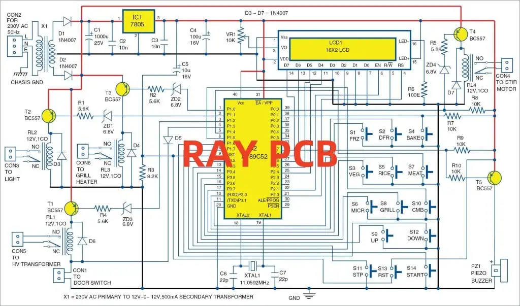
2. Components of Circuit Board Schematics
Circuit board schematics are composed of various symbols and conventions that represent different electrical components and their interconnections. Here are some of the key components:
- Electrical Components: Schematics employ standardized symbols to represent various electrical components, such as resistors, capacitors, integrated circuits (ICs), transistors, and connectors. These symbols provide a clear visual representation of the component’s function and type.
- Interconnections: Lines and wires in schematics represent the electrical connections between components, indicating the flow of current or signals. These interconnections can be labeled with net names or reference designators for clarity.
- Power and Ground Symbols: Schematics include specific symbols to represent power sources (e.g., batteries, voltage regulators) and ground connections, which are essential for proper circuit operation.
- Reference Designators: Each component in a schematic is assigned a unique reference designator, typically a combination of letters and numbers, to facilitate easy identification and cross-referencing with other documentation or the physical PCB layout.
- Annotations and Notes: Schematics may include annotations, notes, or comments to provide additional information or clarification regarding specific components, connections, or design considerations.
3. Schematic Conventions and Standards
To ensure consistency and clarity in circuit board schematics, various conventions and industry standards have been established. Adhering to these standards is crucial for effective communication and collaboration within the electronics industry:
- Schematic Symbols: Organizations like the Institute of Electrical and Electronics Engineers (IEEE) and the International Electrotechnical Commission (IEC) have defined standardized symbols for representing electrical components in schematics. These symbols are widely recognized and used to ensure consistent interpretation.
- Schematic Layouts: Conventions exist for the arrangement and organization of components within schematics, such as grouping related components together or separating different functional blocks for clarity.
- Schematic Hierarchy: Complex circuits may be divided into multiple schematic sheets or hierarchical levels, with each sheet representing a specific functional block or subsystem. Cross-references and interconnection markers provide seamless navigation between these sheets.
- Design Rules and Constraints: Schematics often incorporate design rules and constraints specific to the intended application or manufacturing process, such as voltage or current ratings, component footprint specifications, or clearance requirements.
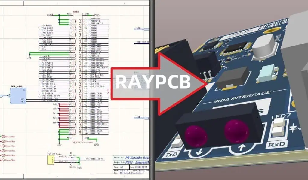
4. Schematic Capture Tools and Software
In today’s modern electronics design workflow, dedicated schematic capture tools and software are widely used to create, edit, and manage circuit board schematics. These tools offer various features and capabilities, including:
- Schematic Entry: Graphical user interfaces (GUIs) and libraries of pre-defined component symbols facilitate efficient schematic entry and circuit design.
- Design Rule Checking (DRC): Built-in DRC functionality helps identify and resolve potential issues or violations in the schematic, ensuring compliance with design rules and constraints.
- Simulation and Analysis: Many schematic capture tools integrate with circuit simulation and analysis tools, allowing designers to verify and optimize circuit behavior before moving to the physical layout stage.
- PCB Layout Integration: Seamless integration with PCB layout tools enables the automatic translation of schematics into physical PCB layouts, streamlining the design process.
- Version Control and Collaboration: Advanced schematic capture tools support version control and collaboration features, enabling multiple designers to work on the same project simultaneously and track changes effectively.
| Component | Description |
|---|---|
| Electrical Components | Standardized symbols representing various electrical components |
| Interconnections | Lines and wires representing electrical connections between components |
| Power and Ground Symbols | Symbols representing power sources and ground connections |
| Reference Designators | Unique identifiers assigned to each component for cross-referencing |
| Annotations and Notes | Additional information or clarification regarding components or design considerations |
FAQs

- Q: Why are circuit board schematics important in the PCB design process? A: Circuit board schematics are crucial in the PCB design process for several reasons: they provide a clear representation of the circuit functionality, enable design verification, serve as comprehensive documentation, and form the foundation for generating the physical PCB layout. Schematics ensure accurate translation from the conceptual design to the final product.
- Q: What are the key components of a circuit board schematic? A: The key components of a circuit board schematic include electrical component symbols, interconnection lines/wires, power and ground symbols, reference designators for components, and annotations or notes for additional information.
- Q: Why is it important to follow schematic conventions and industry standards? A: Adhering to schematic conventions and industry standards is crucial for effective communication and collaboration within the electronics industry. Standardized symbols, layouts, and design rules ensure consistent interpretation and facilitate seamless collaboration among designers, manufacturers, and other stakeholders.
- Q: What are some common features of modern schematic capture tools and software? A: Modern schematic capture tools and software offer features such as graphical user interfaces for efficient schematic entry, design rule checking (DRC) functionality, integration with circuit simulation and analysis tools, seamless integration with PCB layout tools, and version control and collaboration capabilities.
- Q: How do circuit board schematics relate to the physical PCB layout? A: Circuit board schematics serve as the foundation for generating the physical PCB layout. PCB design software tools utilize the schematic information, including component connections and placement, to automatically translate the conceptual design into the physical layout of the PCB, ensuring accuracy and consistency between the schematic and the final product.