Top 10 Printed Circuit Assembly Suppliers in China

pcb assembly cost down

Introduction

China has become the foremost destination for electronics manufacturing services (EMS) globally. A large and ever-expanding network of EMS providers in China offer printed circuit board assembly (PCBA), testing, box build, and other value-added services for OEMs across industries and geographies.

With so many EMS companies to choose from, how do you select the right partner for your PCBA needs in China? In this comprehensive guide, we identify and profile the top 10 printed circuit board assembly suppliers in China based on key criteria like capabilities, capacity, certifications, and customer experience.

How We Identified the Top Printed Circuit Assembly Suppliers in China

We used a data-driven methodology to curate the list of top 10 PCBA suppliers in China:

  • Capability Analysis โ€“ PCBA technology capabilities based on site audits, surveys and direct feedback.
  • Capacity Scalability โ€“ Ability to scale from small lots to high volume production.
  • Geographic Footprint โ€“ Coverage across China with multiple factories.
  • Certifications โ€“ Industry certifications like IATF 16949, AS9100, ISO 13485, ISO 9001.
  • Customer Base โ€“ Diversity of industry verticals served.
  • Customer Feedback โ€“ Direct customer reviews and testimonials.
  • Continuous Improvement โ€“ Investments in new capabilities and productivity.
  • Supply Chain Maturity โ€“ IT systems, quality processes and supply chain infrastructure.

This provides a 360-degree view of the EMS firmโ€™s capabilities for identifying the top PCBA partners.

Top 10 Printed Circuit Assembly Suppliers in China

RayMing-PCB-and-Assembly

Based on the above methodology, here are the top 10 printed circuit board assembly suppliers in China:

1. RayMing Technology

Founded in 2005, RayMing has become a leading EMS provider in China with specialized capabilities tailored for low-to-medium volume, high mix PCBA. With IATF 16949 certification and nearly 500 employees, RayMing operates large manufacturing sites in both Shenzhen and Suzhou.

Core Capabilities:

Industry Focus: Industrial automation, automotive electronics, medical devices.

Customers: Siemens, OSRAM, Caterpillar, Medtronic

Locations: Suzhou, Shenzhen

Certifications: IATF 16949, ISO 13485, ISO 9001

Volume Range: 500 – 50,000 pcs/month

Customer Feedback:

โ€œWe are very satisfied with RayMing’s manufacturing expertise. They delivered high quality boards on schedule, and provided valuable DFM input to optimize our design.โ€ – R&D Director, Fortune 500 Automation Company

2. Benchmark Electronics

Benchmark provides advanced precision electronics manufacturing with over 50 sites across the Americas, Europe, and Asia. Their China facilities located in Suzhou, Shanghai, and Chengdu offer specialized engineering services combined with volume manufacturing.

Core Capabilities:

Industry Focus: A&D, medical, high-performance computing

Customers: Raytheon, BMW, HP, Olympus

Locations: Suzhou, Shanghai, Chengdu

Certifications: ISO13485, ISO 9001, AS9100D

Volume Range: 1,000 – 250,000 pcs/month

Customer Feedback:

โ€œBenchmark delivered very good quality boards on time for our new medical device. We will use them for future programs as well.โ€ โ€“ R&D Manager, Healthcare OEM

3. Compal Electronics

Compal is one of the largest ODMs in Asia, providing design, engineering and manufacturing services for computing, communications and consumer electronics. Their China factories feature high volume SMT and automated assembly combined with ruggedized quality standards.

Core Capabilities:

  • High volume SMT assembly
  • End-of-line packaging
  • Automated manufacturing
  • Inventory management
  • ODM/OEM solutions

Industry Focus: Consumer electronics, computing

Customers: Amazon, Dell, HP, Motorola

Locations: Shanghai, Chongqing, Chengdu

Certifications: TL9000, ISO 9001

Volume Range: 50,000 โ€“ 1,000,000 pcs/month

Customer Feedback:

โ€œWe partnered with Compal for a high volume product ramp. They delivered great quality boards on time to meet our launch schedule.โ€ โ€“ Sourcing Manager, Multinational Software Company

4. Flex

Flex is among the largest global EMS providers with an extensive footprint in China including Shanghai, Zhuhai, and Suzhou. They provide advanced manufacturing solutions combining industry expertise, engineering services, and factory automation.

Core Capabilities:

  • High volume SMT assembly
  • System integration and test solutions
  • Flexible automation concepts
  • Value engineering
  • Supply chain optimization

Industry Focus: Computing, automotive, medical, industrial

Customers: Bosch, Cisco, HP, Johnson & Johnson

Locations: Shanghai, Suzhou, Zhuhai

Certifications: ISO 9001, ISO 13485, AS9100D

Volume Range: 50,000 โ€“ 500,000 pcs/month

Customer Feedback:

โ€œFlex delivered solid PCBA quality and helped optimize our design for manufacturing. Their automation expertise supported our high volume ramp.โ€ โ€“ Operations Director, Networking Hardware Company

5. Pegatron

Pegatron is a leading electronics ODM with design, manufacturing and service capabilities spanning components, computing, communications and consumer electronics. Their China factories are highly automated to produce high volumes with quality and precision.

Core Capabilities:

  • High volume automated SMT
  • System assembly and integration
  • Supply chain management
  • Inventory control systems
  • Manufacturing engineering

Industry Focus: Computing, communication networks, consumer electronics

Customers: Microsoft, Sony, Fitbit, DJI

Locations: Shanghai, Kunshan

Certifications: ISO 9001, ISO 14001, OHSAS 18001

Volume Range: 100,000 โ€“ 5,000,000 pcs/month

Customer Feedback:

โ€œPegatron delivered very good quality and helped achieve our cost targets through their manufacturing engineering expertise.โ€ โ€“ Sourcing Manager, Wearable Devices Company

6. Sanmina Corporation

Sanmina provides electronics manufacturing services across all major continents. Their China facilities located in Suzhou and Chengdu offer advanced engineering along with precision component manufacturing and complex PCBA.

Core Capabilities:

  • Advanced SMT assembly
  • Complete box build services
  • Complex system assembly
  • Supply chain services
  • Component engineering

Industry Focus: Communications, medical, defense, automotive

Customers: Bosch, Philips, Panasonic, Raytheon

Locations: Suzhou, Chengdu

Certifications: ISO 13485, ISO 9001, AS9100D

Volume Range: 10,000 โ€“ 250,000 pcs/month

Customer Feedback:

โ€œSanmina delivered complex PCBAs with solid quality. Their engineers were very responsive throughout the project.โ€ โ€“ Engineering Director, Defense Contractor

7. Season Group

Season Group is an EMS provider with factories in China, Hong Kong and Mexico. Their China facilities located in Dongguan and Huizhou offer advanced manufacturing capabilities tailored for medical, industrial and specialty electronics markets.

Core Capabilities:

  • Complex PCBA down to 01005 components
  • Fine pitch component assembly
  • Prototyping and NPI
  • Full box build and packaging
  • Conformal coating

Industry Focus: Medical devices, industrial controls, robotics

Customers: Medtronic, Abbott, Emerson

Locations: Dongguan, Huizhou

Certifications: ISO 13485, ISO 9001

Volume Range: 1,000 โ€“ 150,000 pcs/month

Customer Feedback:

โ€œSeason Group delivered PCBA prototypes quickly. Their attention to quality will make them a long-term partner.โ€ โ€“ Engineering VP, Medical Devices Startup

8. Jabil Circuit

Jabil provides comprehensive electronics design, manufacturing and product management globally. Their China manufacturing locations offer specialized expertise tailored for major end markets including networking, communications, automotive and healthcare.

Core Capabilities:

  • High precision SMT assembly
  • Automated wave and selective soldering
  • High quality conformal coating
  • Press-fit manufacturing
  • Functional test solutions

Industry Focus: Data networking, telecom infrastructure, automotive, healthcare

Customers: Cisco, Johnson & Johnson, Ford, Renault

Locations: Guangzhou, Xiamen, Shenzhen

Certifications: IATF 16949, ISO 13485, TL 9000

Volume Range: 10,000 โ€“ 500,000 pcs/month

Customer Feedback:

โ€œJabil delivered solid quality boards on schedule. Their manufacturing expertise in press-fit connectors was valuable.โ€ โ€“ Operations Director, Data Communications Company

9. New Kinpo Group

New Kinpo Group provides end-to-end manufacturing services spanning components, modules, system assembly, distribution and after-sales support. Their China factories are located in Shanghai, Kunshan and Shenzhen.

Core Capabilities:

  • High precision SMT assembly
  • Automated volume manufacturing
  • Supply chain optimization
  • Manufacturing engineering
  • Inventory management

Industry Focus: Computing, networking, consumer electronics, automotive

Customers: Microsoft, Google, Amazon, Continental

Locations: Shanghai, Kunshan, Shenzhen

Certifications: ISO 9001, ISO 14001, TL 9000

Volume Range: 50,000 โ€“ 1,000,000 pcs/month

Customer Feedback:

โ€œNew Kinpoโ€™s PCBA quality was very good. Their optimization of our bill of materials helped reduce costs.โ€ โ€“ Sourcing Director, Tech Company

10. Zollner Elektronik AG

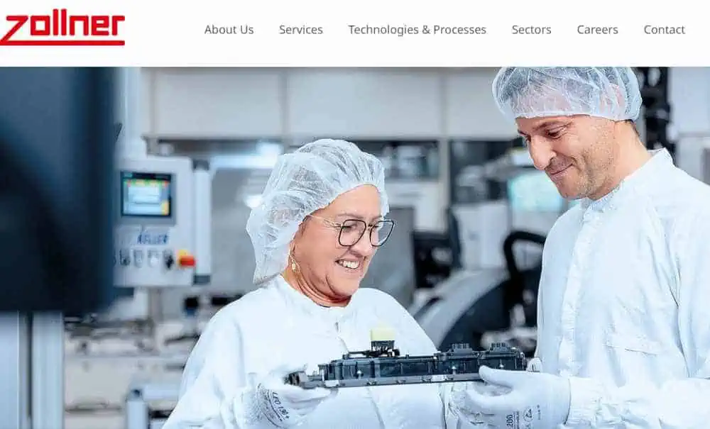
Zollner provides full system design-to-manufacturing services spanning mechanical, electrical and electronic solutions. Their facility in Taicang, China provides specialized expertise in high mix, low-medium volume PCBA manufacturing.

Core Capabilities:

  • Flexible SMT assembly down to 01005 components
  • Selective, wave and automated optical soldering
  • Press-fit manufacturing
  • Full box-build assembly
  • Functional test solutions

Industry Focus: Industrial automation, automotive, medical devices

Customers: Osram, Hella, SMA Solar

Location: Taicang

Certifications: ISO 9001, ISO 14001, ISO 13485

Volume Range: 500 โ€“ 50,000 pcs/month

Customer Feedback:

โ€œZollner delivered prototype and low volume production PCBA orders with high quality results.โ€ โ€“ Engineering Manager, Automation Components Company

How to Select the Right PCBA Supplier in China

Here are some key selection criteria OEMs should consider when choosing a PCBA partner in China:

  • Technical capabilities โ€“ Assess the supplierโ€™s expertise related to your specific product needs like fine pitch assembly, selective soldering, coating.
  • Industry experience โ€“ Suppliers focused on key verticals often provide more relevant guidance and solutions.
  • Production capacity โ€“ Ensure adequate capacity for current volumes and scalability for future growth.
  • Quality certifications โ€“ Look for certifications like IATF 16949, ISO 13485 which validate process maturity.
  • Customer references โ€“ Ask for references and success cases from customers in similar industries.
  • Site visits โ€“ Auditing the facility validates capabilities and gives deeper insights into process maturity.
  • Engineering support โ€“ Evaluate the depth of manufacturing engineering skills for optimization and problem solving.
  • Supply chain infrastructure โ€“ Mature ERP and warehouse systems ensure part availability and program transparency.
  • Continual improvement โ€“ Research investments in new capabilities, employee training, quality initiatives.
  • Cost competitiveness โ€“ Compare fully landed costs between suppliers considering value-added services.

By balancing these aspects, OEMs can identify the right PCBA partner matching their unique product needs and business goals in the expansive electronics manufacturing ecosystem in China.

Conclusion

China offers the most extensive EMS infrastructure globally, with a large and ever-growing base of competent PCBA service providers. Identifying the right partner goes beyond searching manufacturing capabilities – it requires aligning values and building trusted strategic relationships. We hope this guide to the top 10 PCB assembly companies in China provides insights into the country’s manufacturing excellence and helps you find the best match for your program needs.

Frequently Asked Questions

Q1. Which city has the most PCB assembly suppliers in China?

The largest concentration of PCBA providers in China is centered in the Greater Shanghai area including Suzhou, Kunshan and Shanghai. Other major EMS hubs are in Shenzhen and Chengdu.

Q2. What volume production can PCB assembly suppliers in China handle?

Leading PCBA suppliers in China can handle volumes ranging from a few hundred boards for prototyping to over 1 million boards per month in high volume production.

Q3. Does China PCBA quality match international standards?

Yes, China PCBA quality from mature EMS suppliers matches world-class standards. Many have certifications like IATF 16949, ISO 13485, AS9100 demonstrating process maturity.

Q4. Can China PCBA suppliers scale with product volumes?

Established PCBA suppliers have expertise in scaling production volumes smoothly from prototypes to high volume ramps through process refinement and capacity expansion.

Q5. How long does shipping take from China to the US?

Average shipping times by air freight from China to the US are 5-7 days. Sea shipments take 3-4 weeks on average. Expedited shipping can be as fast as 3-4 days.

4 layer Flex PCB Manufacturing and Stackup guidelines

4 layer flex pcb board
4 layer flex pcb

4 layer flex PCB are used in a variety of industrial applications. Our flex PCBs are first choice for industries such as power, automobile, medical devices, GPS, and industrial control equipment, to name a few.

Four Layer Flex PCB Stack up

4 layer flexible PCB

Introduction

Flexible printed circuits (FPCs) provide invaluable dynamic flexing and shape conforming capabilities in electronics. 4 layer flex PCBs with conductors on 4 layers enable increased routing density and integration versus 2 layer flex, while retaining excellent flexibility.

This article examines 4 layer flex stackup configurations, critical design guidelines, the manufacturing challenges involved, advanced capabilities needed for quality 4 layer FPCs, and techniques for optimizing performance.

What is a 4 Layer Flex PCB?

A 4 layer flex PCB consists of:

  • Flexible base dielectric material such as polyimide forming the core.
  • Copper foil conductors patterned on the top, bottom and two inner layers of the core.
  • Cover layers laminated above and below for insulation, abrasion resistance and stiffness.
  • Plated through holes (PTH) and buried vias for vertical interconnections.
  • Edge contacts or stiffeners to provide external connections.

This construction provides the highest routing density on a flex PCB with fine conductors and clearances.

Applications of 4 Layer Flex Circuits

Some common applications leveraging 4 layer flex PCB technology include:

  • Wearable devices โ€“ Smart watches, fitness trackers, AR/VR headsets.
  • Flexible displays โ€“ Edge or foldable displays, large LED video walls.
  • Automotive โ€“ In-car displays, lane departure systems, LiDAR.
  • Aerospace/Military โ€“ Helmet systems, communications, guidance systems.
  • Medical โ€“ Ultrasound transducers, implants, endoscopes.
  • Industrial โ€“ Flexible HMIs, robotic interconnects, motion control.
  • Consumer Electronics โ€“ Foldable phones, cameras, portable electronics.

The ultra-dense interconnect capabilities of 4 layer FPCs supports the complex, compact and lightweight requirements of these applications.

Benefits of 4 Layer Flexible PCBs

Some key advantages of 4 layer flex PCBs are:

  • Maximum routing density โ€“ Complex, compact layouts with traces on 4 layers.
  • Embedded discrete passives โ€“ Buried resistor, capacitor and inductor integration.
  • Controlled impedances โ€“ Tight impedance control for matched high speed signals.
  • Integrated shielding โ€“ Entire layers can provide EMI/RFI isolation.
  • Higher component density โ€“ More components in a given area with multilayer escape routing.
  • Multilayer stacking โ€“ Can integrate other flex or rigid-flex layers.
  • Greater functionality โ€“ High density interconnects enable more capabilities and features.
  • Miniaturization โ€“ Ideal for complex circuits in small, lightweight products.
  • Lower assembly costs โ€“ Eliminates separate flexible cabling and connectors.
  • High frequency performance โ€“ Controlled impedances benefit RF applications.

4 Layer Flex PCB Stackup Configurations

Common 4 layer flex stackup arrangements include:

Symmetrical Arrangement

Coverlayer Signal Layer 1
Ground Plane Signal Layer 2 Flexible Core Dielectric Signal Layer 3 Ground Plane Signal Layer 4 Coverlayer

This offers good EMI control with ground plane shielding and similar layer structures on both sides of the core.

Asymmetrical Arrangement

Coverlayer Signal Layer 1 Ground Plane 1 Power Layer
Flexible Core Dielectric Signal Layer 2 Ground Plane 2 Signal Layer 3 Coverlayer

Here power and ground planes are distributed on each side of the core dielectric to provide isolation between signals.

High Speed Arrangement

Coverlayer Signal Layer 1 Ground Plane 1 Signal Layer 2 Flexible Core Dielectric Signal Layer 3 Signal Layer 4 Ground Plane 2 Coverlayer

Fast signals demanding impedance control are assigned to the outer layers in this configuration. Power and ground planes provide constant reference planes.

Challenges in 4 Layer Flex PCB Fabrication

While delivering substantial benefits, producing 4 layer flex PCBs poses difficulties:

  • Achieving fine lines and spaces on multiple flexible layers.
  • Holding tight layer-to-layer registration through all photolithography stages.
  • Producing high density of buried and blind microvias with thin dielectric.
  • Preventing lifted lands or cracked barrel plating on PTHs during flexing.
  • Maintaining reliable coverlayer and stiffener adhesion through dynamic flexing.
  • Controlling characteristic impedances across multiple flex layers.
  • Managing thermomechanical stresses and fatigue prone areas.
  • Qualification testing of impedance shifts under long term flex cycling.
  • Ensuring flex fold and bend cycle life reaches millions of cycles.

Advanced Manufacturing Capabilities Required

Flexible Printed Circuit Board Manufacturers

To reliably fabricate 4 layer flex circuits, PCB manufacturers need substantial expertise:

  • Fine line etching โ€“ Trace/space widths down to 25ฮผm on multilayer flex materials.
  • Registration accuracy โ€“ Alignment of +/- 50ฮผm between flexible layers.
  • Microvia construction โ€“ Laser drilled and plated blind/buried vias with 1:1 capture pads.
  • ANNULAR ring control โ€“ Producing 1 mil rings reliably on buried microvias.
  • Multilayer bonding โ€“ Interlayer peel strength over 2.5N/mm without delamination.
  • Surface finish โ€“ Immersion silver with thickness uniformity of <10% across flex contours.
  • Impedance tolerance โ€“ Tight impedance control within 5% of target value.
  • Flexible solder mask โ€“ Liquid photoimageable (LPI) solder mask optimized for flexing.
  • Reliability testing โ€“ Extreme temperature cycling, twisting, bending, vibration and drop testing.
  • Process Control โ€“ Real-time statistical process monitoring and control.
  • Flex fold engineering โ€“ Precisely defined and characterized bend radiuses backed by extensive test data.

4 Layer Flex Design Recommendations

Some key guidelines when designing 4 layer flex PCBs:

  • Plan stackup arrangement to isolate critical signals using ground planes.
  • Use impedance matched traces with adequate shielding for high speed signals.
  • Model impedances and performance under dynamic bending conditions.
  • Widen trace/space dimensions in flexing areas relative to rigid sections.
  • Incorporate strain relief structures at interfaces between rigid and flex sections.
  • Utilize thermal reliefs for solder joints to reduce stresses.
  • Add stiffeners or covers for rigidity at connection points.
  • Maximize distance of components from high flex zones.
  • Define and specify multiple controlled bend radii rather than arbitrary flexing.
  • Review layouts for susceptibility to acid traps during fabrication.
  • Specify microvia capture pads with 1:1 aspect ratio for reliability.
  • Consider needs for shielding, insulation and abrasion resistance in stackup design.

Conclusion

4 layer flex PCB technology enables innovative products with maximum routing density combined with dynamic flexing capabilities. To harness these benefits requires proper stackup configurations, controlled processes, and sound flex design techniques. Partnering with an expert flex PCB manufacturer having robust 4 layer technology maturity allows designers to fully leverage the advantages of 4 layer flex to develop cutting-edge solutions for flex electronics integration needs across industries.

2 layer flex pcb stackup and Manufacturing

2 layer flex pcb board
double sided flex PCB

Double-Sided Flexible PCB : Double-sided flex PCB feature two conductive layers with a layer of polyimide insulation between them. The conductive layerโ€™s outer sides can be either exposed or have covers, like a copper pad. Layers are connected typically by plated through-holes, but other methods can be used. Like the single-sided flexible circuits, the double-sided flexible PCB can support additional elements such as pins, connectors and stiffeners.

Double Sided Flexible PCB Stack Up

Double Sided Flexible PCB

Introduction

Flexible printed circuits (FPCs) enable unique capabilities like dynamic flexing and conforming to surfaces which are not possible with rigid boards. 2 layer flex PCBs with conductors patterned on both sides of a dielectric offer more interconnect density versus single sided flex, while retaining excellent flexibility.

This article examines 2 layer flex stackup configurations, critical design considerations, the manufacturing challenges involved, advanced capabilities needed for quality 2 layer FPCs, and guidelines for optimizing performance.

What is a 2 Layer Flex PCB?

flexible circuit board

A 2 layer flex PCB consists of:

  • Flexible base dielectric material such as polyimide. This forms the core.
  • Copper foil conductors patterned on both sides of the base material.
  • Cover layers laminated over the etched traces for insulation, abrasion resistance and stiffness.
  • Plated through holes (PTHs) for interconnecting between conductors on each side.
  • Edge contacts or stiffeners to provide external connections.

The 2 metal layers bonded to a thin, flexible core dielectric provide a robust flex circuit construction with enhanced interconnect density versus single sided FPCs.

Applications of 2 Layer Flex Circuits

Some common applications of 2 layer flex PCB technology include:

  • Displays โ€“ Flexible OLED displays, curved touch sensors.
  • Automotive โ€“ Seat control panels, steering wheel electronics.
  • Consumer Electronics โ€“ Foldable phones, wearables, VR headsets.
  • Medical โ€“ Catheters, implants, transdermal patches.
  • Robotics โ€“ Flexible cabling for manipulator joints.
  • Defense/Military โ€“ Rugged flexible electronics, avionics systems.
  • Industrial – Flexible sensors, actuators, kontrollers.

The compactness, dynamic flexing and extended cycle life of 2 layer FPCs make them well suited for these applications.

Benefits of 2 Layer Flex PCBs

Some key advantages of 2 layer flex PCBs are:

  • Double routing density โ€“ Traces and componenets on both sides doubles layout area.
  • Integrated shielding โ€“ Ground planes can shield signals from EMI/RFI.
  • Embedded components โ€“ Passives can be embedded within flex layers.
  • Impedance control โ€“ Better impedance matching with sandwiched microstrips.
  • Higher interconnection density โ€“ More interconnects with fine traces on two sides.
  • Rigid sections โ€“ Can incorporate stiffened sections for component mounts.
  • Smaller product size โ€“ High density flex packing enables miniaturization.
  • Lower assembly cost โ€“ Fewer discrete wires and connectors to assemble.
  • Three-dimensional – Dynamic shaping and folding around structures.
  • High frequencies โ€“ Controlled impedances benefit high frequency performance.

2 Layer Flex PCB Stackup Configurations

Typical stackup structures used in 2 layer flex PCBs include:

Coverlayer Based Stackup

Coverlayer 1
Signal Layer 1 Flexible Core Dielectric Signal Layer 2 Coverlayer 2

This offers good abrasion resistance and insulation with coverlayers enveloping the conductors.

Adhesive Based Stackup

Signal Layer 1 Bonding Adhesive Flexible Core Dielectric Bonding Adhesive Signal Layer 2

Here the core dielectric is sandwiched between conductors using adhesive bonding films. Provides ultra-thin profile.

Copper Clad Stackup

Signal Layer 1 Flexible Core Conductor Signal Layer 2

In this case, the flexible copper clad dielectric itself functions as the core, removing the need for bonding. Can be cost-effective.

Shielded Stackup

Coverlayer 1 Signal Layer 1 Flexible Core Dielectric Ground Plane 2 Signal Layer 2 Coverlayer 2

The embedded ground plane provides shielding between signals and blocks EMI.

Challenges in 2 Layer Flex PCB Manufacturing

While providing many benefits, fabricating 2 layer flex PCBs poses manufacturing difficulties including:

  • Achieving and maintaining fine line resolution on both sides.
  • Tight layer-to-layer registration across two flexible sides.
  • Preventing delamination or separation between layers.
  • Producing plated through holes with adequate annular rings.
  • Controlling impedances across dynamically flexing layers.
  • Avoiding rigid sections from detaching on flexing.
  • Managing thermomechanical stresses from flexing.
  • Maintaining solder joint integrity across flex cycles.
  • Handling, processing and assembling extremely thin circuits.
  • Ensuring flexibility and performance with embedded passives.
  • Qualifying and modeling impedance shifts under various flex configurations.

Advanced Manufacturing Capabilities Needed

semi-flex-pcb

High quality 2 layer FPC production requires manufacturers to demonstrate several advanced capabilities:

  • Fine line etching – Trace/space down to 25ฮผm on thin flex cores reliably.
  • Registration accuracy โ€“ Alignment around 50 to 75ฮผm between flex layers.
  • Annular ring control โ€“ Producing 1 mil annular rings on small PTHs.
  • Flexible solder masks โ€“ Halogen-free liquid photoimageable (LPI) masks.
  • Reliable multilayer bonding – Interlayer peel strengths above 2 N/mm without delamination.
  • Surface finish – Uniform plating thickness of immersion Ag or Sn across dynamic contours.
  • Fine space via tenting – Protecting ultra-fine trace gaps during PTH drilling.
  • Flex fold engineering โ€“ Highly controlled folding with extensive test data.
  • Plated through holes โ€“ Smooth, void free copper plating of PTHs with 1:1 aspect ratio.
  • Process control โ€“ Real-time Statistical Process Control (SPC) for stability.

Reliability testing – Dynamic bend cycling, twist, vibration, thermal shock, drop testing.

2 Layer Flex PCB Design Considerations

Some key design aspects when working with 2 layer flex circuits include:

  • Modeling electrical performance under different bend configurations and cycles.
  • Assigning critical signals requiring impedance control or low skew to outer layers.
  • Using wider traces than rigid PCBs and allowing adequate spacing between traces.
  • Adding shielding planes or ground fills if EMI is a concern.
  • Using linear routing for traces along the bend axis and minimizing perpendicular traces.
  • Watching for impedance variations at transitions between rigid and flex sections.
  • Accounting for registration shifts between layers during dynamic flexing.
  • Providing sufficient annular ring margins around plated through holes.
  • Ensuring vias have 1:1 capture pad aspect ratios for reliability.
  • Incorporating thermal reliefs to reduce thermomechanical solder joint stresses.
  • Adding EMI shielding vias around components if needed.
  • Utilizing stiffeners, encapsulation and strain relief structures at stress points.

Conclusion

2 layer flexible PCBs enable increased routing density and the ability to integrate shielding planes while retaining excellent dynamic flexing capabilities. Harnessing these benefits requires mature flex PCB manufacturing processes and disciplined design techniques tailored for flex. When designed properly, robust 2 layer flex circuits provide electronics engineers an invaluable technology for developing innovative, compact and motion-tolerant products.

What is Single Sided Flexible PCB?

one layer flex pcb board

Single Sided Flexible PCB 

Single sided Flex PCB

single sided Flex PCB are the most basic type of flexible circuits. They consist of a flexible dielectric film laminated to a single sheet of copper. The copper layer is then chemically etched according to the specified circuit pattern design. Polyimide cover lays can be added to the circuit board for additional insulation and protection, if desired.

single side Flexible PCB Stack up

Single-Sided Flexible PCB : This design includes a single conductive copper layer that can   be bonded between two layers of insulation or built with one polyimide insulating layer and an uncovered side. The interior copper layer then goes through a chemical etching process, producing the circuit design. Single-sided flex PCB board designs support the inclusion of electronic components, connectors, pins and stiffeners.

Learn more about:

Introduction

Printed circuit boards (PCBs) provide the interconnect foundation in electronics products. While rigid boards are most common, flexible PCBs (FPCBs) offer unique advantages for applications requiring dynamic flexing, bending or shaping around structures. Single sided flex circuits with conductors only on one side are the simplest FPCB construction.

This article will examine what single sided flexible PCBs are, their typical applications and benefits, materials and construction methods used, critical manufacturing capabilities needed, and key design considerations when implementing single sided flex circuits.

What is a Single Sided Flex PCB?

flex pcb capability

A single sided flexible PCB consists of:

  • A flexible dielectric base made of polyimide or other flexible polymer substrates.
  • Conductive copper traces etched on one side of the base material.
  • No conductors or dielectric on the reverse side.

This provides a thin, lightweight and highly bendable circuit layer with traces on only one side. Connections to the conducting layer are made using:

  • Plated through holes (PTHs) drilled through the base substrate.
  • Edge contacts formed along one or more edges of the circuit.
  • Metal stiffeners or connectors soldered to pads on the flex layer.

Applications of Single Sided Flex Circuits

Some common applications of single sided flex PCB technology include:

  • Wearable devices โ€“ Fitness trackers, smart watches, health monitoring devices.
  • Displays โ€“ Flexible displays, electronic signage and indicators.
  • Medical – Catheters, implants, transdermal patches.
  • Automotive โ€“ Seat heaters, capacitive switches, sensors.
  • Consumer Electronics โ€“ E-readers, headphones, VR headsets.
  • Robotics โ€“ Flexible cabling for joints and manipulators.
  • IoT devices – Flexible sensor nodes and connectors.

The dynamic flexing and continuous motion capabilities of single sided FPCBs suit them for these applications.

Benefits of Single Sided Flexible PCBs

Some key benefits of single sided flex circuits versus rigid boards are:

Dynamic Flexing – Can withstand extensive flexing and shape change required in motion applications.

Lightweight – Weigh 60-80% less than equivalent rigid boards.

Thin profile โ€“ As thin as 25ฮผm flex layers permit tight installations and stacking.

High density โ€“ Finer lines/spaces allow dense interconnections in small areas.

Three-dimensional โ€“ Can bend and conform to 3D surface shapes.

Embedded passivesCapacitors and resistors can be screened for compactness.

Low cost โ€“ Eliminates components, connectors and simplifies assembly.

High frequency โ€“ Controlled impedances and unattenuated signals at high frequencies.

Durability โ€“ Polyimide materials withstand millions of flex cycles.

Aesthetics – Can produce stylish, low profile products.

Single Sided Flex PCB Materials

Typical materials used to fabricate single sided flex PCBs include:

Base Dielectric – Polyimide is most common. Can also use LCP, PEN, PET, PU. Polyimide provides the highest flexibility and temperature durability.

Conductor – Electrodeposited copper foil, typically 12-35ฮผm thickness. Rolled annealed copper offers optimal flexure performance.

Bonding Adhesive – Acrylic or epoxy based adhesive films attach stiffeners, connectors or components.

Cover layer – Optional polyimide or adhesive covers can be added for insulation or stiffness.

Stiffeners – Selective FR4 stiffeners may be added in flex areas requiring rigid mounting surfaces.

Finishes – Immersion tin or silver over nickel are typically used for solderability and durability.

Critical Manufacturing Capabilities

Single-sided Flex PCB

Producing robust, reliable single sided flex PCBs requires advanced manufacturing expertise:

  • Fine line etching – Ability to reliably produce and hold trace widths/spaces down to 50ฮผm.
  • Registration accuracy – Tight process control to meet registration tolerances around 50-75ฮผm .
  • Surface finish uniformity – Consistent immersion silver or tin plating thickness across flex circuits.
  • Quality laminating – Eliminating delamination or separation failures through process controls.
  • Flex fold engineering – Highly controlled folding based on extensive modeling and testing data.
  • Conductor adhesion – Adhesion strength of copper traces exceeding 1.5N/mm on polyimide.
  • Plated through holes – Smooth, void free copper plating of small through holes.
  • Panel handling – Special carriers, tooling and protocols to avoid damage to flex layers.
  • Reliability testing – Environmental testing, dynamic flex cycling, vibration and shock exposure.

Process control – Statistical control and continuous improvement for process stability.

Single Sided Flex PCB Design Considerations

Key design aspects when implementing single sided flex boards include:

  • Trace widths and spacing โ€“ Use wider traces than rigid boards as narrow traces may break on flexing. Space traces adequately apart for flexibility.
  • Trace routing โ€“ Route traces linearly in the direction of bending rather than perpendicular to the flex axis. Avoid sharp turns.
  • Bend areas โ€“ Use fewer traces in sections that undergo maximum bending. Add stiffeners if needed.
  • Bond pad openings โ€“ Allow for adequate bonding material around component pads for shear strength.
  • Annular rings โ€“ Maintain sufficient annular rings around plated through holes for adhesion.
  • Fold compensation โ€“ Account for swelling of outer side and shrinkage of inner side when folded.
  • Adhesives โ€“ Select flexible adhesives optimized for flexing rather than rigid bonds.
  • Reinforcements โ€“ Add stiffeners and backing structures selectively in high stress areas.
  • Termination โ€“ Use robust, flexible solderable edge connector contacts.
  • Impedances โ€“ Model electrical performance under various flex configurations.

Conclusion

With their unmatched dynamic flexing capabilities, light weight and thin profile, single sided flexible PCBs enable many new innovative applications not possible with rigid boards. When implementing single sided flex circuits, working with an expert manufacturer and following sound design practices allows harnessing the unique benefits of flex PCBs successfully. As electronics strive for greater motion tolerance, flexibility and structural integration, single sided flex PCB technology provides an enabling interconnect platform.

What is 0.6mm Thickness PCB?

0.6mm pcb thickness
0.6mm pcb

0.6mm PCB is middle thickness of printed circuit board,For double sided PCB is normal,Now more 4 layer and 6 layer PCB use 0.6mm thickness to fix smaller and thinner electronic device .

The laminate thickness as per your specifications and needs. Though, our team offers a standard thickness of 1.6 mm (0.063 inch). Sometimes, the circuit board core thickness and soldermask coating must be considered for trace impedance. When computing impedance, the consequences of conformal coating must be taken into account as the circuit boards are usually covered in soldermask. In general, soldermask decreases the impedance on thin traces. The soldermask has considerably less effect when the trace thickness increases.0.6mm pcb is common for our production, We did 4 layer 0.6mm PCB, 6 layer 0.6mm PCB, and 0.8mm PCB manufacturing.

Circuit board finish differs in rates, availability, serviceable life, consistency and assembly processing. As each finish has its individual advantages, product, the procedures, or setting will define the appropriate surface finish that is suitable for the application. We recommend our users and the designer to constantly coordinate with us for selection of ideal finish for the required product design. This will ensure you have better prices for the end product delivery.

Introduction

Printed circuit boards (PCBs) provide the foundation for mounting and interconnecting electronic components in products. PCB thickness is an important design parameter that affects weight, stiffness, manufacturability and cost. With the trend towards miniaturization in electronics, thinner PCBs around 0.6mm are increasingly being used in dense and compact designs.

This article will examine what 0.6mm PCB thickness means, the manufacturing capabilities needed, key applications for 0.6mm boards, their benefits versus standard 1.6mm PCBs, optimal stackup configurations, and design considerations when using 0.6mm PCB technology.

What Does 0.6mm Thickness Mean?

The thickness of a PCB refers to the total height of the finished multilayer board assembly including conductors, insulating dielectric material and plating finishes. Some standard PCB thickness classes are:

  • 1.6mm – Standard thickness
  • 1.0mm – Typical thinner PCB
  • 0.8mm – Mid-range thin PCB
  • 0.6mm – Ultra-thin PCB
  • 0.4mm – Extremely thin PCB

So a 0.6mm thickness PCB has an overall board height of 0.6mm. This is achieved by using thinner dielectric core and prepreg laminate materials during multilayer PCB fabrication. The thinner laminates enable reducing weight by over 60% compared to standard 1.6mm boards.

Why Use Thinner 0.6mm PCBs?

The key drivers for adopting thinner 0.6mm PCB technology are:

  • Reduce product weight and size for portability
  • Allow greater component density with thinner dielectrics
  • Enable tighter spacing and gap control for denser routing
  • Match thickness with thinner flex-rigid sections in a design
  • Allow additional layers within constrained height envelopes
  • Facilitate integration in thin packages like laptops and tablets
  • Lower material content for cost reduction

For space and weight constrained products, 0.6mm PCBs help achieve miniaturization, portability and integration goals while providing maximum functionality.

Typical Applications of 0.6mm PCBs

Some examples of products that typically utilize 0.6mm thin PCB technology are:

  • Smartphones and tablets
  • Wearable devices
  • IoT endpoints
  • Drones
  • Robotics
  • Laptops
  • Biomedical devices
  • Automotive sensors

The compact, lightweight nature of these applications makes 0.6mm PCBs suitable to facilitate greater densification and packaging flexibility with reduced thickness and mass.

Fabrication Challenges with 0.6mm Boards

rogers substrate

While providing advantages, reliably manufacturing 0.6mm multilayer PCBs poses some fabrication difficulties including:

  • Maintaining registration across multiple thin laminates
  • Achieving high peel strengths between thin cores
  • Preventing resin starvation during lamination
  • Controlling line width and spacing on thin substrates
  • Producing robust multilayer 0.6mm board stackups
  • Minimizing handling damage of flexible thin cores
  • Keeping thin panels stable and warp-free post-etching
  • Achieving desired impedance tolerances

These issues require stringent process control capabilities from the PCB manufacturer.

Key Manufacturing Capabilities for 0.6mm PCBs

To reliably produce 0.6mm multilayer PCBs, manufacturers need to demonstrate several critical capabilities:

  • Registration accuracy – +/- 0.075mm or better registration control.
  • Lamination – Expertise in bonding thin cores using high fillers to avoid voids.
  • Etching – Ability to hold 2 mil lines and spaces on 0.6mm cores.
  • Plating adhesion – Copper bond strength over 4.5N on 0.6mm dielectric.
  • Surface finish – Uniform electrolytic plating thickness across thin panels.
  • Handling – Special carriers and automation to avoid scratches, dents.
  • Stackup design – Modeling and engineering optimal 0.6mm layer configurations.
  • Flatness control – Warp/twist containment through prepreg intervals and balancing.
  • Impedance tolerance – Tight impedance matching within 5% of target.
  • Reliability testing – Thermal shock, temperature cycling, drop/shock testing.

Benefits of 0.6mm vs Standard 1.6mm PCBs

Here is a comparison between typical 0.6mm and standard 1.6mm PCB characteristics:

Parameter0.6mm PCB1.6mm PCB
Thickness0.6mm1.6mm
WeightLower by ~60%Higher
LayersTypically 4-8Typically 2-6
Line Width2 mil capable3 mil typical
Dielectric ConstantConsistentMore variation
Impedance ToleranceTighterLarger tolerances
FlexibilityFlexibleRigid
HandlingNeeds careful handlingEasily handled
Routing DensityHigher, finer featuresLower, larger features
Thermal IssuesLess heat spreadingBetter thermal conduction
ManufacturingTighter process control neededLarger process margins

Optimized Stackup for 0.6mm PCBs

Rogers TC600 PCB

To achieve a robust, reliable 0.6mm board stackup, considerations include:

  • Use thinner dielectrics like 0.2mm or 0.3mm prepregs to conserve total thickness.
  • Incorporate microvias to transition between layers, avoiding through hole vias.
  • Include power and ground planes adjacent to signal layers for isolation.
  • Watch out for impedance discontinuities at layer transitions.
  • Model key signals in PCB analysis tools to shape stackup.
  • Alternate plane directions to balance stresses and avoid warping.
  • Limit asymmetric compositions which produce curl/twist.
  • Allow extra thickness for surface finishes like ENIG or immersion silver.
  • Increase metal core layers if stiffness must be enhanced.
  • Add stiffeners or metal backers selectively if needed.

Design Considerations for 0.6mm PCBs

To effectively leverage 0.6mm boards, engineers should factor in:

  • Accounting for flexibility and handling issues in assembly processes.
  • Minimizing mechanical stresses on the thin boards in the product enclosure.
  • Watching for impedance discontinuities and reflections at layer transitions.
  • Isolating or shielding any sensitive high-speed signals on inner layers.
  • Including thermal relief connections for surface mount parts prone to heating.
  • Measuring temperature rises during operation to avoid hot spots.
  • Reviewing component layouts and spacings for optimal thermal performance.
  • Adding selective stiffening elements if board flexing causes issues.
  • Allowing for higher layer counts within given product height constraints.

Conclusion

With increasing demands for lightweight and thinner products, 0.6mm PCB technology enables reduced mass and size while packing in electronics functionality through greater routing density and layer counts. But achieving robust 0.6mm boards requires advanced manufacturing expertise. With an optimized stackup design and accounting for the unique thermal/mechanical considerations, 0.6mm PCBs can provide a platform for cutting-edge compact product development.

12 Layer PCB Manufacturing and Stack Up Options

12 layer pcb circuit board

12 LAYER PCB Stack Up

Top Layer  โ€ 18um Copper Foil (plated to 35um+)
Preโ€Preg   โ€ 1 x 2116
Layer 2 & 3  โ€ 0.13mm Frโ€4 Core with 35um/35um Copper
Preโ€Preg   โ€ 1 x 2116
Layer 4 & 5  โ€ 0.13mm Frโ€4 Core with 35um/35um Copper
Preโ€Preg   โ€ 1 x 2116
Layer 6 & 7  โ€ 0.13mm Frโ€4 Core with 35um/35um Copper
Preโ€Preg   โ€ 1 x 2116
Layer 8 & 9  โ€ 0.13mm Frโ€4 Core with 35um/35um Copper
Preโ€Preg   โ€ 1 x 2116
Layer 10 & 11  โ€ 0.13mm Frโ€4 Core with 35um/35um Copper
Preโ€Preg   โ€ 1 x 2116
Bottom Layer   โ€ 18um Copper Foil (plated to 35um+)
Stardand 12 Layer PCB  1.6mm +/โ€ 10%

12-Layer <a href="https://www.raypcb.com/how-to-plan-multilayer-pcb-stackup/">PCB Stackup</a> Selector

12-Layer PCB Stackup Selector 12L

Configure layer thicknesses for complex 12-layer HDI and high-speed PCB designs

Quick Presets

Layer Assignment (SIG-GND-SIG-PWR Pattern)
L1 SIG
L2 GND
L3 SIG
L4 PWR
L5 SIG
L6 GND
L7 PWR
L8 SIG
L9 GND
L10 SIG
L11 PWR
L12 SIG

Copper Layers (12)

Prepreg Layers (6)

Core Layers (5)

Total Board Thickness
2.000mm
2000 ยตm
vs 2.0mm
+0 ยตm
Copper (12L)
420 ยตm
Prepreg (6L)
826 ยตm
Core (5L)
800 ยตm

Stackup Visualization

L1 – Top SignalSIG 35ยตm
PP1 114ยตm
L2 – GND PlaneGND 35ยตm
Core 1 100ยตm
L3 – SignalSIG 35ยตm
PP2 114ยตm
L4 – PWR PlanePWR 35ยตm
Core 2 200ยตm
L5 – SignalSIG 35ยตm
PP3 185ยตm
L6 – GND PlaneGND 35ยตm
Core 3 (Center) 200ยตm
L7 – PWR PlanePWR 35ยตm
PP4 185ยตm
L8 – SignalSIG 35ยตm
Core 4 200ยตm
L9 – GND PlaneGND 35ยตm
PP5 114ยตm
L10 – SignalSIG 35ยตm
Core 5 100ยตm
L11 – PWR PlanePWR 35ยตm
PP6 114ยตm
L12 – Bottom SignalSIG 35ยตm
SOLDER MASK (BOTTOM)
Outer Signal
Inner Signal
GND Plane
PWR Plane
Prepreg
Core
๐Ÿ’ก Common 12-Layer Targets
1.6mm: High-density HDI designs
2.0mm: Standard 12L (most common)
2.4mm: Server, networking
3.0-3.2mm: Backplanes, heavy copper
๐Ÿ“ Impedance Zones
Microstrip: L1โ†’L2, L12โ†’L11
Stripline: L3, L5, L8, L10
Broadside: L6โ†”L7 (tight coupling)
โšก 12-Layer Design Strategy
6 Signal Layers: L1, L3, L5, L8, L10, L12 โ€” Maximum routing density with 4 protected stripline layers.
3 GND Planes: L2, L6, L9 โ€” Distributed ground reference minimizes return path inductance.
3 PWR Planes: L4, L7, L11 โ€” Multiple power domains with L6-L7 forming a low-inductance decoupling pair.
Symmetry: Structure is symmetric about center for optimal warpage control during reflow.
12-layer PCB

12 Layer PCB 

Board thickness: 1.8mm

Solder mask :Green

Legend : White

Surface :Immersion gold

Material : Tg170 FR4

Rayming is 12 layer PCB manufacturer with board stack-up suggestion in China with 10 years experience, Welcome to send your design to sales@raypcb.com ,We will give the best support to you .

Introduction

As electronic devices become more complex and functionally packed, PCB designs are moving toward higher layer counts to provide adequate interconnections and circuit density. 12-layer boards are increasingly common in many advanced designs today. However, fabricating 12-layer PCBs reliably poses formidable manufacturing challenges that require mature capabilities.

This article provides an overview of 12-layer PCB stackups, the fabrication difficulties involved, critical manufacturing capabilities needed, and guidelines for optimizing 12-layer board design and performance.

What is a 12 Layer PCB?

A 12 layer PCB consists of 12 layers of circuitry laminated together including:

  • 2 external layers (top and bottom) for component mounting and highest density routing.
  • 10 internal layers for power distribution, ground planes, and high-speed signals requiring shielding.

The layer stackup is interleaved with dielectric prepreg material and bonded together under heat and pressure. Vias provide interconnection between layers.

Some key applications for 12 layer boards are complex digital systems, high-performance computing, network switches, telecom infrastructure, defense electronics, and advanced driver assistance automotive systems.

Benefits of 12 Layer PCBs

multilayer pcb design

Key advantages of 12-layer PCBs compared to simpler 4-8 layer boards include:

  • Higher interconnect density โ€“ More routing channels allows greater circuit complexity.
  • Added power/ground planes โ€“ Provides cleaner power distribution over multiple planes.
  • Signal isolation โ€“ Extra layers allows better separation of analog and digital signals.
  • Higher component density โ€“ Smaller components can be more densely placed.
  • Mixed signal integration โ€“ Digital and analog circuits can co-exist without interference.
  • Miniaturization โ€“ Complex systems can be integrated in smaller form factors.
  • Noise reduction โ€“ Additional power/ground planes lower EMI radiation.
  • Thermal handling โ€“ Planes spread heat over larger area keeping devices cooler.
  • High speed channels โ€“ Isolating fast signals on inner layers contains EMI.

Fabrication Challenges with 12 Layers

While providing significant advantages, reliably manufacturing quality 12 layer PCBs poses multiple production difficulties:

  • Registration โ€“ Accumulating tolerance across 12 layers risks misalignment/skew.
  • Aspect ratio โ€“ Plating high 12:1 aspect ratio vias is challenging.
  • Lamination voids โ€“ Preventing voids or resin starvation within the stackup.
  • Hole wall quality โ€“ Maintaining resin-rich smooth hole walls for plating adhesion.
  • Surface finish โ€“ Achieving uniform plating thickness within small vias and over external traces.
  • Via reliability โ€“ Eliminating cracks or opens within small buried vias.
  • Bow and twist โ€“ Controlling warpage across the thicker panel during fabrication.
  • Impedance control โ€“ Tight impedance matching of traces between different layer pairs.
  • Signal integrity โ€“ Preventing cross-talk and interference within dense 12-layer routing.

Key Manufacturing Capabilities for 12 Layers

Fabricating reliable, high yield 12-layer PCBs demands advanced capabilities from the manufacturer:

1. Registration Accuracy

Tighter registration control during lamination minimizes layer-to-layer misalignment. Excellent registration around 0.08mm or less is needed.

2. Aspect Ratio Plating

Smooth, void-free copper plating of small vias with at least 12:1 aspect ratios without reliability issues.

3. Lamination Process Control

Sophisticated pressure, temperature and vacuum control to eliminate voids within the stackup.

4. Hole Wall Preparation

Use of chemical processes to create resin-rich hole walls that enable continuous plating.

5. Surface Finish Control

Uniform plating thickness of 2% or better across external and internal layers.

6. Via Reliability Methods

Testing vias under thermal shock, vibration, and pressure pot conditions to ensure reliability.

7. Panel Handling

Eliminating bow, twist and controlling thickness variation within 5% through panel support, stack sequencing, and balancing layers.

8. Impedance Tolerance

Tight impedance control of traces and planes within 5% of target value.

9. Signal Integrity

Extensive modeling, simulation and testing of critical signals to prevent interference.

10. Process Capability Control

Statistical control and continuous improvement of processes to stay within very tight tolerances.

12 Layer PCB Stackup Options

multilayer circuit board

Several stackup configurations are possible with a 12 layer board depending on the application. Some examples are:

Stackup 1: Playground Stackup

Top Layer Ground Plane Signal Layer Power Plane Signal Layer Ground Plane
Signal Layer Power Plane Signal Layer
Ground Plane Signal Layer Bottom Layer

This provides alternating ground-power-signal layer pairs for isolation plus external layers for highest density routing.

Stackup 2: Split Ground/Power Stack

Top Layer Split Ground Plane 1 Split Power Plane 1 Ground Plane 1
Signal Layer Power Plane 1 Signal Layer Split Ground Plane 2 Split Power Plane 2 Ground Plane 2 Signal Layer Bottom Layer

Here the ground and power planes are split between two sets of layers. The central signal layers are isolated between continuous ground planes on either side.

Stackup 3: High Speed Signals Center

Top Layer Ground Plane 1 Power Plane 1 Signal Layer 1 Signal Layer 2 Signal Layer 3 Signal Layer 4 Power Plane 2 Ground Plane 2 Bottom Layer

In this stackup, high speed sensitive signals are isolated in the center layers between ground/power blocks. Top and bottom layers carry low frequency or digital routing.

Stackup 4: Multiple Signal Groups

Top Layer Ground Plane Signal Group A Power Plane
Signal Group B Ground Plane Signal Group C Power Plane Signal Group D Ground Plane Bottom Layer

This groups different types of signals together in sets of layers, separating analog and digital for example. Power and ground planes provide isolation between signal groups.

Design Guidelines for 12 Layer PCBs

To optimize 12 layer PCB design and performance, engineers should follow certain guidelines:

  • Assign signals to layers based on their characteristics – high speed, low speed, analog, digital.
  • Review layer transitions to minimize vias, crosstalk, and discontinuities.
  • Use impedance matched traces and constraints for high speed channels.
  • Model critical signals in PCB analysis tools and simulate entire layer stackup.
  • Use power integrity analysis to shape plane splits and decoupling.
  • Add a ground plane adjacent to each signal layer if possible.
  • Watch for resonant cavities between parallel power and ground planes.
  • Increase clearance gaps in dense boards to control crosstalk.
  • Review key parameters like conductor current density, layer temperature rise, voltage drop.
  • Probe signals internally during testing to validate internal layer performance.

Conclusion

With increasing design complexity, 12-layer PCB technology provides more routing channels, enables denser component mounting, better power distribution, and high speed signal isolation. But reliably manufacturing 12-layer boards requires stringent process capabilities from PCB fabricators. Utilizing robust stackup configurations and following disciplined design guidelines allows harnessing the maximum benefits from 12-layer PCBs. Partnering with expert manufacturers enables successfully implementing 12-layer designs to fulfill expanding interconnect needs.

High Quality 0.4mm Thickness PCB Manufacturer

0.4mm pcb thickness board
0.4mm pcb

0.4mm PCB Thickness is a start for multilayer PCB , Almost is minimum thickness for PCB engineer to design a Multi-Layer boards

An extensive range of finished PCB thicknesses can be accomplished with the combination of different core thicknesses and sheets of prepreg. However, the variety of laminate thickness options offered to our customers are range from 0.008 inches to 0.240 inches and they include 0.2 mm (0.0079 inch), 0.4 mm (0.016 inch), 0.5 mm (0.020 inch), 0.6 mm (0.024 inch), 0.8 mm (0.032 inch), 1.0 mm (0.04 inch), 1.2 mm (0.047 inch), 1.5 mm (0.062 inch), 1.6 mm (0.063 inch), 2.0 mm (0.079 inch), 2.3 mm (0.091 inch), etc.

The board thickness is the thickness given in mm of the base material measured including copper foil on top and bottom. So the board thickness does not represent the final thickness of the PCB as for that we need to add plating, solder mask, etc,if you need 0.4mm final thickness , then we will use 0.3mm raw material to manufacture your PCB board .

Rayming PCB Thickness range :

0.2mm PCB         0.4mm PCB         0.6mm  PCB            0.8mm  PCB

1.0mm PCB         1.2mm PCB           1.5mm PCB             1.6 mm PCB

2.0mm PCB         2.4mm PCB          3.0mm  PCB           3.2mm  PCB

3.6mm PCB       4.8mm  PCB           5.6mm PCB

Introduction

As electronics devices continue getting smaller and more compact, demand is rising for thinner PCBs using 0.4mm laminates. However, producing reliable, high density multilayer boards at 0.4mm thickness poses significant fabrication challenges. Partnering with an experienced PCB manufacturer having expertise in 0.4mm PCB manufacturing is key to ensuring optimal quality and performance.

This article provides electronics engineers an overview of 0.4mm PCB capabilities, manufacturing process requirements, quality benchmarks, and the benefits of selecting a premier 0.4mm PCB supplier.

What is a 0.4mm Thickness PCB?

QR CODE PCB
QR CODE PCB

Standard PCB dielectric thicknesses range from 0.8mm to 1.6mm generally. With rising miniaturization needs, high density interconnect (HDI) PCBs emerged using thinner 0.3mm-0.4mm dielectrics in the last decades enabling greater compactness. Some common thin core thicknesses are:

  • 1.6mm โ€“ Standard thickness
  • 1.0mm โ€“ Common thinner material
  • 0.8mm โ€“ Typical thin PCB thickness
  • 0.4mm โ€“ Ultra-thin laminate

So a 0.4mm thickness PCB uses 0.4mm thin dielectric core and prepreg materials to construct a multilayer board. This thinner structure provides reduced weight and maximum integration density in space-constrained electronic devices and packages.

Benefits of 0.4mm Thickness PCBs

Key advantages of 0.4mm PCBs versus standard 0.8mm-1.0mm boards include:

  • Thinner profile โ€“ Allows tighter vertical stacking and electronics packaging.
  • Lighter weight โ€“ Significant weight reduction for portable devices.
  • High density โ€“ Thinner dielectrics permit greater routing density.
  • Small vias โ€“ Thinner boards can use smaller microvias.
  • Low z-axis CTE โ€“ Mitigates via barrel crack issues.
  • Fine lines โ€“ Enables finer line width/space geometries.
  • High layer count โ€“ Permits more layers within a given thickness.
  • Flexibility โ€“ Easier to produce semi-flex constructions.
  • Buried passives โ€“ Allows integration of thin film capacitors/resistors.

0.4mm PCBs enable maximum density and integration where thickness is constrained.

Challenges in 0.4mm PCB Fabrication

Fabricating 0.4mm multilayer PCBs poses substantial production difficulties including:

  • Filler starvation โ€“ Ensuring adequate resin fill of thin cores during lamination.
  • Layer registration โ€“ Tolerance control across multiple thin laminates.
  • Plating adhesion โ€“ Copper to dielectric bond strength on low filler cores.
  • Hole wall quality โ€“ Resin smear and fill control of drilled holes.
  • Surface finish โ€“ Uniform plating thickness on flexed thin panels.
  • Fine line etching โ€“ Achieving 2 mil line width and space on 0.4mm cores.
  • Via reliability โ€“ Avoiding cracks due to drilling and z-axis CTE stresses.
  • Lamination bonding โ€“ Achieving high bond strength between thin layers.
  • Handling โ€“ Preventing damage like dents, scratches and pits on thin cores.
  • Stiffness โ€“ Maintaining adequate panel stability when handling thin boards.

These factors require advanced process capabilities and controls to reliably produce 0.4mm PCBs.

Key 0.4mm PCB Manufacturing Capabilities

To reliably fabricate 0.4mm multilayer PCBs, manufacturers must demonstrate several critical capabilities:

  • Registration accuracy โ€“ Within 0.075mm between layers.
  • Plating adhesion โ€“ Copper pad peel strength over 6N on 0.4mm cores.
  • Lamination โ€“ Precise pressure control and resin fill optimization.
  • Hole wall quality โ€“ Minimal resin smear inside drilled holes.
  • Surface finish โ€“ Highly uniform electrolytic plating across thin flexing panels.
  • Fine line etching โ€“ 0.15mm lines and spaces.
  • Via reliability โ€“ Thermal shock and drop/shock testing of microvias.
  • Interlayer bonding โ€“ Lamination peel strengths above 5N/mm.
  • Handling processes โ€“ Automation and special carriers to prevent damage.
  • Stiffness โ€“ Ability to hold panel flatness tolerances.
  • Reliability testing โ€“ Extensive HAST, thermal cycling and humidity/bias testing.

Meeting these benchmarks validates a companyโ€™s capabilities in high quality 0.4mm PCB manufacturing.

Benefits of Partnering with a Premier Manufacturer

shengyi-pcb

Selecting a well-established PCB company with proven expertise in 0.4mm boards provides key advantages:

  • Mitigate Technology Risk โ€“ Avoid initial issues during 0.4mm adoption through robust qualified processes.
  • Accelerate Time-to-Market โ€“ Get cutting-edge products to market faster through rapid prototyping and scaling.
  • Increase Performance Margins โ€“ Achieve maximum routing density and electrical performance.
  • Ensure Long-Term Reliability โ€“ Mature process and quality systems deliver reliable 0.4mm boards.
  • Control Costs โ€“ Leverage accumulated 0.4mm manufacturing learnings and economies of scale.
  • Simplify Logistics โ€“ Single expert source for prototypes through volume production.
  • Strategic Alignment โ€“ Collaborate on design innovations and technology roadmap.

For companies looking to utilize 0.4mm PCBs, the right manufacturing partner provides immense strategic value in capabilities, time-to-market, performance and costs.

Conclusion

As electronics devices continue getting smaller and thinner, reliably producing 0.4mm multilayer boards becomes critical but also highly challenging. Partnering with an elite PCB company that has matured 0.4mm technology provides a low risk accelerated path to adopting this essential thinner PCB technology successfully.

High Quality 0.2mm Thin PCB Manufacturer

0.6mm pcb thickness

0.2 mm PCB thickness is not usual for printed circuit board , is very thin , easy to break , special when  PCB manufacturing process, should be taken care .

0.2mm pcb

Minimum thickness PCB is a term used to describe that the thickness of a printed circuit board is much thinner than normal PCB. The standard thickness of a circuit board is currently 1.5mm. The minimum thickness is 0.2 mm for the majority of circuit boards. Due to the market demand for continually thinner devices, there is a demand for minimum thickness PCB boards such as 0.2 mm, 0.4 mm, 0.6 mm ,0.8board, etc. These circuit boards can be used in sensor cards, SIM cards, and so on.

0.2 mm PCB is normal for flexible PCB, The production process is different, so flex PCB 0.2 mm or 0.1mm is easy to produce , Japan  lamilate company also start to supply 0.1mm rigid PCB raw material , that most use in camera or some special sensor components .

Choosing a very thin PCB thickness may limit the choice of surface finishes available. Each surface finish has a different manufacturing process based on the material properties and production method. Our standard immersion gold surface finish does support 0.2mm minimum thickness PCB, while Lead Free HASL can only be applied for a minimum thickness of 0.6mm. Immersion Tin and Silver have a minimum thickness of 0.4mm.

Rayming PCB production Thickness range :

0.2mm PCB         0.4mm PCB         0.6mm  PCB            0.8mm  PCB

1.0mm PCB         1.2mm PCB           1.5mm PCB             1.6 mm PCB

2.0mm PCB         2.4mm PCB          3.0mm  PCB           3.2mm  PCB

3.6mm PCB       4.8mm  PCB           5.6mm PCB

Introduction

As electronics devices continue getting smaller and more portable, demand is rising for ultra-thin PCBs using 0.2mm laminates. However, reliably producing multilayer boards with 0.2mm thin dielectrics poses immense fabrication challenges. Partnering with an experienced PCB manufacturer that has mastered quality production of 0.2mm thin boards is key to ensuring flawless performance.

This article provides electronics design engineers an overview of 0.2mm thin PCB capabilities, manufacturing process requirements, quality benchmarks, and the benefits of selecting a premier thin PCB supplier.

What is a 0.2mm Thin PCB?

Standard PCB dielectric thicknesses range from 0.4mm to 2.0mm. High density interconnect (HDI) PCBs drove dielectric thicknesses down to 0.3mm-0.2mm over the last decade enabling miniaturization. Some common thin laminate thicknesses are:

  • 0.8mm โ€“ Standard thickness
  • 0.4mm โ€“ Common thinner material
  • 0.3mm โ€“ Typical HDI dielectric
  • 0.2mm โ€“ Ultra-thin laminate

So a 0.2mm thin PCB uses dielectric core and prepreg materials with 0.2mm thickness. This provides the ultimate in compact, thin profile PCB constructions necessary for small, lightweight devices and tight space electronics packaging.

Benefits of 0.2mm Thin PCBs

0.2mm thin pcb board

Key advantages of 0.2mm thin PCBs versus standard 0.5mm-1.0mm boards include:

  • Thinnest profile โ€“ Enables slimmest possible electronics constructions.
  • Lighter weight โ€“ Minimal material mass for lightweight mobile devices.
  • High density โ€“ Thinner dielectrics allow greater routing density.
  • Small via diameters โ€“ Thinner boards permit smaller microvias.
  • Buried passives โ€“ Allows integration of thin film capacitors/resistors.
  • Low z-axis CTE โ€“ Reduces likelihood of via barrel cracks.
  • Fine lines โ€“ Thinner cores enable finer lithographic trace geometries.
  • High layer count โ€“ More layers can be accommodated in a given thickness.
  • Embedded actives โ€“ Allows embedding tiny active components.
  • Flexibility โ€“ Easier to produce slightly flexible constructions.

0.2mm PCBs provide the ultimate in dense, thin, lightweight circuit integration.

Challenges in 0.2mm PCB Fabrication

Fabricating 0.2mm PCBs poses substantial production difficulties including:

  • Filler starvation โ€“ Insufficient resin fill of thin cores during lamination.
  • Layer registration โ€“ Tolerance control across many thin laminates.
  • Plating adhesion โ€“ Copper bond strength on low filler content thin cores.
  • Surface finish โ€“ Uniform plating thickness on flexed thin panels.
  • Hole wall quality โ€“ Resin smear and adequate resin fill of drilled holes.
  • Fine line etching โ€“ Defining 1 mil lines and spaces on 0.2mm cores.
  • Via reliability โ€“ Avoiding cracks from z-axis CTE and drilling stresses.
  • Lamination bonding โ€“ Bonding strength between thin dielectric layers.
  • Handling โ€“ Preventing damage like scratches and dents on thin cores.
  • Stiffness โ€“ Maintaining panel stability without excessive flexing.

These factors require stringent process controls and inspection capabilities to produce reliable 0.2mm PCBs.

Key 0.2mm PCB Manufacturing Capabilities

To reliably fabricate 0.2mm multilayer PCBs, manufacturers must demonstrate several advanced capabilities:

  • Registration accuracy โ€“ Within 0.05mm between layers.
  • Plating adhesion โ€“ Copper pad peel strength over 4.5N on 0.2mm cores.
  • Lamination โ€“ Precision pressure control and resin fill optimization.
  • Fine line etching โ€“ 0.1 mm lines and spaces.
  • Hole wall quality โ€“ Minimal resin smear inside drilled holes.
  • Surface finish โ€“ Uniform electrolytic plating across thin panels.
  • Via reliability โ€“ Thermal shock and drop/shock testing of microvias.
  • Interlayer bonding โ€“ Lamination peel strengths above 3.5N/mm.
  • Handling processes โ€“ Automation and special carriers to avoid damage.
  • Stiffness and flatness โ€“ TECA & LEICA flatness measurement.
  • Reliability testing โ€“ Extensive temperature cycling, HAST, bias/humidity testing.

Meeting these benchmarks validates a company’s capabilities in high quality 0.2mm PCB manufacturing.

Benefits of Partnering with a Premier Manufacturer

Selecting an established PCB company with proven expertise in 0.2mm boards provides key advantages:

  • Mitigate Technology Risk โ€“ Avoid initial issues during 0.2mm adoption by leveraging robust qualified processes.
  • Accelerate Time-to-Market โ€“ Get cutting-edge products to market faster through on-demand prototypes and rapid scaling.
  • Increase Performance Margins โ€“ Achieve maximum possible routing density and electrical performance.
  • Ensure Reliability โ€“ Mature process and quality systems deliver ultra-reliable 0.2mm boards.
  • Control Costs โ€“ Leverage accumulated 0.2mm manufacturing learning and economies of scale.
  • Simplify Logistics โ€“ Single expert source for prototypes through high volume production.
  • Strategic Alignment โ€“ Roadmap technology innovations jointly.

For companies looking to harness the advantages of 0.2mm PCBs, the right manufacturing partner provides immense strategic value in capabilities, time-to-market, performance and costs.

Conclusion

While enabling unprecedented miniaturization, reliably producing 0.2mm thin multilayer PCBs poses immense process challenges. Partnering with an elite PCB company that has proven expertise in this highly specialized niche is key to mitigating risks and ensuring success when implementing leading-edge 0.2mm thin PCB technology.

High Quality Single Sided PCB Manufacturer

0.2mm thin pcb board

What Is a Single Side PCB?

Single side PCB is a one layer PCB, in which all electronic components are on one side of the board and all circuits at another layer.

single sided pcb

Single Sided PCB is the simplest printed circuit board, only have one layer of conductive material and are best suited for low density designs,Holes in the board are usually not plated through.

Component parts is layouted on one side and the circuit is on the other side. As there is only layer conductor, it is called single sided pcb (Single-sided pcb or one layer pcb. It is restricted in the circuit design (because there is only one side conductor, and no cross permitted, each line must have its own path), so it is more frequently used in the early printed circuits pcb.

Single sided PCB diagram mainly use network printing (Screen Printing) .That is to print resist on the bare copper, etch and then print solder mask, finally punching to finish parts plated hole and profile. In addition, some small amount of various products usually use photoresist to pattern circuit.

YouTube video

Single Sided PCB Stack Up 

single side pcb stack up

Single layer pcb Raw Material 

Fr4     Grade Fiberglass Laminates

Aluminum

Copper base

Cem 1

Cem 3

single sided board

Single Side PCB Working Principle

PCB uses raw insulating material to isolate the surface copper foil conductive layer. Due to this, the current flows in various components along a pre-designed route to complete functions such as work, amplification, attenuation, modulation, demodulation, encoding, etc.

Single PCB Structure

The single PCB mainly consists of pads, vias, mounting holes, wires, components, connectors, filling, and electrical boundaries. Circuit board

The main functions of each part are as follow:

Pad: A metal hole used to solder the pins of components.

Via: A metal hole used to connect component pins between layers.

Mounting hole: Used to fix the circuit board.

Wire: The copper film of the electrical network used to connect the pins of the components.

Connectors: Used to connect components between circuit boards.

Filling: Used for copper coating of ground wire network, which can effectively reduce impedance.

Electrical boundary: Used to determine the size of the circuit board; all components on the circuit board cannot exceed the boundary.

Single Side PCB Technology  

ItemContent
Material type :XPC  FR-1  FR-4  CEM-1
Surface finish :ENIG gold, HASL Immersion Tin, Chemical Silver OSP
Layer No :Single side, Multilayer PCB
Max PCB size:1500mm*600mm
Min PCB size:5mm*5mm
Min space/width:0.1mm
Warp and Twist:โ‰ค0.5%(board thickness๏ผš1.6mm๏ผŒPCB size ๏ผš 300mm*300mm)
Board thickness:0.3-5.0mm
Copper thickness:35um-240um
Outline Tolerance:ยฑ0.15mm
V-CUT Precision:ยฑ0.1mm
Capacity:80000ใŽก/Month
PTH Dia tolerance:ยฑ0.076mm
Outline tolerance:CNC ๏ผšยฑ0.1mm  punch๏ผšยฑ0.15mm

Single Side PCB Function

After electronic equipment adopts circuit boards, manual wiring errors can be avoided due to the consistency of similar circuit boards. Electronic components can be automatically inserted or mounted, automatic soldering, and automatic detection, ensuring the quality of electronic equipment and improving labor productivity, reduce costs, and facilitate maintenance.

single layer pcb

Single Side PCB Material

Printed single-sided PCB is generally made of foil-clad and copper-clad laminates. The plate selection should consider electrical performance, feasibility, processing requirements, economic indicators, etc. Commonly used copper-clad laminates include copper-clad phenol paper laminates, copper-clad epoxy paper laminates, and copper-clad laminates. For multilayer PCB, foil epoxy glass cloth laminate, copper-clad epoxy phenol glass cloth laminate, copper-clad PTFE glass cloth laminate, and epoxy glass cloth are used.

Single Side PCB Price

The single PCB price is accelerated and rationalized with the improvement of single side PCB production technology and equipment. Usually, suppliers will not directly provide quotations. You can consult Raypcb Electronics for single PCB quotations.

Single Side PCB Supplier

RayMing is a high-tech enterprise specializing in the production and R&D of various single-sided PCB. The single-sided PCB, single-sided aluminum PCB, single-sided circuit boards, and other various FR-4 circuit boards produced with comparable advanced foreign products. Product specifications apply to electronic watches, calculators, general-purpose computers, as large as computers, electronic communication equipment, and military weapon systems. Lastly, PCBs are used for electrical interconnection if there are electronic components such as integrated circuits.

Single Side PCB Production Time

Whatโ€™s should be the focus on for single side PCB?

  1. Production time:3-5 days for sample, 5-7 days for mass production
  2. Quality request:The customerโ€™s detailed requirements, size, thickness, craftsmanship, whether it is invoiced, can it be collected by express delivery, and are there any special requirements?
  3. Are mass production required in the future? Is it long-term cooperation? All of them should be figure it out one by one.

How to improve long delivery time for single side PCB?
1. Make more boards in stock
2. Arrange the full day production
3. The delivery date needs to be negotiated with the customer

How to maintain Single Side PCB?

Circuit board engineers have their maintenance methods and ideas. However, the maintenance steps can be summarized in the following six steps. To understand the boardโ€™s failure to repair, first understand the failure situation and set the failure judgment within a smaller range to facilitate the maintenance work. Therefore, understanding the failure of the circuit board is very important for starting maintenance.

1. Board observation: Board observation is preliminary research. The purpose is to understand what input and output interfaces the board has, what functions the board implements, and the distribution of various control parts of the board.

2. Circuit test: After completing the fault observation and analysis, perform preliminary inspections on the board. The initial circuit test may not find the boardโ€™s fault point, but an experienced circuit board maintenance personnel manually perform the test, exclude a wide range of faults, and pave the way for the next repair.

3. Component inspection: In most component inspections, the components need to be removed from the PCBA circuit board with a soldering iron and inspected by professional equipment. This process will damage the circuit boardโ€™s external integrity, so under normal circumstances, maintenance personnel will not dismantle components.

4. Fault maintenance: Fromline testingto component inspection, the maintenance steps are designed to deal with the faults discovered, including line repair, component replacement, and transformation.

5. Test on the computer: The board that has completed the maintenance work needs to be tested again. After confirming that there is no fault, it is tested on the computer.

Single Side PCB Scrap Treatment Technology

single sided pcb

Printed circuit boards are made of glass fiber, epoxy resin, and a variety of metal compounds. If waste aluminum substrates are not properly disposed of, the brominated flame retardants and other carcinogens in them will cause serious damage to the environment and human health. . At the same time, waste circuit boards also have a high economic value. The metal grade in the circuit boards is equivalent to dozens of times the metal grade in ordinary minerals. The metal content is as high as 10~60%, and the most content is copper. Gold, silver, nickel, tin, lead, and other metals are rare metals, and the content of rich ore metals in nature is only 3~5%.

The report shows 1 ton of computer components contain an average of 0.9 kg of gold, 270 kg of plastic, 128.7 kg of copper, 1 kg of iron, 58.5 kg of lead, 39.6 kg of tin, 36 kg of nickel, 19.8 kg of antimony, as well as palladium, platinum, and other precious metals. It can be seen that waste circuit boards are also a โ€œgold mine.โ€ According to a circuit board fabrication disposal survey, in most parts of the country, the waste circuit boards and frame materials are transported to remote areas for treatment by incineration and washing methods, causing severe secondary problems.

The State Environmental Protection Administration has banned the incineration method because it produces a large amount of odorous and toxic bromine compounds, which seriously pollutes the atmosphere. However, in remote mountainous areas, incineration workshops occur.

The water washing method has been widely used due to its simple process and low investment. However, a large amount of waste residues, such as non-metallic substances   (which account for about 80% of the weight of the aluminum substrate produced after washing), still cause great harm to the environment. It is difficult to treat or eliminate these waste residues. Most of the washing enterprises put the waste residue as domestic waste in landfills or handed over to the sanitation department for disposal.

Single Side PCB Application and Characteristics

The single-sided PCB is more and more widely used because it has many unique advantages; the summary is as follows.

High density โ€“ For decades, high density printed boards have developed with the improvement of integrated circuit integration and the advancement of mounting technology.

High reliability โ€“ Through a series of inspections, tests, and aging tests, the PCB can work reliably for an extended period (usually 20 years).

Designability โ€“ For the various performance (electrical, physical, chemical, mechanical, etc.) requirements of the single panel, the printed board can be designed through design standardization in a short time and with high efficiency.

Producibility โ€“ With modern production management, it can be standardized, scaled (quantified), automated, etc., to ensure product quality consistency.

Testability โ€“ Complete test methods, standards, various test equipment, and instruments have been established to detect and appraise the eligibility and service life of the single PCB.

Assembled โ€“ The circuit board facilitates the standardized assembly of various components and enables automated and large-scale mass production. At the same time, circuit boards and various component assembly parts can be assembled to form larger parts and systems, up to the complete machine

Maintainability โ€“ Circuit boards and various component assembly parts are manufactured in standardized design and scale. If the system fails, it is convenient to replace components quickly; the system can be restored promptly with such flexibility. There are more examples, such as miniaturization and weight reduction of the system, and high-speed signal transmission.

Features of single PCB๏ผš

The so-called single-sided board is the most basic PCB, as all the parts are concentrated on one side, and the wires are all concentrated on the other side. Because the wires only appear on one side, we call this PCB a single-sided. Because there are many strict restrictions on the design of the single-sided board (there is only one side, and the wiring can not cross and must go around a separate path), it is generally not used in modern times, but it was used in the early days.

Single PCB wiring diagrams are mainly network printing. It is a resist printed on the copper surface, and the mark is printed with a solder mask after etching. Finally, the partโ€™s guide hole and shape are completed by punching. In addition, some of the products that are produced in small quantities and diversified use photoresist forming patterns.

PCB single-sided proofing design process

1 layer pcb

First, we look at a picture:

Letโ€™s take a look at what the design process looks like.

  1. Preparation part๏ผš

At the beginning of the PCB layout, you should first complete the schematic design and get the correct schematic. This is the basis of the single-sided PCB design. Through the schematic diagram, we can get a network table of the connection attributes of each device. According to the deviceโ€™s parameters, we can find the relevant component information and establish the package of all components. It is also necessary for the structural part to cooperate to provide the size of the board frame, installation position, and the position of the function excuse.

  1. Specific operation part๏ผš

First, you need to import all the package files and netlists into the PCB file with the frame. Some component packaging errors may occur during the import process; please eliminate the errors according to the error prompts.

  1. Fixed structure related devices:

You have to fix devices such as LEDs, buttons, decks, liquid crystals, infrared transmitters, etc. Move these devices to the corresponding installation position, and select lock in the properties to prevent misoperation.

  1. Carry out a rough layout:

The purpose of the general layout is to determine the location of each functional module. In PCB design, the default is generally:

  • Except for the devices that need to be mounted on the surface, all SMD devices are placed on one side of the plug-in device, which is generally the bottom layer.
  • The metering unit is placed in the lower-left corner for easy access.
  • Place the MCU on the back of the LCD, and make the leads short enough.
  • The interface part is placed in the lower-right corner of the PCB for an easy cable outlet.
  • Keep the transformer away from transformers and manganin shunts that are sensitive to magnetic leakage.
  • Keep enough creepage distance between circuits that need to be isolated.
  1. Perform partial layout:

Complete the placement of the corresponding devices for each functional module. The factors that need to be considered in the local layout are:

  • The crystal oscillator should be as close as possible to the crystal oscillator pin, and the trace should be as short as possible.
  • The decoupling capacitor should be as close as possible to the power input pin of the IC.
  • Devices with high-speed connections between ICs should be as close as possible.
  • It is necessary to consider the convenience of maintenance and optimize the placement of some devices to avoid production difficulties.
  • Leave a certain board margin, which should be 4mm or more. Otherwise, it is easy to cause accidental damage to the pick-up head during patching in the SMT workshop, causing the device to collide with the chain during wave soldering. It is impossible to use wave soldering at one time. To complete the plug-in welding, more stations need to be arranged to repair welding
  • Varistors, polyester capacitors, transient suppression diodes,voltage regulator tubes, and filter capacitors should be placed in the deviceโ€™s front end to be protected.
  • Pay attention to the distance between high voltage and low voltage signals.
  1. Wiring of components

The wiring of components is also a critical process. You need to pay attention to the following aspects when wiring:

  • Knowing the magnitude of the current that each device may flow and the maximum inrush current, you can roughly understand the possible impact of the signal carried on the trace on other signalsto set the wire thickness.
  • The wiring of the high-voltage signal to the varistor and the polyester capacitor should be as wide as possible. This is so that the protection device can release the overload energy in time and preventthe line from being burned by the instantaneous high current.
  • The low-voltage power supply signal main circuit line uses 36mil to reduce the wire resistance, and the width of 24mil or less can be used near the chip.
  • The small-signal connection can be 10mil or 12mil. Too thin will cause the scrap rate to be too high, andtoo thick is meaningless.
  • Do not route wires near high-frequency signals, such as the bottom of a crystal oscillator.
  • Minimize the connection of vias. The quality of the wiring directly affects the performance of the PCB. In actual wiring, it may need to be overthrown and restartedor even return to the schematic diagram to modify the IO port definition. This is the most time-consuming part.
  1. Align the power cord:
  • The power cordโ€™s wiringshould be of sufficient width to avoid sudden changes in line width and right-angle corners. Also, the power cord cannot be formed into a loop.
  1. Floor treatment:
  • A large ground plane is formed, which is equivalent to completing the wiring of the ground wire.
  1. Adjustment of device layout:
  • When adjusting, prevent the large piece of ground from being connected to the main ground only through a few vias. Pay attention to the integrity of the floor under the chip. You can also better observe the appearance of wiring and device placementand whether the return loop of each signal is complete. In this step, complete the adjustment and modification of all device labels, and mark the company logo and PCB version number.
  1. Check the drawing specifications of all PCB boards:
  • Also,point out the error and highlight the error.
  1. Export PCB:
  1. Send out proofing.

 How to DIY a Single-Layer PCB ?

single sided printed circuit board

The project is a self-made PCB to improve the anti-interference ability of the circuit. The following process can produce a high-precision PCB with a line width of 10 mils and a pitch of 8 mils that can be welded with 64-pin SMD packages with MSP430 chips. The probability of wire breakage is relatively small.

Tools and materials used

Altium Designer + home laser printer + thermal transfer machine + homemade PCB special corrosion tank + blue environmentally friendly corrosive + laser toner remover + small hand drill + glass fiber copper-clad laminate (or bakelite copper-clad laminate).

Draw PCB (using Altium Designer)

1.1000mil = 1 inch = 2.54cm, the hole spacing of the universal board is 2.54mm = 0.1 inch = 100 mil.

  1. Use SMD components as much as possible to reduce drilling issues.
  2. SMD components and wiring are on the same side, and in-line components are installed on the other side.
  3. After the PCB is created, it is difficult to modify at will like a universal board, so the test points should be reserved appropriately.
  4. PCB rules (Rules) reference value:

Track Width> 15mil (10 mil may be broken during transfer).

Clearance> 10 mil, preferably set to 30 mil or more. The distance that is too small will be difficult to weld.

Pad: The aperture is set to 20mil, and drilling is required later (after setting 20mil to be corroded, it is more convenient for the drill bit to be positioned when drilling). Diameter>80mil, the larger the diameter, the easier drilling will be later (if the outer diameter is too small, the drill will be slightly offset. The ring pad will be disconnected, which will cause the soldering to be unstable and the pad to fall off more easily). For common pins such as ICs and transistors with an interval of 100 mils, if the pad diameter is greater than 100 mils, adjacent pads will be connected, so it can generally be set to 85 mils.

Copper-clad Plane -> Polygon Connect: Relif Connect, Conductor width> 20 mil, Airgap width = 15 mil.

The PCB substrate is set according to the actual size of the copper-clad laminate. Generally, a single layer is used. If you make a double-layer board, it is relatively difficult to align the two sides.

Print

Delete unnecessary layers: When printing, only the Top Layer or Bottom Layer layer is printed, and the other layers are deleted.

If it is TopLayer, you should check Mirror.

The pad is printed as a hole (check Hole), so the later drilling will be better positioned.

The color is set to pure black, and the print mode is set to monochrome (Color Set: Mono).

Print size: ScalePrint 1.0, not Fit Document.

Turn off the printerโ€™s ink-saving mode. See the printer manual for specific methods.

In order to prevent paper jams when directly inserting the thermal transfer paper, cut a piece of thermal transfer paper and stick it on ordinary A4 paper before printing, and print on the smooth side of the thermal transfer paper. After printing, wait until the thermal transfer paper has cooled down before the toner is completely fixed and transfer is performed.

Thermal transfer

The heat transfer machine needs to be preheated 5 minutes in advance and set to about 180ยฐC.

The copper-clad laminate is polished with sandpaper first, and then the invisible oil stains on the surface are cleaned with washing powder. After cleaning, do not touch it with your hands and let it dry naturally (it is better not to wipe with paper).

Cut the printed thermal transfer paper into a suitable size, and fix it on the copper-clad laminate with heat-resistant paper tape.

Put it into the heat transfer machine; heat transfer about five times. Slowly peel off the heat transfer paper from one side. If the transfer is not acceptable, you can cover it and transfer it several times; if there is a small amount of broken lines, you can use a thin marker to draw on it (do not use an oily marker to smear a large area and it will be difficult to clean up later).

The copper-clad laminate should be completely cooled before it corrodes. Otherwise, it is easy to drop ink.

Corrosion

Fill the etching tank with etchant solution, turn on the heating rod, and heat the etching solution until the temperature reaches about 50 degrees; do not exceed more than 60 degrees. Put the completely cooled CCL into the corrosive solution. Turn on the air pump and let in air to accelerate the reaction. The color change is seen where there is no ink, the copper foil is corroded, and the substrate is exposed. When the ink is not corroded, it can be taken out. If it is left for too long, the ink area may start from the edge and slowly be eroded. 5. Remove the ink and clean it with a brush dipped in alcohol or laser toner remover, brush off the toner, and then clean with water.

Further processing

Use an electric drill to make holes. Generally, use a drill with a diameter of about 0.6mm for the pins. Be careful as the drill can break. A saw can also be used for cutting.

20 oz Copper PCB Manufacturing and Application

20oz heavy copper pcb


20 OZ Copper PCB

20 oz copper pcb

20 OZ Copper PCB

2 Layer PCB Board

Soler Mask : Green

Legent :White

Surface :HASL-LF

General Guideline for Min Spacing by Copper Weight

Cu Weight               Min Recommended Space   between Copper Feature

20 OZ                                      76mil ( 1.93mm)

Introduction

As power densities continue rising in advanced electronics, even thicker copper PCBs beyond 10 oz are being adopted. 20 oz copper printed circuit boards with extreme 700 ฮผm (0.7 mm) foil thickness provide the utmost in performance. However, reliably producing 20 oz multilayer PCBs poses immense fabrication challenges. In this article, we examine the benefits of 20 oz copper boards, the stringent manufacturing capabilities required, potential applications, and key considerations when implementing this leading-edge PCB technology.

What is a 20 oz Copper PCB?

heavy copper pcb circuit board

PCB copper thickness is measured in ounces per square foot (oz/ft2). This designates the weight of copper foil in one square foot of board area, excluding the dielectric substrate. Some standard copper weights are:

  • 1 oz โ€“ 1 oz/ft2 (35 ฮผm)
  • 2 oz โ€“ 2 oz/ft2 (70 ฮผm)
  • 10 oz โ€“ 10 oz/ft2 (350 ฮผm)
  • 20 oz โ€“ 20 oz/ft2 (700 ฮผm)

So a 20 oz copper PCB has 20 ounces of copper foil per square foot on each metal layer. In terms of thickness, 20 oz copper is approximately:

  • 700 ฮผm (0.7 mm)
  • 28 mils

This extreme foil thickness enables the greatest power handling and reliability capabilities.

Benefits of 20 oz Copper PCBs

Some key advantages of 20 oz copper PCB technology include:

  • Highest current capacity โ€“ Ability to sustain extremely high current loads without overheating due to massive copper cross-section.
  • Lowest losses โ€“ Minimal resistive losses allow highly efficient power transfer and conversion.
  • Finest thermal performance โ€“ The thick copper acts as a heat spreader keeping components cool.
  • Superior shielding โ€“ Provides near total EMI isolation from thick uninterrupted planes.
  • Extreme reliability โ€“ Highly resistant to thermal cycling, electromigration and physical stresses over decades.
  • Low voltage drop โ€“ Negligible voltage loss along power distribution paths due to minimal resistivity.
  • High power density โ€“ Maximum possible power can be delivered through a PCB footprint.
  • Component integration โ€“ Embed heavy power components into 20 oz copper inner planes.

20 oz copper represents the leading edge of PCB material technology for the most extreme electrical and thermal demands.

Manufacturing Challenges with 20 oz Copper

Producing 20 oz copper multilayer PCBs poses immense fabrication difficulties including:

  • Registration โ€“ Accumulated tolerance across over 0.7mm of copper can result in layer misalignments.
  • Aspect Ratios โ€“ Plating extremely high aspect ratio holes of 28:1 is hugely challenging.
  • Lamination Voids โ€“ Preventing any filler starvation areas or voids during bonding requires great precision.
  • Surface Finish โ€“ Achieving uniform plating on coarse high copper weight foils is difficult.
  • Fine Lines โ€“ Defining very fine traces on rough 20 oz foil surfaces poses issues.
  • Layer Peel Strength โ€“ Very high adhesion between layers is needed to avoid any delamination risk.
  • Via Filling โ€“ Pore-free copper plating of high aspect ratio holes demands special processes.
  • Hole Wall Quality โ€“ Resin-rich smooth hole walls are essential to enable copper plating.
  • Drilling โ€“ Straight vertical through holes without taper or breakage requires specialized drill bits and rigs.
  • Panel Stress โ€“ Minimizing cumulative stresses and bow/twist during fabrication is critical.

These factors require highly mature manufacturing capabilities and controls to produce quality 20 oz PCBs reliably.

Key Manufacturing Capabilities for 20 oz Copper

To reliably fabricate 20 oz copper multilayer boards, PCB manufacturers must demonstrate several advanced capabilities:

  • Registration Accuracy โ€“ Within 0.10mm between layers to prevent misalignment.
  • Plating Aspect Ratios โ€“ Reliable copper plating down to at least 20:1 hole aspect ratios.
  • Lamination โ€“ Use of high fillers in prepreg and precise pressure control during bonding.
  • Etching โ€“ Fine line etching capability down to 1 mil line/space.
  • Hole Wall Quality โ€“ Excellent resin coating of drilled hole walls with no pull-away.
  • Surface Finish โ€“ Highly uniform thick gold plating over very coarse surfaces.
  • Peel Strength โ€“ Interlaminar peel strength over 15 N/mm.
  • Via Filling โ€“ Pore-free copper plating fill of high aspect through holes.
  • Drilling โ€“ Straight vertical holes through >0.7 mm copper.
  • Panel Flatness โ€“ Overall thickness variation under 5% with minimal bow or twist.
  • Process Control โ€“ Mature statistical process monitoring and control systems.

These capability indicators validate whether a PCB company can reliably manufacture 20 oz multilayer boards.

Potential Applications of 20 oz Copper PCBs

Some examples of products that can utilize thick 20 oz copper PCB technology include:

  • Electric vehicle powertrain โ€“ Motor controllers and battery management systems.
  • Industrial power supplies โ€“ High capacity UPS and DC power systems.
  • Heavy-duty motor drives โ€“ Drives for large electric motors and compressors.
  • High power RF amplifiers โ€“ High frequency amplifiers for radio transmission.
  • Power distribution โ€“ Switchgear, bussbars and junction boxes.
  • Traction systems โ€“ Substations, converters and distribution for rail infrastructure.
  • Power generators โ€“ Controls and distribution for power generators.
  • Power converters โ€“ High capacity AC-DC and DC-DC converters.
  • Renewable energy โ€“ Solar/wind power controllers and switching systems.

For such extreme high power applications, 20 oz copper provides the highest performance and reliability.

Implementing 20 oz Copper PCBs

pcb copper thickness

For companies looking to utilize 20 oz copper PCB technology, key considerations include:

  • Finding an established PCB manufacturer with proven 20 oz expertise. Their capabilities and experience are crucial.
  • Leveraging the manufacturerโ€™s guidance on design techniques optimized for ultra-thick copper.
  • Budgeting for higher costs due to specialized fabrication processes required.
  • Adjusting schematics for the lowest possible voltages and resistive losses.
  • Planning for longer lead times due to process complexities.
  • Testing initial prototypes extensively for power handling, thermal performance and reliability.
  • Gradually optimizing designs based on initial builds before committing to volume production.

With careful planning and an expert partner, 20 oz copper PCB technology can enable unprecedented functionality in extreme high power electronics.

Conclusion

As electronics systems continue pushing the boundaries of performance and power densities, 20 oz copper PCBs with 0.7mm thick copper represent the state-of-the-art in PCB fabrication. They enable unmatched current capacity, thermal management and reliability. However, achieving flawless quality and yield requires mastering immense manufacturing challenges at scale. Partnering with an elite PCB company that has proven expertise in this highly specialized arena is key to mitigating risks and ensuring success when implementing leading-edge 20 oz copper PCB technology.