FPGA and CPLD:What is the Difference?

FPGA and CPLD

Introduction

Field Programmable Gate Arrays (FPGAs) and Complex Programmable Logic Devices (CPLDs) are two types of programmable logic devices that allow engineers to implement custom digital circuits. Both offer flexibility and rapid prototyping capabilities for digital systems. However, there are some key differences between the two that make each more suitable for certain applications.

What is an FPGA?

An FPGA is an integrated circuit designed to be configured by the customer or designer after manufacturing. FPGAs contain programmable logic components called logic blocks and a hierarchy of reconfigurable interconnects that allow the logic blocks to be connected. Logic blocks can be configured to perform complex combinational functions or simple logic gates like AND and XOR gates.

FPGAs typically contain a large array of logic blocks and rich interconnect resources to implement very complex digital circuits. The programmable logic blocks and interconnects configuration is generally specified using a hardware description language like VHDL or Verilog.

Some key capabilities of FPGAs include:

  • Implementing any digital circuit up to hundreds of thousands of gates
  • Reconfigurability – circuits can be changed after manufacturing
  • Rapid prototyping and design iteration
  • DSP and math-intensive functions with dedicated DSP slices
  • Parallel processing with a large number of logic blocks

FPGAs are commonly used for digital signal processing, software-defined radio, aerospace and defense systems, ASIC prototyping, medical imaging, computer vision, cryptography and other compute-intensive tasks. Leading FPGA vendors include Xilinx and Intel (formerly Altera).

Read more about:

What is a CPLD?

A CPLD or Complex Programmable Logic Device is also a programmable integrated circuit containing logic blocks and interconnects. However, CPLDs have a much simpler overall architecture compared to FPGAs.

CPLDs consist of a small number of macrocells connected through a programmable interconnect matrix. Each macrocell is more complex than a typical FPGA logic block and can implement medium-sized logic functions. The interconnect matrix provides routing between macrocells.

Some of the key characteristics of CPLDs are:

  • Contains a few tens to hundreds of macrocells
  • Each macrocell has wide input/output capability
  • Interconnect is less flexible than FPGA routing
  • Limited clocking and I/O resources compared to FPGAs
  • Programming is via logic equations instead of hardware description languages

CPLDs are best suited for:

  • Glue logic and interfacing between components
  • Small to medium complexity logic implementation
  • Cost-sensitive simple designs

Some examples applications of CPLDs include:

  • Front panel button and LED interfacing
  • State machine control logic
  • Counter/timers
  • Parallel data processing

Major CPLD manufacturers include Lattice Semiconductor, Microchip (formerly Atmel) and Intel (formerly Altera).

Key Differences Between FPGAs and CPLDs

Although both FPGAs and CPLDs are programmable logic devices, there are some key differences between the two architectures:

Logic Capacity

The most fundamental difference is logic capacity. FPGAs offer much higher capacity with hundreds of thousands of logic gates while CPLDs have hundreds to a few thousand gates.

For implementing complex digital circuits with large gate counts, FPGAs are preferable. CPLDs are suitable for simple glue logic functions.

Architecture and Flexibility

The overall architecture and configurability of both devices is very different. FPGAs have a sea of small logic blocks interconnected by a flexible routing structure. This allows very complex custom architectures to be realized.

CPLDs have a coarser overall architecture with a small number of larger macrocells connected by a simple interconnect structure. This limits the range of designs that can be implemented compared to FPGAs.

Design Entry Methods

FPGAs are configured using hardware description languages like VHDL or Verilog. This gives designers full control over the architecture and behavior.

CPLDs are programmed using logic equations that define the function of each macrocell. This is more restrictive than HDL-based design entry.

Performance

The abundant interconnect and separate memory blocks of FPGAs allow much higher performance for designs with lots of parallelism or requiring high memory bandwidth. Special DSP slices can accelerate signal processing algorithms.

CPLD performance is more limited in comparison due to the simpler architecture.

Cost

Owing to their architectural simplicity, CPLDs tend to be lower cost than FPGAs for smaller logic capacity needs. High-density FPGAs can be quite expensive.

Clock Management

FPGAs provide sophisticated clock management tiles that allow many clock domains with frequency synthesis and clock skewing. This is useful for complex synchronous digital circuits.

CPLD clock management capabilities are quite limited in comparison.

Development Tools

The design toolchains for FPGAs and CPLDs are very different. FPGA vendors offer advanced software for design simulation, timing analysis, layout, placement & routing and programming.

CPLDs are programmed using logic compilers that are simpler to use but offer less verification capability.

Summary of Differences

Application Differences

The architectural differences between FPGAs and CPLDs make them suitable for different classes of applications:

FPGAs are ideal for:

  • Compute-intensive algorithms like video processing, encryption, bioinformatics
  • Complex systems requiring high data throughput and parallelism
  • Advanced interfacing protocols like PCIe, Ethernet, SATA
  • Prototyping ASIC/SoC designs before tapeout

CPLDs are ideal for:

  • Simpler glue logic, control logic and interfacing
  • Low-cost designs not requiring advanced features
  • Small form factor designs (CPLDs have smaller packages)

FPGA vs CPLD Example Designs

Xilinx Zynq fpga
Xilinx Zynq fpga

To better illustrate the differences in applications suited for FPGAs and CPLDs, let’s compare a few example digital systems typically implemented using each type of programmable logic device.

FPGA Design Examples

High-Speed Network Router

A network router for high-end infrastructure has the following requirements:

  • Packet forwarding at up to 400 Gbps
  • Routing table lookup using TCAM
  • Traffic shaping algorithms
  • Buffering with high memory bandwidth
  • Multiple network interfaces up to 100Gbps

An FPGA would be an ideal fit for implementing a high-performance router like this. The flexible logic blocks and DSP slices can implement the data plane forwarding functions. Large embedded memory blocks provide packet buffering. The I/O blocks support high-speed interfaces like 100Gbps Ethernet.

Real-Time Video Processing

A real-time video processing pipeline has the following functionality:

  • Pixel processor for image enhancement
  • Motion estimation for video compression
  • Image pyramid generation
  • Neural network-based object detection

The highly parallel nature of video processing maps perfectly to an FPGA. The dedicated DSP blocks handle pixel processing and motion estimation. The FPGA’s logic fabric implements generate image pyramids efficiently in hardware. Theobject detection neural network can also be mapped to programmable logic.

Encryption Accelerator

An encryption accelerator card offloads processing for algorithms like AES, SHA, RSA from the host CPU. It requires:

  • High-bandwidth I/O to transfer data
  • Parallel encryption engines
  • Low-latency request processing

FPGAs are widely used for encryption due to their performance benefits over software. The reconfigurable fabric implements parallel encryption pipelines to achieve very high throughput. Low-latency access to the encryption engines can also be guaranteed when using an FPGA compared to software.

CPLD Design Examples

LED Controller

An LED controller drives a set of eight RGB LEDs for mood lighting based on user input. It requires:

  • Debounced button inputs for mode select
  • PWM generation for LED intensity control
  • LED enable signals

A small CPLD with eight to sixteen macrocells can easily implement the glue logic for the LED controller. The parallel I/O capability enables driving multiple LEDs simultaneously. Timers implemented in logic generate the PWM waveforms.

Motor Controller

An electric motor controller coordinates six motors. It requires:

  • Individual speed and direction control for each motor
  • Motor enable signals
  • Position and speed feedback processing
  • Analog voltage monitoring

The glue logic and interfacing in the motor controller maps well to a mid-size CPLD. Macrocells can generate the necessary control signals for enabling and driving each motor. Additional logic processes the feedback and monitor inputs.

SDRAM Controller

A simple SDRAM controller interfaces to a 64MB SDRAM with a 16-bit data bus. Key requirements are:

  • SDRAM command timing
  • Refresh cycle generation
  • Bank/row/column addressing
  • Data bus buffering

A CPLD can implement the basic timing and control functionality needed for the SDRAM controller using its predictable timing performance and parallel I/O capability. More advanced memory controllers are better suited for FPGAs however.

Choosing Between FPGAs and CPLDs

Achronix FPGA

So when should you choose an FPGA over a CPLD, and vice versa? Here are some guidelines for selecting between the two types of programmable logic:

When to Use an FPGA

  • For complex logic functions requiring thousands of gates/logic cells
  • If DSP capabilities like multipliers are needed
  • For designs requiring lots of memory and wide memory buses
  • Fast processing of parallel data is required
  • Multiple high-speed serial I/O standards are required
  • HDL-based design entry is preferable
  • Advanced debugging capabilities are desired

When to Use a CPLD

  • Only simple glue logic or interfacing is needed
  • Low cost is critical
  • Small packaging is required
  • Low power operation is prioritized
  • Simple logic equations can specify the design adequately
  • Minimal debugging capabilities are sufficient

For the vast majority of complex, high-performance designs FPGAs will be the best choice. CPLDs excel in simpler glue logic applications where their low cost and small form factor are beneficial.

Conclusion

FPGAs and CPLDs both provide user-programmable logic capability but are suited for very different types of applications. FPGAs offer higher logic density, more flexibility, advanced features and superior performance. CPLDs trade off capability for a simpler architecture, smaller footprint and lower cost.

Engineers should carefully consider the requirements of their application and determine which type of programmable logic device better suits their design needs. As a rule of thumb, FPGAs tackle complex logic problems requiring high data throughput while CPLDs handle simpler glue logic and interfacing tasks.

Understanding the architectural differences between FPGAs and CPLDs will ensure the best choice is made when starting a new programmable logic design. Both families offer unique benefits spanning a wide range of digital systems.

FPGA vs CPLD FAQ

Here are answers to some frequently asked questions about FPGA and CPLD differences:

Q: Can an FPGA replace a CPLD in a design?

Yes, an FPGA can readily implement the same functions as a CPLD owing to its greater logic density and flexibility. Replacing a CPLD with an FPGA may also allow you to add more functionality and performance.

Q: Do FPGAs and CPLDs require different CAD tools?

Generally yes. FPGA vendors provide advanced toolchains for simulation, synthesis, place and route, timing analysis and programming. CPLDs use simpler logic compilers and do not require intensive timing analysis.

Q: How do FPGA and CPLD programming differ?

FPGAs are programmed using hardware description languages like VHDL or Verilog. CPLDs are programmed by defining Boolean equations or state machines to specify logic functions.

Q: Can unused FPGA logic cells be powered down to save energy?

Yes, FPGA architectures support selective power down of unused sections. This can provide substantial energy savings in designs not requiring the full FPGA gate capacity.

Q: Which has higher performance – FPGA or CPLD?

FPGAs offer superior performance thanks to abundant routing, DSP blocks, memory bandwidth and hard processor cores. CPLD performance is constrained by the macrocell/interconnect architecture.

Key Takeaways

  • FPGAs have higher logic density and more advanced features compared to CPLDs
  • CPLDs trade off capability for simpler architecture and lower cost
  • FPGAs are ideal for complex, high-performance applications
  • CPLDs are well-suited for simple glue logic and interfacing
  • FPGA design is HDL-based while CPLDs use logic equations
  • When selecting programmable logic, consider requirements carefully before choosing between FPGA and CPLD

What is Xilinx Spartan-7? Its Datasheet and Reference Designs

Xilinx Spartan-7 FPGA

Introduction

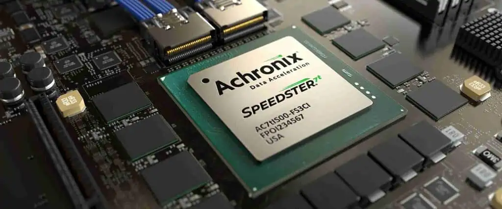
The Xilinx Spartan-7 family delivers an optimal balance of low cost, power efficiency and features in a small form factor FPGA. Built on an advanced 28nm manufacturing process, Spartan-7 provides high density logic, abundant IOs, integrated memory and DSP slices to address diverse embedded applications.

This article provides a comprehensive overview of the Spartan-7 architecture, available devices, key resources, datasheet specifications and reference design details. Comparison to previous Spartan generations is also included to illustrate the enhancements Spartan-7 delivers.

Spartan-7 Family Overview

The Spartan-7 family spans from 10K logic cells to over 200K logic cells across twelve device sizes to meet various application requirements:

This range of densities combined with low cost BGA packaging made Spartan-7 suitable for applications like display/camera interfacing, motor control, IoT edge nodes, industrial automation, and functional safety systems.

Now let’s explore the key resources and capabilities in more detail.

Spartan-7 Architecture Innovations

Building upon the popular Spartan-6 family, the Spartan-7 architecture incorporated new enhancements to deliver more application value at lower power.

28nm Process for Higher Density and Performance

The 28nm high-performance, low-power (HPL) manufacturing process allowed a 2X increase in logic density versus Spartan-6 built on a 45nm node. This expanded capacity within existing small form factors.

Higher transistor densities and lower supply voltages also enabled up to 25% power savings together with improved speed. Spartan-7 could operate across a wide 0.8V to 1.0V Vcc range.

Advanced Productivity Features

To boost design productivity, Spartan-7 added advanced capabilities like:

  • 150MHz+ speed grade devices
  • Integrated memory controllers with ECC support
  • Mixed-mode clock management blocks
  • Enhanced DSP blocks with 25 x 18 multipliers
  • Automotive and industrial temperature support
  • Feature-rich IO logic with DDR3 memory interfacing

These features facilitated integration of both control and data processing within a single Spartan-7 device.

Integrated Memory Controllers

To efficiently interface to external RAM and flash, Spartan-7 incorporated dedicated memory interface blocks. Key benefits included:

  • 1Gbps performance with 32-bit DDR3 support
  • Error correction code (ECC) logic for reliability
  • Simple interfacing without consuming programmable fabric resources
  • Reference designs to quickly leverage memory controllers

Low Cost Packaging and IP

Spartan-7 leveraged low-cost chip-scale ball grid array (CSBGA) packages making them ideal for price-sensitive, high volume applications.

Xilinx also provided a large catalog of free IP to accelerate designs including AXI peripherals, verification cores, DSP and video analytics functions.

Together these enhancements expanded Spartan-7’s capabilities compared to prior generations for embedded systems requiring integrated control, data processing and connectivity.

Spartan-7 FPGA Feature Details

Now let’s take a closer look at the details and specs behind the major resource types in Spartan-7 FPGAs.

Programmable Logic Blocks

The Spartan-7 logic fabric is organized as Configurable Logic Blocks (CLBs) interconnected through a hierarchy of routing resources.

Key attributes of the CLB architecture:

  • Each CLB contains 8 LUTs and 16 flip-flops
  • LUTs can also be configured as distributed memory or shift registers
  • 16-bit shift registers enhance high-speed datapath capability
  • 2 x 2 flip-flop pairs support high-fanout clocking
  • Fast carry logic for arithmetic operations

In total Spartan-7 delivers 19K to 147K LUTs to implement glue logic, state machines, buffers and other control-oriented functions.

Block RAM Memory

Spartan-7 contains 216Kb to 2.7Mb of embedded block RAM memory for data storage and buffering needs.

Block RAM provides:

  • Dual-port 18Kb blocks with optional ECC support
  • Configurable as 36Kb simple dual-port RAM
  • Built-in FIFO capability
  • Dedicated memory interface with DDR3 support and up to 10Gbps throughput

Abundant block RAM enables Spartan-7 to accommodate local data storage and buffering requirements.

Digital Signal Processing

For signal processing, math and vector operations, Spartan-7 integrates up to 444 DSP slices.

DSP slice features include:

  • 25 x 18 multipliers yielding 450 GMACS throughput
  • 48-bit accumulators for high precision compute
  • Cascadable to form wide math functions
  • Optional pipelining for high throughput
  • Power saving clock gating

The DSP slices readily support functions like filters, FFTs, matrix operations, video overlays and sensor fusion.

High Speed Serial I/O

To enable high bandwidth interfacing, Spartan-7 incorporates up to 12.5Gbps serial transceivers supporting protocols including PCIe, Ethernet, DisplayPort and SATA.

Key attributes of the serial transceivers:

  • Integrated high-speed analog for reduced BOM
  • Low power modes for 10G+ operation under 2W
  • Multi-rate capability from 500Mbps to 12.5Gbps
  • Sophisticated equalization for backplane signal integrity
  • Support for 150m copper cable lengths

Mixed-Mode Clock Management

Flexible clocking capabilities are provided through up to 12 mixed-mode clock management (MMCM) blocks and 48 clock management tiles (CMT).

Key clocking features include:

  • Zero delay buffers to reduce skew
  • Frequency synthesis, division and spreading
  • Phase shifting for timing adjustment
  • Low jitter PLLs for clock clean-up
  • Glitchless clock multiplexing and gating

Integrated Memory Controllers

As mentioned earlier, dedicated memory interface blocks enable interfacing to external DDR3 components.

Spartan-7 memory controllers provide:

  • 32-bit interface up to 1Gbps throughput
  • Simple SPI control for configuration
  • ECC support for reliability
  • Reference designs available
  • 1-2 controllers per FPGA device

Spartan-7 FPGA Datasheet Details

Xilinx provides comprehensive datasheets detailing the complete specifications and characteristics of Spartan-7 FPGAs. Let’s go through some of the key parameters covered:

Features Summary: Overview of device size, package offerings, process node, voltage, operating temperatures, etc.

Pinouts: Diagrams showing pin functions for each package footprint. Details I/O bank assignments.

Memory Ports: Specifications for block RAM capacity and configuration for each device size.

I/O Characteristics: AC/DC parameters for memory interface pins and general purpose I/Os. Highlights sideband signals like dedicated clock inputs.

Maximum Ratings: Absolute maximum voltages, junction temps, power consumption and other parameters. Ensures reliable operation when conditions are within ratings.

Thermal Resistance: Resistance parameters to estimate die temperature based on package thermal characteristics and power dissipation.

Switching Characteristics: Timing specs for global clocks, block RAM, transceivers and I/O interfaces across speed grades, voltage and temperature.

Power Consumption: Typical static and dynamic power consumption figures to estimate device power across use cases. Power varies by utilization.

Physical Attributes: Dimensions and weight for each package footprint. Helps with board layout and mechanical considerations.

System Signals: Descriptions of key clocks, configuration pins and other global signals used to operate the FPGA.

The comprehensive datasheet gives designers detailed electrical and physical data to properly model, analyze and deploy Spartan-7 devices in their systems.

Spartan-7 Reference Design Overview

To accelerate adoption, Xilinx provides a suite of Spartan-7 reference designs showing optimal utilization of resources:

Spartan-7 Evaluation Kit: Highlights main Spartan-7 feature sets like block RAM and DSP designs.

Memory Interface Solutions: Demo projects for integrating Spartan-7 memory controllers.

PCI Express Solutions: Endpoint demos using integrated PCIe blocks.

Connectivity Solutions: Networking and interfacing demos leveraging Spartan-7 transceivers.

Signal Processing Solutions: DSP pipeline designs for common algorithms like FIR filtering and FFT.

Video and Image Processing: Demos for video buffering, overlays, encoding using Spartan-7’s dedicated resources.

Industrial Networking and Motor Control: Real-world industrial app examples for functional safety and motor actuation.

These optimized reference projects enable faster design starts leveraging Spartan-7 capabilities. The source code can be readily modified and enhanced to meet application requirements.

Spartan-7 vs. Spartan-6 Comparison

To appreciate the enhancements in Spartan-7, it is useful to compare against its predecessor Spartan-6 built on 45nm technology:

Spartan-6

  • 45nm process node
  • Up to 150K logic cells
  • 3.2Gbps integrated serial transceivers
  • 200MHz speed grade
  • No integrated memory controller

Spartan-7

  • 28nm process enabling 2X density
  • Up to 275K logic cells
  • 12.5Gbps integrated serial transceivers
  • 150+ MHz speed grades
  • Integrated DDR3 memory controller

The combination of advanced process technology and architectural enhancements solidiified Spartan-7’s position as the leading low-cost/high-value FPGA offering at 28nm.

Conclusion

The Xilinx Spartan-7 family delivers new levels of design value through density, bandwidth and power improvements over prior generations. The 28nm manufacturing combined with 2X capacity, abundant memory, 12.5G serial connectivity and integrated DDR3 memory controllers cement Spartan-7’s standing as the premier low-cost FPGA.

For embedded applications like industrial networking, motor control, functional safety and IoT edge processing, Spartan-7 provides an optimal balance of features and small form factor. The comprehensive datasheet contains complete electrical specifications to aid design and analysis. Example reference designs allow accelerating time-to-market.

Overall, Spartan-7 carries forth Xilinx’s legacy of providing low-cost, high-value FPGAs for space-constrained embedded applications not requiring maximum capacity or performance. The family sets a new benchmark for low-cost programmable logic capability.

Spartan-7 FPGA FAQ

Here are some common questions regarding the Spartan-7 FPGA family:

Q: What process node is Spartan-7 manufactured on?

A: Spartan-7 uses a high-performance, low-power 28nm node to enable higher density and lower power versus the preceding 45nm Spartan-6 generation.

Q: Does Spartan-7 support 3.3V I/O signaling?

A: Yes, in addition to 1.8V interfaces Spartan-7 supports 3.3V I/O for legacy system interoperability along with mixed-voltage I/O banks.

Q: How many clock management tiles does the Spartan-7 architecture contain?

A: Spartan-7 contains up to 12 MMCM blocks and 48 CMTs for advanced clocking capability relative to device size.

Q: What embedded memory controllers are integrated in Spartan-7?

A: Integrated DDR3 memory controllers with 32-bit interface up to DDR3-1066 speed are included to interface to external RAM and SDRAM.

Q: Does Spartan-7 support PCI Express integration?

A: Yes, selected devices include integrated PCIe blocks for implementing PCIe endpoint connectivity without consuming FPGA fabric resources.

Working with electronics can be a terrifying prospect for someone who has little to no experience. One needs to be competent in several different areas just to get started. Fortunately, some tools can help simplify the process, and with these tools, any beginner can get off the ground running.

Xilinx Spartan-7 FPGA boards‘ design is precisely for this purpose with features. For instance, being free from onboard power supplies and simple USB connections. It makes the task of getting started easier than ever before.

The boards are essential in creating many things, from simple LED projects to clocks to full-featured computers, and much more. Spartan-7s is facing criticism from those who believe there is little to offer those with the most limited needs despite their versatility. This notion stems from the fact that many people see them as a steppingstone towards something better. It seems like a common opinion amongst those who do not know why they would choose Spartan-7 over other FPGA boards.

The Arty family of Digilent boards aims to change this notion. These boards are perfect for a wide variety of FPGA projects and do not require heavily trained engineers to use or operate. These designs combine power and ease of use with the flexibility needed to create something great. They also integrate high-end FPGA features. For instance, Xilinx‘s 1.2TFLOPS Tri-core processors, the industry-standard BM3358 dual-core processor, and more into small form factor boards that people can use. At the same time, they learn FPGAs without feeling overwhelmed by the technology.

Product description

The first thing that people will notice is that the Arty boards are small, just 4.75 inches by 2.8 inches. This makes them perfect for projects within tight spaces where it would be impossible to fit something larger. Since these boards lack onboard power supplies, they are straightforward to use since we can power them through any micro-USB cable or adapter. This makes them great for projects that might need relocation frequently. We do not need a particular power source to power the board once everything is working correctly.

In addition to being small, the boards are relatively light, making them easy to carry around or carry in a case. With a weight of just Under 1.5 pounds, most people who use them will not even know that they are carrying around an FPGA board.

The boards have all the standard functionality you expect from a modern FPGA board. They include Xilinx’s DSP blocks, such as the CINCH mode, and PCR blocks, such as the DSPax2 and DSPz2 cores. This helps to ensure that those who use these boards will be able to create something truly amazing without compromising the internal functionality of the board.

Each of these boards has several different design areas in mind. For example, the Arty 1 and Arty 2 boards place a significant emphasis on power and ease of use out of the box. With both boards, all needed to get started is a micro cable and any composite cable. Ones that you might need for your project already soldered to the board itself.

Xilinx Spartan-7 FPGA Boards Features

xilinx spartan 7 fpga

The Arty boards are the first FPGA boards that have Digilent’s new Artix-7 FPGAs. Both boards use the same basic schematic. However, they differ in handling power and forgo onboard power supplies to ensure that the boards are small enough to be portable.

Configuration

Configuring the Xilinx Spartan-7 FPGA boards is relatively easy. However, it can be confusing for those who have little to no experience with programming FPGAs. In all reality, this process is not difficult, and it simply takes time to learn how everything works.

You first need to use Xilinx’s WebPACK tools to configure the Artix-7 FPGA on either of these boards. The JTAG debugger that you need to do this comes with the board when you buy it. These boards also come with two micro-USB cables so that you can plug them into your computer.

Each of these boards has a Pmod connector so that you can use Digilent’s Pmod peripherals with the board. The connectors are compatible with the older Pmods, so any Pmod peripheral will work without issue. SPI Flash drives or JTAG debugger cards are beneficial with these boards. This is because they allow you to store files on them for easy transfer to other devices instead of transferring files to an SD card.

Support The Digilent Pmod peripherals work great with both boards, but the documentation can be confusing. The “Getting Started” section in the user manual says nothing about using them. The Pmod peripheral pages often list features that do not exist (for example, there is no six-channel A/D). QSPI flash drives with the Arty boards work, but they do not support multi-bit reads and writing like the SuperCap and Spark boards do.

Memory

Because these boards only come with 8MB of onboard memory, you will need to add at least one additional memory chip if you wish to store data and programs on the board itself.

The memory on these boards can last for a while, and it is unlikely that you will run out of space while working on something. The documentation lists the memory as being dynamic, but this is inaccurate. More accurate information is that you can write the memory, but it will not disappear.

Processors

These boards have two different processors onboard. The first is a single-core processor known as the TriCore processor, which functions at 633MHz. It has 4kb of embedded DDR2 RAM and 8kB of embedded SRAM.

The second processor is the BM3358 dual-core processor, which functions at 400MHz with two MB of embedded DDR2 RAM and 16kb of embedded SRAM. It also has 4kb of EEPROM to store configuration data.

The two processors are different in terms of how they operate, but they both function well. You can use these processors independently or together to do different things at the same time.

We should use the TriCore processor for low-power applications. This is because it requires very little energy to run, and it will not consume much power. The BM3358 is better suited for high-power applications since it can consume more energy than its companion chip.

Control & I/O

The Arty 1 and Arty 2 boards have a single user I/O port, allowing an external to wire the switch to the board. This allows the board to work as a simple switch, and it is beneficial for projects that need more than one piece of equipment to work simultaneously.

The boards also have a single DIP switch, allowing five different serial ports to connect to the board. This will enable you to use the boards with a variety of software tools and peripherals.

Both boards have a standard JTAG port that can debug code or use the board as a programmer. The Artix-7 FPGA also has an embedded serial port, but neither of these two boards has this feature. User pushbuttons are available for them, but they are somewhat limited in what you can do with them.

Both boards have 16 digital I/O pins that we can use to send or receive data. They also have four analogs PWM channels that can process their inputs or output data. This makes both boards extremely useful for HMI applications. It is because you can use PWM channels to display any image, text, or anything else that you might need on the screen. DIP switches are available to control the digital I/O pins and run a simulation to determine what they do.

The Arty 1 and Arty 2 boards can work as a general-purpose development board that we can use for various projects. The TriCore processor on these boards will not carry heavy loads very well, but it will manage those loads without issue if you need it to run programs.

Expansion Connectors

The Digilent Artix-7 Spartan-7 FPGA boards come with a variety of expansion connectors. It allows users to connect the boards to their other hardware.

The first expansion connector these two boards have is a Pmod connector. It allows the connection of other Digilent peripherals to the board. We can use them with both boards, but they will not work with the XC7A200T FPGAs on the Spark Board or SuperCap. VITA 57.1 FMC LPC connector This FMC connector allows users to connect a VITA 57.1 programming board to the board. There is no documentation on the Internet for this device. So, it may be easy to use wrong or damage something during the process.

The Digilent Artix-7 Spartan-7 FPGA boards have an LPC connector. So, users can program their peripherals instead of using the Xilinx software tool. Pmod Headers This connector allows users to connect an external display with a separate power supply to the board.

This adapter will allow users to connect an external USB flash drive to the board. You must connect it in this format, or it will not work correctly. This connector tells the board what memory banks are available on the expansion header. The only free bank on this board is A0, so if you do not have one of these connectors, you will not connect your expansion device to the board.

Communication & Networking

FULL PCB MANUFACTURING Quote

These boards can connect to any other piece of equipment you might have, but they can also communicate with each other.

The Artix-7 FPGA on the Arty 1 and Arty 2 boards comes with several built-in Ethernet channels that connect Ethernet-capable peripherals.

Arc Risc is an architecture created by Digilent that allows users to connect different boards over Ethernet. The UART to USB Bridge allows any USB device to connect to the board using a universal serial bus. This will allow you to use a variety of peripherals with these boards, but it will not allow the boards to communicate with each other.

The XADC-4096 can also connect to the two boards via Ethernet, but it is essential in sensing data from a piece of equipment that is not an Arty board. The RJ-45 Tri-Speed Ethernet Connectors can connect other boards because they have an RJ-45 connector to plug the cable into. This is not a common feature for FPGAs, but it can be helpful in a variety of applications.

These two boards have two different ways of allowing the user to connect their board to other equipment. The first way is with a USB cable because it enables you to move data between your board and any other piece of equipment that has a USB port.

Display

The Arty boards have a DSI LCD connector that allows the user to connect a TFT LCD or a digital micro-mirror display. This connector drives the display directly and ensures nothing is wrong with the data it is receiving. The TriCore processor on these two boards will also be able to drive the same displays. However, it will not do so since it cannot change the contrast or other settings on these displays. The HDMI Video Output on these boards will allow you to connect your board to an HDMI-capable display.

The Artix-7 FPGA on the Arty boards also has two DSI connectors that will allow you to connect a digital micro-mirror display or TFT LCD. The only difference is that the user must provide their power to the device instead of a USB cable. Additionally, the MIPI-CSI Camera Interface connector available on the Arty 1 and Arty 2 will let you connect a camera to these boards. Also, we can use the MIPI-DSI Display Interface to connect any TFT LCD. The DSI connector on the Arty boards also has an HDMI connector so that you can connect your board to an HDMI-capable display.

The Ralink RT5350F Wifi USB adapter for these boards can connect your board to any other device with a wireless network connection. The only problem with this adapter is that it does not have an antenna. So, if you are using it for anything more than basic programming, you will need to figure out how to increase the range of your wireless network.

Clocking

These boards come with several different clock speeds available for users to use. These clocks allow you to adjust the speed at which the FPGA is working, but they must have an appropriate voltage to run from.

The Arty boards have a VHDL source used for all their I/O signals. It is also the same as the clock used during normal operation, so there is no need for a clock input on these boards. The board will automatically adjust to a stable clock speed depending on the voltage that it gets. You can adjust the clock speed that it runs at using either of these two controls. The Artix-7 FPGA on these boards creates an internal gyroscope that will adjust the clock speed depending on moving.

The Artix-7 FPGA on these boards has two different clock outputs that you can use with external oscillators to drive it at different speeds. The first is the WANCOOP1 output which we use with external oscillators. It has an I2C Programmable Clock input, creating any clock speed that the user would like. The second clock output is CWAN1, and we can also use it with external oscillators, but it cannot create any clock speeds.

Power

There are two different power inputs available for this board. The first is the USB connector that allows the user to supply it with either 3.3V or 5V of power. We can use it to charge a battery directly, but we cannot use it if an AC adapter has a bad connection to the board. We refer to the other power input on these boards as BATEN1, and it has a 6-pin connector that allows users to supply the board with 5V of AC power directly.

The Arty boards also use the same two types of power inputs, but they come with more combinations of power supplies that we can use. These boards come with a C10-C16 DC power input that will allow users to supply the board with any voltage between 10 and 16 VDC. There is also an AUXIN1 input that can supply the board with up to 3A of current.

Advantages of the Xilinx Spartan-7 FPGA Boards

The Spartan-7 FPGA on the Arty boards will bring a lot of advantages to any project you are working on. The integrated flash memory and USB connectors will allow you to load and transfer data between you and your computer at high-speed rates. The built-in power supply and clock generators will also help by eliminating the need for two additional parts. Still, there is no need to use built-in oscillators. This is because they cannot output as high of speeds as one can achieve using external oscillators. The wide array of Analog, Digital, I/O, and Interfaces make this board an ideal choice for almost any type of application.

The Xilinx Spartan-7 FPGA on these boards is the same as the one found on the Wonder Boards. It has many of the same features, but some additional features are not available on the Wonder Boards. The TriCore processor will drive more digital displays than a single TriCore processor can drive on a Wonder Board. The DSI connectors will be able to drive more displays, but the Artix-7 FPGA on these boards will not drive the same amount as a Wonder Board.

The Xilinx Spartan-7 FPGA on these boards also has two built-in oscillators that come at different speeds. So, their outputs will need amplification if you are planning to use them with an external oscillator. Working with top PCB companies such as RayMing PCB and Assembly will help you enjoy all the advantages stated above.

Limitations of the Xilinx Spartan-7 FPGA Boards

One of the most significant limitations these boards face is requiring an external oscillator to use with projects. The internal oscillators will not work since they are only allowed to output at slower speeds. This limits what types of projects we can do with these boards. If you plan to use them for applications where you need the fastest possible clock speeds, you should choose a board from one of the other series of boards from Xilinx. However, they all have more limited features than the Spartan-7 FPGA on these boards.

Another limitation that these boards have is that there are only two I/O connectors available. The Arty boards have a USB connector available, but they can only charge a battery connected directly to the board. We can use the Artix-7 FPGA on the Arty boards to charge a battery connected directly, but there is no option for an external power source. The only I/O connector available for the Arty boards is an Analog Input connector. However, you cannot use them to connect any digital signals made on the Artix-7 FPGA. This does not limit what types of projects we can do, but it will make using them for some applications more difficult.

The Spartan-7 FPGA on these boards does not come with built-in oscillators.

Examples of Xilinx Spartan-7 FPGA Boards

spartan 7 vivado

[XCM-026Y] Xilinx Spartan-7 FGGA484 FPGA board (5 V Tolerant)

  • XC7S100: 160 DSP Slices, 4,320 Total Block RAM (Kb), 100 Maximum user I/O pins (Board), 338 Maximum user I/O pins (Device), 1,100 Maximum Distributed RAM (Kbits), 102,400 Logic Cells, and 16,000 Slice
  • XC7S75: 140 DSP Slices, 3,240 Total Block RAM (Kb), 100 Maximum user I/O pins (Board), 338 Maximum user I/O pins (Device), 832 Maximum Distributed RAM (Kbits), 76,800 Logic Cells, and 12,000 Slices
  • XC7S50: 120 DSP Slices, 2,700 Total Block RAM (Kb), 100 Maximum user I/O pins (Board), 250 Maximum user I/O pins (Device), 600 Maximum Distributed RAM (Kbits), 52,160 Logic Cells, and 8,150 Slices

[XCM-026] Xilinx Spartan-7 FGGA484 FPGA board (5 V I/O)

  • XC7S100: 160 DSP Slices, 4,320 Total Block RAM (Kb), 100 Maximum user I/O pins (Board), 338 Maximum user I/O pins (Device), 1,100 Maximum Distributed RAM (Kbits), 102,400 Logic Cells, and 16,000 Slice
  • XC7S75: 140 DSP Slices, 3,240 Total Block RAM (Kb), 100 Maximum user I/O pins (Board), 338 Maximum user I/O pins (Device), 832 Maximum Distributed RAM (Kbits), 76,800 Logic Cells, and 12,000 Slices
  • XC7S50: 120 DSP Slices, 2,700 Total Block RAM (Kb), 100 Maximum user I/O pins (Board), 250 Maximum user I/O pins (Device), 600 Maximum Distributed RAM (Kbits), 52,160 Logic Cells, and 8,150 Slices

[XP68-06] Xilinx PLCC68 Spartan-7 FPGA Module

  • XC7S50: 5 CMT (MMCMx1+PLLx1), 50 Maximum user I/O pins (Board), 210 Maximum user I/O pins (Device), 120 DSP Slices, 2,700 Total Block RAM Bits (Kbits), 600 Maximum Distributed RAM (Kbits), 52,160 Logic Cells, and 8,150 Slices
  • XC7S25: 3 CMT (MMCMx1+PLLx1), 50 Maximum user I/O pins (Board), 150 Maximum user I/O pins (Device), 80 DSP Slices, 1,620 Total Block RAM Bits (Kbits), 313 Maximum Distributed RAM (Kbits), 23,360 Logic Cells, and 3,650 Slices

[XCM-210] Xilinx Spartan-7 FGGA676 FPGA board

  • XC7S100: 296 Maximum user I/O pins (Board), 400 Maximum user I/O pins (Device), 8 CMT (MMCM x1 + PLL x1), 160 DSP Slices, 4,320 Maximum Block RAM (kb), 1,100 Maximum Distributed RAM (kb), 16,000 Slices, and 102,400 Logic Cells
  • XC7S75: 296 Maximum user I/O pins (Board), 400 Maximum user I/O pins (Device), 8 CMT (MMCM x1 + PLL x1), 140 DSP Slices, 3,240 Maximum Block RAM (kb), 832 Maximum Distributed RAM (kb), 12,000 Slices, and 76,800 Logic Cells

[XCM-308] Xilinx Spartan-7 FTGB196 FPGA board

  • XC7S50: 8150 Slices, 52160 Logic Cells, 600 Maximum Distributed RAM (kb), 2700 Maximum Block RAM (kb), 120 DSP Slice, 5 CMT (MMCMx1+PLLx1), 100 Maximum user I/O pins (Device), and 56 Maximum user I/O pins (Board)
  • XC7S25: 56 Maximum user I/O pins (Board), 100 Maximum user I/O pins (Device), 3 CMT (MMCMx1+PLLx1), 80 DSP Slice, 1620 Maximum Block RAM (kb), 313 Maximum Distributed RAM (kb), 23360 Logic Cells, and 3650 Slices
  • XC7S15: 56 Maximum user I/O pins (Board), 100 Maximum user I/O pins (Device), 2 CMT (MMCMx1+PLLx1), 20 DSP Slice, 360 Maximum Block RAM (kb), 150 Maximum Distributed RAM (kb), 12800 Logic Cells, and 2000 Slices
  • XC7S6: 56 Maximum user I/O pins (Board), 100 Maximum user I/O pins (Device), 2 CMT (MMCMx1+PLLx1), 10 DSP Slice, 180 Maximum Block RAM (kb), 70 Maximum Distributed RAM (kb), 6000 Logic Cells, and 938 Slices

[XCM-115Z] Xilinx Spartan-7 FGGA484 FPGA board

  • XC7A100T: 8 CMT (MMCM x1 + PLL x1), 160 DSP Slices, 128 Maximum user I/O pins (Board), 338 Maximum user I/O pins (Device), 4,320 Maximum Block RAM (Kbits), 1,100 Maximum Distributed RAM (Kbits), 102,400 Logic Cells, and 16,000 Slices
  • XC7S75: 12,000 Slices, 76,800 Logic Cells, 832 Maximum Distributed RAM (Kbits), 3,240 Maximum Block RAM (Kbits), 338 Maximum user I/O pins (Device), 128 Maximum user I/O pins (Board), 140 DSP Slices, and 8 CMT (MMCM x1 + PLL x1)
  • XC7S50: 5 CMT (MMCM x1 + PLL x1), 120 DSP Slices, 128 Maximum user I/O pins (Board), 250 Maximum user I/O pins (Device), 2,700 Maximum Block RAM (Kbits), 600 Maximum Distributed RAM (Kbits), 52,160 Logic Cells, and 8,150 Slices

[XCM-115] Xilinx Spartan-7 FGGA484 FPGA board

  • XC7A100T: 8 CMT (MMCM x1 + PLL x1), 160 DSP Slices, 128 Maximum user I/O pins (Board), 338 Maximum user I/O pins (Device), 4,320 Maximum Block RAM (Kbits), 1,100 Maximum Distributed RAM (Kbits), 102,400 Logic Cells, and 16,000 Slices
  • XC7S75: 8 CMT (MMCM x1 + PLL x1), 140 DSP Slices, 128 Maximum user I/O pins (Board), 338 Maximum user I/O pins (Device), 3,240 Maximum Block RAM (Kbits), 832 Maximum Distributed RAM (Kbits), 76,800 Logic Cells, and 12,000 Slices

[XCM-025Z] Xilinx Spartan-7 FGGA484 FPGA board

  • XC7S100: 8 CMT (MMCM x1 + PLL x1), 160 DSP Slices, 100 Maximum user I/O pins (Board), 338 Maximum user I/O pins (Device), 4,320 Maximum Block RAM (Kbits), 1,100 Maximum Distributed RAM (Kbits), 102,400 Logic Cells, and 16,000 Slices
  • XC7S75: 8 CMT (MMCM x1 + PLL x1), 140 DSP Slices, 100 Maximum user I/O pins (Board), 338 Maximum user I/O pins (Device), 3,240 Maximum Block RAM (Kbits), 832 Maximum Distributed RAM (Kbits), 76,800 Logic Cells, and 12,000 Slices
  • XC7S50: 5 CMT (MMCM x1 + PLL x1), 120 DSP Slices, 100 Maximum user I/O pins (Board), 250 Maximum user I/O pins (Device), 2,700 Maximum Block RAM (Kbits), 600 Maximum Distributed RAM (Kbits), 52,160 Logic Cells, and 8,150 Slices

[XCM-025] Xilinx Spartan-7 FGGA484 FPGA board

  • XC7S100: 8 CMT (MMCM x1 + PLL x1), 160 DSP Slices, 100 Maximum user I/O pins (Board), 338 Maximum user I/O pins (Device), 4,320 Maximum Block RAM (Kbits), 1,100 Maximum Distributed RAM (Kbits), 102,400 Logic Cells, and 16,000 Slices
  • XC7S75: 8 CMT (MMCM x1 + PLL x1), 140 DSP Slices, 100 Maximum user I/O pins (Board), 338 Maximum user I/O pins (Device), 3,240 Maximum Block RAM (Kbits), 832 Maximum Distributed RAM (Kbits), 76,800 Logic Cells, and12,000 Slices

[EDX-303] Xilinx Spartan-7 USB-FPGA board

  • XC7S100T: 4,320 Total Block RAM (kb), 56 Maximum user I/O pins (Board), 338 Maximum user I/O pins (Device), 1,100 Maximum Distributed RAM (kb), 102,400 Logic Cells, and 16,000 Slices
  • XC7S75T: 3,240 Total Block RAM (kb), 56 Maximum user I/O pins (Board), 338 Maximum user I/O pins (Device), 832 Maximum Distributed RAM (kb), 76,800 Logic Cells, and 12,000 Slices
  • XC7S50T: 2,700 Total Block RAM (kb), 56 Maximum user I/O pins (Board), 250 Maximum user I/O pins (Device), 600 Maximum Distributed RAM (kb), 52,160 Logic Cells, and 8,150 Slices

Conclusion

These boards are great supplements to any other board that you have for your project. You can use them to perform tasks that were once impossible because of the limitations of other FPGA boards. They do not offer as many features as the Arty family, but they still provide plenty of features to make them useful for almost any type of application. They are not as good as the Wonder Boards, but they are still high-quality FPGA boards.

How to use FTDI USB Fpga boards

FTDI USB boards

If you know where to go on the Internet, you can find a USB board already configured for FTDI connection. First, you need to check if your computer has a USB port, as you can use any USB-powered device to communicate with your FTDI device. Second, you need to connect the FTDI board to your computer with a USB cable. Third, within the driver, go onto the “Communication” tab and check that “USB Serial,” “USB Device Class,” and “USB Version” are all set to the right values.

After this, it is time to start working with your FTDI device! FTDI devices have many options, so many are not ready by default. Just google around to find out which settings you need for your specific hardware.

Among the settings that you may need to adjust in your FTDI device, you can find:

1. Set the baud rate.

Check the documentation of your device to say what value it needs.

2. Setting serial port parameters.

The FTDI board sets these automatically. However, if you have one of those USB devices which works with some other protocol (such as CAN Bus) or if you want to use hardware flow control, then set these parameters manually.

What is an FTDI chip?

ftdi usb

An FTDI chip is a small computer with one significant difference. Its pins connect to another electronic device instead of installing them into a circuit. Thus, we can use the FTDI chip to talk over an RS232 serial interface in any other electronic device.

There are many uses for an FTDI chip. For example, we can use it as a serial adapter to convert RS232 signals to USB so that you can use the host computer’s USB port with it. Or we can use it as a USB-to-RS232 converter to connect to a computer that does not have a built-in RS232 interface. Also, we can use it as a USB keyboard (hence its name).

Many of these applications were there before, with various results. But this time, I will describe how you could use your FTDI chip directly in your electronics project. I will assume that you are willing to do some soldering and have basic knowledge of electronics.

What are the advantages of using an FTDI chip?

Since the FTDI chip is a separate computer that we can buy for under $5, it is cheap to connect. In addition, because it uses its memory and processor while sharing a single interface with other devices, communication between the device and the FTDI chip is faster than communication between two computers using an RS232 cable.

Since there is no cable to connect, you can fit the device into much smaller spaces than if you had an RS-232 card. Generically, this means it will be easier for you to hide the chip from sight and deliberate observation by someone else.

The FTDI chip comes with drivers that should work without configuration on most Windows, Linux, and OSX machines. Hence, you can use it in a wide range of environments. There are even cases where you can plug an FTDI chip into your USB port, and it will work immediately. This is not always possible with RS232 cards that we need to configure for the operating system to recognize them.

It is very easy to connect almost any device to an FTDI chip. You need to read your hardware documentation, as there are usually no details about this specific feature.

Unlike an RS232 card that we may need to configure to work, the FTDI chip is always ready-to-use. There is no need for extra software or configuration. It will always work as soon as you plug it in.

One can send data, and you will never forget how to connect your device back and forth with an FTDI chip. You will never have to learn extra commands or settings for your hardware to work, but you can use any protocol you require.

Types

FULL PCB MANUFACTURING Quote

There are three main types of FTDI chips.

We also various manufacturers of these chips that include RayMing PCB and Assembly. But many use the same chipset and basic features.

FTDI Basic (V1.0)

The FTDI Basic (V1.0) is the oldest and the most basic of all the chips. It does not have any automatic reset, nor does it auto-disable for unused pins (“floating”). Also, it has a slight problem connecting to some USB ports at higher speeds.

We can find it in early FTDI cable products and most USB breakout boards.

FTDI Cable v2

There also exists an FTDI Cable v2. It has the same features as the FTDI Basic but uses two chips instead of one. It also has additional features such as automatic reset on power-up, auto-disable for unused pins, support of USB 2.0 speeds. There are some examples of this type in cables and USB breakout boards (for example, “FTDI Basic to USB Cable v2 โ€“ New”).

FTDI Basic v3

In 2009 there was a new type called the FTDI Basic v3.

The main difference is that it does not have the problem of connecting to a USB port that has a high-speed mode. Instead, it works only with a “fast” speed USB port, normally found on all modern computers. As a result, this is the only way to plug an FTDI Basic v3 cable into an “old” computer running Windows XP / Vista or Mac OS X and expect it to work.

The FTDI Basic v3 is available in most new cables and USB breakout boards.

FTDI cable v5

There is also an FTDI cable v5 which uses the same chipset as the FTDI Basic v3 but adds a new feature: auto-disable for unused pins.

It’s also now available in most new cables and USB breakout boards.

The difference between the FTDI Basic v3, the cable v5, and the original FTDI Basic is that they use entirely different chipsets (they do not share features).

FTDI Basic v3 and FTDI cable v5 share the same features, but the FTDI Basic v3 has 1.1V levels, while the FTDI cable v5 has 3.3V levels.

The original FTDI Basic is in level 0 (0V).

Note: If you want to buy one of these chips, please note that many fake versions are available on eBay and other sites. Please check with your seller for details of their guarantee and warranty.

The FTDI Cable v6

FTDI Cable v6 came in 2010 to replace the FTDI cable v5.

The main difference is that it has a higher voltage level (3.3V instead of 1.1V) and thus a greater distance for the current to flow without damage to the chip.

Also, it comes with improved software from cable v5. It has a new and easier method to configure your device using its application software and standard USB hub software.

The FTDI cable v6 is available in most new cables and USB breakout boards.

ft232r usb uart

Pin Configuration

The most common example is when you want to connect your Arduino board to the FTDI cable:

GND pin is the ground (commonly known as “-” or, on an Arduino board, some of the GND connections). The TXB pin is for sending data from the FTDI chip to your Arduino board. We need to connect this with the RXB pin on your Arduino.

The RXB pin is for receiving data from the Arduino board. So we need to connect this with the TXB pin on your Arduino.

Other devices may have different pinouts. However, they should be compatible as long as they fit into the same connections.

Newer FTDI chips are 5V tolerant, meaning they will not damage the Arduino board if abused by connecting it to a higher voltage. Still, other devices connected via an FTDI cable may suffer damage because they may not be 5V tolerant.

Downloading and installing the drivers

This can be very tedious since you need to download the correct driver for your operating system. You need to find the correct driver by following some steps:

  1. Download and install the free software “FTDI Driver Tool” from here
  2. Select “USB to Serial Adapter” from the devices menu in the FTDI driver tool.
  3. For Windows, click on the “Start” button and type “devmgmt.msc” into the search box on top of the window. Then press [Ctrl+E] and follow the steps to select “FTDI Device” from the device manager.
  4. For Linux, open a terminal window and type “lsusb” into the search box on top of the window to find the correct driver. Also, you can do a google search for “Linux USB serial adapter.”
  5. For Mac OSX, open a terminal window and type “ls -l /dev/cu.*” into the search box on top of the window to find the correct driver.

How to use FTDI USB to Serial Converter?

When you connect cable v5 to a computer, it will automatically reset and install its software on the computer.

You will then get an application called “FTDI Basic Control,” where you can configure your device.

One can also use the standard USB hub software supplied with most operating systems (for example, “WinUSB” in Windows 7). It helps to configure your device from another computer or control it from another application.

There is no need for any special tools to configure your device.

How to install the FTDI Basic Control software

To install this software, you will need to get the “Win32 Disk Imager” program from here and install it on your computer.

The program will then automatically install the FTDI Basic Control software.

Advanced configuration of the FTDI Basic Control software

The Advanced Configuration is only needed if you want to read or write directly to your computer’s serial COM port without using a virtual COM port. For example, to add advanced functionality to your project.

You will also need the “CMDebug” software from here.

It will show you detailed information about all the pins on both your FTDI USB-Serial Converter and your computer’s serial port.

The COM port and FIFO information are also displayed. It helps you use the standard “CMDebug” software to write to your computer’s serial port if you need to.

You may need to use this advanced configuration in rare circumstances. For example, if you want the complete I/O pins of the FTDI USB-Serial Converter to be available for your use.

FTDI Driver Installation

The FTDI driver installation will depend on your operating system.

In general, if you install the FTDI Basic Control software (the “FTDI USB-Serial Converter” control panel), then you should install the drivers automatically when you connect the cable v5 (OE/DO) to a computer.

Otherwise, you will need to install the drivers manually.

The FTDI Basic v3 is now obsolete. There are very few sellers of this chip in a new condition available on eBay and other sites. Check with your seller for details of their guarantee and warranty. FTDI has discontinued selling the FTDI Basic v2.

As of 2015 (and preceding years), there are very few sellers of this chip in a new condition available on eBay and other sites. Check with your seller for details of their guarantee and warranty.

The FTDI cable v5 chips are compatible with the FTDI Basic v2 and v3 cables.

However, the FTDI Basic v2 and v3 cables will not work properly with cable v5.

The general recommendation is to use the most up-to-date cable available for your system. You can use either the FTDI Cable V6 or a USB breakout board from Adafruit Industries.

It will provide better compatibility and more advanced features in most cases.

This chip has four wires. It is a popular chip, and many maker kits are available in new condition.

The FTDI Basic v4 is not compatible with cable v5 (OE/DO). It will only work with a cable v6 (OE/DI).

How to use FTDI chip in Linux

The FTDI USB-Serial Converter is a virtual com port device.

We can use it in Linux as a serial port device by accessing it through the /dev/ttyXX interface (where XX is “d,” “i,” “u,” or “g”).

One must set device permissions to mode 0666 before the Com port works (otherwise, the device will not be visible to the kernel).

Where d corresponds to 1.1V, I correspond to 3.3V, u corresponds to do 12V, and g corresponds to 5V (1.2V) (OE/DI mode only).

Check the output of lsusb for a line beginning with “bcdDevice” to determine the current mode.

The modes are set by inserting the OE/DI wire into a connection on the FTDI USB-Serial Converter and pressing the button on the converter.

For example:~$ echo 3 > /dev/ttyUSB0_0 sets it to Com port mode 3 (3.3V).

The user running udevadm can also change the USB.usermap files as a root user.

As of 2010, the “firmware” wheels available from FTDI only include drivers for Microsoft Windows (32/64-bit).

Compatible drivers for Linux exist in the kernel and are part of many distributions.

These drivers do not have the recent updates and are missing support for the latest chips.

Unfortunately, the current version does not support the newer chips.

FTDI series boards

Boards that belong to this category include:

[USB-101]FT2232H Evaluation Board

[USB-102]FT4232H Evaluation Board

[USB-103]FT2232H Evaluation Board Single type

Specifications (USB-101, 102, 103)

  • Made In Japan
  • Non-use of 6 Restricted substances of RoHS directive
  • Four-layer PCB with Immersion gold
  • EEPROM x1 (Mounted before shipment, Programmed)
  • Power LED
  • EEPROM Socket
  • Power-on reset IC
  • On-board 3.3V regulator
  • Selectable power source
  • 3-pin user interface (Channel B Tx and Rx)
  • 22-pin user interface (Channel A)
  • USB B-type connector

Specifications (FT2232H, FT4232H)

  • +3.3V single supply operating voltage range
  • Compact 64-LD Lead-Free LQFP or LQFN package
  • Extended -40ยฐC to 85ยฐC industrial operating temperature range
  • +1.8V and +3.3V I/O interfacing
  • USB Bulk data transfer mode
  • UHCI/OHCI/EHCI host controller compatible
  • Supports bus-powered, self-powered and high-power bus powered USB configurations
  • Low operating and USB suspend current
  • Configurable I/O drive strength (4, 8, 12, or 16mA) and slew rate
  • Auto-transmit enable control for RS485 serial applications using TXDEN pin
  • UART Interface has capability of supporting 1/2 stop bits, 7/8 bit data, and Even/Odd/Space/Mark/No Parity
  • Option for transmitting and receiving LED drive signals on each channel
  • Adjustable receive buffer timeout
  • Fast Opto-Isolated serial interface option
  • MCU host bus emulation/imitation mode configuration choice
  • CPU-style FIFO interface mode that streamlines design of CPU interface
  • Single-channel synchronous FIFO mode for transfers > 25 Mbytes/sec
  • USB to parallel FIFO transfer data rate of 10Mbyte/sec max
  • RS232/RS422/RS485 UART Transfer Data Rate to 12Mbaud max
  • Independent Baud rate generators
  • Whole USB protocol held on the chip. There is no specific requirements for USB firmware programming
  • Single-chip USB to dual parallel / serial ports with a diversity of configurations

[USB-106] FT600 Evaluation Board

[USB-107] FT601 Evaluation Board

Specifications (FT600, FT601)

  • Extended operating temperature range: -40 โ„ƒ to 85 โ„ƒ
  • Integrated power-on-reset circuit
  • Supports Remote Wake-up capability
  • Configurable GPIO support
  • Supports multi-voltage I/O: 1.8 V, 2.5 V, and 3.3 V
  • Up to 8 pipes or configurable endpoints
  • Supports multi-channel FIFO interface
  • Has Built-in 16kB capacity FIFO data buffer RAM
  • Supporting two parallel slave FIFO bus protocols, with data bursting rate to 400 Mbps max
  • Offers USB Battery Charger Recognition/Detection
  • Support for USB3.0 SuperSpeed, USB High Speed, and USB 2.0 Full Speed transfer

USB FPGA boards

USB FPGA board

[EDA-008]Altera Cyclone V USB-FPGA board

  • Altera 5CEBA4F23C8N: 100Maximum user I/O pins (Board), 224 Maximum user I/O pins (Device), 16 Global Clock Networks, 4 PLLs, 132 18 x 18 Multipliers, 3,383 Embedded memory (Kbits), and 49 K Logic Elements.

[EDA-011] Intel Cyclone 10 LP F484 USB-FPGA board

  • 10CL120YF484C8G: 100 Maximum user I/O pins (Board), 277 Maximum user I/O pins (Device), 4 PLL, 288 18×18 Multipliers, 3888 M9K Blocks (kb), and 119088 Logic Elements.
  • 10CL080YF484C8G: 100 Maximum user I/O pins (Board), 289 Maximum user I/O pins (Device), 4 PLL, 244 18×18 Multipliers, 2745 M9K Blocks (kb), and 81264 Logic Elements.
  • 10CL055YF484C8G: 100 Maximum user I/O pins (Board), 321 Maximum user I/O pins (Device), 4 PLL, 156 18×18 Multipliers, 2340 M9K Blocks (kb), and 55856 Logic Elements.
  • 10CL040YF484C8G: 100 Maximum user I/O pins (Board), 325 Maximum user I/O pins (Device), 4 PLL, 126 18×18 Multipliers, 1134 M9K Blocks (kb), and 39600 Logic Elements.
  • 10CL016YF484C8G: 100 Maximum user I/O pins (Board), 340 Maximum user I/O pins (Device), 4 PLL, 56 18×18 Multipliers, 504 M9K Blocks (kb), and 15408 Logic Elements.

[EDA-301]Altera Cyclone IV USB-FPGA board

  • The Altera EP4CE15F17C8N: 56 Maximum user I/O pins (Board), 165 Maximum user I/O pins (Device), 20 Global Clock Networks, 4 PLLs, 56 Embedded 18 x 18 multipliers, 504 Embedded memory (Kbits), and 15,408 Logic Elements.

[EDA-302]Altera Cyclone V USB-FPGA board

  • Altera 5CEBA4U15C8N: 56 Maximum user I/O pins (Board), 224 Maximum user I/O pins (Device), 16 Global Clock Networks, 4 PLLs, 132 18 x 18 Multipliers, 3,383 Total Memory (kb), 303 Memory: MLAB (kb), 3,080 Memory: M10K (kb), 18,480 ALM, and 49 K Logic Elements.

[EDX-008]Xilinx Kintex-7 USB-FPGA board

  • XC7K160T-1FBG484C:ย 8 CMT (MMCMx1+PLLx1), 600 DSP Slice, 11,700 Max Block RAM Bits, 100 Maximum user I/O pins (Board), 400 Maximum user I/O pins (Device), 2,188 Maximum Distributed RAM (Kb), 25,350 Slice, and 162,240 Logic Cells.
  • XC7K70T-1FBG484C:ย 6 CMT (MMCMx1+PLLx1), 240 DSP Slice, 4,860 Max Block RAM Bits, 100 Maximum user I/O pins (Board), 300 Maximum user I/O pins (Device), 838 Maximum Distributed RAM (Kb), 10,250 Slice, and 65,600 Logic Cells.

[EDX-301]Xilinx Spartan-6 USB-FPGA board

  • The XILINX XC6SLX16-2CSG225C: 576 K Total Block RAM bits, 56 Maximum user I/O pins (Board), 232 Maximum user I/O pins (Device), 136 K Maximum Distributed RAM bits, 14,579 Logic Cells, and 2,278 Slices.

[EDX-302] Xilinx Artix-7 USB-FPGA board

  • XC7A100T-1FTG256C: 4,860 Total Block RAM (kb), 56 Maximum user I/O pins (Board), 170 Maximum user I/O pins (Device), 1,188 Maximum Distributed RAM (kb), 101,440 Logic Cells, and 15,850Slices.
  • XC7A75T-1FTG256C: 3,780 Total Block RAM (kb), 56 Maximum user I/O pins (Board), 170 Maximum user I/O pins (Device), 892 Maximum Distributed RAM (kb), 75,520 Logic Cells, and 11,800 Slices.
  • XC7A50T-1FTG256C: 2,700 Total Block RAM (kb), 56 Maximum user I/O pins (Board), 170 Maximum user I/O pins (Device), 600 Maximum Distributed RAM (kb), 52,160 Logic Cells, and 8,150 Slices.
  • XC7A35T-1FTG256C: 1,800 Total Block RAM (kb), 56 Maximum user I/O pins (Board), 170 Maximum user I/O pins (Device), 400 Maximum Distributed RAM (kb), 33,280 Logic Cells, and 5,200 Slices.
  • XC7A15T-1FTG256C: 900 Total Block RAM (kb), 56 Maximum user I/O pins (Board), 170 Maximum user I/O pins (Device), 200 Maximum Distributed RAM (kb), 16,640 Logic Cells, and 2,600 Slices.

[EDX-303] Xilinx Spartan-7 USB-FPGA board

  • XC7S100T-1FGGA484C: 4,320 Total Block RAM (kb), 56 Maximum user I/O pins (Board), 338 Maximum user I/O pins (Device), 1,100 Maximum Distributed RAM (kb), 102,400 Logic Cells, and 16,000 Slices.
  • XC7S75T-1FGGA484C: 3,240 Total Block RAM (kb), 56 Maximum user I/O pins (Board), 338 Maximum user I/O pins (Device), 832 Maximum Distributed RAM (kb), 76,800 Logic Cells, and 12,000 Slices.
  • XC7S50T-1FGGA48C: 2,700 Total Block RAM (kb), 56 Maximum user I/O pins (Board), 250 Maximum user I/O pins (Device), 600 Maximum Distributed RAM (kb), 52,160 Logic Cells, and 8,150 Slices.

Conclusion

The FTDI Basic is the most varied of all the chips. However, we can modify it (for example, by adding a “floating” pin), and it works with practically any USB device.

Temperature and Humidity Sensor DHT11 vs DHT22 Which one is better

Temperature and Humidity Sensor DHT11 vs DHT22

Have you been searching for low-cost humidity and temperature sensors? Great timing! Here, we will discuss the DHT11 and DHT22. These are the two well-known humidity and temperature modules for Raspberry Pi and Arduino.

Though DHT11 and DHT22 are slower compared to some temperature sensors, both boast of benefits that include great long-term stability and low consumption of power. In addition, you can get relatively high accuracy in measurement at an affordable rate.

Both DHT sensors are great for any home project such as weather stations, inspection and testing of equipment, garden or farm monitoring systems, environmental control systems, and more.

DHT sensors are composed of two major parts. These include a thermistor having a basic chip and a humidity sensor. Both are responsible for converting from analog to digital.

What is DHT11?

DHT11 vs DHT22

DHT11 can be referred to as a basic, low-cost humidity and temperature sensor. It has the capability to detect relative humidity and temperature. The relative humidity here refers to the quantity of airโ€™s water vapor compared to the water vaporโ€™s saturation point in air.

Furthermore, DHT11 is widely regarded as the humidity and temperature module for Raspberry Pi and Arduino. Therefore, due to its many benefits, hardware enthusiasts favor the DHT11. Also the DHT11 humidity temperature sensor also works with respect to the new DHT11 module.

 Features

  • Consumes low power and has a great long-term stability
  • You can obtain a relatively high accuracy in measurements at a low and affordable cost
  • Range of humidity falls between 5 โ€“ 95% RH, and having a ยฑ5%. Also, the range of temperature falls within -20 – 60โ„ƒ and having a ยฑ2%.

Comparing the old and new DHT11, we can see some differences. The old DHT11 is called ADSONG, while the new is ASAIR.

  • The old DHT11 has a resistive sensor, while the new DHT11 has a capacitive sensor
  • Old DHT11 has a humidity range falling between 20 and 95%, while the new DHT11 has a humidity range that falls between 5 and 95%
  • The old DHT11 has a temperature range falling between 0 and 50โ„ƒ, while the new DHT11 has a temperature range that falls between 20 and 60โ„ƒ.
  • The old DHT11 has a temperature resolution of 1โ„ƒ, while the new DHT11 has a temperature resolution of 0.1โ„ƒ.

From this comparison, you can clearly see that the new DHT11 has a wider range for both humidity and temperature. Furthermore, its temperature resolution is also lower.

What is DHT22?

DHT22 is also referred to as RHT03 or AM2302. The DHT22 features a temperature sensor with high precision, as well as a humidity sensor. It makes use of a digital module acquisition technology, as well as humidity and temperature sensing technology. This is just to ensure that it is highly reliable and has great long-term stability.

Furthermore, DHT22 features a sensing element, as well as a measuring element of temperature of high precision, which is connected to an 8-bit microcontroller of high performance. Therefore, it has great quality benefits, very quick response, high-cost performance, and high anti-interference ability.

Features of the DHT22

  • Its size is ultra small
  • Power consumption is extremely low, coupled with a distance of signal transmission of over 20 meters. Therefore, it can withstand applications that are most demanding.
  • Range of the humidity sensor falls between 0 โ€“ 99.9% RH, and has an accuracy of ยฑ2%. Also, the range of temperature falls within -40 – 80โ„ƒ and has an accuracy of ยฑ0.5โ„ƒ.

Note that the sensor module can be sold individually. Also, connection with 3 leads is easy. If you wish to connect the sensor using a longer wire, all you need to do is include a pull-up resistor.

What are the Differences: DHT11 vs DHT22

FULL PCB MANUFACTURING Quote

Temperature range: With respect to the temperature range, for DHT11, it falls within -20 – 60โ„ƒ, while for DHT22, it falls within -40 – 80โ„ƒ.

Temperature accuracy: DHT11 has a temperature accuracy of ยฑ2%, while that of DHT22 is ยฑ0.5โ„ƒ

Humidity Range: the humidity range for DHT11 falls between 5 โ€“ 95% RH, while that of DHT22 falls within 0 โ€“ 100%RH.

Humidity Accuracy: DHT11 has a humidity accuracy of ยฑ5%, in contrast to DHT22, which is ยฑ2%.

Cost: The cost of DHT11 is $5.90 compared to that of DHT22, which is $9.90.

In conclusion, in all aspects, the DHT22 beats the DHT11. This includes humidity accuracy, humidity range temperature accuracy, and temperature range. DHT22 has just one downside, which is its higher price compared to that of DHT11. However, this is necessary, since you have to pay more to get the better deal.

Therefore, if you are searching for a sensor having a wider accuracy and range, then you should choose the DHT22. However, if you decide to choose the DHT11, no problem; it will also work well for your different projects.

Generally, both DHT sensors are regarded as slow and basic humidity and temperature sensors, which are great for hobbyists and beginners seeking to do some data logging. Both utilize one digital pin and function very slowly. You cannot query both sensors more than once for each second.

How do DHT11 and DHT22 sensors Interface and Work with Arduino?

Before we go into details on how DHT11 and DHT22 sensors interface and work with Arduino, letโ€™s first consider how the two sensors work.

Working Principle of the DHT11 and DHT22

Here, we will be considering how the DHT11 and DHT22 sensors work. They are made up of a thermistor or temperature sensor, a component for humidity sensing, and an integrated circuit on the sensorโ€™s back side.

For the measurement of humidity both sensors make use of a sensing component having two electrodes with a substrate for holding moisture between them. As changes in humidity happen, the substrateโ€™s conductivity changes, or changes happen in the resistance found in between the electrodes. The IC measures and processes the resistance change. By doing so, it prepares it for reading by the microcontroller.

Measuring the temperature, on the other hand, both sensors utilize a thermistor or a NTC temperature sensor. A thermistor can b e referred to as a resistor that changes the resistance value with temperature change. The manufacturing of these sensors came to be by sintering semi-conductive materials like polymers and ceramics, so as to offer larger resistance changes with just little temperature changes.

NTC refers to the โ€œNegative Temperature Coefficient.โ€ This means that there is a decrease in resistance with every temperature increase.

Circuit Schematics

Sensors DHT11 and DHT22 feature four pins โ€“ data pin, VCC, an unconnected pin, and GND, with all four having no usage. Thereโ€™s a need for a pull up resistor from 5-10 ohms to ensure the data line is kept high to ensure that there is a communication between the Arduino board and the sensor. Some of these sensorโ€™s versions feature breakout boards having an in-built pull-up resistor having only 3 pins.

Both sensors feature their personal single wire protocol. These are used in data transfer. This protocol also requires accurate timing. Also, you will find the diagrams required for getting this data from both sensors on their datasheets. However, thereโ€™s no need to be concerned about the timing diagrams. This is because the DHT library will be useful here as it handles everything.

Pinout of the DHT11 and the DHT22

It is fairly easy to connect both sensors โ€“ DHT11 and DHT22. As mentioned earlier, they feature four pins.

VCC pin: This pin provides the sensorโ€™s power. Although the voltage supply falls between 3.3V โ€“ 5.5V, it is recommended to work with the 5V supply.

As regards the power supply of 5V, the sensor can be kept for about 20 meters. In contrast, for the supply voltage of 3V, the length of the cable cannot be more than a meter. If this happens, the line voltage will drop, thereby causing measurement errors.

Data Pin: The data pin is the medium through which the microcontroller and the sensor communicates

NC: This means not connected

GND: This pin has to be connected to Arduinoโ€™s ground.

Connecting the DHT11 and DHT22 to the Arduino UNO

By now, you should have a good understanding of the way DHT sensors function. Now, we can start connecting it to the Arduino.

Fortunately, it is not important to connect both sensors – DHT11 and DHT22 โ€“ to Arduino. Their pitch pins of 0.1 inches are fairly long; therefore plugging them into breadboards will come in. Using the 5V, power up the sensor and then connect them ground to ground. Lastly, connect the digital pin #2 to the data pin.

Also, you need to place a resistor (pull-up) of 10Kฮฉ between the data line and the VCC to ensure it is kept HIGH. This makes proper communication between the MCU and the sensor. However, if you possess the sensorโ€™s breakout board, then thereโ€™s no need to include an external pull-up. Also, it features a pull-up in-built resistor.

After achieving this, you can now go ahead with uploading some code and get it to work.

Printing of Values on the Serial Monitor

Both sensors, DHT11 and DHT22 feature their personal single wire protocol, which are utilized for data transfer. Thereโ€™s a need for precise timing for this protocol. Fortunately, you donโ€™t have to be bothered about this. This is because everything will be taken care of by the DHT library.

First download the library here, and then install it. To do the installation, open your Arduino IDE โ€“ Sketch โ€“ Include Library โ€“ Add .ZIP Library, then lastly, select the file that you have just downloaded. However, if you need more information on how to install the library, you can use this tutorial.

After installing the library, copy the sketch into your Arduino IDE. This test sketch helps in printing the values of the relative humidity and temperature on your serial monitor. Letโ€™s explain this sketch in detail.

After uploading the sketch, you will see a window that reveals the output delivered by Arduino.

Explanation of the Code

The sketch begins by the inclusion of the DHT library. Then, we have to define the pin number of the Arduino to which the data pin of our sensor is connected; we then use it in creating a DHT object. By doing so, we will be able to access any special function that relates to the library. This is shown below:

  • #include <dht.h>
  • #define dataPin 8 // Defines pin number to which the sensor is connected
  • dht DHT; // Creats a DHT object

For the โ€˜setupโ€™ function, thereโ€™s a need to initiate serial communication, because this serial monitor will be useful in printing the results. This is shown below:

  • void setup() {
  •      Serial.begin(9600);

For the โ€˜loopโ€™, we will be utilizing the function read22(). This reads the DHT22 data. It takes the data pin number of the sensor as one parameter. You can make use of the read11() function if youโ€™re tinkering using DHT11. This can be achieved by uncommenting the second line like this:

  • //Uncomment whatever type you’re using!
  • int readData = DHT.read22(dataPin); // DHT22/AM2302
  • //int readData = DHT.read11(dataPin); // DHT11

As soon as you have the values for the temperature and humidity calculated, you can easily access them this way:

  • float t = DHT.temperature; // Gets the values of the temperature
  • float h = DHT.humidity; // Gets the values of the humidity

Now, the DHT object returns the value of the temperature in degrees Celsius. You can convert it to degrees Fahrenheit using this:

  • //print the temperature in Fahrenheit
  • Serial.print((t * 9.0) / 5.0 + 32.0);

Conclusion

Concerning precision, that of DHT11 is lesser than that of DHT22. It functions in a much smaller range of humidity and temperature. Asides from this, it is a bit slower, price point is lower, and its form factor is smaller too. If you desire some accuracy for your project, and you are okay with its higher price, then you should choose the DHT22. However, if this is not the case the DHT11 works fine. You can decide to work with any of the two.

What is Xilinx Virtex-5 FPGA ?

Xilinx Virtex-5 fpga

Introduction

The Xilinx Virtex-5 FPGA family was unveiled in 2006, providing new levels of capability through 65nm process technology along with novel architectural enhancements. Virtex-5 cemented Xilinx’s technology leadership for years following its introduction.

Virtex-5 implemented numerous innovative features including embedded processors, high-speed serial I/O, advanced clocking and power management techniques. These came together to enable a giant leap in bandwidth, efficiency and ease-of-use compared to prior Virtex generations.

This article will dive into the key innovations of Virtex-5 to understand what made it a milestone in FPGA history and a popular choice for high-performance applications. Comparison to predecessor and successor families is also provided for context.

Virtex-5 FPGA Family Overview

The Virtex-5 family consists of seven platforms tailored to different application needs:

  • LXT – High performance logic
  • SXT – Signal processing
  • TXT – High IO bandwidth
  • FXT – Low power
  • HXT – Automotive
  • QXT – Military qualified
  • CXT – Commercial space ready

With up to 8 billion transistors and gate counts up to 2 million, Virtex-5 was the most capable FPGA when introduced.

Some of the common features across Virtex-5 platforms include:

  • 65nm process technology
  • Embedded PowerPC processors
  • High speed serial transceivers up to 11.2Gbps
  • Advanced clock management techniques
  • Enhanced DSP48E slices
  • Multi-gigabit memory bandwidth

Let’s look at some of the major innovations driving Virtex-5’s leadership performance.

65nm Process Technology

Xilinx Virtex-5 fpga

The Virtex-5 family leveraged a high-performance triple-oxide 65nm manufacturing process with nine layers of copper interconnects. This enabled much higher logic density, performance and lower power consumption compared to previous 90nm nodes.

Some of the benefits of 65nm technology include:

  • 2X logic capacity over preceding Virtex-4 generation
  • Faster transistors enabling 30% higher speed or 25% lower power
  • 1.2V core voltage resulting in significant power savings
  • Tighter design rules producing smaller die sizes

The 65nm node gave Xilinx a multi-year competitive advantage in achievable FPGA gate density. Smaller feature sizes also facilitated including abundant hard IP blocks.

Embedded Processors

A major innovation in Virtex-5 was the introduction of PowerPC 440 embedded cores directly within the FPGA fabric. Key features:

  • Up to 8 processor cores per device
  • PowerPC architecture with high performance 32-bit RISC execution
  • Floating point unit integrated in each core
  • 32KB L1 caches for instructions and data
  • Hardware debug capability

Embedding PowerPC 440 cores eliminated the need for external processors in many applications. This simplified system development by enabling single-chip solutions encompassing both hardware and software programmability.

High Speed Serial Transceivers

To keep pace with rapidly evolving serial interconnect standards, Virtex-5 incorporated up to 1,040 high speed serial transceivers supporting data rates up to 11.2Gbps.

Key enhancements included:

  • Multi-rate capability from 155Mbps to 11.2Gbps
  • Sophisticated equalization techniques like CTLE and DFE
  • Low power modes for 10G operation under 5W per channel
  • Support for 10G Ethernet, Fibre Channel, RapidIO and Interlaken

High speed serial connectivity enabled designers to harness the bandwidth needed for high throughput applications.

Advanced Clock Management

Efficient clocking schemes are critical for large FPGAs like Virtex-5. Key clocking capabilities include:

  • Digital clock managers (DCMs) – flexible frequency synthesis, deskew and jitter filtering
  • Mixed-mode clock managers (MMCM) – high-performance PLL-based clocking with low jitter
  • 16 low-skew global clock networks – distribute clocks across large device
  • Zero-delay buffers – clean clock signals throughout FPGA
  • Per-pin programmable clocking – customize each IO pin’s clocking

Robust clock management was critical to utilize Virtex-5’s high logic capacity for complex synchronous systems.

Enhanced DSP48E Slices

To accelerate digital signal processing tasks, Virtex-5 upgraded the DSP slice architecture. DSP48E enhancements included:

  • 25 x 18 bit multipliers
  • 48-bit adder/accumulator/register units
  • Cascading for wide precision math
  • Pipelining and overflow handling
  • Bitwise logical capabilities

DSP48E slices provided both high performance and flexibility for math-intensive algorithms mapped into the FPGA fabric.

Multi-Gigabit External Memory Bandwidth

Large on-chip memories through block RAMs were augmented by multi-gigabit external memory interfaces.

Key features included:

  • DDR, DDR2 and DDR3 memory controllers
  • Up to 4 memory interfaces with sustained bandwidth over 20 Gbps
  • Multi-port modes supporting concurrent access
  • Error detection and correction logic
  • Interfaces optimized for low latency

Abundant external memory bandwidth enabled building high performance memory subsystems inside Virtex-5 FPGAs.

Power Management and Savings

To optimize energy efficiency, Virtex-5 incorporated both architectural and process enhancements for lower power. These encompassed:

  • Triple-oxide leakage reduction in 65nm process
  • FPGA-wide power gating for inactive block shutdown
  • Clock gating and disabling for unused logic
  • Hibernation mode for extreme low static power
  • Multi-threshold voltage selection for performance tradeoffs
  • Advanced simulation for power analysis and optimization

Lower power expanded Virtex-5’s applicability in thermally and energy constrained application spaces.

Design Flow and IP Support

To assist designers in harnessing Virtex-5’s rich capabilities, Xilinx offered extensive design tools and IP support:

  • ISE Design Suite – RTL synthesis through device programming
  • EDK – Embedded software development
  • System Generator – DSP design entry and simulation
  • Platform Studio – SOC design creation
  • AccelDSP – DSP algorithm synthesis
  • Core Generator – parametrizable IP modules
  • Reference designs – optimized example implementations

This comprehensive toolchain enabled designers to fully tap into Virtex-5 performance and functionality.

Conclusion on Virtex-5 Innovations

Through its 65nm manufacturing, abundant hard IP blocks, high speed IOs and advanced power management, Virtex-5 represented the state-of-the-art in FPGA technology for its time. It extended Xilinx’s market dominance in high-end FPGAs through a combination of architectural enhancements layered atop leading-edge process technology.

Virtex-5 vs. Virtex-4 Comparison

To appreciate the generational advancements Virtex-5 delivered, it is instructive to compare against the previous generation Virtex-4 family.

We can see Virtex-5 demonstrated advances across all resource types while incorporating fully embedded processors. This combination cemented Virtex-5’s standing as the premium high-capability FPGA at the 65nm node.

Virtex-5 vs. Virtex-6 Comparison

Virtex-6 was the successor to Virtex-5, migrating to a 40nm manufacturing process with architectural enhancements.

Some key differences between Virtex-5 and Virtex-6 include:

Virtex-5

  • 65nm process
  • PowerPC 440 cores
  • Up to 1,040 high speed transceivers
  • DSP48E slices
  • Higher cost per gate

Virtex-6

  • 40nm process enabling 2X capacity
  • Enhancements like integrated PCIe blocks
  • Low power 40Gbps transceivers
  • Advanced DSP48E1 slices
  • Lower cost per gate

While Virtex-6 pushed FPGA technology further, Virtex-5 continued to maintain its place in applications not requiring maximum capacity or bandwidth but needing significant DSP resources. The two families nicely coexisted throughout their lifespans.

Virtex-5 FPGA Applications

Thanks to its high performance fabric, abundant DSP slices and hard IP for functions like processing and high speed IO, Virtex-5 excelled in diverse applications including:

  • Wireless base stations
  • High definition video processing
  • Medical and scientific computing
  • Test and measurement
  • Image processing
  • Radar and sonar
  • High energy physics
  • Military and aerospace
  • Broadcast infrastructure
  • Cryptography and network security

For compute and data-intensive applications, Virtex-5 offered unmatched capability compared to alternatives like ASICs or ASSPs which lacked hardware programmability.

Virtex-5 sales eventually topped $5 billion as Xilinx dominated the high-end FPGA space throughout its successful multi-year lifespan.

Virtex-5 FPGA FAQ

Here are some frequently asked questions about the Virtex-5 FPGA family:

Q: What was the largest Virtex-5 FPGA device available?

A: The XC5VSX240T containing over 2 million logic cells was the highest capacity Virtex-5 FPGA.

Q: Did all Virtex-5 FPGAs include embedded PowerPC cores?

A: No, the lower cost LX sub-family did not incorporate PowerPC cores. All other Virtex-5 families had embedded processors.

Q: How much on-chip block RAM did Virtex-5 FPGAs provide?

A: Virtex-5 had between 4.5Mb and 51Mb of block RAM depending on device size, among the highest in any FPGA at the time.

Q: What was the typical core voltage for Virtex-5 operation?

A: Virtex-5 operated at 1.0 – 1.2V core voltage enabling significant power savings versus predecessor 90nm FPGAs.

Q: Which manufacturing process came after 65nm used for Virtex-5?

A: Virtex-6 transitioned to a 40nm process followed by 28nm for Virtex-7 achieving even higher density and performance.

Conclusion

In conclusion, the Virtex-5 FPGA family represented a major milestone for programmable logic capability and efficiency. Its 65nm manufacturing, hard IP integration and high speed serial I/O enabled Xilinx to cement its leadership through a combination of cutting-edge process technology and architectural enhancements.

Virtex-5 provided a 2X generational jump versus Virtex-4 across all resource types while incorporating novel elements like embedded PowerPC processors. This combination of advances resulted in Virtex-5’s broad adoption across applications needing high density, bandwidth and DSP performance.

Xilinx’s technical leadership and execution with Virtex-5 maintained its dominance in high-end FPGAs for years and further propelled the company’s rapid growth in the 2000’s. The innovations in Virtex-5 illustrate how Xilinx consistently pushed programmable logic boundaries with each successive product generation.

The Ultimate Deal On Xilinx Kintex-7 FPGA Boards and Price Request

Xilinx Kintex-7 FPGA price

Working with electronics is not very different from any other job. You have the tasks you must do, a mixture of other tasks that the company gives you. Sometimes, while performing these tasks, you might get stuck and need to figure out how to solve a problem. That is where troubleshooting comes in handy for engineers or electronics experts. However, if the task itself is not complicated enough for your expertise level, there are still ways of solving it without getting too involved in code design or creating sketches.

The Xilinx Kintex-7 FPGA Boards come in handy for engineers, especially those on a tight budget. These boards are essential for FPGA prototyping. You can check out the program’s performance on software before we put it into actual hardware. It also allows you to do more with your single-board FPGA and other useful features for your work.

For example, engineers can use these boards to do lighting simulations on their designs. They can also create test benches to help them monitor how their hardware behaves when running special algorithms or 3D models at different clock frequencies. These boards are not limited to these applications; however, it allows for much more. It will just depend on what you choose to use it for in your career. Since the boards are open-source, engineers can experiment with whatever they want. This is because they have access to the full documentation to help them out along the way.

Building your design is at least close to what actual engineers do when working for a company or developing their own company’s products. Sure, real engineers have much bigger budgets and better tools than you might have in your school lab. Working with leading manufacturers such as RayMing PCB and Assembly will give you the best product.

What is a Xilinx Kintex-7 FPGA Board?

virtex 7 development board

The Xilinx Kintex-7 FPGA Boards are the most power-efficient boards when it comes to FPGAs. They are also one of the easiest boards to use when doing work in school. Thanks to the full documentation on how they work. This is part of what makes them so popular among electronic engineers in school or working on their skills. 

The boards come with 128 megabytes of DDR memory and include USB ports. It provides you with debugging capability and easy connectivity to your computer. It comes with a MicroBlaze processor, an advanced processor that you can use for your hardware. The board also has support for Micrium’s uC/OS-II real-time operating system (RTOS). This allows for easier communication between complex hardware needed for the task you are trying to complete.

The Xilinx Kintex-7 FPGA Board BittWare Kintex 7 Development Board includes almost everything you need to get started on your path of learning about electronic devices. This board has two versions: the “FireStorm” version and the other being just a regular version. Both versions have features that can be useful in your projects.

Xilinx Kintex-7 FPGA Board features

FULL PCB MANUFACTURING Quote

The Xilinx Kintex-7 FPGA Board is a single board solution for FPGA prototyping that offers the following features.

Software

The software included with this board comes with several tools that you can use to create projects, monitor designs, run simulations, and troubleshoot hardware. It also consists of an IDE, which is a program to build your hardware programs. The software works on Windows 7 or other operating systems that have support for USB drives.

Microblaze FPGA enabled

The MicroBlaze processor is one of the most popular Lattice-enabled processors usually found in Xilinx FPGA prototyping boards. This PPLN chip can run your program while it does so efficiently. Such is good for both you and the board’s power consumption. It has built-in features that are present in older chips but are not present in newer generations.

Clocking

This is a design that you can use to figure out how your hardware functions. Thus,ย it is essential to ensure that the clock frequency of the chips you use on your design is correct. Xilinx has included more than enough tools for making sure that the clock speed for this board is accurate. It has a Fixed Oscillator with PLL, which helps increase or lower the frequency on the fly. Xilinixย also features an on-Chip clock frequency divider.ย Itย allows you to adjust the speed of your program for any reason that you might need. The Jitter attenuated clock includes a programmable Jitter buffer. We can use the buffer to filter out any jitters or glitches that may happen on your hardware.

Clock Generation and characterization

The board has a USB DMA, which can transfer data at a much faster rate than normal. It also features an external clock source. This allows you to change the clock speed of your design on the fly. Such is useful when you are testing or debugging your hardware. It also features a Hardware Clock Generator chip. It allows you to start with your designs and not worry about new chips and learn how they work right away.

Expansion Connectors

This board has 16 lanes connected to the “Kintex-7” FPGA that we include in the board. It also has six breakout sockets that you can use for connecting external components to your design. They label each socket with a number. It allows you to connect wires and other components easily while ensuring that they will not get in your way when it comes time to experiment with your design. Ethernet

The board has a 10/100 Ethernet port that can connect to a local network. This allows for easy connectivity with other devices that you need to test or debug. It also has an onboard USB switch, which allows you to use more than one USB port with your design. The board comes with support for JTAG, which enables you to upload your hardware using an oscilloscope or debugger program of choice. This helps with debugging your designs and allows for faster prototyping of new ideas.

USB Configuration

The board has several USB ports that allow for easier connectivity and debugging of your project. It also has a USB-to-UART serial converter that allows you to use the board’s hardware to prototype or develop other ideas. This can be useful when you want to modify an existing design for other uses. For instance, connecting it to a computer and programming, it is using a PIC microcontroller. This board also has two JTAG headers that can interact with other hardware connected to the board. This is useful when you want to interact with other devices or devices, not on the board. This header has four different signals. They are perfect for connecting external devices needing extra connectivity or debugging capabilities.

Communication & Networking

The Xilinx Kintex-7 board has a Raspberry Pi-enabled PIC32MX622 processor that can handle up to 2 MB of memory and has a USB port that allows for easy connectivity to other devices over USB. It has an onboard micro-SD card slot used to store files and data that you want to save as part of your design. There is also a serial port available for connecting time-sensitive devices such as the USB serial converter.

The board comes with several GPIO pins that we can use as inputs or outputs or programmed as general-purpose I/O pins. We can use these pins for connecting external components to your design, such as LEDs or switches. This board comes with an Ethernet port perfect for connectivity between other devices on a local network. It also has a video output port to connect the board to an external display such as a VGA monitor.

Control & I/O

The Xilinx Kintex-7 board comes with two different types of expansion slots. The C6 and MIO connectors can connect compatible boards to your design using bridges or other devices to share information between the two boards. It also has 6 USB ports that can connect other FPGA designs to your board, making it easier to debug or test them on the same hardware. The MicroSD slot allows for easy data transfer between computers. It enables you to store information without worrying about losing it while you work on other things.

Memory

The Xilinx Kintex-7 board has 2 MB of on-chip memory that we can use to store any data you want to save. While it may not be enough for some applications, it is more than enough for prototyping and testing designs to see how they work. The board also features a USB switch. It allows you to use multiple devices without having to worry about losing valuable connections.

Display

The Xilinx Kintex-7 board has an HDMI port that we can use to connect to an external display. This is useful when you want to configure your hardware or does any debugging that requires a display.

The video output port is useful for connecting the hardware on the board to a monitor or TV. This allows you to upload your hardware onto the board and test it without buying a separate device for displaying your project. It also comes with a micro-SD card slot, making it easy to transfer files from one computer to another. The board also allows you a way of storing information without having to worry about running out of space or losing it while you work with other things.

Power

This board comes with a power supply that can power any hardware that you connect to it. This can be useful when you want to make sure that your project is safe or when you want to make sure that the design works correctly. The board also comes with an onboard regulator. It can help prevent damage due to differences between your board’s input voltage and the voltage required.

Security & Encryption

The Xilinx Kintex-7 board is incompatible with encryption or security protocols, making it less useful for secure applications. This may be useful in some situations, but this limitation may not be ideal for most applications.

Advantages of the Xilinx Kintex-7 FPGA Boards

virtex 7 evaluation board

Introduction

The Xilinx Kintex-7 FPGA boards help prototype new ideas or implement older ones. We use them to create prototypes of ideas that you may have or to accelerate designs that you already have. Unlike most other FPGA boards, these boards use a Xilinx Kintex-7 FPGA that can operate at speeds up to 400 MHz. This makes them more complex work than their competitors. It makes them more versatile for designing with different processes and algorithms.

Cost-effective

The Xilinx Kintex-7 FPGA boards are much less expensive than the Kintex-7 Development Kits. They cost less to make, which means that they are much cheaper when they are complete. This makes them more affordable for many different applications or situations. It makes them more popular for people who would like to get started using FPGAs without spending too much money.

These boards are generally essential for prototyping new ideas. It means that you will likely get your money back if you do not use your design after creating it. This makes it a reasonable investment, as you will have a product that you can sell or use later if you want to.

Versatile

The Xilinx Kintex-7 FPGA boards are versatile in what they can do compared to other boards. Since they run different processes instead of digital ones, they are more versatile when used with other components or protocols. Since there are so many kinds of applications that they can use, the users of these boards can use them in most situations without worrying about finding another application for them later in life.

Saving time

We can use the Xilinx Kintex-7 FPGA boards to save time in several different situations. Since they can run digital processes and other algorithms in parallel, they can do more work in less time than other boards. Since their processors are much faster than most other boards, they can handle more tasks during any period they spend running. This allows them to spend less time working on the design and more time on the actual procedure, making it easier for many different applications.

Optimized for quickly prototyping high-performance serial transceiver applications using Kintex-7 FPGAs

We use the Kintex-7 FPGA boards mainly to prototype high-performance serial transceiver applications. This means that we can use these boards for many different uses, but they are the most popular for this application. The reason for this is that there are very few boards like these on the market today. It makes them much more versatile if you need a board capable of doing a lot of work. If you need a board with a lot of memory or logic, this may not be the best option for you. If you only need a small amount of memory and have very little to no design capabilities. It may be the best choice for you as it will allow your design to run faster and save you time in the long run.

Advanced memory interface

The Xilinx Kintex-7 FPGA boards have a memory interface to install more memory than might be commonly installed. This means that they can store more information in different parts of their system. It makes it possible for you to have stored data or files from another project stored on your board so that you can use the two together later. You can connect the memory interface to the Zynq-7020 MicroController present in these boards. It makes it easier for all your information to be easy to access and easier for the two systems to communicate with each other.

Modular Xilinx MicroBlaze softcore

The Xilinx MicroBlaze processor is a modular component of the board, which means that we can replace it with another processor that a different company makes. This means that you will not be stuck with the MicroBlaze processor if you would instead use a completely different one. Since you can change most of the components on this board, it is easier for you to do most things with your board instead of only using one specific component or type of component.

Ultra-low power consumption

The Xilinx Kintex-7 FPGA boards can consume less power than most other boards on the market today. This is because they can transition between different power-saving modes that allow them to be more energy-efficient. Since they use less energy, we can use them in different situations without worrying about running out of energy. This also increases their versatility as you will not have to worry about keeping your board running if you cannot have it always plugged into a wall socket. The Xilinx PicoBlaze processors used in these boards are also much slower than other processors. It also means that your board will be able to run for a longer period without having to worry about it running out of energy.

Reduced size

These boards can run many different processes and algorithms, which means that the total system size will be smaller than otherwise. This will allow you to put them into a tighter space or use them in different situations that would otherwise require more space or resources. This makes it easier for you to get many different uses out of your board without having to use up too much space on your design table or another working area.

Limitations of the Xilinx Kintex-7 FPGA Boards

Since these boards are perfect for serial transceiver applications, we cannot use them in other situations unless you are willing to change or redesign them. This means that if you need a board with a lot of memory and logic, this may not be the best choice for you. If you only need a small amount of memory and have very little to no design capabilities, this may be the best choice for you as it will allow your design to run faster and save you time in the long run. These boards also only contain one MicroBlaze softcore processor, which means that you will only be able to use one simultaneously instead of having multiple ones running at once.

Another limitation is the fact that we cannot use the Xilinx Kintex-7 FPGA boards in every situation. This means that if you need a board that can do more than just running serial transceivers, this may not be the best choice for you. If you only need a board for serial transceiver applications, these boards can do all of them in very little time, saving you energy and time in the long run. Since these boards are suitable for serial transceivers, they contain only one MicroBlaze processor instead of multiple ones, making them harder to use in other situations.

We can use the Xilinx Kintex-7 FPGA boards in many different electronics applications but cannot do everything other boards on the market. They can run all of the software required for serial transceiver-based designs but will need to rework them or change to run any other program. Since these boards contain only one MicroBlaze processor, we cannot use them in any project that requires multiple processors working at once.

Application of the Xilinx Kintex-7 FPGA Boards

Since the Kintex-7 FPGA boards can perform many more functions than other boards, they can quickly get the answers they need, allowing them to function more efficiently. These boards are also one of the most efficient FPGA platforms on the market today, meaning that you will often use all these characteristics when using them.

1. Serial transceivers

Since these boards only work with serial transceiver applications, this means that you will be able to use them in a wide range of situations that would otherwise not be possible. They contain everything needed to run a serial transceiver-based circuit, meaning that we can use them in a wide range of applications without worrying about how they will work. This also allows all the information from these systems to flow from one place to another faster since the boards are less limited than other boards.

2. High-performance computing

These boards can perform fast calculations in applications that require this. They can perform these high-end functions. Such boards will not need to take up much space on your design table. Since they do not contain much logic, this will also allow them to work in smaller spaces. These boards will be ideal for engineers who need to use smaller designs or projectors, computers, or other systems with limited memory.

3. Embedded systems

We can also use the Xilinx Kintex-7 FPGA boards in embedded systems since they can run all the software required for these designs without having any complications. This allows the engineers who use them to only focus on their main tasks instead of worrying about other aspects of their project like debugging or getting an error on their board. These boards are also easy to use and start with, which will make these designs easier for you to start. It will also make your projects run faster and more efficiently since all the variables in the system are working.

4. Wireless communication systems

These boards contain a wide range of features helpful for serial transceiver applications. Thus, we can use them in many wireless communication applications without any problems. Since these boards work with such systems, they are compatible with many wireless systems. We can use them in many situations.

5. Medical electronics applications

We can use these boards in medical electronics applications because they can perform many different functions at once. They can run serial transceiver-based circuits. Therefore, we can use them in a wide range of medical systems without having any problems. These boards can also store large amounts of information in very little space. Such a feature allows them to run much faster than other boards on the market today.

6. Logic synthesis

The Xilinx Kintex-7 FPGA boards are essential in various logic synthesis applications. They are compatible with a wide range of IP cores and can use them with many different configurations. Furthermore, they contain many kinds of processors and DSPs. They can handle any logic synthesis you want to run since they can contain multiple systems on the same board.

7. Signal processing and control systems

These boards can also perform many signals processing and control functions since we can optimize them for these applications. This will allow them to function in many different situations and can still be helpful in other applications. These boards are compatible with a wide range of different accessories. Therefore, it will allow for more flexibility in applications that simultaneously need to perform many functions.

8. Data acquisition systems

Since the Xilinx Kintex-7 FPGA boards are perfect for signal processing and control systems, we can use them in a wide range of data acquisition systems since these systems can use them to perform dialysis or calibration processes. These boards will also allow designers to store large amounts of data on these devices without any problem. It means that more information will be available for designers to use. Since they will run everything on the board, we can use everything in another application without problems.

Conclusion

The Xilinx Kintex-7 FPGA boards can perform many different functions, unlike other boards on the market today. Since they contain many different systems on one board, they will replace other components in your project without taking up much space. This will allow you to free up room for things that need more space. Since these boards are also available in small packages, you can use them in projects that would otherwise not be possible with specific hardware. These boards are also compatible with a wide range of accessories. It means you will get precisely what you need for any application without having to worry about compatibility issues.

What is Xilinx Kintex UltraScale / UltraScale+ ?

Xilinx Kintex UltraScale FPGA Board

Introduction

Xilinx Kintex UltraScale and UltraScale+ are families of high-performance mid-range FPGAs featuring advanced 16nm and 20nm process nodes respectively. They provide an ideal balance of high logic capacity, ample IOs, and fast transceivers for applications ranging from wireless networking to data center acceleration.

The Kintex UltraScale family was the first 16nm FinFET node product from Xilinx. It enabled a big leap forward in capability, efficiency and bandwidth compared to the preceding 28nm PlanAhead/7-series FPGAs. The newer UltraScale+ family builds on this foundation using further optimized 20nm technology for an additional performance boost.

This article will provide an in-depth look at Kintex UltraScale and UltraScale+ families, their unique features and target applications. Comparison with other Xilinx FPGA families is also provided to fully understand where Kintex FPGAs fit within the product portfolio.

Overview of Kintex UltraScale Architecture

The Kintex UltraScale architecture provides high density, high bandwidth and low power capability through four key elements:

  • 16nm FinFET process technology
  • UltraRAM memory blocks
  • High speed transceivers
  • Enhanced DSP slices

These combine together into a highly flexible FPGA fabric spanning multiple device sizes to meet diverse application needs.

16nm FinFET Process

The 16nm FinFET manufacturing process allows packing more logic into a smaller die area while operating at lower voltages than predecessor 28nm FPGAs. Benefits include:

  • 2X logic density increase over 28nm
  • 60% lower power consumption
  • Performance gains up to 30%
  • Ideal process for mid-range density needs

The Kintex UltraScale family was the first of multiple Xilinx 16nm families to hit the market starting in 2015.

UltraRAM Memory Blocks

To augment the traditional FPGA SRAM blocks, Kintex UltraScale introduced UltraRAM blocks that provide high density, low latency memories.

Key attributes of UltraRAM blocks are:

  • Up to 72Mb capacity per block
  • High bandwidth – operate at harvest clock speeds
  • Single cycle access latency
  • Low static power consumption

This combination makes UltraRAM ideal for replacing external memories and FIFOs in ASIC/SoC prototypes and accelerators requiring lots of on-chip memory.

High Speed Transceivers

For high throughput IO, Kintex UltraScale offers multi-gigabit transceivers supporting protocols like PCIe Gen3 x16 and 400G Ethernet.

Key transceiver characteristics are:

  • 16.3 Gbps peak speed
  • Support for chip-to-chip and chip-to-module applications
  • Sophisticated equalization and pre-emphasis for transmission over FR4 and backplanes
  • Low power – consume 20% less power than 28nm transceivers

The transceivers enable very dense and flexible IO connectivity in Kintex UltraScale FPGAs.

Enhanced DSP Slices

To accelerate DSP and math intensive algorithms, Kintex UltraScale incorporates enhanced DSP slices. Improvements include:

  • 27×18 multipliers yielding over 500 GMACS (giga multiply-accumulate operations per second)
  • Native support for floating point arithmetic formats
  • Wide XOR functionality for enhanced bit manipulation capabilities

The updated DSP architecture in Kintex UltraScale allows much higher throughput for applications relying on math functions in the FPGA fabric.

Kintex UltraScale FPGA Family Overview

xilinx kintex 7 FPGA

The Kintex UltraScale family spans multiple FPGA sizes containing different mixes of logic, IO and specialized blocks to target diverse applications.

Other family members with lower and higher gate counts, IOs and bandwidth are also available.

Key target applications for Kintex UltraScale FPGAs include:

  • ASIC prototyping
  • Advanced driver assistance and control systems
  • High performance computing accelerators
  • 400Gbps networking
  • Software defined radio
  • Medical imaging
  • Satellite communications
  • Test and measurement

Kintex UltraScale provided a major capability boost for mid-range Xilinx FPGA offerings which make them very popular across myriad applications.

Kintex UltraScale+ Enhancements

Building upon the successful Kintex UltraScale family, Xilinx later released Kintex UltraScale+ which pushes FPGA capability even further by leveraging a highly optimized 20nm manufacturing process.

The main improvements in Kintex UltraScale+ encompass:

  • 10% increase in performance over 16nm
  • 5-15% power reduction through multi-voltage power management
  • Doubled UltraRAM density to 150Mb per block
  • Cost-optimized versions with reduced transceivers
  • Extended transceiver data rates up to 32.75Gbps PAM4

Let’s look at some of the key benefits in more detail:

10% Performance Gain

Through improvements in the FinFET technology leveraged for Kintex UltraScale+, maximum clock frequencies get a boost of up to 10%. This directly translates to higher throughput for datapaths in the FPGA fabric.

Multi-Voltage Power Management

Kintex UltraScale+ incorporates fine-grained power management where individual blocks can be operated at different voltage levels based on their performance needs. This optimization yields 5-15% power reduction compared to Kintex UltraScale. Lower power expands applicability for battery and thermally constrained designs.

UltraRAM Density

By utilizing a more compact 20nm process, UltraRAM block density doubles from 72Mb to 150Mb in Kintex UltraScale+ for a total capacity increase of 2X over the prior generation. Larger memory blocks allow more hardware data acceleration.

Cost-Optimized Versions

New cost-optimized Kintex UltraScale+ variants contain fewer transceivers for price-sensitive applications with lower serdes bandwidth needs. This expanded the addressable market while preserving the same FPGA fabric capabilities.

Faster Transceivers

The fastest UltraScale+ transceivers boost peak serial bandwidth to 32.75Gbps using PAM4 modulation. This facilitates deployment in leading edge 400GbE/800GbE networks, 32G FibreChannel/PCIe Gen5 applications.

Kintex UltraScale+ FPGA Family

Xilinx Kintex fpga
Xilinx Kintex fpga

Similar to Kintex UltraScale, the UltraScale+ family encompasses a range of devices from small to large logic capacities with varying IO and DSP/UltraRAM resources.

Cost-optimized versions have reduced transceiver counts while maintaining FPGA fabric capacity.

The combination of 20nm manufacturing, 2nd-gen architecture and power management techniques makes Kintex UltraScale+ the premier mid-range FPGA offering from Xilinx.

Comparisons With Other Xilinx FPGA Families

Kintex UltraScale and UltraScale+ occupy the middle ground in Xilinx’s FPGA product portfolio. This section compares Kintex to the lower cost Artix family and higher end Virtex families.

Kintex vs. Artix

Artix FPGAs offer smaller, lower cost devices but have reduced capability compared to Kintex. Key differences include:

  • Less logic, RAM and DSP resources
  • Slower fabric performance
  • Fewer high speed IOs and serdes
  • Smaller maximum die sizes
  • Lower power variants available

In general, Artix suits cost-sensitive, lower complexity applications which do not need maximum performance and bandwidth. Kintex provides much more headroom for logic capacity and speed but at a higher price point.

Kintex vs. Virtex

Virtex is Xilinx’s flagship FPGA family offering the highest performance and bandwidth. Contrasted with Kintex, Virtex provides:

  • Up to 50-100% more logic capacity
  • Larger and more numerous DSP, RAM and UltraRAM blocks
  • Faster fabric performance
  • More abundant and faster transceivers
  • Advanced 3D-IC packaging and interposer options

Virtex families target very high complexity, high performance designs requiring maximum resources. Kintex offers a more cost-effective option for applications which may not need the full capabilities of Virtex devices.

The positioning of Kintex between the entry-level Artix and high-end Virtex families makes it applicable for a wide spectrum of mid-range applications that require balanced FPGA resources.

Conclusion

Xilinx Kintex UltraScale and UltraScale+ FPGAs offer an ideal combination of performance, logic capacity, IO bandwidth and cost-effectiveness for mid-range applications. Their advanced 16nm and 20nm processes enable a giant leap in capability over previous generation 28nm devices.

Key takeaways include:

  • 16nm and 20nm nodes provide more gates, bandwidth and efficiency
  • UltraRAM blocks offer high density on-chip memory
  • Fast 16-32Gbps transceivers support 100G+ applications
  • Enhanced DSP slices accelerate math intensive functions
  • Multiple device sizes to meet different application needs and complexity
  • Ideal balance of resources between low-cost Artix and high-end Virtex families

Kintex UltraScale and UltraScale+ have proven to be workhorses for FPGA designers across a wide variety of verticals and continue the long legacy of Kintex devices as Xilinx’s most popular mid-range family. Their technical innovations and breadth of applications demonstrate Xilinx’s leadership in the programmable logic market.

Xilinx Kintex UltraScale/UltraScale+ FAQ

Here are some frequently asked questions about the Kintex UltraScale and UltraScale+ FPGA families:

Q: What is the main difference between Kintex UltraScale and UltraScale+?

A: Kintex UltraScale+ uses a 20nm process for higher performance, density and efficiency versus the 16nm node in UltraScale.

Q: Does Kintex UltraScale+ replace or complement UltraScale?

A: Kintex UltraScale is still offered alongside UltraScale+ providing two generations of 16nm and 20nm options.

Q: Which Kintex UltraScale device has the most IO bandwidth?

A: The KU115 containing 112 GTH transceivers provides the highest IO capability with up to 3.2Tbps of bandwidth.

Q: What design tools are used for Kintex UltraScale/UltraScale+?

A: Xilinx’s Vivado Design Suite handles FPGA synthesis and implementation for Kintex UltraScale and UltraScale+ devices.

Q: Do all Kintex UltraScale+ families include cost-optimized variants?

A: Yes, cost-reduced versions with fewer transceivers are available in all Kintex UltraScale+ sub-families.

Full Introduction about Xilinx spartan 3,spartan 3e and spartan 3a

xilinx spartan 3

The international electronic manufacturing industry is an enormous industry worth over $200 billion. The industry has grown at a rate of 25% annually for the last decade and shows no signs of stopping. With such rapid growth in just a few years, itโ€™s not hard to see how quickly the electronic manufacturing market evolves. It changes in response to innovations and technological advances in development. Such is especially true in the FPGA market.

Xilinx is one of the largest FPGA manufacturers in the world, with more than 400 employees worldwide. Xilinx has been an industry leader in FPGAs since their inception with their first FPGA, the XL-3. Since then, they have continued innovating and developing new technologies. They help companies design their next-generation products with high-speed processing power and low power consumption.

The last couple of years have seen Xilinx releasing new FPGA products and various new boards for different markets led by Chinese firm RayMing PCB and Assembly. These boards help improve the industryโ€™s ability to operate efficiently and securely behind closed doors, leading to safer, faster, more reliable products. Being able to use these boards and the FPGA devices themselves will vastly increase the value of the product design. Unfortunately, most products still end up being custom-built because of product, process, or materials constraints.

Difference between Xilinx and Altera

xilinx spartan 3e

Xilinx & Altera are both FPGA manufacturers, but they are very different in architecture, FPGA families, and, most importantly, price.

Xilinx (NASDAQ: XLNX) is an American publicly held semiconductor company founded in 1984. Altera (NASDAQ: ALTR) is an owned Denver-based manufacturer of programmable logic devices for FPGAs. Altera is the only semiconductor company to be part of the NASDAQ since its inception.

Xilinx has been manufacturing FPGAs for 25 years. Altera has been manufacturing programmable logic devices for 22 years.

Xilinx has been designing and selling FPGAs for 25 years. In those 25 years, they have become the focal point for high-performance FPGA products used in all major industry sectors. It includes communications, aerospace/defense, medical devices, industrial control systems, and many more.

Altera has been designing and selling programmable logic devices for 22 years. They have done so through their partnership with Intel, which they entered in 1991. The first FPGA product that Altera manufactured for Intel was the โ€œIUS.โ€ Likewise, Altera’s first programmable logic device was the EPM3000, which came out in 1994.

Xilinx manufactures programmable logic devices (FPGA). These devices consist of programming blocks that we can configure to different configurations using a computerized design tool. Once the design is ready, we can end it with a manufacturing process such as an automated router or panel fabrication. We can make FPGAs with regular size integrated circuits (IC) and regular electrical components. The advantage of using regular ICs and electrical components is that they can build large and complex designs.

Xilinx utilizes a network (known as the Zynq system) to make programming faster and easier.

What is Xilinx Spartan 3 FPGA?

The Xilinx Spartan-3 FPGA is an integrated circuit that we can use for a variety of purposes. The Spartan-3 FPGA consists of an Accel-FPGA device. It contains programmable logic and embedded memory. The Virtex-E FPGA has hardwired logic cores and memory blocks. We bring these two devices together by a PLD (programmable logic device) controller unit.

Getting the most out of this powerful combination is possible by Xilinx with its new vision for embedded FPGAs. The main elements of the framework are:

Xilinx continues to expand its embedded FPGA portfolio with tools that allow software development in C/C++, including a free environment for development. The tools are available when used with Xilinxโ€™s programmable logic development boards, called Embedded Development Boards.

The Spartan-3 FPGA hardware components

Accel-FPGA device

This device contains programmable specific logic, embedded memory, and an input/output port. So, the programmable-specific logic allows for the customization of the device we use in various applications. The embedded memory does not hold any information about its contents or location. Instead, we control the hardware attributes through commands sent to the device using the Accel-FPGA interface.

Xilinx Virtex-E FPGA

This deviceโ€™s design is specifically for use with the Accel-FPGA. It contains hardwired logic, embedded memory blocks, and an input/output port. The logic implemented in the device provides maximum bandwidth and performance to external circuitry on the board. The hardwired logic on the Virtex-E FPGA limits flexibility of the board. However, it provides faster performance than that of programmable logic on the Accel-FPGA. We control some of the hardware attributes through programmable logic on the Accel-FPGA. Also, we control them through commands sent to the Virtex-E FPGA using the Virtex-E interface.

In addition to the above hardware components, we refer to the board design software for this board as Code Composer Studio. This software is a tool that allows a registered Xilinx developer to create FPGA designs and modify them through a graphical interface, much like that of a software development kit (SDK). The software also allows the user to build the design into a bit file and download it to the FPGA board. Code Composer Studio uses the ISE for programming and debugging purposes.

Xilinx also makes available a free development environment for this FPGA board. The software, which we call the Xilinx Device Development System, provides a C/C++ programming environment for writing FPGA designs. It also allows the user to compile the design into a bit file downloaded to the board. The XDS is available for download at Xilinxโ€™s website.

The Spartan-3 FPGA Software components

Several software elements are essential for product designers who want to use this particular FPGA board. The software components are:
1. Xilinx Cell-based Platform Development Kit (CP2K). This software tool allows the user to create C/C++ programs compiled into bit files that we can then program into a Xilinx FPGA device.

2. Xilinx ISE (Integrated Software Environment). Code Composer Studio includes this software and allows users to control the hardware through a graphical interface. It also allows the user to develop software for use with this board.

3. XILINX Virtex-E Programmer – This software allows the user to compile C/C++ code into bit files transferred to the Virtex-E FPGA.

4. Xilinx ISE Programming Model (IPM). This software tool is essential in programming the Spartan-3 FPGA board through Code Composer Studio.

5. Xilinx Embedded Development Board Emulator. This software allows users to run their programs on the FPGA board using an integrated MIPS processor. Again, we do the bug fixes through an Eclipse-based C/C++ development environment.

In addition to the software components listed above, additional we use software tools for simulation purposes. These tools include:

6. ModelSim HDL Simulator – Mentor Graphics initially invented a simulation tool, but Xilinx acquired it in 2001. It performs detailed simulations of the design during its development and debugging.

7. VCS (Verification and Constraints Shaping) – This tool speeds up the constraints debugging process.

8. CLPR (Code-Level Place and Route). This tool performs full-chip routing after thoroughly testing and debugging the design. We may need to use it after making changes to the design due to testing and bug fixing errors.

Features of Spartan 3 family

xilinx spartan 3a

The Spartan-3 family supports the following features:

1. I/O Capabilities

The Spartan-3 FPGA has an expansion port plugs in one or more boards to plug into the expansion bus. The board connected to the expansion bus can include a processor, memory, and other peripherals. Together, the FPGA and board connected to the expansion bus can create a sizeable embedded system.

2. Logic Capabilities

The programmable logic of the FPGA contains resources such as memory blocks, DSP slices, and mega-flops. A mega-flop is a unit of logic that executes one million floating-point operations per second. We can use logic resources in FPGAs with multiple different combinations to fulfill different design needs.

3. Reduced pin count

We integrate the Spartan-3 family with many minimally-sized resources that reduce the pin counts on the design. For example, Xilinx has combined the DSP slices, memory blocks, resources for mega-flops with the programmable logic resources. The Spartan-3 family provides a 28 nm DSP block to implement highly efficient DSP algorithms.

4. Memory

The Spartan-3 family supports a RAM module that we can use to store a random access memory (RAM) block from Xilinxโ€™s Offcore Memory Library. We place the RAM block between the processor and SRAM blocks of the computation region of the FPGA device. As a result, we configure the RAM block as a memory block that provides an additional storage area and additional random access memory to the components of the embedded system.

5. Low power consumption

The Spartan-3 family consumes less power than other FPGA families. For example, the device consumes less than 1 W of power when executing a 1 MHz operating point (BOD level). With heavy use, such as during simulation, the device still requires less than 0.5 W of power.

6. High Throughput and Large Capacity Memory Blocks

The Spartan-3 family supports a large RAM block that can store data, such as 1 GB of data, for storing large amounts of data during FPGA simulation. We can detach the RAM block from the main computation region to access and debug the memory block easily. We can configure the relative size of the RAM block using a configuration block at index 8 in the configuration file.

7. Optimized Logic Design

The logic of the Spartan-3 family has an optimization using Xilinxโ€™s tools. This reduces the amount of logic needed to perform a specific task.

8. Fast Boot-Time

The Spartan-3 family has a fast boot time because it has an internal configuration memory loaded by the circuit board at the start-up. This speeds up the configurations process to allow users to start using their designs quickly.

9. Reduction of Existing Design Iterations

The Spartan-3 family can reduce existing design iterations due to design predictability. This happens because the device uses FPGA functionality rather than general-purpose logic elements. Reducing the number of iterations required to implement new designs reduces the time needed to re-design a design.

10. Support for a Variety of Applications

The Spartan-3 family supports various applications from low-frequency communication blocks. For instance, those used in modems to high-performance communication blocks in radios and communication equipment. In addition, the devices support low-frequency control functions. For example, those used in central processing units (CPUs), digital signal processing (DSP), high-frequency fixed-point DSPs, and floating-point DSPs.

Advantages of the Xilinx Spartan-3 FPGA Boards

The following are some of the areas of application for the Spartan-3 FPGA boards:

1. Low cost

The Spartan-3 family is inexpensive because it uses standard FPGA resources to reduce costs. By incorporating the DSP slices, memory blocks, resources for mega-flops with the programmable logic resources, the Spartan-3 family provides a 28 nm DSP block to implement highly efficient DSP algorithms.

2. The design is highly predictable

The Spartan-3 family reduces the number of iterations required to re-design a design by having the FPGA functionality rather than general-purpose logic elements, such as gate arrays and flip-flops. This reduces the time needed for re-designing a design and allows designers to continue to use their existing designs.

3. Support for a variety of applications

The Spartan-3 family supports various applications. For example, low-frequency communication blocks used in modems to high-performance communication blocks in radios and communication equipment. In addition, the devices support low-frequency control functions. For example, those used in central processing units (CPUs), digital signal processing (DSP), high-frequency fixed-point DSPs, and floating-point DSPs.

4. The design is highly optimized

The logic design of the Spartan-3 family is highly optimized, and we can implement and test in a matter of minutes. This allows the Spartan-3 family to work as a quick โ€œturnaroundโ€ for new designs or an efficient testbed for existing designs.

5. Simplicity of design

With the inclusion of memory interfaces and RAM blocks, the Spartan-3 family provides device-level device configuration flexibility to designers allowing them to save re-designs and reduce their timeframe to bring new designs to market.

6. The design is highly flexible

The Xilinx Foundation Packages on the Spartan-3 family are essential for various applications, such as communication and computing equipment. In addition, the Foundation Packages support a variety of protocols and provide a collection of building block components to simplify the implementation process for designers.

7. The devices are available in different package styles

There are a variety of package styles to support different types of customers or application requirements. These package styles include:

a) We can use the XC3S500E and XC3S1000E devices by designers who require a low-cost device with low power requirements.

b) The XC3S1500E and the XC3S2000E devices incorporate 1 MB of onboard memory. Therefore, we can use them for applications, such as communication equipment.

8. We can program the in different styles

This allows the designers to select the style that best suits their needs. These programming styles include:

a) The Classic Programmer is available for programmers who want to program the device using the classic EDA flow.

b) The Black Box Programmer is available for programmers who use an engineering tool with an integrated design environment (IDE). We can use this integrated design environment (IDE) for program development.

9. The devices have onboard memory

The devices have onboard memory to allow users faster design development. The onboard memory allows designers to use standard development tools for device configuration and verification, such as the Xilinx ISE tools. The XC3S1500E and XC3S2000E devices also include 1 MB of onboard memory, storing data used during the simulation process.

10. The devices provide the ability to reconfigure dynamically

The devices provide the ability to reconfigure during design development dynamically. This allows designers to create new algorithms and algorithms as they implement new designs.

11. The devices support a wide range of standards

This includes standards such as:

a) IEEE Standard 1149.1, which provides for interfacing with microprocessors and microcontrollers;

b) IEEE Standard 1149.4, which provides for interfacing with memory devices;

c) IEEE Standard 754, which provides for the representation of floating-point numbers; and

d) IEEE Standard 1532, which provides a platform for testing programmable logic devices.

Xilinx Spartan-3 FPGA Boards limitations

1. Xilinx Foundation Packages are missing

The Xilinx Foundation Packages are not part of the Spartan-3 family. Unfortunately, this means that designers will have to purchase or use an existing Foundation Package.

2. The devices are not pinned compatible with the previous generation

Although the devices are pin-compatible, they represent a significant change in functionality and performance compared to previous devices. Because of this, the Xilinx Foundation Packages developed in the prior generation devices will not work on the Spartan-3 family.

3. The devices have a limited number of user I/Os

These devices have a limited number of user I/Os because of the resources optimization for DSP and Mega-flops. This means that designers will have to use the resources carefully and develop a logical design that uses these resources effectively.

4. We can only use the devices with the Xilinx ISE tools

The Spartan-3 family of devices can only work with the Xilinx ISE tools. These tools allow designers to program and configure the device using an integrated development environment (IDE).

Xilinx Spartan-3 FPGA Boards Applications

1. Communication equipment

The devices provide one of the smallest fully configurable, configurable logic solutions for communication equipment. This typically includes high-speed data processing, low-power processing, and memory interface applications.

2. Fixed function digital signal processor (DSP)

The devices allow designers to implement custom algorithms for performing DSP processing. This can include systems management, equalization, signal processing, voice/data compression/decompression, DLL programming, and digital filters.

3. High-end application processing

The devices allow designers to implement custom algorithms for performing high-end application processing. This can include high-speed digital signal processing, advanced high-speed data acquisition, and advanced high-speed data acquisition systems.

4. Designs with onboard memory

The devices allow designers to create designs that use memory efficiently and cost-effectively. This includes designs requiring embedded systems and designs requiring low-power production processes.

5. Designers of programmable logic devices

The devices allow designers to use the Spartan-3 family as a development platform for creating new or next-generation tools like FPGA configuration and simulation. We can do this using the Xilinx free WebPACK Design Suite, an ISE tool available online at www.xilinx.com.

6. Designers of timesharing systems

The devices allow designers to create designs that use memory efficiently and cost-effectively. This includes design environments that include a processor, DSP, or any other type of core that we can configure for different tasks.

7. Designs that use the Xilinx library for analog signal processing

The devices allow designers to create more efficient designs using the Xilinx library for analog signal processing packages. This can make serial communications more efficient by enabling higher-speed sampling rates.

8. Designers of industrial control equipment

The devices allow designers to create designs that use memory efficiently and cost-effectively. This includes designs that require industrial control equipment that interfaces with the low-voltage power supplies used in industrial environments.

9. Designs that use the Xilinx RAMLink architecture

The devices allow designers to create designs with simpler access to memory I/O resources because of the onboard memory. We can do this by eliminating complex memory I/O network design and replacing it with SIMMs or latches.

Xilinx Spartan-3 FPGA Boards

Common specifications include:

  • Made In Japan
  • RoHS compliance
  • Tested all I/O
  • Compact size 2.087″ x 2.126″ (53 x 54 mm)
  • High-quality four-layer PCB. (Immersion gold)
  • 3.3 V single power supply operation with onboard 1.2 V/2.5 V regulators
  • JTAG buffer for stable download or debug
  • JTAG port (7 pin Header)
  • Power-on Reset IC
  • Two Status LEDs (Power, Done)
  • One User Push-Button Switch or One User LED (Selectable)
  • Three User LEDs.
  • 48 MHz Oscillator (50 ppm) or External
  • 56 I/O PAD 100 mil (2.54 mm) grid
  • Configuration Device Platform Flash

[XCM-001] Xilinx Spartan-3 PQG208 FPGA board :XC3S400-4PQG208C

XC3S400: 4 DCMs, 16 Multipliers, 288 K Total Block RAM Bits, 100 Maximum user I/O pins (Board), 141 Maximum user I/O pins (Device), 56 K Maximum Distributed RAM Bits, 8,064 Logic Cells, and 400 K System Gates

Xilinx Spartan-3 VQG100 FPGA board :XC3S200-4VQG100C

XC3S200: 4 DCMs, 12 Multipliers, 216 K Total Block RAM Bits, 56 Maximum user I/O pins (Board), 63 Maximum user I/O pins (Device), 30 K Maximum Distributed RAM Bits, 4,320 Logic Cells, and 200 K System Gates

Conclusion

The growing popularity of FPGA devices, such as the Xilinx Spartan-3 family of devices, is due to their ability for a wide range of design applications. The devices provide the ability of designers to use a variety of design methodologies. They include advanced digital signal processing using Classic Programmer, embedded systems using the Black Box Programmer, and development platforms for new or next-generation FPGA design tools.

How to Choose Xilinx Artix 7 FPGA With Full Part Number List

xilinx artix 7

Have you ever heard of the Xilinx Artix-7 FPGA board before?

The Xilinx Artix-7 is a highly flexible and powerful development board. It can develop, prototype, and validate algorithms for use in embedded FPGAs. This is perfect for software-defined radio (SDR) applications. It can operate at much higher frequencies than other boards. This board is the result of the collaboration between Xilinx and Andy Tudhope, a LambdaTera engineer.

For those who like to get technical about things, this board takes advantage of the Xilinx Virtex-7 FPGA ICs. It can perform digital signal processing operations at frequencies between 100MHz and 3GHz.

Description

The board helps develop, prototyping, and validate algorithms for use in FPGAs. It can function with maximum frequencies of up to 3GHz, which allows it to operate at much higher frequencies than other boards. This board results from the collaboration between Xilinx and Andy Tudhope, a LambdaTera designer. They focus on highly successful designs. For instance, the Opteron-based server boards and highly successful embedded development platforms as Development Board 2 (DB2) and Development Board 3 (DB3). It enables designers such as RayMing PCB and Assembly to use advanced data structures to develop efficient electronics.

Similarities

fpga xilinx artix 7

The Xilinx Artix-7 FPGA board uses a low-cost design that includes a Gigabit Ethernet interface and dual USB 2.0 ports for fast communication. It also has a range of USB-compatible FPGA features. For instance, analog-to-digital converters (ADCs) and digital-to-analog converters (DACs).

The board makes use of the 32MB SDRAM memory that is useful in holding FPGA bitstreams.

This board has three buttons that we can use to flash firmware or reset the system and LEDs to provide feedback on all aspects of its operation.

The board also provides a USB serial port for debugging and diagnostic operations.

This board uses an external power supply to ensure that the board always has power during development. It has a host interface to accommodate the latest JTAG debuggers.

The board has two 16-bit digital-to-analog converters (DACs). They can simulate the behavior of analog devices like microphones and speakers (also known as DACs). We can connect them into an FPGA’s input/output blocks. It helps to simulate the behavior of real-world devices like microphones and loudspeakers (also known as DACs).

Xilinx Artix-7 FPGA board features

FULL PCB MANUFACTURING Quote

The Xilinx Artix-7 FPGA board has a set of features that is sure to excite and interest beginners and professionals alike.

Here are some of its key features:

1. Programmable System Integration

Programmable System Integration is a process used to integrate a digital microcontroller with an FPGA. This board provides a platform for beginners and professionals alike to learn about the integration process and how it works. The Xilinx Artix-7 FPGA board comes with a comprehensive feature set tailored to support the integration process.

2. Development Platform

The development platform created by the Xilinx Artix-7 FPGA board is ideal for learning purposes. At the same time, it is flexible and powerful enough to work in actual production processes. The development board contains an onboard Gigabit Ethernet interface and dual USB 2.0 ports for fast communication. Thus, offering a range of features that we can repurpose for use in different applications. The Xilinx Artix-7 FPGA board comes with a set of features that we can use to develop and evaluate arbitrary algorithms for embedded systems.

3. SDR Technology

The Xilinx Artix-7 FPGA board uses this technology to facilitate signal processing operations. FPGA device used in this board supports frequencies between 100MHz and 3GHz. They operate at much higher frequencies than other boards. This technology can carry out digital signal processing (DSP) operations. It makes it ideal for software-defined radio (SDR) applications. This board is compatible with the Zynq-7000 family of programmable systems. It makes it ideal for use with high-performance embedded processing platforms. For instance, the Zynq UltraScale+ MPSoC Development Kit (DEVKIT).

4. Online Resources

The Xilinx Artix-7 FPGA board is compatible with many online resources designed for beginners and professionals alike. It also comes with an online resource center that provides helpful tips and guidelines for different applications. Users of this board can also contact the customer support team for help.

5. Onboard Flash Memory

The Xilinx Artix-7 FPGA board features 32MB of SDRAM memory. We can use it to hold the bitstreams programmed into the FPGA device of the development board.

We can use the SDRAM memory to store FPGA bitstreams that we can transfer to and from the FPGA device.

6. Onboard Resources

It features several onboard resources that support embedded system designers and engineers. It comes with a USB serial port for debugging diagnostic operations and LEDs. They provide feedback on all aspects of its operation. It also includes three buttons that we can use to flash firmware or reset the development board, along with a 4-digit 7-segment display.

7. Secure Development Framework

The Xilinx Artix-7 FPGA board comes with a Secure Development Framework (SD Framework). It reduces the amount of time spent on debugging because it provides an easy-to-use graphical user interface for debugging operations. This also contains an online help resource to access information about the board’s features and functions easily.

8. Lithium-Ion Batteries

The Xilinx Artix-7 FPGA board has a set of Lithium-Ion batteries for power distribution. Lithium-Ion battery used in this board can hold a charge for six months to one year. It allows it to provide enough power for most applications during development and prototyping phases.

9. Onboard Debugging and Testing

The Xilinx Artix-7 FPGA board comes with an onboard debug module that can communicate with the FPGA device used in the board. This board features a host interface that allows it to accommodate the latest JTAG debuggers.

The Xilinx Artix-7 FPGA board also supports a range of physical interfaces, including USB 3.0 and Gigabit Ethernet for programming and communication operations, as well as microSD and SATA interfaces.

Advantages of using the Xilinx Artix-7 FPGA board

artix 7 fpga

There are many advantages of using the Xilinx Artix-7 FPGA board, including the following:

1. Flexible Design

The Xilinx Artix-7 FPGA board is flexible enough for different application reprogramming. It comes with a comprehensive set of features that we can use to develop systems or embedded solutions. This flexibility allows designers to develop an application for their specific needs. The device also features different I/O options. It gives users more freedom to determine how they can connect it–whether via USB, Ethernet, or wireless connections.

2. System Integration

This board can facilitate system integration through its use of programmable devices and I/O options. We can use it to develop and prototype embedded systems. It allows users to gain hands-on experience in integration and development. This feature makes it ideal for use in educational institutions. It allows students and teachers alike to explore the area of system integration.

3. Multiple Power Sources

The Xilinx Artix-7 FPGA board comes with a set of Lithium-Ion batteries. It allows users to connect it to different power sources such as solar panels or wall sockets. Users can also use the batteries alone instead of connecting the board to a power source.

4. Upgradable Design

We can repurpose the Xilinx Artix-7 FPGA board for different applications. It helps facilitate easy configuration and fast operation. Users can reprogram the FPGA device and its onboard resources to fit different needs and requirements.

5. Integrated Development

The Xilinx Artix-7 FPGA board is compatible with several development systems. For instance, the Zynq UltraScale+ MPSoC system and the Zynq UltraScale+ MPSoC Development Kit (DEVKIT). These two boards support various applications. It makes it ideal for users and developers to develop and test embedded systems.

6. Online Support

The Xilinx Artix-7 FPGA board comes with an online customer support team. They provide free technical support for users encountering problems while using the board. Users can also access the online library featured in the resource center of the Xilinx Artix-7 FPGA board. It helps them with any difficulties or problems they may be experiencing.

7. Preloaded Resources

The Xilinx Artix-7 FPGA board comes with a preloaded design that we can use after purchasing it. So, users can start prototyping and testing their ideas without having to configure or develop a customized design from scratch.

8. Compatible with the Zynq UltraScale+ MPSoC

This board is compatible with the Zynq UltraScale+ MPSoC system. It makes it ideal for educational institutions to facilitate the development and testing of embedded systems. The board also supports a wide range of other devices, making it a good choice for various settings.

9. Innovative Design

The Xilinx Artix-7 FPGA board features an innovative design. It allows users to develop embedded systems that adapt to changes and shifts in their environments. The flexible design allows for reprogramming it without affecting its performance or functionality.

10. Education-Friendly

The Xilinx Artix-7 FPGA board is education-friendly. Because we can use it in classrooms and educational settings to help students realize the power of system integration. It allows students to explore and learn about various applications. It includes design, embedded systems, and digital signal processing.

11. Cost-effective

The Xilinx Artix-7 FPGA board has a reasonable price tag that makes it a good buy for business and educational institutions. This makes it affordable for users from both home and school. Because it saves them from paying for separate training or setup costs once they have purchased the device.

Limitations of the Xilinx Artix-7 FPGA board

The Xilinx Artix-7 FPGA board comes with several limitations, including the following:

1. Independent Programming Support

The Xilinx Artix-7 FPGA board offers its users many advantages and advantages in terms of performance and functionality. Still, the device does not support third-party development tools and software packages. While this is not a problem for software developers, it does mean that design engineers cannot accelerate the process of system integration or application development by using third-party tools and software. The device also does not have any debugging option; users will have to use their JTAG port to debug applications.

2. Slow Programming Time

Another disadvantage of using the Xilinx Artix-7 FPGA board is that the device takes a long time to program. So, users will need to spend more time developing programs for their embedded systems. This makes it impossible for users to develop embedded systems with customized configurations or applications.

3. Not Suitable for High-Performance Applications

The Xilinx Artix-7 FPGA board is unsuitable for high-performance applications. This is because it is suitable for simple and basic system integration projects. However, the device does not support complex or powerful features like wireless connectivity or memory expansion.

4. Limited Resources

The Xilinx Artix-7 FPGA board comes with limited resources. It does not come with any memory expansion options to allow users to expand the memory in their embedded systems. This device also does not support CPU-intensive applications. It is because it can only support basic processing.

5. Limit in Number of Devices that we can use

The Xilinx Artix-7 FPGA board can support up to 12 devices in the same system. It makes it suitable for small or home settings for basic digital signal processing or single sensor systems. However, this may not be sufficient for users to develop large or complex applications. Especially ones that require more onboard computing resources.

6. Limited Coverage Area on the Device

The Xilinx Artix-7 FPGA board has a smaller coverage area than other FPGA boards. It means that it can only support small projects with limited hardware requirements. While the device is ideal for small projects, it does not provide enough computing power to meet complex applications requiring more than 12 devices to function properly.

7. Limited Memory

The Xilinx Artix-7 FPGA board only comes with a maximum of 1GB of programmable memory. This means that users will have to spend most of their time developing applications for their projects.

8. Not Compatible with Xilinx EDKs

The Xilinx Artix-7 FPGA board is not compatible with the Xilinx EDK software development kits. It makes it difficult for users to use third-party tools and resources to accelerate the process of system integration or application development without paying for separate training or setups.

Applications of the Xilinx Artix-7 FPGA board

Xilinx Artix 7 FPGA Series Part Number List

The Xilinx Artix-7 FPGA board is ideal for use in a variety of settings, including the following:

1. Educational Institutions

The Xilinx Artix-7 FPGA board is ideal for educational institutions. This is because it has a wide range of applications that can help students realize the power of system integration by exploring or learning about various applications. These include digital signal processing, single sensor systems, and design. The device can also function as an extension of an existing computer lab. It can help enhance students’ understanding of integrating hardware and software devices.

2. Home Users

The Xilinx Artix-7 FPGA board is ideal for home users because it is a base for SBCs and PC applications. The device also comes with a small form factor. It makes it ideal for users who want to create or develop Heathkit-like projects. It is also ideal for hobbyists who want to build off-the-shelf systems that function like the one they have used in the past.

3. Industrial and Manufacturing Applications

The Xilinx Artix-7 FPGA board can support industrial and manufacturing applications. This is because it can provide cost-effective solutions. It allows users to increase the efficiency of digital signal processing applications. We can use the device in applications requiring low latency, such as robotics and automation.

4. Medical Application

The Xilinx Artix-7 FPGA board is ideal for use in medical applications because it offers a wide range of features that can be useful in designing cost-effective solutions for various medical devices. These include digital signal processing, single sensor systems, and design. The device can also function as an extension of an existing computer lab, which can help enhance users’ understanding of integrating hardware and software devices.

5. Robotics and Automation Applications

The Xilinx Artix-7 FPGA board is ideal for robotics and automation applications because it is a base for SBCs and PC applications. It also comes with a small form factor, making it ideal for users who want to create or develop Heathkit-like projects or hobbyists who want to build off-the-shelf systems that function like the one they have used in the past.

6. Home Theater Applications

The Xilinx Artix-7 FPGA board is ideal for use in home theater applications. It also comes with a small form factor, making it ideal for users who want to create or develop Heathkit-like projects or hobbyists who want to build off-the-shelf systems that function like the one they have used in the past.

7. Enterprise and Government Applications

The Xilinx Artix-7 FPGA board is ideal for enterprise and government applications because it is a base for SBCs and PC applications. It also comes with a small form factor, making it ideal for users who want to create or develop Heathkit-like projects or hobbyists who want to build off-the-shelf systems that function like the one they have used in the past.

Xilinx Artix-7 FPGA board examples

Common specifications for these boards include

  • Made In Japan
  • RoHS compliance
  • User LED x2
  • Tested all I/O
  • Credit-Card-Size 3.386″x 2.126″ (86 x 54 mm)
  • High-quality ten-layer PCB. (Immersion gold)
  • Status LED x2 (Power, Done)
  • User Switch x2 (Push x1, DIP x1bit)
  • Power-on Reset IC for FPGA configuration
  • Onboard clocks – 200 MHz (LVDS)
    • 50 MHz (LVTTL)
  • Power: 3.3 V single supply – Sequenced power supplies (Power on)
    • 1.0 V/1.2 V/1.5 V/1.8 V/2.5 V onboard regulators
  • JTAG port (7 pin socket)
  • Configuration Device: MT25QL128ABA1ESE-0SIT (Micron, 128 Mbit)
  • DDR3 SDRAM: MT41K64M16 (Micron, 1 Gbit)
  • RocketIO Tx/Rx 2ch
  • Separated Vcco input for each connector – IOD: External input from CND Connector
    • IOC: External input from CNC Connector
    • IOB: External input from CNB Connector
    • IOA: Fixed to 3.3V input from CNA Connector
  • User I/O: 296 (HIROSE connectors, 80 pin x2, 100 pin x2) – IOD (CND Connector): 84
    • IOC (CNC Connector): 84
    • IOB (CNB Connector): 64
    • IOA (CNA Connector): 64

[XCM-211] Xilinx Artix-7 FFG1156 FPGA board

  • XC7A200T1FFG1156C: 296 Maximum user I/O pins (Board), 500 Maximum user I/O pins (Device), 10 CMT (MMCM x1 + PLL x1), 740 DSP Slices, 13,140 Maximum Block RAM (kb), 2,888 Maximum Distributed RAM (kb), 33,650 Slices, and 215,360 Logic Cells

[EDX-302] Xilinx Artix-7 USB-FPGA board

  • XC7A100T-1FTG256C: 4,860 Total Block RAM (kb), 56 Maximum user I/O pins (Board), 170 Maximum user I/O pins (Device), 1,188 Maximum Distributed RAM (kb), 101,440 Logic Cells, and 15,850 Slices
  • XC7A50T-1FTG256C: 2,700 Total Block RAM (kb), 56 Maximum user I/O pins (Board), 170 Maximum user I/O pins (Device), 600 Maximum Distributed RAM (kb), 52,160 Logic Cells, and 8,150 Slices
  • XC7A75T-1FTG256C: 3,780 Total Block RAM (kb), 56 Maximum user I/O pins (Board), 170 Maximum user I/O pins (Device), 892 Maximum Distributed RAM (kb), 75,520 Logic Cells, and 11,800 Slices
  • XC7A35T-1FTG256C: 1,800 Total Block RAM (kb), 56 Maximum user I/O pins (Board), 170 Maximum user I/O pins (Device), 400 Maximum Distributed RAM (kb), 33,280 Logic Cells, and 5,200 Slices
  • XC7A15T-1FTG256C: 900 Total Block RAM (kb), 56 Maximum user I/O pins (Board), 170 Maximum user I/O pins (Device), 200 Maximum Distributed RAM (kb), 16,640 Logic Cells, and 2,600 Slices

[XCM-307] Xilinx Artix-7 FTG256 FPGA board

  • XC7A100T-1FTG256C: 56 Maximum user I/O pins (Board), 170 Maximum user I/O pins (Device), 6 CMT (MMCMx1+PLLx1), 240 DSP Slice, 4,860 Maximum Block RAM (kb), 1,188 Maximum Distributed RAM (kb), 101,440 Logic Cells, and 15,850 Slices
  • XC7A35T-1FTG256C: 56 Maximum user I/O pins (Board), 170 Maximum user I/O pins (Device), 5 CMT (MMCMx1+PLLx1), 90 DSP Slice, 1,800 Maximum Block RAM (kb), 400 Maximum Distributed RAM (kb), 33,280 Logic Cells, and 5,200 Slices

[XCM-208] Xilinx Artix-7 FBG676 FPGA board

  • XC7A200T-1FBG676C: 296 Maximum user I/O pins (Board), 400 Maximum user I/O pins (Device), 10 CMT (MMCM x1 + PLL x1), 740 DSP Slices, 13,140 Maximum Block RAM (kb), 2,888 Maximum Distributed RAM (kb), 33,650 Slices, and 215,360 Logic Cells

[XCM-114] Xilinx Artix-7 F484 FPGA board

  • XC7A200T-1FGG484C: 10 CMT (MMCM x1 + PLL x1), 740 DSP Slices, 2 GTP Channel (Board), 4 GTP Channel (Device), 128 Maximum user I/O pins (Board), 285 Maximum user I/O pins (Device), 13,140 Maximum Block RAM (Kbits), 2,888 Maximum Distributed RAM (Kbits), 215,360 Logic Cells, and 33,650 Slices
  • XC7A100T-1FBG484C: 6 CMT (MMCM x1 + PLL x1), 240 DSP Slices, 2 GTP Channel (Board), 4 GTP Channel (Device), 128 Maximum user I/O pins (Board), 285 Maximum user I/O pins (Device), 4,860 Maximum Block RAM (Kbits), 1,188 Maximum Distributed RAM (Kbits), 101,440 Logic Cells, and 15,850 Slices
  • XC7A75T-1FBG484C: 6 CMT (MMCM x1 + PLL x1), 180 DSP Slices, 2 GTP Channel (Board), 4 GTP Channel (Device), 128 Maximum user I/O pins (Board), 250Maximum user I/O pins (Device), 3,780 Maximum Block RAM (Kbits), 892 Maximum Distributed RAM (Kbits), 75,520 Logic Cells, and 11,800 Slices
  • XC7A50T-1FBG484C: 5 CMT (MMCM x1 + PLL x1), 120 DSP Slices, 2 GTP Channel (Board), 4 GTP Channel (Device), 128 Maximum user I/O pins (Board), 250 Maximum user I/O pins (Device), 2,700 Maximum Block RAM (Kbits), 600 Maximum Distributed RAM (Kbits), 52,160 Logic Cells, and 8,150 Slices
  • XC7A35T-1FBG484C: 5 CMT (MMCM x1 + PLL x1), 90 DSP Slices, 2 GTP Channel (Board), 4 GTP Channel (Device), 128 Maximum user I/O pins (Board), 250 Maximum user I/O pins (Device), 1,800 Maximum Block RAM (Kbits), 400 Maximum Distributed RAM (Kbits), 33,280 Logic Cells, and 5,200 Slices

[XCM-023] Xilinx Artix-7 F484 FPGA board

  • XC7A200T: 10 CMT (MMCM x1 + PLL x1), 740 DSP Slices, 4 GTP Channel (Board), 4 GTP Channel (Device), 100 Maximum user I/O pins (Board), 285 Maximum user I/O pins (Device), 13,140 Maximum Block RAM (Kbits), 2,888 Maximum Distributed RAM (Kbits), 215,360 Logic Cells, and 33,650 Slices
  • XC7A100T: 6 CMT (MMCM x1 + PLL x1), 240 DSP Slices, 4 GTP Channel (Board), 4 GTP Channel (Device), 100 Maximum user I/O pins (Board), 285 Maximum user I/O pins (Device), 4,860 Maximum Block RAM (Kbits), 1,188 Maximum Distributed RAM (Kbits), 101,440 Logic Cells, and 15,850 Slices
  • XC7A75T: 6 CMT (MMCM x1 + PLL x1), 180 DSP Slices, 4 GTP Channel (Board), 4 GTP Channel (Device), 100 Maximum user I/O pins (Board), 250 Maximum user I/O pins (Device), 3,780 Maximum Block RAM (Kbits), 892 Maximum Distributed RAM (Kbits), 75,520 Logic Cells, and 11,800 Slices
  • XC7A50T: 5 CMT (MMCM x1 + PLL x1), 120 DSP Slices, 4 GTP Channel (Board), 4 GTP Channel (Device), 100 Maximum user I/O pins (Board), 250 Maximum user I/O pins (Device), 2,700 Maximum Block RAM (Kbits), 600 Maximum Distributed RAM (Kbits), 52,160 Logic Cells, and 8,150 Slices
  • XC7A35T: 5 CMT (MMCM x1 + PLL x1), 90 DSP Slices, 4 GTP Channel (Board), 4 GTP Channel (Device), 100 Maximum user I/O pins (Board), 250 Maximum user I/O pins (Device), 1,800 Maximum Block RAM (Kbits), 400 Maximum Distributed RAM (Kbits), 33,280 Logic Cells, and 5,200 Slices

[XCM-023W] Xilinx Artix-7 F484 FPGA board

  • XC7A200T: 10 CMT (MMCM x1 + PLL x1), 740 DSP Slices, 100 Maximum user I/O pins (Board), 285 Maximum user I/O pins (Device), 13,140 Maximum Block RAM (Kbits), 2,888 Maximum Distributed RAM (Kbits), 215,360 Logic Cells, and 33,650 Slices
  • XC7A100T: 6 CMT (MMCM x1 + PLL x1), 240 DSP Slices, 100 Maximum user I/O pins (Board), 285 Maximum user I/O pins (Device), 4,860 Maximum Block RAM (Kbits), 1,188 Maximum Distributed RAM (Kbits), 101,440 Logic Cells, and 15,850 Slices
  • XC7A75T: 6 CMT (MMCM x1 + PLL x1), 180 DSP Slices, 100 Maximum user I/O pins (Board), 250 Maximum user I/O pins (Device), 3,780 Maximum Block RAM (Kbits), 892 Maximum Distributed RAM (Kbits), 75,520 Logic Cells, and 11,800 Slices
  • XC7A50T: 5 CMT (MMCM x1 + PLL x1), 120 DSP Slices, 100 Maximum user I/O pins (Board), 250 Maximum user I/O pins (Device), 2,700 Maximum Block RAM (Kbits), 600 Maximum Distributed RAM (Kbits), 52,160 Logic Cells, and 8,150 Slices
  • XC7A35T: 5 CMT (MMCM x1 + PLL x1), 90 DSP Slices, 100 Maximum user I/O pins (Board), 250 Maximum user I/O pins (Device), 1,800 Maximum Block RAM (Kbits), 400 Maximum Distributed RAM (Kbits), 33,280 Logic Cells, and 5,200 Slices

[XCM-023Z] Xilinx Artix-7 F484 FPGA board

  • XC7A200T: 10 CMT (MMCM x1 + PLL x1), 100 Maximum user I/O pins (Board), 285 Maximum user I/O pins (Device), 13,140 Maximum Block RAM (Kbits), 2,888 Maximum Distributed RAM (Kbits), 215,360 Logic Cells, and 33,650 Slices
  • XC7A100T: 6 CMT (MMCM x1 + PLL x1), 100 Maximum user I/O pins (Board), 285 Maximum user I/O pins (Device), 4,860 Maximum Block RAM (Kbits), 1,188 Maximum Distributed RAM (Kbits), 101,440 Logic Cells, and 15,850 Slices
  • XC7A75T: 6 CMT (MMCM x1 + PLL x1), 100 Maximum user I/O pins (Board), 250 Maximum user I/O pins (Device), 3,780 Maximum Block RAM (Kbits), 892 Maximum Distributed RAM (Kbits), 75,520 Logic Cells, and 11,800 Slices
  • XC7A50T: 5 CMT (MMCM x1 + PLL x1), 100 Maximum user I/O pins (Board), 250 Maximum user I/O pins (Device), 2,700 Maximum Block RAM (Kbits), 600 Maximum Distributed RAM (Kbits), 52,160 Logic Cells, and 8,150 Slices
  • XC7A35T: 5CMT (MMCM x1 + PLL x1), 100 Maximum user I/O pins (Board), 250 Maximum user I/O pins (Device), 1,800 Maximum Block RAM (Kbits), 400 Maximum Distributed RAM (Kbits), 33,280 Logic Cells, and 5,200 Slices

Conclusion

The Xilinx Artix-7 FPGA board is ideal for use in different application scenarios suited to the device’s functionality. However, this does not mean users will be able to use it for all situations. Users must stay informed about the capabilities of the device to ensure they do not exceed the 1,000 Mbit/s bandwidth limit, which will leave them with fewer options for expanding their computing resources.

What are Mouse Bites in PCB?

Mouse Bites PCB

Mice are pretty small. Whenever they bite on anything, they leave some tiny marks behind as evidence. On your printed circuit board, you may find some โ€œmouse bitesโ€. Now, donโ€™t get scared. These mouse bites donโ€™t indicate rodent infestation.

Rather, these tiny holes assist in breaking out a circuit board from the manufacturing panel. Now, the locations of these holes are precise and dimensioned. Of course, they are similar to those nibbling you may find left behind by a mouse.

So, thereโ€™s no need to get your traps and cheese ready because our topic linking โ€œmouse bitesโ€ to printed circuit boards has nothing to do with real mice. Rather, we will focus on mouse bites PCB and its dimensions to ensure you comprehend the manufacturing or circuit boards better.

What are Mouse Bites in PCBs?

Mouse bites circuit board

 Mouse bites in printed circuit boards are sections of the manufacturing panel that helps in assembling and fabricating circuit boards. Some individuals utilize the โ€œmouse biteโ€ term to describe and explain the over-etching of copper. However, what we mean here is different.

PCB manufacturers lay out circuit boards in a panel making use of CAM โ€“ Computer Aided Manufacturing systems. This panel ensures that the assembler and fabricator is given additional board material for any handling during all processes involved in manufacturing, which is very critical for the smaller boards.

Normally, panels have a uniform size, and you can lay out multiple instances of your printed circuit board design within the panelโ€™s outline. The panel will not just make board manufacturing easier. It also allows the processing or multiple boards in panels for a similar cost as one board.

Once the fabrication, as well as assembly processes of these circuit boards, has been completed, then you must separate them from their panels. The process of separating them is known as depanelization. You can achieve the depanelization process either by breaking out the boards along the โ€œV-groovesโ€ or pre-scored lines, or cut them out.

The boards you have to break out have to be routed already around its outlines. This will help in bringing a separation between them and the panel, which are held by just small material tabs. The removal of the โ€œbreakout tabsโ€ takes place, thereby making the board free from the manufacturing panel.

These tabs also feature small holes, which ensure the easy breaking of the PCB, and reduce the stress of the boards. With each of the tabs broken along the holesโ€™ lines, the material remaining will have the appearance of a โ€œmouse biteโ€ until you have smoothed it out.

Mouse Bite PCB: Locations, Dimensions and Sizes

FULL PCB MANUFACTURING Quote

The holes utilized for breakout tabs may vary. However, majority of manufacturers utilize five holes in breakout tabs having these dimensions.

The hole size is usually 0.5 mm or 0.020 inch in diameter. Concerning the spacing, they are 0.76 mm or 0.030 inches apart.

The spacings and sizes of the mouse bite PCB holes appear random. This reduces the cleanup needed after the breaking out of the board from the panel. Though, it takes less effort for a smaller hole to smoothen out, it will also need more holes to be drilled and leave out much bulk material.

However, if there are too big holes, the board will end up having mouse bites that are larger and will need smoothening out. The hole placement within this breakout tab is important as well. The goal here is drilling them nearer to the PCB edge. This helps in reducing the tab material leftover that needs to be removed.

Constraints to consider during placement of breakaway Tab PCBs

There are some constraints to consider while performing the breakout tabsโ€™ placement around the outline of the board.

  • Donโ€™t make use of many tabs in order to save wear, effort, and time on its router bits.
  • Have enough tabs that can support the PCB board fully in its panel throughout the operations of PCB assembly.
  • Tabs having a minimum clearance of 0.125 inches should be located to the closest components.
  • Donโ€™t place the tabs close to circuitry or sensitive components areas. This could cause the board to experience more breakout stresses.

At times, stress damages coming to the circuitry or components due to the tabs breaking may not be seen till later. It may also cause intermittent issues that wonโ€™t be debugged easily. This is why the location of breakout tabs, a distance away from any sensitive area, is very important to the circuit boardโ€™s success.

Also, if you donโ€™t use enough tabs, and you donโ€™t place them strategically to support your board during the manufacturing process, your board may end up flexing too much. This will prevent a reliable assembly. Now, this is the point where the experience and knowledge of your PCB manufacturer comes in.

What is V Groove PCB?

Breakaway tab pcb

The V groove PCB results after the splitting of circuit boards. This requires the cutting of the circuit board, and leaving a little material to help hold these boards. The final stages involved in the production is profiling the v groove pcb and cutting them from the manufacturing panel. This is either done by routing or v-cut scoring. There are some rules to adhere to when manufacturing V Groove PCB.

Rules When Manufacturing V Groove PCB

  • Ensure that the boardโ€™s spacing is 0mm
  • The spacing found between the outline and V-scoring line stays at 0.35mm
  • The line for V-scoring has to be straight. Also, it must be a horizontal and vertical line.
  • The minimum size of the v groove PCB should be 75 x 75 mm, while the maximum size of the v groove PCB should be 450 x 1245 mm.

Breakaway Tab PCB: Panelization Methods

There are multiple methods for Panelization of breakaway tab pcbs. Each of these comes with their own benefits and drawbacks. The boardโ€™s design present on the panel, as well as the panel, usually plays a big role in whatever method of Panelization will suit the application best. Letโ€™s consider these factors.

Components: The importance of the component utilized on the board is just the same as its placement. Connectors and components that are sensitive may play a huge role in the most effective Panelization and breakout method.

Design: The boardโ€™s design plays the most significant role when determining the best method for Panelization. The clearance amount between the boardโ€™s edge and the components may make some of the methods less appropriate compared to the others.

Materials: Materials utilized in mouse bites PCB may end up limiting the Panelization method type that is best. This is because some of the materials can splinter easily during the breakaway process. Another factor is the thickness of the board. Particularly, all thin boards have a higher chance of breaking while assembly is on. Thick boards on the other hand, may give more problems during this breaking out as well.

These factors explained above limit the available choices to any given application. Many companies handling the assembly may combine different methods on a specific project. This is to ensure the arrayโ€™s structural integrity coupled with mitigating the issues encountered while the breakout was on.

PCB Breakaway: Panelization Techniques

For breakaway tab pcbs, there are three techniques for Panelization. However, most of the time, just two are practiced.

Tab Routing Panelization

Here, mouse bites pcbs are usually pre-cut from the arrays and then held properly on the board. Most times, about 3-5 holes are utilized in the perforation patterns. With this method, you are sure to get some benefits due to its design support ability. You can also break them with your hands rather than using tools.

V Groove Panelization 

This technique for Panelization is very common. This uses V-shaped grooves in separating individual printed circuit boards. About 33% of the thickness of the board is removed by these grooves from the bottom and top of the board using a blade.

Most times, a machine is used in finishing the PCB breakaway process. This it does considering that the third left of the bard in-between your grooves is strong and stress can be put on the mouse bites pcb as well as its surrounding components through hand-breaking.

Solid Tab Panelization

You can design arrays using solid tabs between the boards, thereby improving the strength overall. However, the method for depaneling this panel type needs either a laser-cutting machine, a depaneling router, or a blade tool (hook-shaped).

The laser-cutter is very expensive. Also, they usually donโ€™t work on boards that are more than 1mm thick. The router can cause vibration and dust. The blade tool with a hook shape is a less expensive option. However, they usually experience blade rotation, and are inefficient. Compared to the first two methods, this method is less common.

For majority of applications, the preferred method of panelization is Tab Routing and V-Score. One good thing that a PCB designer must understand is which of both methods works best for the application. Now the next step is designing their array to ensure breakout success and maximal strength.

Many people prefer using the V-groove method due to its surface stress reduction and efficiency. This arrayโ€™s depaneling machines are also cost-efficient and relatively inexpensive. Better still, they require less maintenance, and they are portable. Though this method usually results in board edges that are rougher, this concern is rare for applications utilizing V-groove panelization.

Tab Routing Vs V Groove PCB Panels

Making a choice if you should use tab routing or v groove methods in the panel largely depends on your PCB design. These are some factors to consider before you make a decision.

Edge components

It is possible that your breakaway tab PCB relies on components attached near an edge, it could be very appropriate using some tab routing variation, rather than v groove pcb panels. Just make sure that you donโ€™t locate the tabs close to the edge components.

Board Shapes

Mouse bites PCB shapes that are added to any array usually play a significant role in panelization. For rectangular and square boards, v groove PCB panels work very fine. When dealing with unusual shapes, the better is tab routing.

Time Expense

Setting up tab routing takes more time. This is because the router requires much time. V groove, while under machines requires lesser time.

Edge Quality

The fact is, if the edge quality stands as a factor then tab routing may be more preferred to v grooving. Although, working with this process leaves back small rough laminate rubs, you can easily sand them off. Then the edges remaining are smooth. V grooving causes rough edges around. If you require smooth edges, this may need more sanding.

Waste

If you are concerned about material waste, then the best benefit will be provided by v grooving. Compared to tab routing, this method wastes less material. This means the overall cost for each board will be much lesser.

Mouse Bites PCB Manufacturer

When setting the manufacturing panel up for printed circuit boards, there are lots of variables to work with. This is why your mouse bites PCB manufacturer must have much experience in this.

Your manufacturer will tell if a breakout panel or V-groove will suit your design best based on the design criteria and the specific needs of the board. Also, they understand the needs of your business and also tailor the creation of the panel in line with your expected volumes of production, as well as the specific requirements of the board.

At RayMing PCB, we help in designing our clientโ€™s PCB panels. This is part of our usual manufacturing workflow. We have reliable manufacturing and engineering teams that have vast experience in working with several panel requirements. Choose us today and be sure of top quality creation of your applicationโ€™s panels.

Conclusion

By now, you should have gained vast experience about mouse bites PCB, breakaway tab pcb, pcb breakaway, and v groove pcb. Remember that you should always work with top manufacturers to bet the best panels that also meet your requirements.