How the IoT Devices Raspberry Pi are Impacting Our World Today

IoT devices raspberry pi

A little computer called Raspberry Pi may be used for anything, from a network to a game console. Its adaptability makes it ideal for IoT applications, which are what this paper is about.

Before we go into details regarding the IoT devices raspberry Pi, letโ€™s know what Raspberry Pi is.

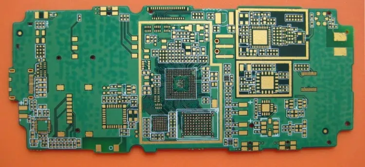
What is Raspberry Pi?

Both autonomous irrigation systems and a robot that can recognize faces can be built with Raspberry Pi’s assistance. We’re experimenting with how it and IoT can work together to create incredible projects.

It enables you to properly handle ordinary computing activities by letting you discover the potential of the cutting-edge computing technologies. Working on different Raspberry Pi ideas might be fun once you took advantage of its versatility. The Raspberry Pi’s adaptability demonstrates the widespread use of IoT.

Raspberry Pi for IoT

It functions as a cost-effective desktop that may serve as a router, video center, or gaming console. Moreover, it can be employed in the creation of robotics, intelligent cameras, smartphones, tablets, and other smart gadgets.

Among the most potent technologies in recent memory is IoT or Internet of Things. Smart switches and autonomous systems are two excellent examples of the IoT applications within practice.

IoT is a new technology which allows people to connect wirelessly with some other devices from a distance. Accessing other devices is simple and affordable when utilizing IoT technology through the use of a Raspberry Pi.

It is simple and affordable to access various devices from distance when using Raspberry Pi and IoT technologies, which may prove quite helpful. This post will show you the proper way to utilize the IoT devices raspberry pi.

As we know, Raspberry Pi was managed by it’s own GPIO pins, so if you intend to create any IoT project, there’s a need to configure those pins and enable the Raspberry Pi’s input and output choices. These pins have been shown to be useful for establishing connections with the IoT devices (these include sensors like light sensors, sound sensors, motion sensors, etc).

How to Utilize The Raspberry Pi for IoT Projects

To quickly and easily explore your imaginations, you can connect IoT with the Raspberry Pi. Heavy IT infrastructure cannot be replaced by Raspberry Pi. Nonetheless, interesting applications include running a low-cost server for website management, examining IP connection, and developing dashboards for the visualization of data making use of Raspberry Pi.

IoT is a developing technology that enables remote wireless communication between users and other equipment. If the IoT technology gets combined with Raspberry Pi, it is affordable and simple to access equipment from distant locations. The Raspberry Pi’s GPIO pins control it. If you want to develop any IoT project, you must configure those pins so as to allow the Raspberry Pi IoT’s output and input possibilities.

These pins make it easier for you to be able to connect to Internet of Things devices that have sensors, such as motion, light, and sound sensors.

Why Do IoT Devices Utilize Raspberry Pi?

FULL PCB MANUFACTURING Quote

In the realm of ambitious tech lovers for computing, Raspberry Pi finally made its way. It is considerably more available to everyone because of its inexpensive cost, enormous processing power on a small board, availability of different interfaces, easily accessible examples plus community support, as well as many other aspects.

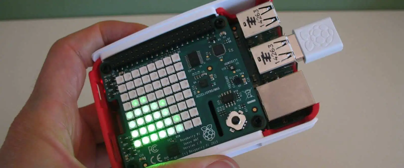
Many RPi models have been made available to date. They all have Broadcom systems on chip with a CPU that is compatible with ARM and the on-chip GPU.

Together with HDMI, a 3.5 mm form of analog audio or video jack, Camera and Digital Serial Interfaces, the Raspberry Pi also has these ports on its board.

Raspbian is among the most widely used operating systems for Raspberry Pi. It is built on Debian operating system and tuned for RPi hardware. Even while the Raspberry Pi has some fascinating capabilities for engineers, it is not suitable for work-related applications. The recent AAC study revealed that almost 20% of respondents admitted utilizing “maker” boards in finished goods. In response to a reader inquiry, some members of the community mentioned employing maker boards, such as Raspberry Pi, inside a variety of contexts, including some instances of professional developments.

Interfacing the RPi to IoT services

Due to its 900 MHz quad-core ARM A7 Processor as well as LPDDR2 SDRAM of 1 GB, the Raspberry Pi can act as the internet gateway. Also, I t is capable of serving as the Internet Gateway Device.

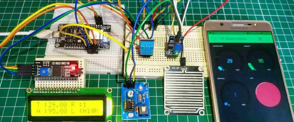
Any IoT project can be made significantly simpler by combining an RPi alongside various commercially available sensors. Many creative minds worldwide pick Raspberry Pi in creating IoT projects because IoT needs a microcontroller for processing data, the Wi-Fi integration for sending that data into the cloud, plus actuators to regulate operations.

IoT Devices Raspberry Pi Devices

IoT Monitoring

Smart Energy Monitors

You can examine how much energy a specific equipment is using with smart energy monitors which are also IoT devices Raspberry Pi. Using this technique, you can keep an eye on the appliances and maybe change their energy usage to reduce additional energy consumption while also helping the environment. Users will need the following supplies to complete this project.

  • Raspberry Pi 4
  • Analog-to-Digital Converter (ADC)
  • AdaFruit.IO
  • Current and voltage sensor devices

Door Lock Using Face Recognition

Facial Recognition technology is now much more important than ever because it offers additional security protection both for homes and workplaces.

Face Recognition can also be described as a AI-based security system that gives you guaranteed level of protection for your home. That resembles the one which you already have on the smartphones. When compared to the other systems on the market, building facial recognition systems with Raspberry Pi is significantly more affordable.

That system is going to be put on the door lock to ensure that anyone attempting to enter your house or place of business will have to successfully pass the facial recognition test. You might control this system while seated in a chair. You will need to purchase these materials in order to complete this project.

Smart Attendance Systems

Smart attendance systems are a fantastic way to use authenticating devices to determine who is present. There are a lot of similar systems on the market, however if you’ve got IoT devices Raspberry Pi, then you should build this system yourself because it won’t start off needing some expensive components and will be reasonably simple to modify. You can also set online interface to make it easier for you to monitor who signs into the attendance system. In that situation, Raspberry Pi would be helpful because you’ll need Python programs to set up the procedure and GPIO pins to build your circuit.

The following items will be needed to complete this project.

Range Extender for Wi-Fi

For those who are interested in electronics communication, the Raspberry Pi ranks among the greatest IoT gadgets. The extender may be used remotely and therefore is automatable because it’s part of the IoT project. You require a Nodemcu ESP8266 in order to complete this project.

This can be described as an IoT application framework with Wi-Fi and some of Arduino’s features. By attaching it to the USB interface, you can utilize the Arduino IDE to program it as needed.

Related Questions

Is the Raspberry Pi Great for IoT?

It’s not necessary for IoT devices to become devices of low-power SoC with the microcontroller serving as the primary CPU as well as the Wi-Fi module serving as a networking interface.

For instance, a typical Computer is capable of functioning as the IoT device, however doing so will be difficult because PCs need hundred of watts for the mains power.

On the contrary, Raspberry Pi is a PC that is a great choice for the IoT processing and is substantially more powerful compared to many other IoT devices. A  Raspberry Pi computer is incredibly small, barely larger than the credit card, yet they consume a small amount of power.

What Does IoT Raspberry Pi Mean?

During recent years, IoT has gained a lot of attention, particularly since the AirTags of Apple were introduced. A network called the IoT links numerous gadgets with data-gathering hardware (like sensors) which may help in sharing data.

To give users the best experience possible, IoT wants to make it feasible for different devices to interact as well as work together. Raspberry Pi circuit boards are well-known single-board computers which are perfectly suited for the DIY IoT device because of their small size and wide features.

Conclusion

Due to its various characteristics, IoT devices Raspberry Pi in a way, has drawn the attention of many people all over the world. Its use also isn’t limited to any one platform because it has developed into a useful tool for building Internet of Things projects. One may consider developing IoT projects which will enhance quality of life, coupled with the projects described above will demonstrate how straightforward it is to do so with a Raspberry Pi which even beginners could create the projects in their homes.

What is Any layer of HDI PCB? Benefits & Applications

hdi pcb design

Many types of PCBs have different layers. You can choose the style that suits your project, such as single-layer circuit boards, multilayer circuit boards, or flexible circuit boards. High-Density Interconnect printed circuit boards are used in electronic appliances & consumer devices because they can fit more elements on a smaller circuit board. 

To make HDI PCBs smaller, advanced technologies are used, such as multiple layers, narrower trace widths, and a via-in-pad layout. These techniques assist in improving signal quality, reducing power usage, and enhancing electrical performance.

What is Any Layer HDI PCB?

HDI PCB has more connections between its layers than a traditional PCB. It means that there are more connections in a smaller area. HDI PCBs also have advanced features like built-up layers, hidden vias, and better signal performance. 

HDI-printed circuit board technology has helped make electronic circuits & devices smaller. An HDI-printed circuit board can have around 160 pins per square inch for more precision. This design allows for dense element placement and versatile routing. Using micro vias, blind vias & buried vias has also helped create denser circuitry. The HDI layer in a PCB uses technology that has become more popular in the industry. This technology allows for more interconnections in a smaller space, so HDI boards are more compact and lighter. The components in HDI printed circuit boards are also closer together, and the vias, openings & copper traces are much smaller compared to traditional PCBs. This denser wiring allows for versatile routing and efficient placement of components. 

In addition, HDI-printed circuit boards have multiple layers that allow manufacturers to do more with less space. HDI PCBs can have many transistors integrated into them, which leads to better performance. The shorter connections in HDI PCBs also help maintain the quality of the electrical signals.ย 

HDI PCBs have tiny holes and thin trace structures. Each layer in an HDI PCB has a high wiring density, allowing for more components to be integrated into a smaller board area. This results in improved performance and signal integrity due to shorter connection distances. 

Difference Between Any Layer HDI PCB and Standard PCB

HDI PCB Board Laminate Structure-Blind Hole Stacking Hole Design-5

HDI PCBs provide better signal quality because they use buried and blind vias to reduce inductance & capacitance. These PCBs have zero stubs, which ensures that the micro via impedance is similar to the trace impedance

Also, a regular hole on a circuit board has more unwanted electric charge around it. This makes it harder to control the flow of electricity. High-density interconnects (HDI) circuit boards are different from regular ones in a few ways. For instance, HDI boards use lasers to make holes instead of machines. Laser drilling is more exact and dependable than rotary drilling. 

Moreover, high-density interconnect (HDI) PCBs can fit more circuits into a smaller space than traditional through-hole circuit boards. Standard boards have fewer components per square inch. Additionally, HDI boards tend to be smaller and lighter, but they still offer more capabilities. Traditional circuit boards are generally bigger and heavier. 

HDI PCBs use advanced techniques like blind vias, micro vias & blind vias, while standard PCBs use through-holes. HDI boards have fewer layers, while standard boards have more. HDI PCBs work well with fine-pitch packages & high pin densities., while traditional through-hole circuit boards can not be suitable for low-pitch packages. 

Furthermore, HDI PCBs are an affordable alternative to standard PCBs. They require fewer layers, which reduces the manufacturing price. The coating interconnections in these boards also improve efficiency, and all the connections on these boards work well. 

Moreover, high-density PCBs provide greater routing density and more dependable connector solutions than standard PCBs. 

 Lamination Process Any Layer HDI PCB

HDI-printed circuit boards are multilayer circuit boards that have densely packed layers. The boards are held together by a lamination process, and the HDI coatings are connected using different kinds of vias. 

To make a high-density circuit board, the process starts by etching the inner copper coating. Then, partially cured layers are separated to reveal the copper coating. The manufacturer then stacks these layers with  

 prepreg material on the top and bottom. Finally, the manufacturer utilizes high pressure and temperature to press the stack together. The temperature should be very high to melt the prepreg and form a solid layer. This process creates what’s called an HDI layer. 

After the high-temperature process, the melted prepregs cool down and join the layers. To make an HDI PCB, the layers need to go through multiple laminations. The more lamination there is, the more expensive the PCB will be. Designers can also add more coatings to increase the routing density, and sequential lamination helps create intricate designs. 

The layering methods used in HDI PCBs can be customized according to the design needs. Here are some of the commonly used kinds of HDI stack-ups. 

ยท 1+N+1

This stack-up for a printed circuit board includes only one HDI layer. It is well-suited for ball grid array (BGA) components with fewer input/output connections. This stack type is also suitable for mobile devices such as cell phones.

ยท 2+N+2

This HDI stack-up is more complicated than the previous one, as it has multiple build-ups of HDI layers. It is particularly suitable for BGA components with many input/output connections. This stack provides superior layer interconnection compared to the more straightforward stack-up. 

ยท Any layer HDI

Every layer in this type of stack-up consists of HDI layers. In addition, any layer high-density interconnection design allows for the connection of the conductors on the HDI layer using copper-filled micro vias.

Benefits of Any Layer HDI PCB Boards

HDI PCB Board Laminate Structure-2

Nowadays, televisions, computers, and other electronic applications are no longer bulky or heavy. 

 Moreover, these appliances are now designed to be compact and stylish. Electronic devices have become an integral part of human life and define how we live in many ways. Modern electronic appliances are designed with compactness in mind, and using HDI-printed circuit boards provides several benefits. :

ยท Enhanced signal integrity

HDI boards incorporate technologies such as blind vias & via-in-pad, which enable manufacturers to place components closer to each other, thereby reducing signal track length. HDI printed circuit board technology eliminates via stubs, minimizing signal reflection, which increases signal quality. 

ยท Cost-effective

HDI PCBs are an affordable choice for advanced devices and provide more functionality than standard circuit boards. For example, a 6-layer HDI circuit board can offer the same functionality as an 8-layer standard PCB. Manufacturing costs for HDI boards are lower as they require fewer layers than traditional boards. 

ยท Better reliability

HDI boards provide higher reliability than conventional PCBs. Microvias are tiny holes in circuit boards that are better at staying solid and reliable than bigger holes called through holes. Because they are small, they work better on high-density circuit boards and can be a dependable choice.

ยท Space saving

HDI boards are unique circuit boards with more minor and closely packed connections. This makes them take up less space and helps make the boards smaller overall. Additionally, using buried vias, micro vias & blind vias decreases the board’s space requirements. 

ยท Faster time-to-market

The layout efficiencies of HDI printed circuit boards enable faster time-to-market, and the testing & design procedure for HDI printed circuit boards takes less time than traditional PCBs. This is due to the ease of components and placement on the board. 

Applications of Any Layer HDI PCB Boards

FULL PCB MANUFACTURING Quote

HDI-printed circuit boards are frequently used in sophisticated devices that demand high performance. These PCBs find application in various devices such as laptops, smartphones, medical equipment & military devices. 

ยท Medical devices

HDI PCBs play a critical role in the healthcare industry, with many modern medical appliances incorporating them. Advanced medical equipment such as surgical instruments, imaging devices, & laboratory analysis equipment utilizes HDI PCBs. For example, miniaturized cameras that provide high-quality images of internal organs and tissues are now possible due to HDI PCBs. 

ยท Wearable technology

HDI boards are used in wearable devices such as smartwatches and VR headsets, which are becoming increasingly famous among young people. These boards enable the production of compact and intricate machines. HDI PCBs are also commonly found in handheld & mobile devices. 

ยท Automotive industry

HDI PCBs are proving useful in the car industry, where reducing weight can improve performance. With modern cars becoming more connected and computerized, HDI PCBs are essential for operation. Today’s automobiles have about 50 microprocessors for engine controls, safety features, and diagnostics. HDI PCBs are integrated into advanced features such as rearview cameras, onboard WiFi & GPS, and backup sensors. 

ยท Military and aerospace

HDI PCBs are well-suited for military & aerospace devices that operate in extreme environments. Some electronic devices need to work well, even in dangerous conditions. HDI circuit boards can help these devices work their best, even when risky or unsafe. 

ยท Industrial equipment

IoT devices are increasingly prevalent in industrial settings such as warehousing and manufacturing, and many incorporate HDI technology. Electronic tools are commonly employed by businesses to track inventory and monitor equipment performanceโ€”industrial machines often contain smart sensors that gather data & connect with appliances via the internet. HDI circuit boards are frequently utilized in the manufacture of such devices. 

Conclusion

HDI circuit boards have a lot of good things about them, like more connections that can help the board work better. They can also make electronic devices smaller, which is helpful for many devices. Some of these boards also have a special coating that helps them work even better.

Top Benefits and Applications of Ultra-Thin Flexible PCB

Flexible pcb board cost

Smaller copper characteristics and some other board materials are used on ultra-thin flex PCBs that are very thin. These devices lack the stiffness of regular circuit boards and are incredibly lightweight.

Demand for ultra-thin flexible PCBs is increasing along with the demand for increasingly more miniature devices. Compact devices for mobile, wearables, implantable, and other tiny devices must be developed with PCBs.

The Benefits of Ultra-Thin Flexible PCBs

In addition to their size, ultra-thin flexible PCBs provide a number of benefits. For your gadget, using a flexible PCB secures a number of advantages:

  1. Reduce material costs: PCBs contain components of pricey components like copper. Thinner boards have cheaper material costs since they use fewer of those components. This decrease equalizes production and handling costs.
  2. Compatibility with cutting-edge methods: Ultra-thin PCBs may be used with cutting-edge methods such as direct laser imaging. These methods can be employed with caution and exact registration procedures without causing harm to the flex PCB.
  3. Dependability: Custom repeating routing pathways can be hosted on an extra-thin circuit board. You’ll experience low service calls because of the greater dependability that each flex board brings.
  4. Improved defense: These Boards feature polyimide coverings on the conductors. This dielectric layer, along with other cover and base materials, provides defense against a number of potentially dangerous circumstances.
  5. Low mass and high ductility: These characteristics lessen stress and impact on the solder joints and flex boards. Low mass and excellent ductility assist the flex PCB in tolerating harsh operating circumstances since acceleration and vibration are particularly difficult for such joints.
  6. Robustness: Ultra-thin Printed Circuit Boards can withstand many flexing cycles. A PCB preserves the integrity of both materials by acting as a transitional element between flexible and stiff sections.

Material For Ultra-Thin Flexible PCBs

flexible printed circuit

A new level of PCB miniaturization is made feasible by thin base substances. While shrinking PCBs in the direction of Z results in a thinner board and more room for components, shrinking circuit boards in the Y and X dimensions just decrease their footprint.

  1. Copper layers: Flex PCB connections require less plated copper than rigid PCB connectors. The connector footprint is lower because of such thin layers of copper. Moreover, thinner layers produce lines and spaces with little resolution.
  2. Polyimide: Coatings and layers constructed of polyimide offer additional security without bulking up the electronic circuit.
  3. Adhesive: To join and attach various bending pieces so they can tolerate flexing, layers of high-quality glue are used.

For small devices like hearing aids and medical implants, flexible ultra-thin substrates are necessary. The size of all these components affects patient comfort because thin substrates flex more easily. Flat substrates have to possess the flexibility to fold and bend without harming the circuit board in order to minimize their size.

Ultra-Thin Flexible PCB Application

Extra-thin PCBs are perfect for uses where it is hard to utilize other types of PCBs. Designers often choose a flexible PCB because of its distinct benefits over wires and conventional PCB design. Flex PCBs may be bent to fit any area or package while exhibiting the same uniformity, density, and accuracy as rigid PCBs.

Flex circuits are found in drawing boards, SIM cards, metro coins, and implantable and wearable medical devices.

Replace wiring harnesses with flex circuits for one of their most popular uses. Many hardboards, wires, and connections can be replaced with a single flex PCB.

By eliminating the need to color-code and bundle wires during assembly, applying these kinds of boards can save both labor and supplies. There are three significant benefits to streamlining this procedure:

Faster production rates, lower installation expenses, and fewer assembly- and service-related issues

A flex board can take the place of wire harnesses to increase the repeatability of wiring routing, and by removing mistakes, test durations, repairs, and rejections are reduced. Moreover, flat strip conductors may carry a greater current than circular wires and are better at dissipating heat. Stronger relationships are produced by these traits. A designer has more control over impedance, noise, and crosstalk after they decide on a consistent conductor arrangement for the flexible PCB.

Types Of Ultra-Thin PCBs

FULL PCB MANUFACTURING Quote

Two main varieties of long, thin Printed Circuit Boards are available. These are ultra-thin flex PCB and rigid PCB.

ยท Rigid Ultra-Thin PCB:

For applications that need a 2D PCB, stiff ultra-thin PCB materials are readily available. Typically, you may use them as a substrate for packing ICs, or integrated circuits. Here, they assist in making the component as a whole incredibly thin.

You may find 25-micron lines as well as broad gaps, 175-micron or smaller pitches, and 50 and 100-micron vias and pads here.

ยท Ultra-Thin Flexible PCB:

Also known as super thin flexible PCB. Often, flexible laminates are used to create this long, thin Board. The PCB might collapse as a result. As a result, less space is needed to store or encapsulate the board on both a surface area and volume level. The density of integration rises as a result.

Additionally, superior bending is made simple by the ultra-thin Circuit. The manufacture of cables that need dynamic bending is one use for ultra-thin flex PCBs. This is a result of their strong bending abilities.

Single-Sided Ultra-Thin PCB Vs. Double-Sided Ultra-Thin PCB: Whatโ€™s The Difference?

Conducive copper is used on the single-layered, ultra-thin Circuit, and components are put on each of the sides of the board. It also features conductive wire on the opposite surface. This is the only kind of long, thin PCB that is commonly manufactured. This is due to their fundamental character and simplicity.

Single-layered PCBs are frequently used in a variety of devices, such as radio equipment, printers, calculators, camera systems, and more.

Contrarily, double-layered ultra-thin Circuits have traces on both sides with a bottom and top layer. Any surface of the board may be simply fitted with active copper and electrical components. This makes it possible for the traces to pass through one another. The end product is high-density circuitry that doesn’t require soldering.

The fabrication of double-sided extremely thin PCBs may be more difficult since they are more complex than their single-sided equivalents. Nonetheless, the advantages of double-layered, ultra-thin PCBs outweigh their drawbacks by a wide margin.

The most popular variety of double-layered ultra-thin PCBs is the latter. This is so that highly complex boards may be produced with their assistance. This is advantageous for PCB purposes as well as devices involving advanced electronics.

Double-layered long thin Circuits are used in a variety of devices, including vending machines, lighting systems, amplifiers, and automotive dashboards.

Drill Microvias Into Ultra-Thin PCB

fpc-pcb

For drilling micro vias onto extremely thin PCBs, there are many methods that exist. They consist of plasma etching, laser drilling, and photo-via drilling. Let’s examine each of these methods in turn.

ยท Photo-via Drilling:

Photo-imaginable dielectric material and lithographic patterning are used in photo-via equipment. The development of the ultra-thin HDI Circuit has been made possible by this technology. Additionally, the hole’s size is around 25 m in both depth and diameter. Also, the dielectric substance used in this drilling technique makes it pricey.

ยท Plasma Etching:

Using plasma, this micro via-drilling technique etches the PCB material to create holes. With this method, it is possible to create a via house with a 75 mm diameter out of substances that are about 25 mm thick.

Yet, this approach is the least expensive for digging the via compared to other expenditures associated with vacuum equipment.

ยท Laser Drilling:

The most intriguing of all is this drilling technique. For dielectric materials with a thickness of 5 m, you may use this approach to increase the diameter of the vias up to 5 m.

The wavelength, thickness of substrate material, substrate type, and density of energy are the main driving forces behind such a micro via drilling process.

The best technique for micro vias, typically involving concentrating the laser light on an extremely small region, is this one. The vias that are produced are equally as clean as those made by mechanical drilling. By doing this, it is ensured that the plating is applied uniformly to the inside of the vias.

In contrast to mechanical drilling, this approach has a slower drill speed. Using any wavelength between ultraviolet and far-infrared, you may use this technology to easily drill the thick micro vias inside an ultra-thin Circuit.

However, this method has a drawback. This is due to the laser beam’s restricted depth, which can be drilled with consistency and dependability. The maximum depth a laser can dig is constrained when just one lens is used for beam concentration. This is a result of the limited depth of focus.

Yet, a collimated laser beam guarantees that the laser, via the form of drilling, reaches a significantly greater depth. The via’s extremely small size, which results in the Fresnel diffraction of the beam, is a problem in this case. This, in turn, may have an effect on the beam’s intensity in extremely deep micro via holes.

Conclusion

We believe we have covered all the necessary information regarding ultra-thin Printed Circuit Boards. As has been mentioned, this form of PCB is thinner than the normal one. Moreover, it provides less weight and is more compact. This is a result of the board’s materials being used less.

Many PCB manufacturers provide you with the finest by providing you with customized ultra-thin Circuits based on what your particular demands are. For affordable rates and high-performance solutions for the ultra-thin PCB, contact RayPCB now.

Why choose the RayPcb as your 24-hour PCB manufacturer?

nanya pcb

RayPCB.com is a company that can quickly make printed circuit boards (PCBs) for research projects. They can make the PCBs and assemble them in just 72 hours if you need them fast. RayMing Technology is a one-stop shop for all your manufacturing and PCB assembly needs. They provide best-quality services that can be customized according to your specifications. 

24 Hour PCB Manufacturer

At RayMing, being fast is essential in today’s business world. We specialize in quick-turn printed circuit board fabrication and assembly services. Our skilled manufacturing team is dedicated to meeting your needs for NPI, printed circuit board Prototyping and Bread Boarding. We are committed to doing everything we can to provide high-quality service.ย 

If you need an electronic project to be done fastly, choose RayMing.

We can make PCBs fast enough to meet your tight deadlines. We also have processes to ensure your printed circuit board order is handled quickly from the beginning to the end, from giving you a price estimate to delivering the finished boards. We do everything in-house and don’t outsource any part of our quick process, so you can trust us to have your PCBs quickly and with high quality. Our swift turn service is available for all clients, including those who need certification for industry, defense, and automotive products. 

We make quick-turn PCBs very fast, but we still maintain the same high-quality standards that our customers expect from us at RayMing. 

  1. We can manufacture PCBs (single-sided, double-sided, and 4-layer) in 24 hours. 
  2. We use digital systems to quickly provide quotes, process orders, design and manufacture PCBs, test them, and ship them.
  3. All standard processing of PCB steps are completed in-house at our fabrication facility
  4. We have complete control over the PCB manufacturing process, ensuring timely completion and high-quality products. 


Consider a 24 Hour PCB Manufacturer

Shengyi WLM1 PCB

Quick PCB assembly manufacturing is becoming increasingly popular and essential for the electronics industry. This market is expected to grow from 54.3 billion dollars to 58.87 billion dollars from 2021 to 2022, according to market statistics. 

Some clients have been unhappy with their printed circuit board assembly companies because their staff did not meet the deadlines. This article can help you learn about fast-turn printed circuit board assembly to avoid such situations.

What Is 24 Hour PCB Manufacturer?

Quick-turn printed circuit board assembly means making a PCB concisely, usually within 24_48 hours, while maintaining quality & precision. 

To make sure the PCB is assembled correctly, the manufacturer needs to check things like design, layers, and mounting methods. Quick-turn printed circuit board fabrication is designed to speed up the process of designing, manufacturing, and assembling the PCB. It’s also a good idea to make a prototype of the PCB to test it before making many of them sell.  

Benefits Of 24 Hour PCB Manufacturer

The electronics industry is very competitive, and being the first to introduce a new product can give a company an advantage. One way to get to the market quickly is by using fast PCB (printed circuit board) assembly services. These services offer several benefits, such as getting your product to market faster

  1. Turnaround Time: Fast PCB assembly services mean that clients can get their boards assembled quickly, even for complex circuits. The excellent producer ensures clients are happy with how quickly they get their circuit boards. However, if manufacturers promise to deliver the circuit boards speedily but end up taking too long, clients may lose trust, and it can delay their product getting to market. 
  2. Cost Saving: The “Quick turn printed circuit board assembly package” is a helpful way for manufacturers to save money and time in making circuit boards. This process also includes testing the circuit boards using good equipment, which is a cheap and effective way to check if they work properly
  3. Different Boards: Manufacturers want to make their clients happy, so they give them options for different types of circuit boards to choose from. It lets designers try various circuit boards to see which works best. The producer offers both expensive and sturdy boards at reasonable prices. 

Procedure of 24 Hour PCB Manufacturer

FULL PCB MANUFACTURING Quote

When a designer wants a quote from a printed circuit board assembly company, they usually propel a Gerber file. The company will review the file and make sure they understand the layout. Then they will send a file back to the designer for approval. Once the designer approves the file, the process of making the circuit board can begin. 

ยท PCB Prototyping

The “quick turn PCB” is the first step in making circuit boards. It lets designers test their ideas before making the final product. When designers send Gerber files, they may not have finished their designs. So, they use jumpers to check (test) the circuit boards.

ยท Assembly Stage

Once the designer has tested their circuit board using the “fast turn PCB” process and is satisfied with its appearance, the next step is “component assembly.” During this stage, the printed circuit board assembly services might use “hot air solder leveling” or “ball grid array soldering” on flexible circuit boards. 

ยท THA

In THA, the people in charge put and attach components with metal legs through the holes in the circuit board. They then heat to melt a unique metal that sticks the parts to the board. 

  • Combined Assembly

The fast PCB maker uses both surface-mount technology and thru-hole assembly techniques to put the circuit board together. It is a popular method used by many assembly services. Once the board is put together and checked, it is wrapped up and sent to the customer. 

Decide The Cost Of 24 Hour PCB Manufacturer Services

It’s essential to understand what makes the price of printed circuit board assembly services go up or down. It helps designers to know what to expect. Here are some of the things that affect the cost. 

  • Quantity: The cost of making PCBs quickly can be affected by how many boards are needed. The price can also change depending on how many layers each panel has. 
  • Machine Cost: When making PCBs quickly, there need to be technicians & engineers available right away. They have to be able to work faster than before. Also, the machines used to put the PCBs together can be different for each board
  • Assembly: As we said before, there are many ways to assemble circuit boards, like SMT, THA & Mixed technology. Each of these methods has a different cost. But, most companies that make PCBs like to use a mix of these technologies. 
  • Quick Time: When manufacturers offer fast turn services, they must work hard to deliver products on time. They may have to work around the clock and put in the extra effort. The price of this fast delivery relies on how quickly the product needs to be made
  • Packaging & Delivery: Everyone knows that packaging & delivery are just as essential as making the PCB. So, if someone wants a quick-turn printed circuit board assembly, they must be ready to spend a lot of money on delivering and packaging the PCB correctly. 

Factors When Selecting 24 Hour PCB Manufacturer

  • Experience: Designers don’t want to waste valuable resources on any bad printed circuit board assembly team. That’s why it’s a good idea for them to ask about the assembly team’s experience and methods before hiring them. 
  • Delivery Time: Make sure you know when you will get your PCBs delivered, and also have a contract in case they break their promise. Also, check if their turnaround time is possible. 
  • Quality: Ensure the urn PCB assembly services use products that meet international standards without sacrificing quality.
  • Price: If you want to check if the price for a quick-turn printed circuit board assembly service in the USA is reasonable, ask for quotes from different companies. It will help you know what is expected in the industry.

Final Thoughts

Because the printed circuit board market is expected to grow, it’s an intelligent decision for designers to use quick-turn printed circuit board assembly services. These turnkey PCB assemblies can provide designers with a lot of time to work on new ideas and designs and can also help them save money

What Is Multilayer Fr4 PCB Substrate Material?

multilayer pcb manufacturers

FR4 serves as a name and a reference rating, &  it is also written as FR-4. For high-quality PCB manufacturing operations, FR4 is the perfect default substrate material because of these characteristics. These characteristics can also serve as the basis for PCBs that are both high-quality and affordable when employed properly.

FR4 serves as the main insulating backbone of a PCB. This serves as the foundation upon which the circuit is built by the manufacturer. The FR4 board is prepared and then heated and coated with one or many folds of copper foil applying adhesive. Depending on the board’s design, this copper may wrap one or either side and create the connectors in the final version.

To create more complex circuitry, complex PCBs may layer the electronic circuit or use more than one side. From here, the board is prepared for the last touchscreen layer and the following soldering process by having the circuits designed and filed off before being coated with a modified surface layer.

Ceramic vs. FR4 PCB : When to Use?

multilayer pcb manufacturing

When most people hear the phrase “ceramics,” they immediately think of their primary or secondary school art class when they proudly made their parents a misshapen coffee cup. When you were an engineer, ceramic materials were essential to the creation of electronic components. Knowing how to design a different substrate PCB with transistors can be helpful.

Ceramic PCBs are advantageous for industries that need faster-speed amplitude boards that can survive challenging environments. By transitioning from FR4 to ceramic Boards, heavy industrial and aerospace equipment can experience significant improvements in reliability. The main disadvantage is the price, which can add up in large manufacturing runs.

ยท Ceramic vs. Multilayer FR4 PCB 

Compared to FR4 boards, ceramic boards have several unique features that can be used in specific applications. There is no one “ceramic” substance; rather, the term applies to a class of substances that share a similar chemical makeup and set of physical characteristics. Aluminum oxide, aluminum nitride, and beryllium oxide are ceramic materials utilized as substrates for circuit boards. Other ceramics with comparable properties include those made from substrates like silicon carbide and boron nitride.

The heat conductivity of FR4 and porcelain materials is a significant distinction. Comparatively to the ceramic materials employed for a circuit, FR4 has an appallingly low thermal conductivity. FR4 is roughly 20 times more thermally conductive than aluminum oxide. Beryllium oxide always has greater thermal conductivity than aluminum nitride, which is around 100 times more thermally conductive than silicon carbide. The material with the greatest thermal conductivity is boron nitride.

High thermal demands on FR4 Boards frequently need the use of metal structures to convey heat in order to make up for their poor thermal conductivity. Heat is transferred away from the surface layers through thermal connectors, metal surfaces on the inner surface, active cooling components like blowers, and thermal landings. Except for extreme circumstances, porcelain boards do not need these components, and heat can be simply transferred to a mechanical landing, an effective cooling feature, or device packaging.

Chemistry and physics majors may be aware that materials that carry heat well also make excellent electrical conductors. Ceramics defy this tendency a little. Thus these boards can still be utilized as PCB substrates because their conductivity is so low. Doping, which is also how ceramic resistors’ resistance is set, can be used to change the electrical properties of ceramic boards.

ยท Multilayer FR4 PCB Ceramic Boards

FULL PCB MANUFACTURING Quote

Further advantages of ceramic boards make them particularly beneficial for multilayer boards. Due to more consistent heat transport across the board, the high degree of thermal conductivity helps minimize the development of critical areas on the base and inner circuit layers. Heat waves are more prone to emerge on an FR4 PCB because it depends on metallic structures or aggressive cooling to move heat away from specific areas of the circuit or between layers.

Vias on FR4 boards are prone to fracture during temperature cycling and are used by multilayer boards to access the interior layers of a circuit. Deficiencies in the thermal expansion ratio between copper and FR4 cause the possibility of fracture to exist. These boards experience stress from thermal cycling along the chamber and butt connections within vias. Designers must take additional precautions to prevent failure since these spots are prone to fracture.

Because the thermal expansion coefficients of ceramic circuit boards are closer to those of their conductor structures, less stress builds up during thermal cycling in these structures. The ceramic board’s better overall thermal conductivity guarantees that heat capacity is also more consistent, preventing significant stress from being placed on any vias in a specific area of the board.

Ceramics possess a desirable level of mechanical strength and are capable of withstanding high mechanical loads, such as powerful vibrations and shock. A porcelain board will often distort less than an FR4 for just that applied stress since they have smaller Young’s moduli.

ยท Manufacturing Multilayer FR4 PCB Ceramic Boards

Silver or gold conductive pastes can be used throughout the ceramic board manufacturing process to lay trace connections in each layer. A coat screen printing procedure is commonly used to insert these metal components or substrates in each layer. Furthermore, micro vias can be laser-drilled or physically hammered in an unfired layer.

The complete stack of printed and stacked ceramic layers is then baked in an oven. The ceramic board must be baked at a temperature below 1000 ยฐC, which is the same as the temperature at which gold and silver paste sinter. Gold and silver can be used on ceramic Boards thanks to this cooling bake method.

It is simple to incorporate analog elements directly into the inner layers of a ceramic PCB thanks to the compression molding and sintering process for multilayer PCBs. In a PCB constructed of FR4 material, this is not feasible. Designers are now able to enhance the density of connections and components on inner layers.

How To Select Multilayer Fr4 PCB Thickness?

multilayer circuit board

The designer or electrical engineer should specify the FR4 thickness when placing an order for a laminate board for a PCB project. Based on which is most suitable for the environment, this is determined in inch-based quantities, like a 1,000th of an inch, thou, or millimeters. FR4 sheets can be any thickness. However, they often span from ten through to three inches depending on the project’s requirements.

Although board thickness might not appear to be a crucial element in a PCB’s design, it actually is. In order to determine the width of a plank for design, numerous criteria are taken into account because board thickness impacts a number of the board’s functional characteristics. The following are some of them.

1. Space

If the designer is concerned about space, a smaller FR4 board is typically preferred. This is a key component in the creation of numerous Bluetooth accessories and USB connectors, which are tiny devices. Smaller FR4 PCBs are typically preferred to reduce space inside the device, even for bigger applications.

2. Connections:

An edge connector is necessary to link the two sides of a two-sided PCB design. Since PCB edge connectors can only fit a specific range of PCB thicknesses, this might be a significant limiting factor for the PCB’s final size. To avoid slippage or PCB damage, a connector’s mating component must fit tightly against the edge of the Board. That’s one of the main explanations for why choosing the material for the circuit comes before designing the circuit.

3. Impedance Matching

Each multi-layered board serves as a capacitor for the layers below it. Because the width of the PCB FR4 substance impacts the width of the insulator, which significantly influences the capacitance value, the width of this panel is crucial.

This is a particularly important consideration for some elevated PCB designs, such as Rf/microwave ones. Getting the proper inductance for every layer is vital in high-frequency designs because impedance matching is a crucial element for maintaining good board performance. 

Who are the Best Electronics Suppliers in China?

EMS Electronics Manufacturing Companies

With a purposeful focus on enhancing their products’ quality rather than merely the quantity, the electronic suppliers in China has made a substantial contribution towards our global economy over the past few years. With exports of more than $20,747.10 million in 2017, China’s wholesale market for technology achieved a record high and is predicted to rise much further in years to come.

You won’t feel deflated or defeated any longer whenever you see “made in China” on your electronic devices. Below are the best electronics suppliers in China, who offer high-end products at surprisingly inexpensive costs.

Before we explain further on the best electronics suppliers in China, let us first consider who an electronics supplier is.

Who is an Electronics Supplier?

Electronic suppliers play a crucial role in supply chain that provides manufacturers of electronic equipment with components they need, including surface mount component, leaded components, and different types of semiconductor devices

Getting the correct components in place at proper time is essential for an effective operation since supply could be a hard process.

Distributors were organized to manage the delivery of various components from various manufacturers into a wide number of organizations, but component producers lack the ability of interfering with many businesses, both large and small.

Best Electronics Suppliers in China

China has seen the emergence of a number of electronic manufacturing enterprises over the past several years, and you can now image the abrupt acceleration in the GDP.

Well, the influence of the wholesale electronics business to the economy is always positive.

You may digitally connect to some of the most well-known electronics suppliers in China’s B2B marketplace to buy genuine goods. These Chinese electronic suppliers listed below are among the most reputable and verified, allowing you to invest there without worrying that luck would go against you.

Huaqiang Electronic World

One of China’s biggest markets for consumer electronics is Huaqiang Electronic World. You’ll undoubtedly find whatever you require here, as there are six stories here featuring almost every form of electrical device you can imagine. They even feature some cutting-edge, environmentally friendly technologies; such fully recycled cardboard lamps and chairs.

Due to its most reliable electronic products being offered at wholesale costs, Huaqiang Electronic World is capturing the whole country’s hearts of China. The manufacturers’ interiors are highly opulent, and they creatively display their products there to attract customers. Their whole product line has captured the interest of consumers, and both international and domestic markets are experiencing extremely high demand.

Linbova Technology Co. Ltd

Linbova Technology Co. Ltd seems to be the best place to go if you’re seeking for some high-tech tools as well as electronics at a great price. With the promotion of the high-end products in competitive markets, electronics suppliers in China have taken the lead in the industry. Additionally, the business specializes in products that may be customized and is especially targeted at technical specialists that use these products in their line of work.

Dongguan Sen Dong Electronics

FULL PCB MANUFACTURING Quote

This electronics supplier in China was established in 2003. By consistently expanding the product lineup that is now within the grasp of consumers, manufacturers have contributed to economic progress. This company is known as ISO 9000 certified, which is the strongest argument in favor of it.

While having a limited selection of products, it handles a spectrum of tech-related electronic items, peripherals, and products. This electronics supplier in China must be visited if you’re looking for inexpensive electronic products.

Shenzhen Saiqiao Technology Ltd

Though not too old, its products are valuable investments. Soon just after founding in 2013, the business gained notoriety for manufacturing high-demand wholesale electronic products. It offers a variety of goods at very low costs, includes USB cables, audio cables, HDMI cables, chargers, as well as other types of mobile accessories. Due to their true commitment to placing quality before quantity, an ISO-certified organization can be relied upon for both their products and judgments.

Marvel Electronics Shenzhen Co.

Another reputable brand that handles the efficient and top-notch goods sector of the electronic industry of China. The majority of foreign customers place orders with the business in order to acquire flawless and unrivaled products. The business is well known for making premium LCD modules. Several of its prospective customers are in North America, Europe, East Africa, and Australia, whereby electronic suppliers can export their goods.

Shenzhen Hosing Technological Development

This high technological company specializes in making USB cables, power banks, as well as phone and automobile chargers. Mobile chargers for phones, cameras, and other digital equipment are made of power banks.

They provide a great deal of product versatility in terms of capacity, interoperability, design, and clever safety features. Regarding manufacturing and designing, they operate under the ISO 9001 standard, which is an established system for quality management on a global scaleIts market has expanded to many other parts of the world, including North America, Middle East, and Europe.

Shenzhen Linbova Technologies

A smaller business called Shenzhen Linbova Technologies focuses on making bluetooth speakers, outdoor devices, and game controllers.

This 2017-founded company outperforms its competitors by employing research as well as development engineers that will adapt any product from their inventory to your demands. Also, this business has an ISO-9001 management certificate, as well as the manufacturing process is carefully monitored by trained professionals.

B&K Electronic Technologies

Consumer Electronics Assembly

With just nine employees, trade company B&K Electronic Technologies, which was founded in 2017, is a relative newcomer in a very cutthroat industry. They produce technological devices like wireless phone charger, bluetooth devices, and a variety of phone cases.

Every employee has more than a decade years of business experience and has worked with some innovative tech businesses of modern time, including Apple, Huawei, and Samsung, to bring products to market.

Guangzhou YOUTOP Digital Science Technologies

This electronics supplier in China is dedicated to creating, designing, as well as producing personalized digital gifts to serve commercially-oriented marketing campaigns. This business, which was founded in 2004, will consult with you extensively to identify the ideal product for your requirements. Its staff members are very knowledgeable about development and research and constantly strive to create the most modern technologies.

They have collaborated with a number of well-known businesses worldwide, and their goods are well-liked on all international markets. Also, each product complies with current health standards including RoHS, C3, and CE.

Flying Communication Ltd

Flying Communication Company was founded in 2004 renowned for providing different phone cases, including hybrid cases, waterproof cases, and earphone cases, as well as screen protectors.

Their typical yearly sales range from $200 million to around $500 million. They don’t make electrical devices themselves, but for the last fourteen years, they have been the top choice for phone cases.

Dongguan Sen Dong Electronics

Since its founding in 2003, this company has been engaged in the production, development, and research of mobile devices and related accessories, particularly earphones. This business has ISO 9000 accreditation, which is superior than ISO 9001 certification in that it covers all areas of the quality management systems as opposed to just one.

Shenzhen Marvel Electronics Ltd

The 2012 establishment of Marvel Electronic is dedicated to the production of LCD modules, including alphanumeric, dot-matrix, animated graphics, dot-matrix, as well as TFT LCDs.

In addition, they manufacture products including computer speakers, optical cables, ABS phone casings, LED panel light, specially made USB flash drive, phones, tablets, and Android devices. This business offers its services to customers in Australia, Europe, Africa, Middle East, as well as North America at very affordable costs.

Shenzhen Saiqiao Technology Ltd

Electronics Assembly Companies

This manufacturing company was founded in 2013 that produces digital goods, accessories for mobile phones, and electronic presents. They produce a variety of goods, including chargers, Samsung and iPhone accessories, HDMI cables, audio cables, and USB cables.

 The business appreciates its reputation with clients and is certified under ISO 9000 as well as EICC. It also offers cheap prices, prompt delivery, and excellent service. They employ approximately 100 people and offer free product samples, and provide about 10000 pieces daily.

Dongguan Harbour Technology

Headphones, phone cords, smart watches, and car chargers are all offered by this electronics suppliuer in China.. Saudi Arabia and the United States are where they get most of their business. Despite their recent existence, they are an ISO 9001 as well as 14001 certified diamond member for made-in-china.com.

It’s crucial to assure fast payment to China manufacturers and suppliers when purchasing products made in China. This guarantees that your order will be shipped promptly and that the agreed-upon prices will not change.

Rantle East Electronic Limited

This is another leading Chinese suppliers of electronic components; a  full-service independent distributor of the different electronic components, has been in business since 2003. For OEMs, Service and Repair, as well as Contract Manufacturers, Distributors, Research and development Groups, as well as other businesses that need electronic components, our company offer a comprehensive and affordable sourcing solution.

Also, aside from having a huge choice and selection of components in store, we also provide free sourcing of components for our clients. By combining our online search engine, that collects information both our warehouse stock and the worldwide stock available via our Reliable Supplier Network, with collection of millions of data files out of the major OEMs as well as stockists, we quickly and effectively find both obsolete and current parts.

Win Source Electronics

You are fully aware of how challenging it is to find old electronic parts. Purchasing should always take around 60% of a buyer’s time, which is twice as much time as discovering typical parts.

In response to this problem, WIN SOURCE continuously improves their in-stock inventory as well as a worldwide supplier network to shorten customer procurement cycles, decrease transaction costs, as well as offer high-quality electronic components for affordable prices.

How Do I Pick Electronics Suppliers in China?

Choosing the best and most reliable electrical manufacturing services provider could prove very difficult, particularly in Asia. This is due to the fact that there are lots of them available and selecting one over another may be difficult. Also, due to their abundance, some individuals could find up teaming up with an incorrect provider of electronic manufacturing service. But, you can use the guidelines listed below to stop the occurrence of this.

Before contacting an electrical manufacturing services provider, you must first take into account their rating. The majority of variables and labor influence a company’s ranking. For instance, the ranking of a provider of the electronics supplier in China takes into account manufacturing expertise, scale, and capacity inside the technology, sector, sector certifications, etc.

High ratings indicate a high probability of high-quality product manufacturing for the provider of the electronic manufacturing services. This also applies to exceedingly low ratings. Also, if a firm seems to have no ratings, you should do extra research on it in addition to using other criteria to determine whether it is good fit for all your personal manufacturing needs.

Examine your electronic manufacturing service provider’s internet reviews. Most internet reviewers typically take certain factors into account. Also, they are frequently new or long-time users or clients of the provider of the electronic manufacturing service. That is why customers’ reviews of their interactions with the manufacturer’s goods and services function as an extremely important barometer of the caliber and capability of production from the supplier of the electronic manufacturing services.

In order to assess a supplier’s suitability and capability for your manufacturing requirements, you need also consider other areas of the supplier’s electronic manufacturing service.

Conclusion

One cannot overstate the importance of selecting the appropriate provider of electronic manufacturing service for the electronic needs of companies in Asia. Even if the procedure could be challenging, you simply cannot skip it.

Furthermore, we have provided some recommendations to help you choose wisely. We’ve also provided advice regarding how to pick the best electronics suppliers in China for your requirements. You can contact us here whenever you have further inquiries. We are always available to meet your needs.

Who is a Hardware Development Engineer?

hardware development engineer

The Hardware Development Engineer is someone who develops hardware, and is involved in designing, producing, installing, and upgrading hardware components.  Computer mouse, modems, keyboards, disk drives, circuit boards, as well as other devices are examples of hardware components.

The hardware development engineer will create and produce new prototypes in addition to modifying hardware. You also will supervise the fabrication of new parts and make sure that it follows the previously created pattern. To assess the new items’ functionality, you should test them. Another obligation has to do with assessing the compatibility of new hardware with old software.

Also, the minimum educational prerequisite is a Bachelor of Science degree in electronics, computer programming, engineering, or equivalent subjects. You must also have excellent problem-solving and decision-making abilities, coupled with strong analytical and critical skills for this position.

You ought to be capable of concentrating on details, use deductive reasoning, and be quite imaginative.

What Does Hardware Development Mean?

hardware development

Hardware development involves a complex undertaking that comprises the optimization and creation of the mechanical and electronic system elements which conduct various computational functions. Typically, the hardware interface is used to realize the connection in between objects and elements.

Typically, hardware development involves the following phases:

  • creation of hardware element schematics;
  • implementation of hardware elements (in form of circuit boards or in combination);
  • testing of hardware elements in a lab setting;
  • System integration
  • field testing of hardware

The first phase of the development process of the hardware is incidentally, the most crucial. Since the proper hardware design avoids several potential failures and downtimes, it also lowers the project expense.

The process involves in designing, creating, testing, as well as manufacturing computer systems or other associated physical components is known as hardware engineering. The hardware engineering scope has been broadened to encompass hardware components that enable embedded software engineering within non-computer devices due to a result of technological advancements and R&D developments.

Hardware engineering in embedded systems refers to the process for designing and developing all electronic hardware, including controllers, processors, and sensors. Hardware engineering’s capabilities extend beyond only creating and developing embedded or computer systems and include integrating a variety of hardware components to ensure the smooth operation of the overall business system.

Hardware engineering has become common in more recent domains like robotics and computer vision, mobile computing as well as distributed systems, etc. thanks to technological advancements as well as improvements in R&D.

What are the Duties and Responsibilities of the Hardware Development Engineer?

FULL PCB MANUFACTURING Quote

The study, design, development, as well as testing of the computer components and systems such as memory devices, routers, processors, circuit boards, and networks are the responsibilities of the hardware development engineer.

Hardware engineers create the tools that are used in finished goods to connect to internet and integrate processors as well as other components of the computer. This might apply to more recent cars, home appliances, including medical equipment that feature internet-ready computers built right into them. They make sure that the most recent and cutting-edge software is compatible with the components of the computer hardware.

They develop schematics for computer equipment that will be produced, design the new hardware for the computer, as well as test their designs. They evaluate the test findings and adjust the design as necessary. Although degrees in electrical engineering as well as computer science are typically sufficient; numerous engineering programs must be accredited; entry level type of computer hardware engineer typically have a Bachelor of Science computer engineering degree.

Testing hardware is another duty and requirement placed on hardware designers for testing the completed systems.

Then, in order to improve system stability and performance, they must assess the findings and make any upgrades or modifications that are required. Also, they must record every step of the procedure, from the preliminary design and development phases to the concluding testing and troubleshooting phases.

In order to guarantee functionality, optimize capacity, and remove performance concerns, they change current hardware systems. The hardware development engineer then conducts tests to ensure that the system’s overall performance is not adversely affected by these adjustments.

The hardware designers also must keep an eye on production procedures and make sure that these components are made according to plans.

Job Duties Common to Hardware Development Engineers

RF Hardware Engineer
  • Verify that the most recent design processes, procedures, and methods are used.
  • Control the activities of the electronic lab, new procedures, and incoming work.
  • Manage the test engineering for new process development and tactics.
  • Assist a team in maintaining hardware across its entire life cycle.
  • Speak with suppliers and vendors to confirm that the project and product are in compliance.
  • Assume technical leadership over all the development of the product by overseeing the layout and operation of the machinery.
  • Establish test procedures and run tests to confirm/validate product functionality, dependability, and quality.
  • To test a prototype, create validation processes and establish code specifications.
  • Analyze and assess product risks, then collaborate with the team to take steps to reduce them.
  • As required, coordinate with the other engineering, operations, and maintenance contracts.
  • Assist in the tuning and validation of electronics hardware component with the cross-functional teams.
  • Compile and summarize the design information for team members as well as other clients.
  • Appoint, train, and assess staff to guarantee the group’s smooth operation.
  • Put corrective measures into practice.
  • Attend and take part in important design reviews as well as risk analyses.
  • Establish, direct, and mentor the elite team for validation of autonomous vehicle.
  • Manage the team that constructs and maintains the autonomous drive system’s integration bench.
  • Use procedures and policies to direct the development and caliber of the department.
  • Assure adherence to company and customer standards and rules.

What are the Standard Requirements for Careers as Hardware Engineers?

  • A graduate degree or Bachelor’s degree in electronics engineering, computer science, electrical engineering, or one of these disciplines.
  • Knowledge in the C programming language, PCB design, FPGA, CAD, QUANTUM, and MATLAB systems.
  • Working knowledge of Python, Linux, Baseband, Logic Analyzer, including Verilog hardware and software.
  • Capable of leading, problem-solving, and scripting in addition to debugging.
  • Excellent algorithm and protocol design skills.

Required Qualifications for the Hardware Development Engineer

Flex-Rigid PCB Electronic Engineer

The hardware engineer needs to have a solid foundation in the design of electronics as well as expertise in both analog and digital circuitry. The hardware development engineer additionally needs knowledge using electronics tools such as soldering irons and solder removers, as well as design software like AutoCAD, OrCAD, Altium, and Allegro.

Students must excel in mathematics, particularly in the subject areas of circuits and processing. Understanding of integration procedures, certain software languages, and HDL languages like Verilog and VHDL are also crucial.

Also, the hardware engineer needs to be familiar with production procedures and also have the experience making prototypes. Soft skills including effective communication and being detailed, as well as accuracy, problem solving and critical thinking, are equally as important as technical skills.

  • Strong foundation in the electronics design
  • The mastery of both analog and digital circuitry
  • Proficiency with design tools like Allegro and Altium
  • Working experience with different electronics tools
  • solid command of mathematics, especially math related to processing and circuitry
  • Familiarity with HDL languages such as VHDL
  • Familiarity with integration processes as well as software languages
  • Understand prototyping
  • Familiarity with manufacturing processes
  • and strong communicative skills
  • Highly detailed
  • great precision
  • great skills for problem solving   
  • Excellent analytical thinking

Software vs Hardware Engineering

Working closely using computers is required for both software and hardware engineering in order to create, build, and maintain operating systems. Despite their similarities, these two fields possess important distinctions, including:

Work description  

Although both software and hardware engineering jobs demand a deep understanding of computers, their responsibilities are very different. Think about a player of video games as an illustration. Hardware engineering gives them the tools they need, such as the unit for graphics processing as well as the CPU of their computer, to watch their games as well as carry out orders. They can play such games due to the components created by software engineering.

Skills

To succeed in their areas, software and hardware engineers both require excellent problem-solving, operations analysis, and critical thinking abilities. Despite these commonalities, success in each sector depends on a unique set of skills. The hardware engineers, for instance, need to understand mathematical, physical, as well as mechanical concepts.

Education

Although it is possible to find employment in the areas of software and hardware engineering without the need for any college degree, numerous professionals hold at a minimum of a Bachelor of Science degree in these disciplines. Computer science and engineering are popular academic specialties for the hardware engineers. A degree in software engineering or mathematics is an option for aspiring software developers.

Conclusion

The hardware development engineer is responsible for a variety of tasks. These obligations can change depending on a person’s specific employment, organization, or industry.

What is the Significance of Automated PCB Design?

automated pcb design

High-quality bespoke circuit boards can be obtained within seven days of orderingโ€”in some circumstances, even soonerโ€”whether you’re an experienced or amateur electronics designer. These circuit boards are offered at such low costs that you would wonder how they are produced.

The production’s usage of highly automated PCB design tools, beginning with the procedure for ordering itself, is largely to blame for the solution.

Automated PCB Design Facts

Automated PCB process of manufacturing continues somewhere at circuit board fabricator, also known as “fab,” after designing the circuit board making use of EDA softwares like Eagle, KiCad, or Altium.

Together with drill files, you virtually draw out some instructions, which are commonly Gerber files inside the RS-274X2 or RS-274X format. They are after that uploaded onto your preferred PCB maker. You can order your board from many vendors, like PCBWay and OSHPark, by using the fast quotes they provide.

In order for the PCB to be built properly, manufacturers often review the submitted boards to ensure their design specifications are not broken. Although there is a lot of automation involved, there can still be a need for human interaction or back and forth. Many client boards are integrated onto the single panel after all checks and communications have been completed. These panels typically have an interior of fiberglass (FR4) to offer insulation and strength, as well as an exterior layer of copper that is trimmed to a specified size for a fab’s process.

Automated PCB Design History

PCB design used to be done manually before automated electronic design came to be. It uses mechanically drawn as well as plotted traces and components traces. EDA has developed over the last ten years to become more than just software that enables PCB designers to convert a schematic to a usable PCB. Current EDA tools provide extensive simulation and management features that PCB designers can use to improve the PCB’s capacity to be manufactured, serviced, and reliable.

Routing and design perfection are no longer the primary responsibilities of the PCB designer. The PCB designers, particularly those that work with small as well as medium-sized businesses, are responsible for a variety of design-related tasks. They may have to accept responsibility for cost control and value engineering by the reuse of comparable components in the multiple designs.

As consumer goods become more competitive, Circuit board designers must optimize their designs for production and assembly in order to significantly reduce costs. The end product’s reliability and serviceability must be considered by PCB designers. This entails collaborating closely with a maintenance crew as well as making educated predictions about likely PCB failure locations.

PCB designers face challenges from the requirement for electronics having smaller, quicker components and decreasing amounts of workspace, in addition to operational issues. Being close neighbors brings about an entirely novel set of issues in the PCB design. In contemporary design, terms like EMI – Electromagnetic Interference, thermal impacts, signal integrity, are used more frequently.

Problems with PCB Design

FULL PCB MANUFACTURING Quote

Incorrect trace geometry

Circuit board traces are in charge of carrying electrical signals in between various circuit components while adhering to exact restrictions on the signal’s frequency, current strength, and speed. Each traceโ€™s geometry is crucial in this situation; in particular, the thickness and width of every trace must be sized correctly. When a trace’s current surpasses the 0.5A indicative value, the current line or line for power transmission is considered to be a high one.

Extraordinary trace length

High-speed signal traces should be straight and brief as possible. In the event that such length gets exceeded, there’s the possibility that major issues like signal reflection (having direct effects on the signal’s integrity), higher sensitivity to EMI, as well as higher costs.

We can refer to a trace as a line of transmission if its length is greater than one-tenth of the signal’s wavelength it carries. In this situation, it becomes crucial to calculate the impedance coupled with the length (using one out of numerous specialized tools now available online) so as to establish impedance coupling and prevent signal power loss.

Decoupling capacitors are in the wrong position.

In the power supply lines of circuit boards, decoupling capacitors were required to guarantee a reliable power supply devoid from oscillations and transients to all the board components. These capacitors must always be located as near as feasible to the components’ pins that need power and connected in the parallel form with a power source.

EMI – Electromagnetic Interference

A poor PCB design is frequently the cause of electromagnetic interference. It is advised to organize PCB components into functional groups, such as digital and analog blocks, power sections, high-speed circuits, low-speed circuits, etc., in order to prevent electromagnetic interference (EMI). In order to reduce or even eliminate interference, it’s additionally required to utilize insulated cables, metal containers, as well as fewer straight angles on these traces.

What Future Awaits Automated PCB Design?

DesignSpark PCB
DesignSpark PCB

Inside the electronics world, increased design process automation does not always result in innovation. In order to enable designers to perform the tasks they do well, it raises the abstraction level at which they operate. Then, design time is able to create value rather than deal with the implementation’s complexities.

Yet, for the automation to become effective, it has to be carried out in a setting that includes all the restrictions required to completely establish the limits of the processes being automated. A wide design space made possible by high-capacity, inexpensive programmable devices makes it easier for software and hardware to converge. This system of PCB design we employ must integrate what are now regarded as distinct design disciplines to deliver efficient automation inside this design area.

Every automated PCB design ultimately aims to maximize the efficiency of a highly useful design asset, which is the designer using the controls. Using the complete spectrum of the electronics design techniques and devices accessible today is made possible by working within a cohesive design environment, which also enables the automation required to function at higher abstraction levels, include rising intelligence levels to products, as well as ensure the job is completed at a faster rate.

Benefits of Automated PCB Design

Many benefits of automation include lower costs, improved quality, quicker circuit assembly, as well as a reduction in human error. Moreover, the automated assembly lines can conduct tasks including component sorting, component placement on bare PCBs, assembled board inspection, functional testing, and final product packaging for deployment.

Often, when people hear the word “automation,” they think of robotics inside the PCB design industry.

Best Software for Automated PCB Design

Top PCB design software

Altium Designer

Altium Designer describes a complete collection of tools for PCB design made for engineers including you, covering all phases of the design process from schematic through layout featuring simulators and productivity-enhancing features. Built on the strong framework that allows for the smooth integration of every one of its tools for design automation into one comprehensive flow of design, its features are straightforward and simple to use.

Altium Designer can be described as the most reliable EDA software for automated PCB design, whether you’re obtaining the most recent component data through your vendors, simulating your ICs, capturing this schematic, as well as laying out of the board, and creating automated files for batch manufacturing.

KiCAD

This can be described as open-source, cost-free EDA suite that is utilized by CERN as well as a large number of other people and businesses. It offers a comprehensive collection of tools, including differential routing, PCB layout and schematic, a stunning 3D viewer, the Python scripting capability, and support for component libraries on Git. Also it features a fantastic calculator applet enabling figuring out various factors, including RF attenuation, track width, as well as transmission line specifications. It has recently undergone a stable release and is currently undergoing intense development.

Allegro

Cadence introduced Allegro as a routing tool for PCB design. Due to Allegro’s robust features, big businesses frequently utilize it, particularly those that produce computer motherboards.

This program occupies a significant share of the market on server motherboards, huge industrial control board, computer motherboards, as well as other large board types due to its benefits in drawing large boards. After fact, a tiny number of businesses will also utilize some tablets as well as mobile phone circuit boards.

EAGLE

This has an appealing user interface and a potent schematic diagram feature. Although it isn’t free, the cost is reasonable. It includes amazing features including an interactive follower, a batch command script file, online negative and positive annotation, and copper cladding. Moreover, EAGLE supports the three platforms – Windows, Mac, and Linux. Also, this software has a fairly extensive library, allows the use of scripts, and includes CAM tools.

Final Thoughts

You should purchase EDA software with a robust library, module for component management, model libraries enabling 3D modeling, as well as SI analysis enabling automated PCB design. Also, you may keep an organized inventory of the parts used in the projects and you can avoid spending time generating components from the start.

You would like EDA softwares that helps keep things very simple as the PCB design becomes more complex. Reusable design elements as well as flexible design restrictions aid in keeping a variety of issues under control while still being effective.

Analyzing Key Microcontroller PCB Characteristics for Embedded Design

Designing a microcontroller PCB is a critical step in building reliable and compact embedded systems. Whether you’re creating a prototype for a new IoT device or developing a custom control board for industrial automation, understanding the intricacies of microcontroller PCB design is essential. This comprehensive guide will walk you through the process of designing a microcontroller PCB, from initial concept to final testing.

I. Introduction

Microcontroller PCBs (Printed Circuit Boards) are the backbone of modern embedded systems. These specialized boards house microcontrollers โ€“ small computers on a single integrated circuit โ€“ along with necessary supporting components. The importance of custom PCB design in the realm of embedded systems cannot be overstated. A well-designed microcontroller PCB ensures optimal performance, reliability, and efficiency in your electronic projects.

As technology advances and devices become smaller and more complex, the demand for expertly designed microcontroller PCBs continues to grow. Whether you’re working on a smart home device, a wearable health monitor, or an industrial control system, mastering the art of microcontroller PCB design is crucial for success in the field of embedded systems.

II. Step 1: Define Your Project Requirements

Before diving into the schematic design, it’s essential to clearly define your project requirements. This crucial first step will guide all subsequent decisions in your microcontroller PCB design process.

Choosing the Right Microcontroller

Selecting the appropriate microcontroller is fundamental to your project’s success. Consider the following factors:

  1. Processing power: Decide between 8-bit, 16-bit, or 32-bit microcontrollers based on your application’s computational needs.
  2. Memory requirements: Evaluate the amount of flash memory and RAM your project requires.
  3. Peripheral support: Ensure the microcontroller supports the necessary interfaces and peripherals for your application.
  4. Power consumption: Consider battery life and overall power efficiency, especially for portable devices.
  5. Cost: Balance features with budget constraints, particularly for high-volume production.

Identifying Required Peripherals

List all the peripherals your project needs. Common peripherals include:

  • Analog-to-Digital Converters (ADC) for sensor inputs
  • Universal Asynchronous Receiver/Transmitter (UART) for serial communication
  • Inter-Integrated Circuit (I2C) and Serial Peripheral Interface (SPI) for interfacing with other devices
  • General Purpose Input/Output (GPIO) pins for basic digital interfacing
  • Timers and Pulse Width Modulation (PWM) modules for precise timing and control

Defining Power Supply Requirements

Determine the power needs of your microcontroller and all other components on the board:

  1. Voltage levels: Typically 3.3V or 5V for most microcontrollers, but some components may require different voltages.
  2. Current draw: Calculate the maximum current consumption of all components.
  3. Power source: Decide between battery power, USB power, or mains power with appropriate regulation.
  4. Efficiency: Consider using low-dropout (LDO) regulators or switching regulators for better power efficiency.

Board Dimensions and Enclosure Constraints

Factor in any size limitations or form factor requirements:

  1. Overall PCB dimensions
  2. Component height restrictions
  3. Mounting hole positions
  4. Connector placements for external interfaces

By thoroughly defining these requirements, you set a solid foundation for your microcontroller PCB design, ensuring that the final product meets all necessary specifications and performs optimally in its intended application.

III. Step 2: Schematic Design

With your project requirements clearly defined, the next step in designing a microcontroller PCB is creating the schematic. This is where you’ll translate your conceptual design into a detailed electronic diagram.

Choosing EDA Tools

Selecting the right Electronic Design Automation (EDA) tool is crucial for efficient schematic design. Popular options include:

  1. KiCad: Open-source and feature-rich, suitable for beginners and professionals alike.
  2. Eagle: Known for its extensive component libraries and user-friendly interface.
  3. Altium Designer: A professional-grade tool with advanced features for complex designs.
  4. Autodesk Fusion 360 (Electronics): Integrates PCB design with 3D modeling capabilities.

Choose a tool that matches your skill level and project complexity. Many offer free versions or trials, allowing you to experiment before committing.

Drawing the Microcontroller Circuit Schematic

When creating your schematic, focus on these key areas:

Microcontroller Core Connections

  1. Power pins: Connect VCC and GND pins to appropriate power planes.
  2. Decoupling capacitors: Place 0.1ฮผF ceramic capacitors close to each power pin.
  3. Reset circuitry: Include a reset button and pull-up resistor.
  4. Clock source: Add a crystal oscillator circuit if using an external clock.

Power Supply and Decoupling

  1. Voltage regulator: Include appropriate linear or switching regulators.
  2. Bulk capacitors: Add larger electrolytic capacitors (10-100ฮผF) near voltage regulators.
  3. Ferrite beads: Use these for isolating digital and analog power supplies if necessary.

Crystal Oscillator and Reset Circuitry

  1. Crystal connections: Follow manufacturer recommendations for load capacitors.
  2. Reset circuit: Implement a simple RC circuit with a tactile switch for manual reset.

External Interfaces

  1. Sensors: Add necessary pull-up/pull-down resistors and filtering capacitors.
  2. Displays: Include level shifters if required (e.g., for LCD interfaces).
  3. Communication ports: Add protection components like TVS diodes for exposed interfaces.

Best Practices in Schematic Design

  1. Use clear and consistent naming conventions for components and nets.
  2. Group related components together for better readability.
  3. Use hierarchical sheets for complex designs to improve organization.
  4. Add detailed notes and comments to explain non-obvious design choices.
  5. Cross-check component footprints with their physical counterparts.
  6. Perform thorough electrical rule checks (ERC) to catch common errors.

By following these guidelines and paying attention to detail in your schematic design, you’ll create a solid foundation for the PCB layout phase of your microcontroller project.

Read more about:

IV. Step 3: PCB Layout

Once your schematic is complete and error-free, it’s time to move on to the PCB layout. This stage transforms your circuit diagram into a physical board design, considering factors like component placement, trace routing, and signal integrity.

Component Placement Strategy

Effective component placement is crucial for a successful microcontroller PCB design:

  1. Keep the microcontroller central: Place the microcontroller at the heart of your board for optimal connectivity.
  2. Group related components: Keep functionally related parts close together to minimize trace lengths.
  3. Consider thermal management: Place heat-generating components away from sensitive parts.
  4. Optimize for assembly: Align components in a way that simplifies the manufacturing process.
  5. Plan for test points: Leave space for test points near critical signals for easier debugging.

Routing Guidelines for Microcontroller PCB Layout

Signal Integrity for High-Speed Lines

  1. Keep high-speed traces short and direct.
  2. Use differential pairs for high-speed interfaces like USB or Ethernet.
  3. Avoid right-angle turns in traces; use 45-degree angles or curves instead.
  4. Consider impedance matching for critical high-frequency signals.

Ground Planes and Power Distribution

  1. Use a solid ground plane on a dedicated layer when possible.
  2. Implement star grounding for analog and digital grounds if necessary.
  3. Use wide traces or copper pours for power distribution.
  4. Place vias near decoupling capacitors to reduce inductance.

Trace Width, Via Usage, and DRC Checks

  1. Calculate appropriate trace widths based on current requirements.
  2. Use larger vias for power and ground connections.
  3. Avoid placing vias in pad unless necessary for high-density designs.
  4. Run Design Rule Checks (DRC) frequently to catch and correct errors early.

Single-Layer vs. Multi-Layer PCB Design Choices

Consider the trade-offs between single-layer and multi-layer designs:

Single-Layer PCBs

  • Pros: Lower cost, simpler manufacturing process.
  • Cons: Limited routing options, potential for more noise and interference.

Multi-Layer PCBs

  • Pros: Better signal integrity, more compact designs, easier routing.
  • Cons: Higher cost, more complex manufacturing process.

For most microcontroller projects, a 4-layer board offers a good balance between cost and performance. A typical 4-layer stackup might include:

  1. Top layer: Components and signal routing
  2. Inner layer 1: Ground plane
  3. Inner layer 2: Power plane
  4. Bottom layer: Components and signal routing

By carefully considering these layout guidelines and making informed decisions about layer count, you’ll be well on your way to creating a high-quality microcontroller PCB design.

V. Step 4: PCB Prototyping

After completing your PCB layout, the next exciting phase is bringing your design to life through prototyping. This stage allows you to validate your design and make necessary adjustments before moving to full-scale production.

Generating Gerber Files and BOM

  1. Gerber file generation:
    • Use your EDA tool to export Gerber files, which contain all the necessary information for PCB fabrication.
    • Include files for all copper layers, solder mask, silkscreen, and drill holes.
    • Double-check that all layers are correctly aligned and scaled.
  2. Creating a Bill of Materials (BOM):
    • List all components, including their values, packages, and quantities.
    • Include manufacturer part numbers and potential alternative parts.
    • Organize the BOM in a clear, spreadsheet format for easy reference.

Choosing PCB Fabrication Services

For prototype runs or small batches, consider these factors when selecting a PCB manufacturer:

  1. Minimum order quantity: Some services offer as few as 3-5 boards for prototyping.
  2. Turnaround time: Look for services offering quick turnaround for faster iteration.
  3. Board specifications: Ensure the manufacturer can handle your design’s layer count, minimum trace width, and hole sizes.
  4. Quality and reliability: Read reviews and check for certifications like ISO 9001.
  5. Additional services: Some fabricators offer assembly services, which can be convenient for prototyping.

Popular PCB prototype services include:

  • PCBWay
  • JLCPCB
  • OSH Park
  • Seeed Studio

Assembly Tips

Decide between manual soldering and reflow soldering based on your design complexity and component types:

Manual Soldering

  • Ideal for through-hole components and simple designs.
  • Use a temperature-controlled soldering iron and appropriate flux.
  • Start with larger components and work your way to smaller ones.
  • Consider using a magnifying glass or microscope for fine-pitch components.

Reflow Soldering

  • Better for designs with many surface-mount components.
  • Apply solder paste using a stencil or syringe.
  • Place components using tweezers or a pick-and-place machine.
  • Use a reflow oven or hot air station to melt the solder paste.

Initial Testing of the Prototype

Before powering up your board:

  1. Perform a visual inspection for any obvious defects or solder bridges.
  2. Use a multimeter to check for shorts between power and ground.
  3. Verify continuity on critical nets and power connections.

When powering up for the first time:

  1. Use a current-limited power supply to prevent damage from potential shorts.
  2. Monitor power consumption to ensure it’s within expected ranges.
  3. Check for expected voltage levels at key test points.

By carefully managing the prototyping process, you can quickly identify and resolve any issues in your microcontroller PCB design, setting the stage for successful programming and comprehensive testing.

VI. Step 5: Programming and Testing

With your microcontroller PCB prototype assembled, it’s time to bring it to life through programming and conduct thorough testing to ensure it meets all your project requirements.

Uploading Code to Your Microcontroller PCB

The method for uploading code depends on your microcontroller and chosen programming interface. Common options include:

  1. In-System Programming (ISP):
    • Use programmers like PICkit for PIC microcontrollers, USBasp for AVR, or ST-Link for STM32.
    • Ensure your PCB has the necessary programming header pins.
  2. JTAG or SWD Interfaces:
    • Popular for debugging ARM-based microcontrollers.
    • Requires specific pins on the microcontroller to be accessible.
  3. Bootloaders:
    • Allow programming over standard interfaces like UART or USB.
    • Require initial bootloader programming but simplify subsequent updates.

Tips for successful programming:

  • Double-check connections between the programmer and your board.
  • Verify that your programming software recognizes the microcontroller.
  • Start with a simple “blink LED” program to confirm basic functionality.

Functional Testing and Debugging

Systematic testing is crucial to verify that your microcontroller PCB functions as intended:

  1. Power supply testing:
    • Verify voltage levels at various test points.
    • Check for voltage stability under different load conditions.
  2. Peripheral testing:
    • Test each GPIO pin for input and output functionality.
    • Verify analog inputs with known voltage sources.
    • Test communication interfaces (UART, I2C, SPI) with loopback tests or external devices.
  3. Sensor integration:
    • Calibrate and test any onboard sensors.
    • Verify sensor data acquisition and processing.
  4. System-level testing:
    • Run your full application code and observe overall system behavior.
    • Test for edge cases and potential failure modes.

Common Testing Tools

Equip yourself with these essential tools for effective microcontroller PCB testing:

  1. Multimeter:
    • Use for continuity testing, voltage measurements, and current draw analysis.
  2. Oscilloscope:
    • Essential for analyzing signal integrity, timing issues, and communication protocols.
    • Look for at least 50MHz bandwidth for most microcontroller applications.
  3. Logic Analyzer:
    • Useful for debugging multi-wire interfaces and complex timing issues.
    • Software-based options like Saleae provide affordable solutions for many projects.
  4. Power Supply:
    • A variable, current-limited power supply is invaluable for safe testing.
  5. Environmental Chamber (optional):
    • For testing your PCB under various temperature conditions, if applicable to your project.

By methodically programming and testing your microcontroller PCB, you can identify and resolve issues early, ensuring a robust and reliable final product. Remember to document your testing process and results thoroughly, as this information will be valuable for future iterations and troubleshooting.

VII. Optimization and Final Design Tips

After initial testing, you may find areas where your microcontroller PCB design can be improved. This optimization phase is crucial for enhancing performance, reliability, and manufacturability.

EMC and Noise Reduction Practices

Electromagnetic Compatibility (EMC) is crucial for ensuring your device operates correctly in its intended environment and doesn’t interfere with other electronics:

  1. Proper grounding:
    • Implement a solid ground plane.
    • Use star grounding for analog and digital sections if necessary.
  2. Signal routing:
    • Keep high-speed signals away from sensitive analog circuits.
    • Use guard traces for isolating noisy signals.
  3. Filtering:
    • Add ferrite beads on power lines to suppress high-frequency noise.
    • Use bypass capacitors near ICs to reduce noise on power rails.
  4. Shielding:
    • Consider adding a shield can for sensitive RF circuits or in noisy environments.

Thermal Management Considerations

Proper thermal management ensures your microcontroller and other components operate within their specified temperature ranges:

  1. Component placement:
    • Keep heat-generating components away from temperature-sensitive parts.
    • Use thermal vias under hot components to help dissipate heat.
  2. Copper pours:
    • Increase copper area for better heat dissipation.
    • Use thermal relief patterns to balance heat dissipation and solderability.
  3. Forced air cooling:
    • Consider adding spaces for fans or heat sinks if natural convection is insufficient.

Design for Manufacturability (DFM) and Testability (DFT)

Optimizing your design for manufacturing and testing can save time and reduce costs:

  1. Component selection:
    • Use commonly available parts to avoid supply chain issues.
    • Consider using parts with multiple sources.
  2. Board layout:
    • Maintain consistent component orientation for easier assembly.
    • Leave adequate space between components for pick-and-place machines.
  3. Testability:
    • Add test points for critical signals.
    • Excellent for both beginners and professionals.
    • Extensive library of components and active community support.
  4. Fusion 360 Electronics:
  • Combines electrical and mechanical design in one platform.
  • Great for projects requiring integrated enclosure design.

5. CircuitMaker:

  • Free, community-driven PCB design tool by Altium.
  • Good for collaborative projects and open-source hardware.

Free Libraries and Reference Designs

  1. SnapEDA:
    • Extensive library of PCB footprints and symbols.
    • Integration with multiple PCB design software.
  2. Ultra Librarian:
    • Large collection of pre-made component models.
    • Supports various EDA tools.
  3. Microcontroller Manufacturer Resources:
    • ST Microelectronics, Microchip, and Texas Instruments offer reference designs and development board schematics.
    • Valuable for understanding best practices and typical implementations.
  4. OpenCores:
    • Open-source hardware designs, including microcontroller-based projects.
    • Useful for learning from real-world implementations.

Online Communities for PCB Design and Embedded Systems

  1. EEVblog Forum:
    • Active community discussing electronics design and PCB layout.
    • Valuable for troubleshooting and getting expert advice.
  2. Reddit Communities:
    • r/PrintedCircuitBoard for PCB design discussions.
    • r/embedded for embedded systems and firmware development.
  3. Stack Exchange:
    • Electrical Engineering Stack Exchange for technical questions.
    • Arduino Stack Exchange for microcontroller programming queries.
  4. Hackster.io:
    • Platform for sharing and discovering hardware projects.
    • Offers tutorials and project ideas for microcontroller applications.
  5. element14 Community:
    • Forums, blogs, and webinars on electronics design.
    • Hosts design challenges and provides access to technical resources.

By leveraging these tools and resources, you can enhance your skills, stay updated with the latest trends, and connect with fellow enthusiasts in the field of microcontroller PCB design.

X. Conclusion

Mastering the art of microcontroller PCB design is a journey that combines technical knowledge, creativity, and practical experience. As we’ve explored throughout this guide, the process involves several key steps:

  1. Defining project requirements
  2. Creating a detailed schematic
  3. Developing an efficient PCB layout
  4. Prototyping and testing
  5. Optimizing for performance and manufacturability

Each of these stages is crucial in creating a successful microcontroller PCB that meets your project’s needs and performs reliably in real-world conditions.

The importance of this skill cannot be overstated in today’s technology-driven world. From IoT devices and industrial automation to consumer electronics and cutting-edge robotics, microcontroller PCBs are at the heart of countless innovations. By honing your ability to design these boards effectively, you open doors to faster innovation and more efficient product development.

Remember that PCB design is both an art and a science. While following best practices and guidelines is important, there’s also room for creative problem-solving and innovative approaches. Each project brings its own unique challenges and opportunities for learning.

We encourage you to take the knowledge gained from this guide and apply it to your own projects. Start with simple designs and gradually tackle more complex challenges. Experiment with different microcontrollers, explore various peripherals, and push the boundaries of what’s possible within the constraints of PCB design.

Keep in mind that the field of electronics is ever-evolving. Stay curious, keep learning, and don’t hesitate to engage with the vibrant community of makers, engineers, and hobbyists who share your passion for microcontroller PCB design.

By embracing the iterative process of design, prototyping, and testing, you’ll not only improve your skills but also contribute to the exciting world of embedded systems and IoT. Your next design could be the foundation of a groundbreaking product or the solution to a complex problem.

So, fire up your favorite EDA tool, choose a microcontroller, and start designing. The world of microcontroller PCB design is vast and full of possibilities โ€“ your next great project awaits!

XI. FAQ

To address common queries and enhance SEO, here are answers to frequently asked questions about microcontroller PCB design:

What is a microcontroller PCB?

A microcontroller PCB (Printed Circuit Board) is a specialized board designed to house and connect a microcontroller along with its supporting components. It serves as the physical foundation for embedded systems, integrating the microcontroller with various peripherals, power supply circuitry, and interfaces needed for the specific application.

How do I design a PCB for a microcontroller?

Designing a PCB for a microcontroller involves several steps:

  1. Define your project requirements and choose an appropriate microcontroller.
  2. Create a schematic diagram of your circuit using EDA software.
  3. Develop the PCB layout, carefully placing components and routing traces.
  4. Generate manufacturing files (Gerbers) and order a prototype.
  5. Assemble and test your PCB, making iterations as necessary.

Which software is best for microcontroller circuit design?

The best software depends on your specific needs and experience level. Popular options include:

  • KiCad: Free, open-source, and feature-rich.
  • Altium Designer: Professional-grade with advanced features.
  • Eagle: User-friendly with a large component library.
  • Fusion 360 Electronics: Integrates electrical and mechanical design.

Choose software that aligns with your project complexity and budget.

How do you test a microcontroller board?

Testing a microcontroller board involves several stages:

  1. Visual inspection for manufacturing defects.
  2. Continuity testing of power and critical signal paths.
  3. Power-on testing with a current-limited supply.
  4. Functional testing of individual peripherals and interfaces.
  5. Uploading and running test firmware to verify overall functionality.
  6. Stress testing under various operating conditions.

Use tools like multimeters, oscilloscopes, and logic analyzers for comprehensive testing.

What are the common mistakes in PCB layout?

Common PCB layout mistakes include:

  1. Inadequate clearance between components or traces.
  2. Poor power distribution and insufficient decoupling.
  3. Ignoring signal integrity for high-speed lines.
  4. Improper grounding techniques.
  5. Neglecting thermal considerations for heat-generating components.
  6. Failing to include test points for debugging.
  7. Overlooking manufacturing constraints and design for assembly.

Avoid these pitfalls by following best practices and thoroughly reviewing your design before fabrication.

    Trends and Future of the Electric Lighting Equipment Manufacturing Industry

    Electric lighting equipment manufacturing

    The revenue of the electric lighting equipment keeps growing over the last few years. All thanks to the development of high-quality and advanced lighting products. However, this industry has experienced some constraints in terms of revenue growth. This can be attributed to unfavorable demand conditions and import competition in several major construction markets.

    Lighting is a crucial part of all building systems. Electric lighting equipment manufacturing plays a crucial role in the development of some electronic products.

    What is Electric Lighting Equipment?

    Electric lighting equipment produces light through the flow of electric current. This source of light is the commonest form of artificial lightning. Electric lightning offers exterior light for nighttime activities and interior lighting for buildings. The majority of electric lighting is usually powered by electric power. However, battery systems or electric generators can also power lighting.

    Since the introduction of incandescent light bulb and arc lamps, electric lightingโ€™s efficiency has radically increased. Examples of electric light equipment include electric lamp, light bulbs, electric light tubes and components. Electric lightning equipment is designed to produce light for electrical products. It is widely integrated for household and commercial applications.

    Electrical lighting equipment are available in different types. However, the main types include backlighting, general lighting, and automotive lighting. Automotive lighting system enhances visibility, particularly in low-light scenarios. The global electric lighting equipment manufacturing industry saw a growth from 112.99 billion dollar in 2022 to 121.23 billion dollar in 2023.

    Overview of the Electric Lighting Equipment Industry

    led pcb

    The electric lighting equipment manufacturing industry is involved in the production of tubes and light bulbs, electric lighting fixtures and lighting fixture components, parts and components amongst others. This also includes the production of ceiling fans featuring integrated lighting fixtures.

    Furthermore, the electric lighting equipment industry manufactures lighting items like incandescent, infra-red, fluorescent, lamps, and bulbs.  In 2022, the Asia-pacific region was the largest producer of electric lightning equipment while North America was ranked the second largest producer of electric lightning equipment.

    As electric lighting continues to become a crucial element for residential, industrial, and commercial, environment in world, electric lighting equipment manufacturing companies has continued to experience some growth.  Also, the LED lighting sector has continued to make impact in the electric lighting industry due to its constant and increasing growth.

    The demand for electric lighting equipment across the globe keeps increasing. This could be linked to progress in lighting technology alongside increasing infrastructure and housing contributions across the world. Light emitting diode is the most recent lighting technology which offers a wide range of beneficial features. This lighting equipment now accounts for the biggest market share in the electric lighting equipment manufacturing market.

    Furthermore, more top leading electric lighting equipment manufacturing companies are now concerned about the development of new LED lightings to help them remain competitive in the world market. Therefore, this will contribute to the growth and development of the electric lighting equipment industry in the near future.

    The Future and Trends of the Electric Lighting Equipment Manufacturing Industry

    FULL PCB MANUFACTURING Quote

    A recent research report made from Technavio revealed that the size of the global electric lighting equipment market was worth around $121.2 billion in 2019. This growth is projected to get to $151.7 billion by the year 2024. Rapid urbanization and the increasing number of households contributed to this market growth. As a result of this more commercial and residential buildings will be developed around the world.

    Asia Pacific remains the biggest electric lighting equipment market in the world, with more than $57.2 billion in the year 2019. According to Technavio, more than 54% of the growth of the global will come from Asia Pacific in the next five years.

    There are a number of factors that contributes to the development of the lighting market in the Asia Pacific. Some of these factors include the increasing demand for better and more efficient lighting solutions, presence of so many LED packaging and chip companies, and rapid urbanization in countries like India, China, and Japan.

    In terms of production and market growth, the LED lighting segment will keep being the biggest segment in the electrical lighting equipment market in the near future. LED is basically the most recent lighting technology that produces photons via semiconductor materials. Light emitting diodes are usually small and powerful. This makes them widely integrated in a huge range of applications like traffic signals, general lighting, advertising, medical devices, and automotive headlights.

    LEDs are a cost-effective lighting solution that saves energy. Their low energy consumption helps to achieve high efficiency. According to the most recent market research report, the worldโ€™s LED market size will get to almost $100 billion by the year 2023. Therefore, this LED market will have a CAGR of about 10%.

    Top 7 Electric Lighting Equipment Manufacturing Companies

    LED SMT

    Samsung LED

    Samsung LED is one of the leading electric lighting and LED manufacturing companies in South Korea. As a division of the South Korean multinational electronics company, Samsung LED supplies electric lighting equipment to various industries like automotive, consumer electronics, and more.  Also, this company focuses on delivering innovative and advanced lighting solutions for use in several applications.

    This lighting company is one of the top leading providers for LED lighting solutions across the world. Some of its lighting systems include modules for different uses smart lighting solutions, mobile devices, and automotive. Samsung has a vast experience and skills in the manufacturing of semiconductor. This contributed to its continued innovation and production of advanced LED devices.

    OSRAM

    This German multinational electric lighting equipment manufacturing company has its headquarter in Munich, Germany. Osram is a popular lighting company that mainly focuses on technologies that are semiconductor-based.  As one of the leading supplier for lighting and electronics products in Germany and across the globe, Osramโ€™s product portfolio includes optical sensors,  lamps, automotive LED products, luminaries, lighting and projection systems, infrared LEDs, lighting solutions, and laser diodes for infrared and visible light.  

    In the year 2019, the total revenue of this lighting company amounted $3.9 billion. Osram is an innovative electric lighting equipment company that believes in creating new ideas that will transform the global electric lighting equipment market. Over time, this company has continued to integrate new technologies to provide advanced lighting solutions to several applications.

    Sharp

    Sharp is a Japanese electric lighting equipment company that manufactures a wide range of electric lighting products for various applications. As a global leader in electric lighting technology, this company has a vast experience in the production and development of lighting solutions. One of its best products is the lighting emitting diode (LED). Another popular product of Sharp is luminaries.

    The LED luminaires of Sharp provides high standards for the electric lighting industry. Sharpโ€™s lighting products are popular for the benefits they offer. Some of these benefits include optimal lighting design, long service life, visual comfort, and high system efficiency among others. Another great benefit of Sharp electric lighting equipment is its eco-friendliness. The team at Sharp is dedicated to creating innovative lighting solutions.

    Signify

    Signify is one of the most popular lighting companies in the world. This electric lighting company was formerly referred to as Philips Lighting. Signify has its headquarters in Eindhoven, the Netherlands. As a highly ranked electric lighting equipment manufacturing company, Signify provides high-quality lighting solution to various industries.

    To date, Signify still remains a global market leader with vast expertise in the production and application of innovative lighting solutions for commercial and residential purposes. The product portfolio of this company includes Indoor and Outdoor luminaries, Hue personal wireless lighting, Conventional tubes and lamps, Bulbs, and LED lights. ย The total revenue of this company amounted to a whopping $7.2 billion in the year 2019.

    Acuity Brands, Inc

    LED Aluminum Substrate
    LED Aluminum Substrate

    Acuity Brands is a popular electric lighting company that focuses on the production and development of lighting solutions in the world. Its headquarters is in Atlanta, GA, United States. This electric lighting equipment manufacturing company has operations across countries in Europe, Asia, and North America. It supplies a wide range of electric lighting widely integrated in various applications.

    Acuity Brand provides various outdoor and indoor lighting solutions ideal for different applications and environment. The LED lighting solutions of this company are sold under different brands like Lithonia Lighting, American Electric Lighting, Atrius, Holophane, Healthcare Lighting, Aculux, IOTA, etc. This company has earned a high reputation in the production of electric lighting.  

    Everlight

    Everlight is a Taiwan based electric lighting company. It is one of the largest LED lighting company in the world based by volume. Everlight supplies a wide range of lighting solutions and products like opto-couplers, high-power LEDs, infrared components, SMD LEDs, digital displays, lamps, LED lighting modules, and lighting components for different industries. In 2019, the annual revenue of this reputable lighting company reached $150 million. Two years after, its annual revenue reached a whopping $897.84 million.

    For more than two decades, Everlight has continued to focus on the improvement of electric lighting manufacturing process via research and development. This company provides lighting solutions that feature efficiency and high quality for different applications. Everlight designed a global business contact network where the needs of customers are met.

    Cree

    This US-based electric lighting manufacturer mainly focuses on the production of LED lighting. Cree is one of the worldโ€™s largest LED lighting companies. Asides LED lighting production, Cree manufactures semiconductor products for different industries. It has been able to install more than 125 million LED lights since 2008. Creeโ€™s integration of cutting-edge technology helps in providing reliable and high-performance lighting for commercial and residential purposes.

    The headquarter of this company is in North Carolina, United States. As a large supplier of LED lighting, Cree provides the widest portfolio of advanced and high-quality LED components in the industry. This includes LED modules for displays and lighting, discrete LEDs, and LED arrays. Some of Creeโ€™s LED products are LED Modules, XLamp LEDs, and the J Series LEDs.

    Segments of the Electric Lighting Equipment Market

    The electric lighting equipment market comprises electrical lighting solutions like lighting fixtures, general indoor lighting, outdoor electric lighting equipment, and lamp shades. The global electric lighting equipment manufacturing industry is in various classifications:

    • By application: commercial, residential, and automotive
    • By mode: offline, online
    • By type: Back lighting, general lighting, and automotive lighting
    • By sales channel: OEM and aftermarket

    Sub-segments include:

    Halogen, Compact Fluorescent Lamps, High Density Discharge, Bulbs, Linear Fluorescent, Cold Cathode Fluorescent Lamps, Light Emitting Diodes (LED), Compact Fluorescent Lamps, Back Lighting-Light Emitting Diode, Automotive LED, and more.

    Importance of Electric Lighting Equipment

    Functionality

    It is easier to see when there is light. We need light for watching TV, reading, and doing some activities. Electric lighting equipment serves several functions. However, the light levels also determine how we see. For instance, if the light from the TV is too much, it makes it difficult to see the screen.

    Security

    Electric Lighting equipment provides security. Lighting for security purpose makes you feel safe and as well deters potential buglers. A bugler will more likely target a home in darkness than a well lit home. Homeowners feel safer when they can easily spot an intruder or burglar. Also, potential burglars are afraid of being caught when there is light. Outdoor lighting equipment is usually installed for security and safety purposes.

    Mood and ambience

    Another benefit of electric lighting is how its elevates our mood. Lighting can help to create a welcoming and warm feeling.

    Other applications

    Electric lighting equipment is widely used in several applications. For instance, automotive lighting equipment helps drivers and pedestrians to know the direction of  a vehicle. Electric lighting equipment is also integrated in other applications like medical, consumer electronics, and more.

    Conclusion

    As electric lighting continues to become a crucial element for residential, industrial, and commercial, environment in world, electric lighting equipment manufacturing companies has continued to experience some growth.  Also, the LED lighting sector has continued to make impact in the electric lighting industry due to its constant and increasing growth.