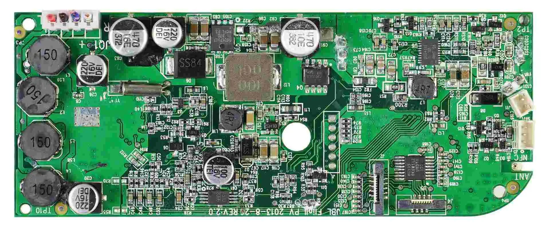
Speeduino PCB is designed to function based on the Arduino Mega platform. This board is specifically designed to offer a low-cost and easy engine management solution for various automotive applications. Speeduino users can make use of the Arduino Mega 2560 boards.
The Speeduino PCB has different versions. Also, this board has hardware requirements which include its output components and input components. Speeduino PCB offers support for about 16bit external analog inputs.
The Inputs of Speeduino PCB
Crack sensor or Camshaft sensor
The crank sensor is crucial for the proper functioning of the Speeduino PCB. Also, the signal that passes through the Arduino has to be within the range of a 0 volt and 5 volt square wave series of pulses. Several opto and Hall sensors must meet the specification of this digital square wave.
The variable reluctance sensors which is also known as VR can be integrated in the Speeduino board. However, since the Speeduino PCB has no signal conditioner required for converting the sine wave to the square wave, there is a need for an additional module.
The v0.3x and v0.4x has the 8-pin DIP socket. Also, the MAX9926 chip has gone through stringent testing to ensure it is compatible with most input signals. It is important to take precautions for electromagnetic interference (EMI) when routing and selecting the wire for the camshaft and crank sensors. Furthermore, it can be helpful when wires are kept away from components that are electrically noisy.
You can as well integrate a shielded cable by fixing the shield to ECU side. Alternatively, you can use software filtering. However, there is nothing as good as having a clean signal from the source. Speeduino PCB users need to ensure that the GND and +12V connections are free of noise if there is a loss in the crank/cam signal.
This sensor has to be one of the 3 wire potentiometer. Your TPS sensor will function well if it is a 3 wire sensor, but you need to be sure it is a potentiometer type sensor. TPS gives account of the present location of the throttle by transmitting an analog voltage signal to Speeduino. Also, TPS is provided with V+ of 5V.
It is advisable to run a test on the TPS when using it with unknown connections. You can use an ohmmeter to test the TPS as this helps in determining the link of each pin. It does this by randomly applying sensor power. You can achieve the following when you disconnect the TPS and the engine is off:
Locate the pair of pins where there is no significant change in the resistance from idle to WOT.
Assign a letter to every pin.
Fix the ohm meter to two pins and run the throttle from idle to wide-open.
The most common TPS sensors feature 3 different pins. If you have a TPS sensor with a different pin numbers, you may have to refer to the engine wiring diagram to reveal the function. This will help you know the types of pins to integrate for Speeduino. You can use a simple code modification for TP sensors working backwards.
Temperature sensors
You can make use of a standard 2-wire thermistor sensor to enable temperature functions. Also, one side of the temperature sensors is linked to a ground.
Manifold pressure
The manifold pressure sensor is integrated in most Speeduino PCB. One of the benefits of this sensor is its support for reading of about 250kPa and it is a good midrange sensor.
Speeduino feature injector drivers which integrate on/off control. These drivers can function well with High-Z injectors. The High Z injectors are also referred to as ‘high-impedance or “saturated since they integrate a full battery voltage to regulate the open cycle of the injector. Generally, the impedance of these injectors is above 8 ohms. The Low Z injectors offer lower impedance. Series resistors need to be installed on these injectors in order to prevent the Speeduino PCB from damage caused by excessive current.
Also, you can use the Ohm’s Law to calculate the watt rating and resistor ohms. Speeduino PCBs are capable of driving about 2 High Z injectors for every output channel. Also, the 0.4v PCB boards feature 2 pins for every injector channel, thereby enabling each injector to connect to the board directly. If there are less than 4 injectors in the application, you can make use of any pin linked to the right channel.
Coils
The most recent versions of Speeduino PCB make use of low-power output signals. These versions are designed to function with external coil drivers. Speeduino can offer great flexibility to regulate the majority of ignition systems. You can directly mount the speeduino outputs to the regular current passive ignition coil.
How does Speeduino PCB regulate ignition circuit power?
The coil driver of Speeduino PCB was mechanical contact points in the past. However, the electronic version replaced these points. The coil driver can be in the Speeduino PCB.
GPIO are multipurpose general programmable input and output modules integrated with the Speeduino standalone. You can program the modules by using the serial port. Also, these modules can work with various processor board types like stm32 and arduino teensy.
Version of GPIO
GPIO mini V0.001
This version offers support to sixteen analog channels, sixteen output channels and sixteen input channels. You can activate the output channels by using logical operations.
GPIO mini V0.002
The GPIO mini V0.002 shares similar features with V0.001. However, the V0.002 can access the values of output channel data from a Speeduino ECU directly connected.
GPIO mini V0.003
This firmware version enables Speeduino to have access to the inputs of the GPIO devices. Also, tis version allows GPIO device to be directly connected to Speeduino through Serial3.
Conclusion
Speeduino PCB has different versions. The most recent versions of Speeduino PCB make use of low-power output signals. These versions are designed to function with external coil drivers. Speeduino can offer great flexibility to regulate the majority of ignition systems.
Are you interested in becoming knowledgeable about iron-based PCBs? Is it your goal to learn how to make iron-based PCBs, what benefits they offer, and where you may put them to use? If that’s the case, you’ve found the ideal site! Deep exploration of iron-based PCBs is our focus. In this article, we’ll deeply dive into iron base PCB, how to make it, what it can do, and how to choose one. Thus, if you want to learn more about iron base PCBs, this is the best article for you!
Iron Base PCB: Definition
An iron-based printed circuit board (PCB) is a circuit board that uses Iron as a substrate material instead of standard FR4 or similar materials. The metal core may be an iron alloy or copper, with copper versions being the most prevalent.
Here are the steps involved in the manufacturing process:
1. Designing the PCB:
The designer creates the circuit’s schematic and converts it into a physical layout optimized for a specific application, size of components, power requirements, and heat dissipation requirements.
2. Choosing the Metal Core:
The metal core consists of aluminum, copper, or Iron. In this case, Iron is the metal core. The thickness is usually between 0.8mm to 3.0mm.
3. Preparing the Metal Core:
Clean the metal core with a degreasing agent to remove dirt or oil from the surface. Next, coat the metal core with a layer of copper using electroless plating, a chemical process that deposits a thin layer of copper using a reducing agent.
4. Applying the Photoresist:
Apply the light-sensitive material (photoresist) to the copper layer using screen printing. The screen lets the photoresist pass through the areas where the designer intends to have the circuit pattern.
5. Exposing the PCB:
UV light passes through a film containing the circuit pattern, exposing the photoresist in the required areas. The areas exposed to UV light harden and become insoluble in the developing solution.
6. Developing the PCB:
Placing the PCB in the developing solution dissolves the areas of the photoresist not exposed to UV light, leaving behind the circuit pattern on the surface of the copper layer.
7. Etching the PCB:
The engineer places the PCB in an etching solution which dissolves the unwanted copper from the surface of the metal core. It then leaves behind a clear circuit pattern on the surface of the metal core.
8. Removing the Photoresist:
The manufacturer then removes the remaining photoresist on the surface of the PCB using a solution that dissolves it. This action makes the circuit pattern visible.
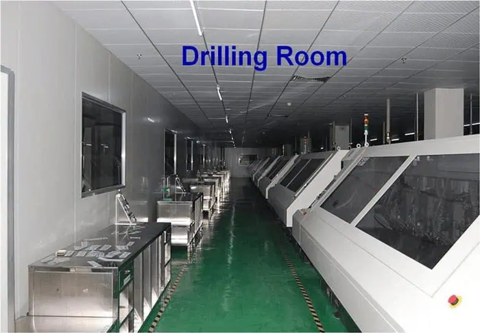
9. Drilling Holes:
Next, the engineer drills holes for components into the PCB using a CNC drilling machine at precise locations and depths.
10. Plating the Holes:
This step involves plating the holes with a thin layer of copper to provide electrical conductivity using electroplating.
11. Applying Solder Mask:
Next, the operator applies a protective layer called the solder mask to the surface of the PCB, using a process similar to screen printing. The solder mask covers the copper traces to prevent oxidation or corrosion and also solders bridges between adjacent components during the soldering process.
12. Applying Surface Finish:
Applying the metal surface finish to the exposed copper traces and pads on the PCB’s surface provides a protective layer that prevents oxidation and ensures the PCB’s long-term functionality. Different surface finishes include electroless nickel immersion gold (ENIG) and hot air.
Iron base PCB has several advantages over typical PCBs. The following are the key benefits of iron base PCBs.
1. Eco-friendly
Iron-based PCBs are recyclable and beneficial to the environment since they comprise Iron and other metals. Therefore, they are more environmentally friendly than non-recyclable PCBs, such as FR-4 or ceramic.
Moreover, iron-based PCBs use less energy than other PCBs to manufacture, which boosts their energy efficiency and reduces their carbonfootprint. These characteristics make iron-based PCBs an environmentally preferable option.
2. Excellent Heat Resistance
Iron base PCBs are particularly resistant to heat. As a result, they can resist high temperatures without losing their electrical characteristics or deteriorating. This feature makes iron-based PCBs appropriate for applications requiring resistance to high temperatures.
For instance, iron-based PCBs are extensively applicable in automobile applications, where engine compartment temperatures can approach 150°C. Additionally, they can survive these high temperatures without problems, guaranteeing that the electrical components continue functioning normally.
3. Good Thermal Conductivity
Iron base PCBs possess excellent thermal conductivity, which refers to the material’s ability to transfer heat from one point to another. Iron base PCBs exhibit much higher thermal conductivity than other PCBs, such as FR-4 or ceramic PCBs. Thus, iron base PCBs are suitable for high heat dissipation applications.
For instance, LED lighting applications commonly use iron base PCBs where efficient heat dissipation from the LED is critical. Additionally, iron base PCBs are applicable in power electronics, where high current flows generate substantial heat. The high thermal conductivity of iron base PCBs aids in dissipating this heat, thereby ensuring that the components operate within their safe temperature range.
4. Magnetic Conductivity
Iron base PCBs are magnetically conductible. Magnetic conductivity refers to a material’s capacity to conduct magnetic fields. Iron base PCBs have a high magnetic field due to the combination of Iron and other metals in their construction. Iron base PCBs are therefore appropriate for uses that call for magnetic conductivity.
In motor control applications, for instance, where magnetic fields are necessary to regulate the rotation of the motor, iron base PCBs are frequently applicable. Furthermore, Iron base PCBs can offer the required magnetic conductivity for effective motor operation.
5. High Insulation Performance
Iron base PCBs have excellent insulation performance. Insulation performance refers to the ability of a material to prevent the flow of electricity through it. Iron base PCBs combine Iron and other metals, which makes them highly resistant to electrical current. This feature makes iron base PCBs suitable for applications that require high insulation performance.
For instance, iron base PCBs commonly apply to power electronics with high voltage and current levels. Iron base PCBs can provide the necessary insulation to prevent any electrical leakage or shorts, thus ensuring the safety and reliability of the electronic system.
When it comes to selecting the right iron base PCB for your application, the following are the factors that you should consider:
1. Copper Thickness and Trace Width:
The amount of current that can flow through the traces on your PCB significantly depends on the thickness of the copper within it. Higher current flow is possible with thicker copper, which is crucial for power electronics applications. However, the width of the traces is equally essential to thickness. Narrower traces offer more resistance, which can cause overheating and reduced performance. As a result, it’s crucial to ensure that the copper thickness and trace width are ideal for the application in question.
2. Power Dissipation and Heat Generation:
It would be best to consider your circuit components’ power dissipation and heat generation when choosing an iron base PCB. Power electronics components produce a lot of heat, so picking a PCB that can efficiently disperse this heat is crucial. Iron base PCBs are famous for their exceptional thermal conductivity, but it’s essential to ensure that the thermal design of the PCB is ideal for your specific application. Checking your component placement, heat sink application, and PCB layout to ensure airflow are all examples of this procedure.
3. Dielectric Loss and Thermal Expansion:
The dielectric loss and thermal expansion of your PCB substrate may also impact your circuit’s performance. Dielectric loss is the quantity of energy lost when we subject a substrate to an electrical field. A higher dielectric loss may result in a rise in heat production and a decrease in performance. Similarly, thermal expansion describes how much the substrate expands or contracts due to temperature variations. Over time, this may cause the components to experience stress and lose reliability. Therefore, it is crucial to use a PCB substrate with low dielectric loss and regulated thermal expansion to achieve optimum performance and dependability.
The following are the industries that frequently use iron-based PCBs:
1. Automotive: Iron-based PCBs are applicable in vehicles’ fuel injection controllers, airbag systems, and engine control units. Iron-based PCBs are sturdy, long-lasting, and temperature-resistant, which makes them perfect for automotive applications.
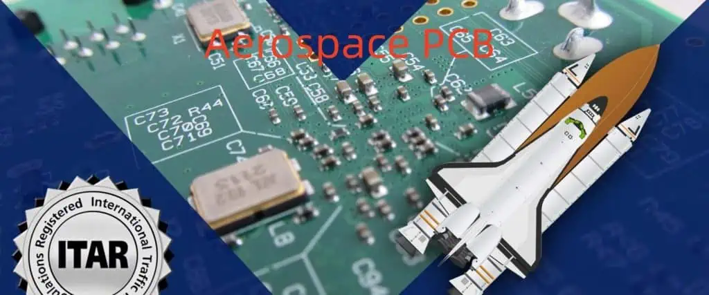
2. Aerospace: Iron-based PCBs also apply to avionics, navigation, and flight control systems, among other aerospace applications. Iron-based PCBs are perfect for aircraft applications because they are lightweight and have great electrical and thermal qualities.
3. Medical: Iron-based PCBs suit various electro-medical devices, patient monitoring systems, and medical imaging applications. Because iron-based PCBs are radiation and corrosion-resistant, they are perfect for medical applications.
4. Industrial: Industrial settings like robots, control systems, and factory automation apply Iron base PCBs. These PCBs are excellent for industrial applications because of their outstanding dependability and longevity.
5. Consumer Electronics: Products including mobile phones, tablets, laptops, and LED Televisions employ iron-based PCBs. Iron-based PCBs are perfect for consumer electronics because they have good electrical characteristics and are corrosion-resistant.
Conclusion
In conclusion, from the above details, iron-based PCBs are an excellent choice for applications requiring robustness and heat resistance. These eco-friendly PCBs have high thermal conductivity and can withstand high temperatures. They are applicable in automotive, aerospace, and industrial electronic applications. When selecting an iron-based PCB for your application, you must consider the copper thickness and trace width, power dissipation, heat generation, dielectric loss, and thermal expansion. Thus, if you’re in the market for an iron base PCB, remember these considerations, and you’ll strike while the Iron is hot!
It is crucial to stay current with the newest technology and techniques as the printed circuit board manufacturing industry advances quickly. Modern PCB manufacturing is a significant industry in Israel, where a number of top businesses provide high-quality, reasonably priced printed circuit board design and production services. These companies, ranging from EDAIS Integrity Solutions Ltd to Trace PCB, are experts in creating surface mount and through-hole assemblies and single-sided, double-sided, and multilayer printed circuit boards. Moreover, customers get efficient and cost-effective circuit board solutions with the assistance of these firms.
However, these firms also come in vast numbers, which makes it pretty challenging to select the right one without proper guidance. So how can you select the right printed circuit board manufacturing company in Israel? Which factors should you consider when selecting the printed circuit board manufacturing company? And why should you choose to work with these manufacturing companies?
Israeli PCB manufacturing company Trace PCB was established in 1988. The business specializes in producing rigid and flexible circuit boards, surface mount and through-hole assemblies, and single, double, and multilayer PCBs. Trace PCB is a quality-focused business that offers quick turnaround on high-quality PCBs. The company has been UL-approved since 1999 and is ISO 9001:2015 and ISO 14001:2015 certified. Trace is capable of designing, developing, and producing custom PCBs for several applications thanks to its workforce of skilled engineers and technicians. In addition, trace can provide customers with effective and affordable solutions for their PCB needs by offering services like PCB layout and assembly.
Advanced Printed Circuit Board Production Solutions
Trace Printed Circuit Boards follow emerging trends in the circuit board industry, which helps them generate more innovative printed circuit boards. Moreover, this trend also allows them to create more sustainable solutions in the modern era.
A great high point of this trend is that Trace can now effectively follow and apply the latest printed circuit board technologies. And by utilizing the latest technology and its impeccable personnel, this company can implement the requirements and capabilities in modern PCB designs.
Israeli PCB manufacturer Print Electronics was established in 1982. Print Electronics is an industry leader in producing rigid and flexible circuit boards, single, double, and multilayer PCBs, as well as other associated services. The company has been UL-approved since 1999 and is ISO 9001:2015 and ISO 14001:2015 certified. Customers can choose from a wide range of services provided by Print Electronics, including PCB design, layout, manufacturing, and assembly. Additionally, the business may offer customers turnkey assembly and rapid turnaround times as PCB solutions.
Reasons why you should work with Print Electronics
Print electronics is a great company that has an impressive reputation. Here are a couple of reasons why you should choose to work with this company:
Highest Flex Printed Circuit Board Production Standards
When selecting a PCB manufacturer to handle the assembly of your flexible printed circuit board, you should highly consider the standard and the quality of the circuit board.
Print electronics does an impressive job on this part since it offers impeccable manufacturing standards for flex printed circuit boards.
These impeccable manufacturing standards are put in place since the manufacturer has invested heavily in the utilization of advanced gadgets that helps them produce high PCBs with high precision.
Moreover, these gadgets are also utilized to offer support to the PCB production process of any type of circuit board ranging from flex to rigid-flex printed circuit boards.
Mass Production
The Print Electronics Company also aims to produce and design flex PCBs within less than 24 hrs. However, this case is only applicable to low-volume manufacturing processes.
On the other hand, if a client needs their PCB produced in bulk, this company contacts its overseas business partners, and they tackle the task together. The utilization of outsourced workforce helps them generate printed circuit boards in less time compared to most PCB manufacturers.
Multiple PCB Production Processes
Print Electronics covers a vast range of PCB productions. These productions include:
A PCB manufacturer with its headquarters in Israel, Newline PCB focuses on creating high-quality, economical PCBs. With an emphasis on quick-turn PCBs, the company offers a variety of PCBs and components. A team of highly skilled and qualified employees at Newline PCB are able to provide professional guidance and support throughout the complete PCB process.
Single-sided, double-sided, and multilayer printed circuit boards are the area that Newline PCB majors in primarily. Moreover, the firm offers a complete array of PCBA services, such as surface mount and thru-hole Tech assembly. Additionally, a comprehensive range of services are provided by Newline PCB, including PCB design, layout, prototype, and manufacturing.
Flex PCB Solutions
Here are some of the most common services or solutions that this company provides to its flex PCB clients:
Component sourcing
The Newline-PCB Manufacturing Company has a pretty extensive list of printed circuit board suppliers in the East and Israel. Therefore, this company doesn’t have a challenging time placing orders or sourcing components for the production of printed circuit boards.
PCB Testing
Newline is a great company that focuses on client satisfaction and implements various tactics to keep its clients happy.
One tactic that this company utilizes is effectively checking on the flex PCBs and other types of PCBs after production, both electronically and visually, before shipping. Doing so helps them catch errors before they ship the order to the client.
Multiple PCB Productions
Newline provides a lot of options when it comes to the manufacturing process of flex PCBs. Moreover, with these impeccable manufacturing capabilities, clients can choose to use mass and low-volume PCB production levels for their circuit board projects.
Kaizen Technologies
Leading PCB manufacturer Kaizen Technologies is situated in Israel and specializes in manufacturing PCBs that have impeccable quality and that are economical. The firm has an great workforce which has impeccable experience and understanding that they utilize to offer professional guidance and help during the complete Printed circuit board manufacturing process. The fabrication of single-sided, double-sided, and multilayer PCBs is a specialty of this company.
The firm also offers a complete array of PCBA services, for example, SMT and thru-hole assembly. Moreover, Kaizen Technologies provides a vast array of services, for example, PCB design, layout, prototyping, and manufacturing. The business offers the best customer service, with a helpful, knowledgeable, and experienced crew on hand to address clients’ questions or concerns.
Kaizen offers multiple services to its clients. However, this isn’t the only reason you should choose to work with this reputable company to make your PCB project successful. Here are more reasons why you should select Kaizen to handle your PCB Order in Israel:
Unique Management
The Kaizen Tech Management is fully committed to effectively satisfying the company’s clients. That is why this management places a premium division in the company that handles customer support.
Improved Production Reliability
Generally, KaiZen Tech utilizes high-quality PCB components to manufacture PCBs. The utilization of these components ensures that they produce high-quality PCBs each time. Moreover, this company also has strong relations with some great PCB component suppliers that they use to source durable and high-quality components for their PCBs.
Short Timetable
Kaizen tech typically wants you as their client to get back your order fast. To achieve this, KaiZen utilizes a short lead time to effectively design your PCB without affecting the quality and durability of the PCB.
Israel Taiwan
Israel Taiwan Production Center (ITPC) was founded in 2008 as an Israeli PCB fabrication and assembly service provider. It is headquartered in the Tel Aviv region, and its current CEO is Shmuel Yitzhak. The firm provides a vast array of services, such as high-frequency PCBs, HDI, and jet printing. In addition, the company can manufacture rigid and flexible PCBs and high-speed Boards using pulse width modulation (PWM). ITPC additionally offers PCB assembly services, such as surface mount technology (SMT), through-hole technology (THT), and chip-on-board (COB). The organization has ISO9001, ISO13485, and UL certifications, and its services adhere to J-STD-001, IPC-A-610, and IPC-A-620.
Israel Taiwan Production Center has become one of the primary Israeli PCB manufacturing and assembly services producers. Moreover, this company can generate both rigid and flex circuit boards since it specializes in high-frequency PCBs, HDI, and jet printing. In addition, ITPC has ISO9001, ISO13485, and UL certifications, and its services adhere to J-STD-001, IPC-A-610, and IPC-A-620. So, the organization is qualified to manage even the most intricate PCB projects.
Main Products
Israel Taiwan Generally handles the following electronic services and products:
The company handles all these processes and products with excellent efficiency and precision. Therefore, if your project falls under this category, this company will help you.
Founded in 2014, the Israeli company Flexitech Avia Printed Electronics offers PCB fabrication and assembly services. It is based in the Tel Aviv region, and Ami Bar-Lev currently serves as the CEO. High-frequency PCBs, HDI, and jet printing are just a few of the many services provided by Flexitech Avia Printed Electronics. The business can also create stiff and flexible PCBs and high-speed Boards with pulse width modulation (PWM). Moreover, Flexitech Avia Printed Electronics offers PCB assembly services using chip-on-board, through-hole technology, and surface mount technology (SMT) (COB). The business has UL, ISO9001, and ISO13485 certifications, and its services adhere to J-STD-001, IPC-A-610, and IPC-A-620 standards.
One of Israel’s top companies offering PCB fabrication and assembly services is Flexitech Avia Printed Electronics. The business produces both rigid and flexible PCBs and specializes in high-frequency PCBs, HDI, and jet printing. Moreover, Flexitech Avia Printed Electronics has UL, ISO9001, and ISO13485 certifications. Additionally, its services adhere to J-STD-001, IPC-A-610, and IPC-A-620 requirements. As a result, the business is prepared to manage even the trickiest PCB projects.
MILPCB
Established in 2011, MILPCB is an Israeli-based circuit board fabrication and assembly services provider. Itzik Shmueli, the CEO, is currently in charge of the business, which is based in the Tel Aviv region. Among the many services provided by MILPCB are high-frequency printed circuit boards, HDI, and jet printing. The business can also create stiff and flexible PCBs, as well as high-speed Boards with pulse width modulation (PWM). Moreover, MILPCB offers PCB assembly services using chip-on-board, through-hole technology, and surface mount technology (SMT) (COB). The business has UL, ISO9001, and ISO13485 certifications, and its services adhere to J-STD-001, IPC-A-610, and IPC-A-620 standards.
One of the top companies in Israel offering PCB fabrication and assembly services is MILPCB. The firm manufactures both rigid and flex-printed circuit boards and specializes in high-frequency PCBs, HDI, and jet printing. Moreover, MILPCB has UL, ISO9001, and ISO13485 certifications, and its services adhere to J-STD-001, IPC-A-610, and IPC-A-620 requirements. As a result, the company is prepared to effectively manage even the trickiest circuit board projects.
Leading Israeli companies that offer PCB design and manufacturing services include EDAIS Integrity Solutions Ltd. The business is headquartered in Petah Tikva, Israel, and was established in 2006. EDAIS produces high-end PCBs specifically for cutting-edge industries like aerospace, automotive, medicine, and military. Along with making custom PCBs, EDAIS also offers complete turnkey PCB prototyping, assembly, and testing solutions. The highest standard of quality and customer service are priorities for EDAIS while serving its clients.
Conclusion
The emergence of Israel as a significant player in the global printed circuit board market is apparent. From the UL-approved Trace Printed Circuit Board to the comprehensive services of EDAIS, the country is home to some of the most reliable and innovative Circuit Board manufacturers around. Whether you’re looking for a high-end, top-tier PCB or something more economical, these Israeli companies have the ability and expertise to deliver. With the proper PCB manufacturer, you can rest assured that your project will be in safe hands.
The electrical and electronics industry in Vietnam contributes a lot to their economy. This industry has made Vietnam one of the most significant exporters in the world as of the 21st century. Moreover, printed circuit board production has so much potential to expand this country’s market size since it is a core component of almost all electronics products.
In realizing the benefits of investing in the printed circuit board industry, many foreign companies are now investing in the Vietnamese PCB manufacturing industry. Moreover, Vietnamese companies are also generating printed circuit board manufacturing firms nationwide. So as of now, there are numerous PCB manufacturing companies. But out of the many PCB manufacturing companies that exist in Vietnam, which ones are the best? And which ones should you consider working with to make your PCB project successful?
Before we move on to discuss the best PCB manufacturer in Vietnam, let us first look at the definition of a printed circuit board:
Generally, a printed circuit board or a PCB is a thin sheet of insulating components, for example, fiberglass. The insulating parts usually have metallic tracks or circuits etched or printed onto them for efficient electrical conductivity. Most, if not all, modern electronics come with printed circuit boards ranging from mobile phones to tablets, keyboards, laptops, computers, and so much more.
PCB Materials
Typically, different types of PCBs come with varying base materials. The materials the manufacturer chooses to utilize as the base component of a PCB depending on the application area of the PCB. Moreover, the base material must meet several conditions, which include the following:
It should be heat resistant
It should be durable
And lastly, it should be insulating
Some of the most common materials manufacturers utilize to make PCBs include:
Printed circuit boards come in many different variations, which include the following:
Rigid-flex PCBs
Flexible PCBs
Rigid PCBs
Multilayer PCBs
Double-sided PCBs
Single sided PCBs
The Best PCB Manufacturer in Vietnam
Vietnam has a lot of Printed circuit board manufacturers. Here are the top PCB manufacturers in this country that guarantees high-quality PCBs each time:
Fab 9
Fab 9 is a PCB manufacturing company in Vietnam that hit the market back in 2007. The company’s headquarter is in Binh Duong Province, Dong An Industrial Park in Vietnam.
Fab 9 offers a “one-stop solution” by catering to all your PCB production needs. Moreover, this company has over fifteen years of experience dealing with PCB production in Silicon Valley and Vietnam.
The goal of Fab 9 is to offer impeccable services and resources to their customers and to generate, launch and sell durable and high-quality printed circuit boards and PCB products.
Cicor is a PCB manufacturing business that focuses on creating a range of printed circuit boards (PCBs). In addition, the company provides various services, including PCB design, manufacture, assembly, and testing. Medical, automotive, computer, communications, and industrial electronics applications are just a few of the ones that Cicor’s products are employed heavily.
The key benefit of Cicor is its capacity to provide a broad range of services to its clients. That comprises PCB design, fabrication, assembly, and testing to guarantee that clients receive the best products that satisfy their needs. Also, Cicor has a strong customer care group that is committed to assisting clients with any problems or inquiries they may have.
The modern production and assembly facilities at Cicor are another benefit. These facilities are furnished with cutting-edge machinery and technologies, enabling the company to create PCBs of excellent quality and dependability. Cicor also employs the most up-to-date manufacturing techniques to guarantee the best possible quality for its products.
The price of Cicor is the sole drawback. Compared to other PCB production companies, the company’s products are rather pricey. Yet, buyers can rest easy knowing their money will be safe because the company’s products are of a high caliber and worth the price.
Generally, Cicor is a reputable PCB manufacturing business that provides a vast array of services and high-quality goods. Customers receive the highest-quality goods tailored to their demands thanks to the company’s cutting-edge production and assembly facilities and skilled customer service staff. Although some of its items can be pricey, their high caliber and dependability make them worthwhile purchases.
Main Products and Business
Typically, Cicor handles the following processes and products:
Fujitsu is a Vietnam-based PCB manufacturing company that hit the market back in 1999. The company’s headquarters is at Me Tri Ward in Tu Liem District, Vietnam.
The company has a long history of generating impeccable experiences and ideas. Moreover, Fujitsu strives to advance its clients and society as a whole. Furthermore, this company drives the success of its clients and promotes a more efficient and sustainable world by combining cutting-edge tech and impeccable integration capabilities.
Fujitsu tries its best to bring cross-industry and high-tech functions to your business focus. Moreover, this company is committed to altering the whole world and making it a place where we can exist in impeccable prosperity via Fujitsu Uvance.
Main Products
Generally, Fujitsu deals in the following products and processes:
Vietnam-based Jong Gong is a printed circuit board manufacturing business. The business specializes in creating high-quality printed circuit boards (PCBs) for use in various electronics, including consumer electronics, medical devices, and communication systems. Jong Gong offers boards for both mass manufacturing and prototypes. In addition, the company provides a wide range of services, including designing PCB layouts, placing components, and assembling and testing products.
Jong Gong is renowned for its quick lead times and high-quality goods. The business employs cutting-edge technology to create printed circuit boards with precise tolerances. They also use cutting-edge testing methods to ensure the boards satisfy the necessary quality standards. The company produces both single-sided and multilayer boards. Clients can select from several materials, including laminates made of polyimide, FR-4, and copper-clad laminates.
Working with Jong Gong has certain benefits, one of which is their affordable cost. Additionally, the business provides a vast array of customized services to fit consumers’ requirements. Also, the firm provides numerous payment methods and offers discounts for large orders.
If you decide to work with Jong Gong however, you might face a few drawbacks, the biggest one being occasionally sluggish customer-company communication. As the organization is headquartered in Vietnam, it could be challenging to contact the client immediately. Also, as the company does not warrant its goods, clients should always be alert for potential PCB problems.
Overall, Jong Gong is a reputable PCB manufacturing company providing affordable premium goods. However, customers should always be aware of potential communication problems while dealing with the business.
Main Products
Generally, Jong Gong specializes in the following areas:
Meiko is a Vietnam-based printed circuit board manufacturing company established in 2007. The company’s headquarters is in Cam Giang District in Hai Duong, Vietnam.
Generally, this company provides cutting-edge PCB production, for example:
Any Layer HDI – this PCB production allows free connection between various PCB layers. Moreover, this product helps generate PCBs that fit in handheld gadgets such as mobile phones and tablets.
Moreover, this company provides high heat dissipation and high current printed circuit boards that are durable and resistant to various harsh environments, for example, the interior parts of a solar power generator or automobile engine.
Meritronics hit the market in 1995; since then, it has been a force to reckon. The company is located in Nam Tu Liem District in Hanoi, Vietnam.
Meritronics offers complete electronic PCB design services which help their clients bring their products to the electronics market fast and efficiently. Moreover, this company has impeccable experience, which gives their clients peace of mind in terms of quality production.
The company major in providing the following services:
Moreover, this company also offers functional test processes, cost reduction designs, product reliability tests, concept, and industrial design rendering, circuit testing, process design, and operational test procedures. Additionally, meritronics also processes clients’ designs to ensure they meet their expectations.
Main Products
Generally, Meritronics deals in the following processes and products:
Mold design
3D modeling
Mechanical design
Printed circuit boards design
Firmware and hardware design
SAOKIM
Saokim is a Vietnam-based company that has been around since 2004. The company’s headquarter is in Ho Chi Minh City in, Vietnam. Since the company has been around for some time, it has impeccable experience in terms of handling printed circuit boards and electronics in general.
Typically, this company handles SMT Glued component processing, electronics assembly, and electronic PCB assembly. Moreover, Saokim also majors in PCBA and bulk printed circuit board production, which makes them the perfect choice if your project requires PCBs in bulk.
To generate high-quality and precision printed circuit boards, Saokim utilizes high-quality gadgets and high-tech testing equipment that ensure accuracy each time. Additionally, this company complies with the ISO-9001 2008 standards when producing printed circuit boards which help them maintain their quality PCB production process.
Main Products
Saokim deals in the following processes and products:
Circuit board assembly
Bulk-printed circuit board production
Multilayer printed circuit boards
Single-layer printed circuit boards
Sunching
Sunching was established back in 2001 and its headquarter is based in Binh Duong Pro in Vietnam. The company utilizes cutting-edge technology to cater to a pretty wide range of PCB requirements for its clients worldwide. Moreover, the company utilizes most of its resources to offer impeccably high-quality PCB products, guaranteed lead times, and impeccable after-sale services to its clients.
The environmental management program and manufacturing firms of this company are all ISO 14001 and ISO 9001 certified. Moreover, all products that ship from this company meet international UL safety standards.
Sunching is pretty confident in terms of always delivering high-quality products to its clients. However, to achieve this, the firm has to utilize impeccable R&D skills, high-tech gadgets, and extensive experience in the industry. But overall, this is a company that you should try out if you are looking for quality services and products.
Main Products
Generally, Sunching handles the following products and processes:
Vector or Vector Fabricator is a Vietnam-based PCB manufacturing company that has been in the PCB industry since 1995. The company’s headquarter is in An Town, Binh Duong in, Vietnam.
The establishment of Vector was to help support electronics engineers and the generation of more efficient electronic products. The company knows that PCBs have multiple applications in various industries, which includes the medical and military sectors. Moreover, the company also keeps in mind the fact that the complexity of various PCBs tends to vary according to the application area of the circuit board. Therefore, to cater to various PCB requirements, Vector utilizes cutting-edge tech and highly trained employees. Moreover, this company also constantly trains its employees; consequently, they are always in the know in terms of innovative production processes or changes in the manufacturing process.
Main Products
Generally, this company handles the following products and processes:
Vexos is another famous PCB manufacturing company that is based in Vietnam. Although the company hit the market back in 2019, it has been growing pretty fast. The headquarters of this company is in Ho Chi Minh City in, Vietnam.
Vexos offers mid-to-low volume, high complexity, high mix, and complete service electronics manufacturing. Moreover, this company also provides custom material solutions. Therefore if your PCBs need extra customization, this company might help you.
Vexos is committed to providing high-quality products. Actually, this commitment has seen Vexos work with various groups of manufacturers that generate original electronic gadgets.
Main Products
Generally, Vexos handles the following processes and products:
Unigen is among the oldest Vietnam-based PCB manufacturing companies since it was established in 1991. The company’s headquarters are in Tu Son Township, Bac Ninh Province, in Vietnam.
Since Unigen hit the market, it has grown to become a global leader in the production and design of bespoke and original solutions for flash and DRAM storage. Moreover, this company has multiple manufacturing firms spread out across the world, which include:
A manufacturing firm in Silicon Valley which is IO 13485/14001/9001 certified
A manufacturing firm in Hanoi that is ISO 14001/9001 certified
Moreover, this company sells its electronics products to multiple OEMs worldwide in the medical, automotive, imaging, telecommunication, server, industrial, and embedded devices industries. Additionally, Unigen offers impeccable EMS (electronics manufacturing services), for example:
Intro of volume and new products
Supply chain management
Post-sales support
Testing
Assembly
Main Products
Unigen mainly handles the following processes and products:
Trung Nam EMS is among the more recent Vietnam-based printed circuit board manufacturing companies that hit the market in 2020. The Trung Nam EMS Vietnam base is located in Hoa Vang District, Danang City.
Although Trung Nam EMS hasn’t been around for a while, it has become pretty popular due to its utilization of high-tech gadgets to gain impeccable precision. Moreover, this company also offers various manufacturers worldwide impeccable assembly designs and electronic components.
Main Products
Trung Nam EMS mainly offers the following product and processes:
Rigid-flex and flex PCB designs
Burn-in and tests
Electronics prototypes
Box build/system
Logistics and supply chain
Printed circuit board assembly
PCB engineering and design
Conclusion
Printed circuit boards are, without a doubt, crucial components in most, if not all, electronic gadgets. However, these components also need complex processes to generate. Luckily there are multiple manufacturers spread out across the world that offer PCB production services. Unfortunately, however, not all PCB manufacturers provide high-quality services and products. Therefore we hope this article will help you find the right match if you are looking for a PCB manufacturer in Vietnam.
Being aware of the variety of Circuit boards is crucial for engineers. An essential component of the Circuit board industry is populated PCB. A PCB would just be a naked board without it. Professionals handle this part to prevent any errors.
The populated PCB affects a circuit board’s operation and performance. It is essential to comprehend what the PCB populace consists of. We will go over significant information about the populated PCB in this essay.
What Does a Populated PCB Mean?
Any circuit board having electronic components is called populated PCB. are boards are one that doesn’t have any installed electronic components on it. A PCB may therefore be either populated or bare. PCBs could be filled using through hole or the surface mount method.
A PCB assembly is identical to a populated pcb. These board’s components are surface-mount devices. Electrical equipment which links electronic components is known as Populated PCB. This PCB has conductive tracks, pads, and other features.
To create the populated PCB, manufacturers help in soldering electronic components onto the board. IC, diodes, and capacitors are some of the components on the populated PCB. The bare board lacks electronic components, but populated PCB does.
It’s critical to recognize the distinction between the populated PCB as well as PCB fabrication. The creation of the bare board is a step in the PCB manufacturing process. A circuit board prototype is made throughout the production process. The way a PCB is filled is dependent on a circuit board’s intended use.
An aspect which involves some processes includes PCB population. While populating the board, the planning, the organizing as well as sorting are highly crucial.
Sanitize the bare PCB
The process of filling the circuit board starts with this. So clean the board to get a populated PCB that works. You should clean the PCB prior to and following filling it. You can successfully execute soldering by cleaning your Board.
Fill PCBs starting at the lowest level and working your way up
If you’re not careful, PCBs could get overpopulated. Your situation is made more challenging by the overpopulated PCB. It gives you very little room to mount your components where they need to be. Planning ahead is the preferred approach to stop overpopulation from happening. Connect your components using solder throughout the bare boards.
Start by placing the cheapest component on the board. By doing this, large objects won’t get in the way.
Use tweezers
Tweezers are required for through-hole mounting. You can put the thru-hole components on top of your circuit board with the aid of tweezers.
Use a tool for component leads.
The tool for component leads bends lead components of all sizes and shapes while measuring hole spacing. Use this tool for maintaining the stability of your circuits. It can be useful to bend the component leads onto the proper lead width.
Use poster putty to create helpful hands.
Among the populated PCB, poster putty serves as a underutilized tool. While working on little objects, this tool could assist in holding them. In place of traditional extra hands tools, poster putty may be utilized. This tool will not leave behind any traces on the PCB whenever it is used.
Insulation made using hot glue
Hot glue could serve as a barrier when attaching components on Boards. Hot glue shouldn’t be used to components that are thermally sensitive, though. You can secure cables in the proper location with hot glue.
Plan your enclosure
In the process of populating the PCB board, this is crucial. A circuit board’s size and shape are constrained by enclosures. Choose an enclosure which satisfies the demands of the planned use.
Do not handle or reposition as much
Circuit boards need to be moved around more often, which extends the time needed for the population of the PCB. When the board becomes two-sided and there are components present on both sides of a PCB, repositioning is necessary. Using all the components of the SMT on one side of your board is advised.
Manufacturers employ two main methods for creating the populated PCB. These methods include through-hole and surface-mount. A PCB can be populated using THT and SMT.
SMT
This can be described as a typical method of populated PCB. Manufacturers mount delicate components using SMT. The components in the SMT have short leads. Moreover, this method populates components on the circuit boards using automated machinery. Direct SMD mounting on the Circuit board is known as SMT. Manufacturers utilize pick & place machines to populate the circuit board.
THT
The pins for the components are inserted into the board’s holes using the thru-hole method. Here, the component placement must follow the guidelines of the through hole process. This method is used by manufacturers to position a component onto circuit boards.
Manufacturers, however, insert components containing leads through plated thru holes in THT. Before the invention of SMT, this method of filling boards was widely used.
Factors Affecting the Populated PCB
While populating the bare board, manufacturers need take a few things into consideration. Several elements have a direct impact on the populated PCB process.
Portion size
The size of the electronic parts on circuit boards varies. The size of the components must be taken into account by the manufacturer when choosing the process speed. The device for pick and place will adjust for part size.
Speed of placement
The process of populating the PCB entails attaching components to bare circuit boards. There are many processes involved in this aspect.
Reducing the amount of processes will speed up placement for manufacturers. For instance, if components are pointing in the same direction, you can position them without rotating them.
Board types
PCBs come in a variety of forms. How and where to populate it will depend on the type of board. Multilayer board types will have a different population than the single layer boards.
A filled PCB comes with many benefits. It is crucial to understand that populated PCBs are what are employed in the production of electronics. In the absence of electronic components, the bare PCB is inoperable. In our electronics world today, populated PCBs are crucial.
Compact design
Putting electronic parts on the circuit board results in a small and compact design. Thus a Circuit board designer can try to create a fantastic design when filling a PCB. Connecting the components coupled with enabling input and output connections are populated PCBs.
Great option
For many businesses, a populated PCB is a dependable choice. It is a dependable alternative that may be used in a variety of products. These boards are durable. Manufacturers fill a board according to a predetermined pattern. This enhances the consistency of these boards.
Inaudible electrical noise
In circuits, electronic noise could easily happen. The components are mounted by the manufacturer to minimize the electronic noise generated by this circuit. Path lengths can be shortened by populated PCBs to cut down on electromagnetic emission.
Repair is simple
Every board flaw can easily be tested for and found. As a result, producers can quickly spot a defective component then replace it. This can be done without affecting other electronic parts of the circuit board.
In military equipment, populated PCB is frequently employed. The increased demands of our military industry are being met by these boards. In military equipment like the machines for missile detection, populated PCBs are found. Nonetheless, producers create populated PCBs of high frequency ffor use in the military.
Electronics like TVs and remote controls work with the populated PCB. The core of such devices are these types of circuit boards. They provide these devices with mechanical as well as electrical support. Connected boards that have been populated aidS in the creation of laptops and Cellphones.
Medical industry
There is yet another use for populated boards. There are more and more populated PCBs being used in the medical sector. These circuit boards are excellent for tracking diagnosis, therapy, and other procedures. These boards can also be found in ultrasound, CAT, as well as other medical equipment.
Aerospace
Populated PCBs are also used in the aircraft sector. Inside this application, high-speed as well as high-frequency boards are used. They seem to be more susceptible to challenging circumstances, which explains why. This PCB is used in aerospace technologies like satellites, aircrafts, and radio communication system.
Populated PCBs work well in a variety of applications. They are excellent in every way, making them suited for the majority of applications.
Conclusion
The electronics industry places a high value on populated PCB. This board has several uses and is widely employed. The majority of electrical devices rely on them as their core. The populated PCB is produced in large part by the PCB population. This procedure needs to be followed attentively. Technology advancements have made PCB population simpler.
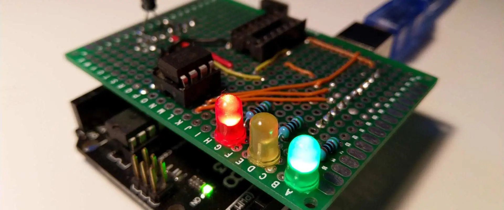
There are several open-source platforms for developing electronics projects. Arduino is one of such platforms. It is specially designed for creating and developing several electronics projects. Comprising a physical programmable circuit, and Integrated Development Environment, the Arduino can be used in uploading and writing computer code to a physical board. The physical programmable circuit board of Arduino is known as the microcontroller while the integrated development environment is the software.
Over time, the Arduino board has gained popularity among people who just started developing electronics. This is because Arduino is different from other programmable circuit boards developed in the past. Unlike those boards, Arduino requires no programmer to load a new code. All you just need is a USB cable and you are good to go. Asides this, Arduino offers several features and benefits.
Arduino features various boards. The Arduino UNO PCB belongs to the Arduino family. To explore the Arduino UNO PCB, you need to understand how it functions, its features and how to integrate it in your electronic project.
The Arduino UNO PCB comprises a physical programmable circuit and a piece of software. As a microcontroller, this board integrates the ATmega328. The Arduino board is a popular board which belongs to the Arduino family. It is a user-friendly board for beginners as it helps them build their electronic projects with much ease. Due to the features of this board, it is the most popular of all the Arduino boards.
Arduino UNO PCB comes with a lot of components which include 14 digital input/output pins, a USB connector, ICSP header, a power jack, and a reset button among others. These components are crucial in ensuring the functioning of the Arduino UNO PCB. Also, a USB port is used in charging this board. However, you can charge the Arduino board with its DC supply.
Components of the Arduino UNO PCB
As earlier mentioned, Arduino UNO PCB features various components which play crucial roles in its functioning. Arduino boards are available in various types. However, these components are common in Arduino boards.
USB Port
All Arduino boards feature a USB. There is a need to connect these boards to a power source. Therefore, the USB cable from a computer can power the Arduino UNO PCB. Also, this board can be powered by a power supply in a barrel jack. Arduino UNO PCB comes with a barrel jack and a USB connection cable. Another function of the USB connection is that it enables users to load code on the board.
Reset button
The Arduino UNO PCB features a reset button. If you intend to connect the reset pin to ground, you just need to push the button and then restart code loaded on the board.
Main IC
The main integrated circuit of the Arduino UNO board looks like metal legs. This component is the brain of the Arduino UNO board. In Arduino boards, the main IC differs. The main IC of the Arduino UNO PCB is different from another Arduino board. However, the main IC of the Arduino boards always comes from the ATmega line.
It is important to know the type of IC before you load a new program. The details of the main IC are usually written on the IC’s top side.
The Arduino UNO PCB features a LED which lights up anytime the board is plugged to a power source. The LED is just beneath the word “UNO” on your UNO PCB. If the LED on the Arduino UNO board fails to come on, something might be wrong. This can help you easily detect any problem with your board.
Voltage regulator
Another important component on the Arduino UNO PCB is the voltage regulator. This component regulates the amount of voltage that passes into the board. It is like a gatekeeper that rejects any extra voltage to your board. This extra voltage might be harmful to your circuit board. The Arduino UNO PCB has its voltage limit. Avoid connecting this board to a device with more than 20 volts.
TX RX LEDs
RX simply means receive while TX means transmit. The TX RX markings indicate the pins for serial communication. In the Arduino UNO PCB, you can see the TX and RX in two places. You will see it next to the TX and RX indicator LEDs. With these LEDs, users can know when the board is transmitting or receiving data. Therefore, the TX RX LEDs is a good indicator.
Pins
Every Arduino board comes with pins. However, the number of pins may differ according to the types of board. The pins provide space for connecting wires to develop a circuit. These pins feature plastic headers that enable users to plug a wire right in the board. There are different types of pins on the Arduino UNO PCB. Each of these pins is labeled. These pins serve various functions.
Crystal Oscillator or Ceramic Resonator
A microcontroller like the Arduino board requires a clock source. The operation of the microcontroller depends on the clock circuit. Also, the clock frequency determines the instructions per second a microcontroller will carry out. The ATmega series is usually integrated in Arduino boards. These microcontrollers can integrate two different clock sources.
The Arduino UNO PCB has various types of pins. Each of these pins has its own functions. Also, it is crucial in the functioning of the Arduino board. Here, we’ll be discussing the various pin types on the Arduino UNO PCB.
Arduino UNO PCB comes with six analog pins. These pins are labeled A0 to A5 on the board. Analog pins are capable of reading the signal coming from an analog sensor. For instance, they can read temperature and convert to a digital value.
AREF
AREF refers to Analog Reference. The AREF pin is usually integrated in setting an external reference voltage.
GND
GND is the short form of ground. The Arduino UNO PCB comes with several ground pins. Users can integrate any of these pins to ground their circuit.
Digital
The Arduino UNO board comes with several digital pins. These pins can tell if a button has been pushed. They are ideal for both digital output and digital input.
5V and 3.3V
The 5V pin supplies volts to the board. Basically, it supplies 5 volts of power. On the other hand, the 3.3V pin provides 3.3 volts. The majority of simple components integrated with Arduino run on either 3.3 volts or 5 volts.
PWM
The PWM pins function like normal digital pins. PWM stands for pulse width modulation. However, you can also use it for a Pulse-Width Modulation.
The Arduino PCB is an ideal option for beginners. As a newbie in the development of electronic project, the Arduino UNO PCB will help you have an enjoyable experience. The UNO board comes with an innovation which makes it ideal for electronics projects. Also, the Arduino UNO PCB is the most popular board among the Arduino boards. Well, this board is preferable because of the following benefits.
Enables connection to other computer system
You can use the USB port in the Arduino UNO PCB to connect to other computer systems. The functions of the USB port involves supply of power to the PCB and can serve as a serial device to link the board.
Flexible microcontroller
Arduino UNO PCB features the ATmega328 which offers a great level of flexibility. This means users can easily replace the controller chip and remove it from the board if there is any damage. Other Arduino boards don’t have this flexibility.
Great power supply
The pins of this board provide great power supply. Also, the Arduino UNO PCB can get power from a direct current (DC) adaptor with a voltage of 12V. You can charge this board from an external power supply.
Another benefit of using the Arduino UNO board is its board design. The design of the board makes it easy for multiple users to use. Also, this board offers community support for users.
Low cost
This is an added advantage. The Arduino UNO PCB goes for a very low price. Its price is lower than most Arduino boards. Therefore, it is a go-to-option for engineers and developers.
Enables interaction with other devices
The Arduino UNO board features several components and can communicate with other hardware devices like motor control, Bluetooth, and more.
Arduino UNO PCB is equipped with a wide range of features needed to run the controller. This board offers the following features:
Quick start
The board has a reset pin that helps you reset the whole circuit board. Also, the reset pin comes in handy when the board stops working when running the program. All you need to do is push this pin and everything in the program will be cleared. After this, it will help you start the program from scratch.
Low voltage requirement
This board needs 5V to get turned on. Users can achieve this by integrating the USB port directly. However, the Arduino UNO board can offer support to external power source of about 12V. This volt can be limited to 3.3V or 5V according to the project’s requirement.
USB interface
This board features a USB interface. With this feature, you can develop a serial communication with other devices.
More number of instructions per cycle
The UNO board integrates the Atmega328 microcontroller. This microcontroller is equipped with features such as PWM, I/O pins, timers, and interrupts.
Greater flash memory
This board features a flash memory of 13KB which helps in storing instructions in form of code.
More storage
Arduino UNO PCB offers support for Micro SD card to help store more data.
Power alternatives
There are other power alternatives aside from the USB. Arduino allows users to use AC adapter or battery to power the board.
Plug and Play
This board requires no fast interface to link devices. Users need to plug the external device to the board’s pins.
Arduino Uno PCB is suitable for use in several applications. Engineers and developers are integrating the Arduino UNO PCB for developing instruments and sensors used in scientific research.
The integration of Arduino UNO in developing some projects applications enhanced its use in several IoT projects.
Below are some real-time applications of Arduino UNO:
Home Automation System
The home automation system is an IoT project that can be developed with the Arduino uno board. This board develops the system with Bluetooth. With Houses becoming smarter, more people are integrating the Arduino board to achieve home automation. Also, modern houses are now using remote controlled switches, hence, there is a gradual shift in the way of design.
Auto Intensity Control of Street Lights
It isn’t possible to install High Intensity Discharge (HID) lamps on street lights since you can’t control the intensity of this light. The Arduino UNO PCB helps in developing auto intensity street lights.
Plant Watering System
The Arduino UNO PCB is a great option for developing the plant watering system project. This system integrates a soil moisture sensor and waters plants based on the soil moisture level.
Other Applications of the Arduino UNO includes:
Security and defense
Embedded System
Digital Electronics and Robotics
Weighing machines
Parking Lot Counter
Medical instrument
Traffic Light Count Down Timer
Home Automation
Industrial Automation
Emergency Light for Railways
Conclusion
Arduino UNO PCB is a low cost microcontroller that comes with advanced features. Unlike other microcontrollers, its software runs in OS, windows, Mac, Linux. The Arduino UNO board is a good platform for the development of pilot projects and innovation of new technologies. This board features various components which play crucial roles in its functioning.
It is a user-friendly board for beginners as it helps them build their electronic projects with much ease. Due to the features of this board, it is the most popular of all the Arduino boards. As a newbie in the development of electronic project, the Arduino UNO PCB will help you have an enjoyable experience.
The internet’s carrier PCBs, which convey massive amounts of data, are its structural foundation. The majority of internet-served data must travel via many carrier networks before reaching the requester.
Some carrier networks may agree to forgo the fee to help their favored partners or they might be required to pay to send data to some other networks.
What Does Carrier Network Mean?
A carrier network for communications is a group of hardware and supporting infrastructure that is used to send information from one place to another. This service for data transmission is offered as commodity and can be purchased through a reseller or directly from an end user.
Computers as well as other gadgets need to be connected for internet to operate. For instance, the physical path from TechTarget servers towards the device of the user is required for a Smartphone or desktop computer to display this webpage. It is obvious that it is impractical to connect them with one long cable.
This equipment used to transport information from one place to another as well as connect various carrier networks is owned and maintained by several carriers. Moreover, an internet service provider may occasionally be the owners of such carrier networks as well as offer services to the end customers.
For instance, when you purchase anything online, this store often is not in charge of shipment delivery. It uses a number of providers to deliver the package out from warehouses to your door step, including US Postal Service, FedEx, or UPS.
The same holds true for data and phone services on mobile devices. It’s possible that the networking hardware used to transport calls or texts to their intended locations may not belong to the original carrier network, the person’s provider.
Data carrier circuit boards are in charge of transmitting massive amounts of data and are the foundation of the web. The majority of internet-served data must travel via many carrier networks before reaching the requester. Some carrier networks might well have agreements that waives the fee to please their favored partners or they might charge a little fee to send data to the other networks.
In the telecommunications system, the carrier PCB gets integrated into its carrier system. By modulating one or more carrier signals well above the primary voice frequency as well as data rate, this carrier PCB aids its carrier system in transmitting information, including a phone conversation’s voice signal and a television’s video signals.
Using various multiplexing techniques, carrier PCB often transmits numerous communication channels simultaneously across a shared media. Time-division multiplexing as well as frequency-division multiplexing are two common techniques for multiplexing the carrier signals. Frequency-division multiplexing is used, for instance, in cable television systems. This coaxial cable can transmit multiple television programs all at once, each at separate frequencies. A specific input signal may potentially undergo numerous levels of multiplexing.
For instance, time-division multiplexing is employed by publicly switched telephone networks to send a large number of calls through shared trunk line. Frequency-division multiplexing can be used to send a number of such channels through a satellite link for communication for the long-distance calls. Channels can be individually demultiplexed at a specific receiving node.
Every phone number serves as both the signal’s destination and a collection of instructions concerning how a call must be routed between both the caller as well as the recipient along the switching stations. At the national, local, and international levels, calls are forwarded through numerous switches.
When telephone networks were first widely used, switchboards as well as operators had to physically link calls via separate copper wires and cables.
During late 1980s, this technique had all but disappeared, and calls had started to be converted to digital form. This made automatic switching possible and also allowed for a lot more calls to be placed on each line.
Fiber-optic technology has made it possible for numerous calls to travel down the same connection more recently. Internal calls at offices are forwarded via private branch exchanges. This is effectively a switch station that the business manages, enabling it to assign phone numbers as well as make free internal calls.
The PBX is connected towards the carrier as well as the larger phone network through a trunk connection.
Analyzing Carrier PCB Diversity
You should discover every detail you can about the real physical circuit routings before installing alternative WAN links. The backup path may be prone to similar failures like the primary path since other carriers occasionally use this same facilities. If you want to be confident that the backup is indeed a backup, you need conduct some research. The ideal configuration of circuits employing several pathways is referred to as circuit diversity by network experts.
It is becoming more difficult to ensure circuit diversity since carriers loan capacity to one another and utilize third parties which provide capacity to numerous carriers. Moreover, carriers frequently combine with one another, mixing their circuits thereafter. Planning variety becomes considerably more challenging as carriers adopt automated ways for the rerouting of the physical circuits. This is due to the fact that rerouting is known to be dynamic.
This circuit diversity level in the network design should be understood by working with the suppliers of the WAN connectivity. In most cases, carriers are open to working with clients to offer details on physical routing of the circuit. (But, keep in mind that carriers occasionally present incorrect data depending on databases which aren’t kept up to date.) Contracts with the providers should attempt to include promises to the circuit diversity.
Make sure to examine the local cabling as well as the services of your carrier while examining circuit diversity. Maybe you created the ISDN link as a backup for Frame Relay links. Do all of those links utilize identical cabling to reach the building network’s demarcation point?
How are the links connected to the carrier? What kind of cabling? The network’s weakest link is frequently the cable that connects a building to a carrier. Construction, ice storms, flooding, can have an impact.
Modern life would not be possible without telecommunications, which allow us to text, call, email, as well as connect to the internet. The carrier PCB serves as a crucial component of such a system since it offers the mechanical support and electrical connection required for telecommunications.
A carrier takes charge of running networks, moving data, and making sure users can access services. Additionally, it facilitates dependable communication between users, enabling them to use services like voice, data, and text.
Understanding the function of the carrier PCB would be crucial to comprehending how well the telecom carrier system functions.
Carrier Technology in Telecommunications
Users may send as well as receive data across great distances thanks to carrier technology, that is today a crucial part of the telecommunications systems. This infrastructure supporting data transmission is provided by a carrier, commonly referred to as the telecommunications carrier. The group comprises, among others, traditional phone providers, wireless service providers, cable providers, as well as providers of internet services.
By making infrastructure investments, carriers may offer a variety of services for their consumers, such as voice, video, and data. Users may interact with each other, use the web, or stream media from all over the world thanks to carrier PCB technology. A stronger sensation of separation from the outside world is made possible through carriers.
Mobile devices need a network so as to function. The carrier PCB network owns the base stations as well as interconnections for radio equipment utilized for data transmission as well as radio spectrum utilized by these serviced phones.
These main cellular service companies are in charge of maintaining the network infrastructure and radio airwaves, and they offer service to customers directly. These businesses are identified as mobile telecom companies and may also be called wireless carriers, cellphone providers, or providers of mobile services.
Some types of cellular service providers just resell the services of big providers and lack the necessary equipment. They are known as Mobile Virtual Network Operators or just, service provider since they utilize the network of another company as a carrier network providing their service.
The robustness of any underlying carrier networks is increasingly crucial as cellular data demand grows. The most recent performance standard for cellular technology, 5G-NR, offers wireless broadband routers and handsets a faster speed than the 4G LTE network now in use. To enable this growth, more wireless spectrum and quicker backbone connections towards the wireless stations are needed. Slow connections as well as network congestion are going to be the outcome when cellular networks don’t really expand their capacity to handle the rising demand.
Conclusion
Typically, the carrier PCB function is to either transmit data as electromagnetic waves through space (like radio communication) and to enable frequency division multiplexing, which enables multiple carriers operating at various frequencies to utilize one physical transmission medium.
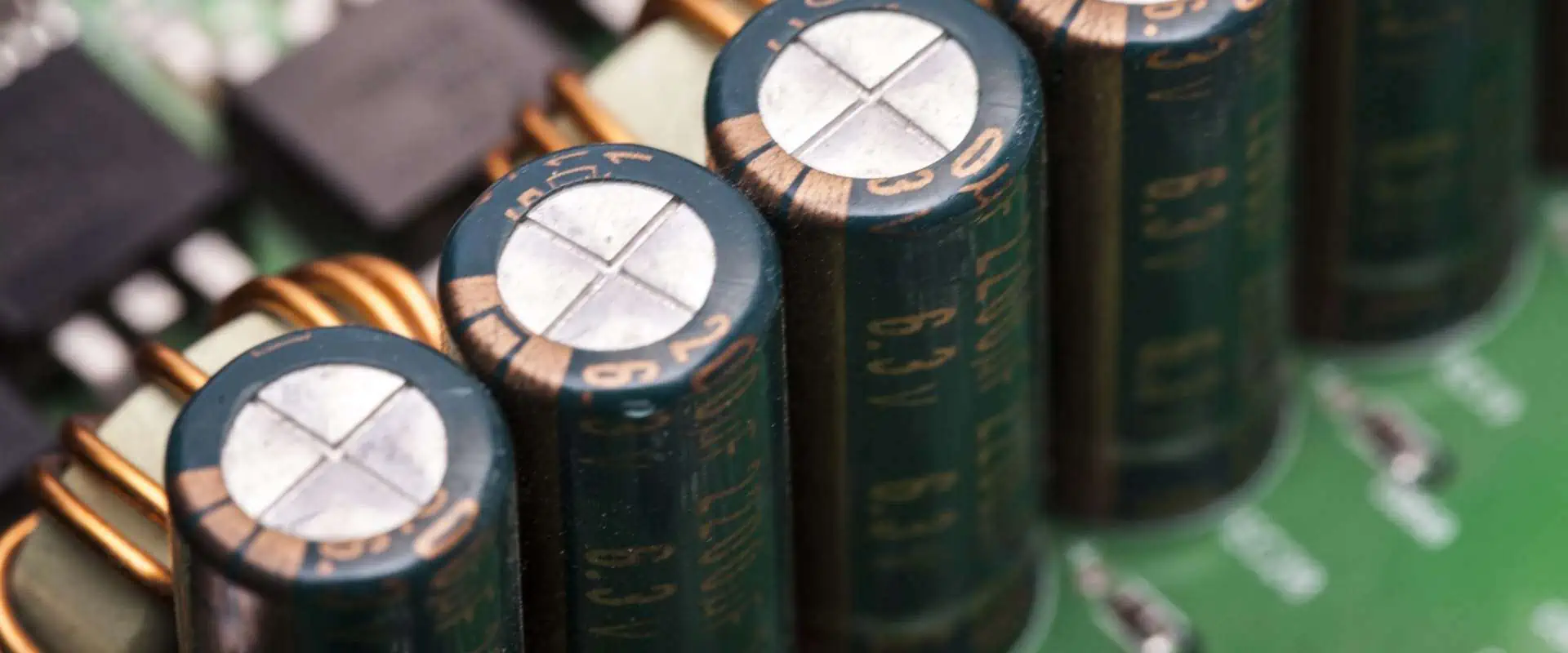
In addition to the capacitor on the Board, separate capacitors may also be included. This may work as a group of bundled capacitors. This is appropriate since it may be used to build a distribution system for your premium design.
PCBs have a similar purpose as capacitors. This is due to the possibility that capacitors might be built of two metal objects that are held apart by a non-dielectric substance. So, a capacitor that may disrupt frequency oscillation should be created by mixing PCB components, connectors, pads, and tracks.
Apart from that, grand planes and power provide the required decoupling capacitance. Even the edges of the PCB can be used as capacitors. Only two excellent copper planes are required. These would act as capacitors. After that, we may proceed to couple discrete capacitors with the PCBs capacitor. This could perform similarly to lumped capacitors, something you’ll use to build a distribution network for your design.
We frequently employ capacitors that are different from those constructed in a student’s classroom while designing PCBs. You must be aware of the various characteristics of the different kinds of capacitors before designing the PCB. This will support both the planning and the design processes.
You may select capacitors utilizing the design libraries if you’re dealing with through-hole and surface-mounted designs. This decision is made on the basis of many characteristics, including capacitance, temperature coefficient, dielectric type, nominal value tolerance, and rated voltage.
The surface-mounted technique has displaced through-hole installation as the more common mounting method. Yet, for some particular applications, drilling holes and anchoring component leads axially or radially via the board will be beneficial. Anytime components are put under mechanical and environmental stress, dependability is required for industrial, military, and aeronautical applications. The several THM capacitor types include tantalum-coupled ceramic discs, silver mica, plastic film, and polarized electrolytic kinds.
Surface mount (SMT) capacitors are devoid of layer-through hole drilling. Moreover, they will immediately mount to the PCB’s surface. The vials take the role of through-hole wires, allowing a conducting link to be made between the layers of the circuit boards. The Surface-Mounted Technique capacitors are mounted on the board’s each side. Comparatively speaking to through-hole mounting capacitors, they likewise feature compact packaging. Multilayer ceramic, mica, tantalum, film capacitors, and electrolytic, are some of the varieties of SMT capacitors.
Circuits often use capacitors, which are widely recognized passive parts. They are a lot like resistors. An electrical charge may be stored by capacitors. They provide many choices as well. The circuit design is what determines this. The amount of energy or charge that a capacitor can store is determined by its capacitance.
Capacitors are typically composed of two sheets including an insulator sandwiched in between. The dielectric material is this insulator. There are several types of capacitors. They may serve a number of functions and are made of various dielectric materials.
Farads are used to measure capacitance. This particular device is rather big. It is typically utilized in picofarads or microfarads because of this. Furthermore, capacitors can be electrolytic or non-electrolytic. The circuit allows for any potential direction of connection for the former. You must correctly position the electrolytic capacitors when mounting them on the circuit. Only one of them is a positive wire, whereas the other one is negative. It’s possible that the placement of such electrolytic capacitors will prevent your circuits from working properly. They could even pop as a result.
There are several uses for capacitors. Digital electronics play one of their crucial responsibilities. The microchips are shielded from the noise here. They are frequently used with circuit devices and capacitive sensing in flashes and lasers because they can rapidly discharge the entire charge they contain. Capacitor-equipped circuits frequently exhibit frequency-dependent behavior. They can be used on circuits that amplify some frequencies because of this.
Like resistors, you may add capacitors in series or parallel. The computation, though, is exactly the reverse of what was done for the resistors. Components connected in series have the same node. Also, whenever the connection is made in parallel, both nodes are shared. If you wish to find the resistance’s total value, sum the resistors that are linked in series. If you require the capacitance’s entire value, you must also include capacitors that are connected in parallel.
Selecting Flux Capacitor PCB Components For Your PCB Design
In this part, we’ll walk you through the factors you should take into account when choosing electronic components for your PCB, like capacitors.
It will always be difficult for new PCB designers to select the appropriate electronic components. The inappropriate component selection might result in the PCB malfunctioning, failing completely, or operating undesirably.
While picking an electronic component during the stage of design, PCB designers need to take into account a number of crucial factors depending on the type of component. You will learn about key factors to take into account while selecting the primary electronic components in this part.
Many circuits make use of capacitors. Across the majority of instances, selecting the capacitor component for the PCB design employing simply the capacitance value is frequently insufficient. The components in capacitors have tolerance factors much like those in resistors. The actual capacitance of a capacitor component varies. This is determined by the manufacturing procedure, DC biasing, operating temperature, and aging.
Consequently, while selecting the electrical component for the capacitor, the capacitance tolerances must be taken into account. Moreover, there is a sizable price difference between capacitors with both low and high tolerance. However, if cost is not a concern for you, we suggest that you select a capacitor with a tolerance of less than 10%. It is adequate to have a tolerance of 10% or 20% for nearly all low-power circuits.
What Value Of Capacitance Will You Get with Flux Capacitor PCB?
If the voltage is stressed or is greater than planned, your capacitor might be damaged. Capacitors are often wired in series with a subcircuit, an output, or another circuit. Your capacitor’s anticipated voltage loss should be estimated or known. We advise that the voltage buffer ought to be 50% more than the anticipated voltage loss. This implies that if you anticipate a 10-volt reduction in voltage over the PCB capacitor, you should select a capacitor with a 15-volt or higher rated voltage.
The duration during which the capacitor is in good condition and provides capacitance in accordance with its intended use is known as its lifetime or capacitor life. It is obvious how important this is, particularly for the electrolytic capacitor. The maker of a product will typically include the lifespan of a capacitor under normal operating circumstances on the product’s datasheet.
The operating temperatures vary for the capacitor. This needs to be seen similarly to resistors. For advanced designs, it is necessary to consider the operating frequency according to the application kind, ripple power, and ECR value.
Conclusion
Be aware that decoupling provides a store of energy that may be used to assist smooth out voltage if there is a variation in the quantity of current drawn. Because of inductance, it is typical for the power supply to wait a little while before responding to the value of voltage. The decoupling cap must thus close this gap. Ensure that it is closer to the electronic chip in order to do this. Otherwise, the lead’s inductance might cause problems rapidly and make it difficult to obtain extra current quickly.
The HDI board, made for low-volume customers, is a compact board with a critical distinguishing feature of high wiring density compared to standard printed circuit boards. This difference between the two types of boards is mainly manifested in the given four aspects.
HDI PCB 1-step & 2-step, & 3-step
The initial step is pretty straightforward, with easily manageable procedures. However, the subsequent 2-step process becomes more intricate and presents several challenges, including counterpoint, perforation, and copper plating issues. Numerous two-step layouts exist, such as staggered positioning of each layer. This design allows connecting the adjacent coating to the intermediate layer via a wire equal to 2 first-order High-Density Interconnects (HDIs).
The second point is that 1st order vias intersect, resulting in a second-order effect achieved through superposition. Although the process is identical to first-order vias, several technical considerations require special attention, as discussed earlier.
The third step involves drilling from an outer coating to the 3rd coating or even the n-2 coating, which is a more challenging process than the previous steps due to the complexity of the hole. A similar approach can be analogized to the 3rd order.
HDI PCB Board Laminate Structure-Blind and Buried vias-3
The commonly printed circuit board is made of fr-4, a combination of epoxy resin & electronic-grade glass fabric that is pressed together. In traditional HDI boards, the outer layer typically uses adhesive copper foil because the laser drilling cannot penetrate the glass fabric. Therefore, non-glass fiber adhesive copper foil is often used instead. However, with the development of laser ablation, it is now possible to penetrate 1180 fiberglass fabric, making the materials used in HDI no different from those used in standard PCBs.
1. HDI PCB – Smaller and Lighter
HDI PCBs have a core board that starts with a traditional dual-sided board and is then laminated with layers continuously. This method of layer accumulation is also known as BUM. When we compare it to conventional panels, these boards are “thin, light, small, and short,” providing several advantages.
HDI PCBs achieve interconnections between layers through conductive through-holes, buried vias, and blind vias. Unlike ordinary multilayer printed circuit boards, HDI boards (circuit boards) are made with massive no. of micro-bury holes.
Unlike standard PCBs drilled mechanically, HDI PCBs are prepared using lasers. This enables an increase in the number of layers & aspect ratio of the HDI PCB
The high density of HDI PCBs is primarily evident in the density of holes, lines, and pads, as well as the thickness of interlayers.
HDI PCBs incorporate micro-through vias, including blind holes & another micro-via design. These designs exhibit two main features. Firstly, they involve hole-forming and micro-hole technology with diameters of at least 150 micrometers. Secondly, there are high demands on cost, production efficiency, and precise hole control. In multilayer PCBs, only pHTs are used, without tiny blind holes, as found in HDI PCBs.
HDI PCB manufacturing requires the improvement of line spacing and line width, which is reflected in increasingly strict requirements for wire defects & surface texture. Typically, the line width & line spacing do not exceed 76.2μm.
The thickness of pads on HDI PCBs is characterized by a density of more than 50 welded joints/square centimeter.
Thinning the dielectric substance is a critical aspect of HDI PCB manufacturing. This is mainly reflected in a trend toward reducing the density of the interlayer to 80 micrometers or below, with increasingly stringent requirements for thickness uniformity. This is particularly important for high-density plates & packaging substrates that require precise impedance matching.
3. HDI PCB with Better Electrical Properties
HDI PCBs not only enable more compact end-product layouts but also deliver more standards of performance & efficiency simultaneously.
HDI PCBs offer a higher interconnect density, resulting in improved signal strength & increased reliability compared to traditional PCBs. Moreover, HDI boards provide better protection against EMI, RFI, thermal conduction, and static discharge issues. HDI manufacturing also employs advanced DSP technology & a range of patented techniques, enabling the boards to handle a variety of load capacities and possess strong short-time load abilities.
Based on the information presented above, it is evident that HDI circuit boards outperform ordinary PCBs in terms of both volume & electrical performance. However, as with any high-end printed circuit board manufacturing process, HDI PCB manufacturing requires a higher threshold of expertise and involves more significant process complexities than the ordinary printed circuit board. Consequently, several issues require careful attention, particularly burying and plugging holes.
The most challenging aspect of HDI production is burying and plugging holes. Failure to adequately perform this step can lead to significant quality issues, such as uneven board borders, inconsistent dielectric thickness, pitted pads, and other related problems.
If the surface of the circuit board isn’t flat and there are depressions, it can result in a phenomenon known as “beaching.” This, in turn, can cause defects such as broken lines, line gaps, and other related issues.
Signal instability may occur as a result of fluctuating characteristic impedance caused by the uneven dielectric thickness.
When the pad surface is not even, it can result in poor packaging quality and loss of the component.
It is important to note that not all board factories can excel in producing HDI boards. However, Next printed circuit board has been dedicating its efforts to this field for over 15 years. Presently, RayPCB has developed its own comprehensive HDI system, with the entire manufacturing process being conducted in-house. The company has invested heavily in acquiring advanced equipment and adheres to stringent standards for Acceptable Quality, such as IPC2, which ensures high reliability. For instance, hole copper thickness is maintained at a minimum of 20μm.
As a business owner, it’s crucial to have essential resources, including money. However, high quality is vital, especially for critical components like PCBs.
Numerous factors contribute to the final cost of circuit boards. To achieve a low-cost printed circuit board assembly, it’s essential to consider these factors carefully.To assist with this process, we have created a helpful guide to provide guidance and support.
Keep reading for 15 tried-and-true tips on how to obtain affordable PCB assembly.
1. Source PCBs from Reliable and Perfect Supplier or Location
The cost of PCBs largely depends on where you purchase them. Typically, PCBs are more expensive in Europe & America, making them more cost-effective for manufacturers in Asia, particularly in China. This can result in significant cost savings when purchasing PCBs.
In addition to cost savings on the actual PCBs, purchasing locally can also help you save on shipping costs that would have been incurred through importing from overseas. Additionally, working with a PCB creator in your area can result in more effective communication & negotiation, potentially leading to lower custom printed circuit board costs.
Many Chinese printed circuit board manufacturers offer fast delivery times, often guaranteeing expedited orders within 24 hours and general orders within 2 to 3 days. It can result in major savings, as it ensures no project delays.
Finding a low-cost and reliableprinted circuit board service provider is essential. Fortunately, there are several PCB manufacturing options available, beginning from the layout stage. However, the type, number, & complexity of elements used can still impact the overall cost of PCB fabrication. Below are some tips for achieving cost-effective PCB design.
3. One sided SMT Components
A printed circuit board price estimator will indicate that circuit boards with SMT elements on both sides are more expensive than those with components mounted on just one surface. One-sided printed circuit boards require only one iteration of pick & place setup rather than two, resulting in lower stencil costs.
4. Label Components in Proper Manner
The aim of component designers is to know the various components used in the PCB. Clear and visible designators placed near the related parts make the setup procedure more accessible and more efficient, thereby reducing costs. Proper labeling assists in preventing errors in manual positioning that could result in additional expenses.
5. Panelize PCBs/Circuit Boards
If you’re producing many PCBs, you should provide them in panels. This increases efficiency & reduces manufacturing costs. Placing many repetitions’ of a printed circuit board on a single panel reduces surface mount technology (SMT) setup time, making it easier for the pick & place machine to pick & put components during printed circuit board assembly runs.
6. Consider the size of board small
PCB size can significantly impact the production cost. While a larger PCB may be more accessible to route, it is also expensive to create.
There are ways to decrease the price of printed circuit board production, particularly in the assembly procedure. One option is to modify the specifications of the circuit board and associated content. For example, selecting PCBs with less than fourteen layers can help lower costs.
Additionally, you can reduce the cost of PCB production by modifying the specifications of the printed circuit board and related product content. For example, choosing PCBs with fewer than fourteen layers can be a cost-saving measure. It’s also advisable to maintain the circuit board thickness board above 1 millimeter and use standard materials such as FR4. Finally, avoiding tiny passive packages can also help cut down costs.
8. Choose the arrangement as complete consignment
Choosing a consignment arrangement means that a intermediary agrees to sell things owned by the original owner. Consignment has several advantages in the case of SMT and PCB assembly. This can help reduce the costs of PCB production as the consignee is responsible for purchasing and providing components, reducing the burden and prices on the consigner. Choosing consignment for your PCB needs can bring you some benefits, one of which is better pricing compared to buying from retailers.
With consignment often available online, you can save time & money by avoiding the need to go from one store to other store physically. Instead, you can conveniently browse available options on your computer, select the best costs, and add them to your shopping cart.
9. Take help and advice from Experienced Suppliers like RayPCB
Building a strong connection with your PCB supplier can be beneficial when looking for low-cost printed circuit board assembly options. Experienced suppliers have extensive industry knowledge and can suggest where to find excellent deals on SMT components.
When finding low-cost circuit board assembly solutions that don’t compromise quality, consider contacting your established PCB suppliers for advice. You should contact several suppliers to get a neutral viewpoint and choose a supplier that prioritizes your interests. This approach can help ensure that a pick & place machine can easily handle the circuit board components during assembly.
Finding high-quality printed circuit board assembly at the most affordable price often starts with an online search. Nowadays, numerous electronic websites provide valuable information on where to find the manufactured goods you need at a reasonable rate. It’s essential to make some comparisons before manufacture a purchase decision. This involves browsing through different stores to select the one that offers the most excellent price.
Before placing an order with a PCB manufacturer, it is essential to review the features & specifications of their products carefully. Additionally, it is helpful to read reviews from previous customers on the producer’s website to get an idea of their reputation and the quality of their products.
11. BOM File Designing
The BOM is not just a simple list of elements. It’s crucial to ensure that the components are placed on the correct footprint on the PCB. A reliable PCB assembler can also recommend approved sellers who can provide the parts listed in your Bill of Materials at more affordable prices.
An accurate Bill of Materials (BOM) is crucial for planning and budgeting your procurement. This lets you take advantage of quantity discounts and better manage component usage. To ensure that your Bill of Materials list is always precise, it’s a good idea to spend in the best-printed circuit board design software. Additionally, a clear BOM can also assist you in identifying authorized vendors suggested by the PCB assembler who can supply the parts on your BOM at better prices.
12. Right PCB components for Low Cost
The kind of elements you choose plays a crucial role in determining the overall printed circuit board assembly cost. Therefore, it’s essential to stay advanced with the latest information on available parts in the market. While it’s tempting to opt for the newest memory chips/MCUs, you should also consider their availability & cost.
Avoid rushing for highly complicated components that may cost you luck. There are more cost-effective alternatives that can still meet your needs. Additionally, make sure to buy elements from less expensive sources. If possible, consider using in-house components.
13. Make sure to adjust the batch and order quantity online
When wanting to save money, it is always advised to buy more, especially for significant projects. To achieve this, it’s good to seek a corporation that can create many printed circuit boards simultaneously.
If you have a small project, it’s best to look for a printed circuit board assembler that specializes in producing prototype printed circuit boards or smaller creation quantities. Such businesses are more likely to offer you competitive pricing, even for low-volume production runs.
Keep track of your printed circuit board needs depending on low and high seasons, and adjust the order quantity accordingly to avoid shortages/wastage. This will help you to optimize your costs and keep your inventory in check.
14. Search for best PCB maker
Choosing a one-stop PCB company can help you avoid additional expenses from contracting multiple printed circuit board producers to assemble your PCBs. This includes shipping expenditures.
With a one-stop company, you can get rid of these costs and enjoy multiple services under one place, including PCB fabrication, design software, assembly, & shipping. A PCB assembler that offers a comprehensive service can provide a quote that includes all costs, avoiding unexpected additional fees.
15. Keep up Quality & Cost
One of the advantages of opting for cost-effective SMT in printed circuit board assemblage is that you can get quality & functionality without overspending. The key is to procure high-quality substances from reliable sources. This ensures that your end products are dependable and long-lasting while still allowing you to save on production prices.
Initially, low-quality things may appear cheaper, but the issues they reason in the long run can result in significant expenses.
Summary
Achieving low-cost printed circuit board fabrication & assembly is not an easy task, but it can be done with intelligent sourcing of printed circuit board components & design strategies. It is essential to find ways to reduce complexities that increase unnecessary costs.