The STM32 is indeed a development board with outstanding performance and a ton of functionality in a compact design. It contains a 32-bit ARM Cortex M3 CPU, flash storage of 64Kbytes, and SRAM of 20 Kbytes, all operating at 72MHz. It offers a wide variety of peripherals and I/O, including one PWM stopwatch, many high-resolution ADC, and multi-channel DMA. Also, it features several communication interfaces, such as USB, three UARTs, two I2Cs, and two SPIs. Moreover, it allows the board to be soldered with SPI Flash and enables the installation of more flash.
Features of Stm32 PCB Design
You can provide the circuit power source and USB connection using the onboard Micro USB interface.
LED test indication on board
Integrated power LED and reset button
Onboard 3.3V 100ma Regulator
The ids of all pins are indicated, and GPIOs are brought out.
You may immediately insert the circuit over the breadboard after the headers’ soldering.
Do you need a detailed manual for coding STM32 microcontrollers? In that case, you’ve found the proper site! STM32 microcontrollers know for their cutting-edge features, adaptability, and affordability. We will outline a step-by-step procedure for programming an STM32 microcontroller in this article. Also, we will go through the advantages of utilizing STM32 microcontrollers, their coding fundamentals, programming hints, and typical programming problems. Eventually, we’ll provide you with a few courses to support your beginning. So let’s start right now!
Let’s start by providing a definition for an STM32 microcontroller. STMicroelectronics produces a particular kind of microprocessor known as an STM32 microcontroller. It is constructed using the 32-bit ARM Cortex-M CPU. Automotive, medical, consumer, and industrial electronics are just a few of the industries that utilize STM32 microcontrollers. They possess the feature like cutting-edge features, adaptability, and affordability.
STM32 microcontrollers have the ARM Cortex-M microprocessor in addition to other cutting-edge capabilities like
Several peripheral devices, including timers, analog-to-digital converters, and communication interfaces.
A large array of tools for software development that simplify programming.
Low consumption of power
enhanced performance.
STM32 microcontrollers are a great option for many applications because of their qualities.
Benefits of Using Stm32 PCB Design Microcontrollers
Let’s talk about the advantages of utilizing STM32 microcontrollers as you are aware of what they are. The affordability of STM32 microcontrollers constitutes one of their main advantages. They may be utilized in many different applications and are significantly less expensive than some other microcontrollers.
STM32 microcontrollers are inexpensive and offer a variety of software and peripherals development tools. They may thus be easily customized and are quite adaptable. They are also suitable for battery-powered devices due to their low consumption of power. The high-speed functionality of STM32 microcontrollers also qualifies them for devices that need quick processing.
One # step: Connect The Dev Board To Your Computer
The proper STM32 development circuit board must be chosen for your program during the initial stage. Use the ST-LINK downloader to connect the board to the computer. You have to take into account elements like size, price, features, and performance. STM32f051k8u6 is a supposed example.
Two# Step: Download STM32CubeMx And Kiel5 Tool Kits
Visit ST’s official website or the Link below to download the “STM32CubeMX” program.
Three # Step: Create A New Project In A STM32CubeMx
Click twice to launch “STM32CubeMX.”
Choose “New Project” from the menu
Using the MCU Filters, Then choose the desired board or MCU
Four # Step: Install New Libraries For STM32 Development Board
Download the stm32f051k8u6 library by selecting “Help then Install New Libraries
After downloading, choose “stm32f0,” and then click the button “Install Now.” The box becomes green.
Five # Step: Generate The Code And Save The Project
The act of producing C or C++ code entails creating the microcontroller’s instructions. An Integrated Development Environment (IDE) like IAR, Keil, or Eclipse is used for this. Of course, another option is to create the code using STM32CubeMX.
Save the task:
Type the name of the project into the “Project Name” field
Choose the project and then save it to the “Browse” disk directory;
Choose to produce the “Toolchain / IDE -> MDK-ARM V5” software project for Keil5;
Create the project and choose “OK.”
Six # Step: Compile the Program Code In Keil5
After writing the code, it has to be compiled. The process of putting the code together into a type of format that the microcontroller can read is known as compilation. Here, the procedure is completed using Keil software. We first click “Open Project” to access the STM project we saved in the previous step:
Next, select “build” or hit the “F7” key to finish the project compilation.
Seven # Step: Debug The Program Code With Vision Debugger
The Keil5 Vision® Debugger is used for debugging the STM32 development board’s program code. It offers an array of test features, including “Event Statistics,” “Execution Timing,” “Performance Analyzer,” “Event Recorder,” and “Component Viewer.”
Eight # Step: Upload The Program Code To The STM32f051k8u6 Dev Board
To finish the programming, click the button “Download” or hit “F8” on the keyboard.
Tips for Programming Stm32 PCB Design Microcontrollers
After acquiring programming skills for the STM32 microcontroller, let’s explore some programming tips. One key recommendation is to utilize the STM32CubeMX tool, which facilitates microcontroller configuration, code writing, debugging, and code uploading.
Another tip is to implement a control system to streamline the tracking of code revisions and ensure their up-to-date status. Additionally, it is critical to perform comprehensive testing of the code before uploading. This practice will allow the detection of any errors and guarantee that the code performs as anticipated.
Common Programming Issues
Debugging can prove to be a challenging task as it demands ample patience and a great deal of experimentation. It is crucial to utilize the debugger that is compatible with an STM32 microcontroller & conduct thorough testing of your code before uploading it.
Memory allocation stands as another prevalent concern when it comes to microcontrollers. It is the act of assigning memory to a microcontroller, which can prove challenging as it necessitates ensuring that there is sufficient memory available for both the code & data. Employing memory allocation equipment can be beneficial in facilitating the correct allocation of memory.
Comparison of Stm32 PCB Design with ATmega328
Having experience working with AVR-based microcontrollers such as the ATmega328, it’s more convenient to draw comparisons with the STM32. STM32 microcontrollers are generally more expensive than the ATmega328; they boast significantly higher memory & RAM. Additionally, the STM32 provides a wide range of chips, from low-cost options to more influential ones. With increased memory & storage, developers have greater flexibility in making applications and can expect faster operating speeds.
STM32 has another noteworthy advantage in the form of its abundant GPIOs and peripheral support. It supports various communication protocols, such as LIN, I2C, USB, I2S, SAI, IrDA, and many more. Furthermore, STM32 is extensively utilized in devices, particularly smartphones, tablets, and smartwatches. Leading tech giants, including Apple, Qualcomm, Nvidia, and Samsung, have adopted the STM32 as the foundation for their products.
Migrating from Arduino to Stm32 PCB Design Microcontrollers
Hardware Layout
Although Arduino is an excellent platform for gaining proficiency in electronics and creating preliminary prototypes, it’s usually impractical for some commercial products. If you want to know how to transition from an Arduino to an STM32 microcontroller, learn about the necessary steps.
Arduino’s platform has significantly reduced the obstacle to entry for hobbyists & startups to create their embedded devices.
The wide variety of production boards, straightforward programming & uploading interface, and expansive community support make Arduino an appealing first choice for product developers.
As project requirements expand and evolve with time, an Arduino platform may start to impose limitations.
One of the main factors contributing to this limitation is the narrow range of available hardware options, which is due to the substantial effort needed to seamlessly integrate the commercial microcontroller with the Arduino software.
Most Arduino microcontrollers utilize 8-bit AVR microchips, which have limited CPU performance capabilities.
The performance drawbacks are amplified by the reality that the Arduino platform prioritizes portability and simplicity over fully optimized low-level configuration, resulting in much of the configuration being concealed from the user. As a result, software running on an Arduino is unlikely to be fully optimized.
Due to these factors and others, when there is a need to enhance the performance & flexibility of an embedded device, it’s typically necessary to transition away from the Arduino platform. Instead, a large proportion of industrial embedded systems employ 32-bit ARM chips, which power devices such as modern automobile computers & various others.
When it comes to balancing price and performance, there are no chips that can match these; the ARM processors have been a consistent feature of computing for a long time, with no indications of losing their popularity.
The STM32 series of microcontrollers is a highly sought-after alternative that preserves many of the attractive features of an Arduino platform. With the ability to reach CPU speeds of up to 550MHz and an extensive range of available chips, they unlock a vast array of new possibilities.
Conclusion
This blog post covers a comprehensive guide on programming STM32 microcontrollers. It encompasses the advantages of utilizing STM32 microcontrollers, fundamental concepts of programming them, suggestions for programming, and prevalent programming problems. Additionally, it covers the top development boards for STM32 microcontroller programming and suggests courses to initiate your learning journey.
In this blog, we will assist you in configuring the ESP-IoT-Solution development environment. Following that, a straightforward example will demonstrate how to set up a working environment, establish a project, compile and upload firmware onto the ESP32/ESP32-S series board, and do other tasks using ESP-IoT-Solution.
Introduction to ESP IoT Solution
The following elements are mostly available in ESP-IoT-Solution, which may be useful as an additional part of ESP-IDF to enable easier development. It comprises code frameworks and peripheral drivers typically used within the Internet of things system development.
Device drivers for things like sensors, audio devices, screens, actuators, input devices, and more. Code structure and relevant documents for things like security encryption, minimum power management, storage, and other stuff. Entrance instructions for Espressif’s fully accessible solutions are out of view of actual use.
To begin using the ESP-IoT-Solution, simply select a development board mainly from ESP32/ESP32-S family, or choose a supporting board straight from the Circuit Boards Component for a rapid start.
The following functionalities are supportable by ESP32/ESP32-S family SoCs:
Wifi at 2.4 GHz
Bluetooth
A powerful single-core or dual-core Processor that has the ability to operate at 240 MHz
Coprocessor with extremely low power
GPIO, I2S, I2C, SPI, UART, RMT, SDIO, LEDC PWM, TWAI®, Ethernet, USB OTG, Touch, and other peripherals are among them.
Extensive memory resources, comprising external PSRAM compatibility and internal RAM of approximately 520 KB.
Support security features, such as hardware encryption.
The 40 nm-designed ESP32/ESP32-S line of SoCs exhibits the finest RF performance, power and adaptability, and dependability in a wide range of device and power settings.
ESP IoT Reduces Cost & Complexity Of IoT Devices
Nowadays, cloud connection is a hot topic, especially considering its many benefits, such as:
Enhanced device accessibility with Cloud connectivity;
Improved backup choices for important data;
Because of Over-The-Air updates, device security has been strengthened, and maintenance costs have decreased;
Enhanced productivity brought on by automation and enhanced device collaboration.
The technology is being extensively adopted across many industries thanks to these well-known benefits, to the point that almost 60% of organizations presently employ IoT, with just 9% of companies currently experiencing no IoT at all. IoT enthusiasts still face obstacles, which include the price of deployment and the incorporation of IoT using current technologies.
Espressif’s response to the IoT technology integration challenges and ensuing development expenses is ESP-Hosted. ESP-Hosted is an open-source approach that operates off-the-shelf, requiring little or very little modification to current technologies and reducing development expenses.
More specifically, ESP-Hosted provides a method for leveraging Espressif SoCs plus modules as telecommunication coprocessors. This approach gives the microcontroller, or host microprocessor, wireless connection like Bluetooth and wifi, enabling it to interface with some other devices. ESP-Hosted connects well with the host CPU via one of the widely used peripheral interfaces, such as UART, SDIO, or SPI.
The following benefits may be obtainable from this approach, which isolates the wireless connection module first from the primary host-processing module, by adding wireless capabilities to current MPU/MCU-based solutions:
· Faster Development Cycles
ESP-Hosted enables the connection module to operate over an 802.3 interface which is ESP-Hosted-NG, or the common 802.11 interface, which is ESP-Hosted-FG. In this manner, ESP-Hosted performs like a plug-and-play gadget.
· Reduced Re-Qualification
The bulk of a developer’s program does not need certification since installing the connection module doesn’t really affect user-space applications by ESP-Hosted.
· Power Saving
The primary MCU/MPU can continue to operate in a low-power state while still being interlinked with the network. As a result, only real activities, such as outsourcing all connecting overheads to a connecting module, require involvement from a main host.
· Easier Upgrades & Product Variants
Developers may create numerous iterations of an identical product with various connectivity options thanks to the design, which makes it simple to change the wireless connectivity of their goods. In the example below, the developer may utilize the very same Host programs and tools while choosing from a range of internet connectivity choices, including wifi 4, Wi-Fi-6, and Wi-Fi-6 dual.
To facilitate developers’ use of the numerous ESP32 functionalities, Espressif has developed the program code of the ESP-Hosted publicly available. Further useful to developers are the HMI and IO features of ESP32-S3 and ESP32, as well as the sophisticated security abilities of ESP32-C3 or the device’s Digital Signature Peripheral. As a result, the options are unlimited.
There are two versions of the ESP-Hosted solution: ESP-Hosted-NG and ESP-Hosted-FG. The kind of network interfaces given to the hosts and the configuration/control of wifi over the ESP SoC/module distinguish them from one another. Each variation has its own firmware software and host.
· ESP-Hosted-FG
This type gives the host a typical Ethernet interface of 802.3 standards. The following options are provided to the host so that they are able to do this:
a straightforward Ethernet interface of 802.3 standard, which is a network interface;
a simple control interface that helps in setting up wifi only on ESP SoC;
An HCI interface that is standard.
This method is perfect for all MCU hosts since it uses straightforward 802.3 interfaces. While utilizing this AT firmware-based method or when integrating the complicated 802.11 interfaces, the MCU program can keep taking advantage of the industry-standard TCP/IP stack as well as prevent substantial modifications to the host application.
· ESP-Hosted-NG
This variation adopts a conventional strategy while giving the host a type of network interface, making it especially intended for hosts that especially run the Linux OS. This enables the usage of ESP SoCs/modules with common wifi programs like wpa_supplicant. These benefits are provided by this answer:
a Linux host’s 802.11 standard network interface, a type of common wifi interface;
Under Linux, the cfg80211 standard interface is provided for wifi setup;
As previously noted, the Tensilica 32-bit CPU powers the ESP32. This employs one or two cores. The performance is in the range of 600 DMIPS, and the frequency of the clock is over 240MHz. Also, even in a deep sleep state, its low-power use enables ADC conversions, calculation, and leveling of the threshold.
2. External SRAM
For the protection of developers’ software and data, ESP32 enables a maximum of 4 16MiB auxiliary SRAMs and QSPI flashes. The high-speed cache is used to access the exterior QSPI flash drive and SRAM.
3. Security
The security aspects of the IEEE 802.11 protocol, including WFA, WAPI, and WPA/WPA2, are supported. ESP32 also features a secured boot and storage encryption.
Functions of ESP IoT
Whenever it applies to the IoT, ESP32 has various uses. Just a few IoT uses for the chip include the following:
Networking: The module’s dual-core processor and wifi antenna allow integrated devices to communicate with routers and send data.
Data Processing: Processing simple inputs from digital and analog sensors to much more complicated calculations using a Non-OS SDK or RTOS.
Utilizing IoT P2P networking, direct communication is established between various ESPs as well as other devices.
Web Server: Access HTML- or development-language-written pages.
Applications of ESP IoT
The following are some major IoT devices frequently contain ESP32 modules:
Intelligent industrial equipment, such as PLCs.
Wearable health monitoring devices are among the smart medical equipment.
HVAC systems and thermostats are examples of smart energy gadgets.
Smart security equipment, such as smart locks and security cameras.
Chip Versus Module Versus Development Boards
The chip has no other name than ESP32. The format in which device makers and developers choose to purchase this is one of three options, and their choice will rely on the specifics of their situation:
· ESP32 Chip
Many Companies make this basic chip. It is unshielded and requires soldering to be connected to a board or a module. Because doing so would make the manufacturing process even more difficult, the majority of device makers do not merely buy chips.
· ESP32 Modules
The chip is housed in some type of surface-mountable module. The advantage of buying a module comprises that throughout the manufacturing process, they may be quickly installed onto an MCU. Device makers don’t have to worry about including extra steps in the process of production to meet FCC compliance in regard to wifi shielding.
· ESP32 Development Boards
The IoT Microcontroller development boards with modules already installed using the ESP32 chip. Before going into mass production, enthusiasts do the tests and prototypes of IoT devices, device makers, and developers. ESP32 microcontroller development boards come in a wide range of types and models from various vendors. While selecting an appropriate IoT ESP32 microcontroller development board, keep the following crucial specifications in mind: ADC pins, LEDs, shielding, wifi antenna, flash memory, and GPIO pins.
There are many reasonable alternatives with ESP32 modules and boards, as the comparisons above demonstrate. We’ve included the most popular ones below to aid you in making a selection.
· ESP32-WROOM-32D
The ESP32-D0WD interacts with this ESP32 module that is quite popular. The ESP32-WROOM-32D’s flexibility is the major factor in its popularity. It may be useful for a range of applications, from voice compression as well as music streaming to sensor networks.
Mostly, ESP32-WROOM-32D and ESP32-WROOM 32U use wrongly in industry. Although the two modules are remarkably similar, the ESP32-WROOM-32U differs from the ESP32-WROOM-32D in that it incorporates a connection of U.FL.
· ESP32-WROOM-32
The initial ESP32 module released by Espressif is the ESP32-WROOM-32. A potent, general Wi-Fi+BLE+BT MCU device is the ESP32-WROOM-32. The chip ESP32-D0WDQ6 seems to be the heart of this device. Scalable and adaptable design features are available in the integrated chip. The ESP32-WROOM-32 is unquestionably a fantastic module, yet we do not suggest it for modern designs.
· ESP32-WROOVER
There are two variants of the ESP32-WROVER available; one includes a PCB antenna, while the other utilizes an IPEX antenna. The ordering details for both variants are available here. The ESP32-D0WDQ6 semiconductor, which is at the heart of this device, is similar to the ESPWROOM32 chip.
Two independently controllable CPU cores are present in this ESP32 device. The clock frequency of the CPU is changeable between 80-240 MHz. The user can also turn off the Processor and constantly check for alterations or threshold crossings using the less-power coprocessor.
· ESP32 CAM
In comparison with the various development boards here on the list, the ESP32 CAM seems to be a bit unique. An inbuilt camera with a miniature SD card slot is another feature of this properly developed microcontroller. As the ESP32-CAM has so far been based on the module of ESP32-S, it has similar features. This offers clock speeds that go up to around 160 MHz, wifi image uploading, 9 GPIO ports, I2C, SPI, and PWM interfaces.
It features a 2 Megapixel sensor-equipped OV2640 module which also accommodates OV7670 cameras. When exploring something like the ESP32-CAM, it can be simpler to forgo a solderless board due to the large number of components being placed on the bottom side. Also, we advise utilizing female Dupont connections with jumpers.
Amazon’s Alexa is the technology that allows you to talk to a computer system by using your voice. This system is connected to the internet and can answer questions, give you weather & sports updates, read news, play sounds from various sources, and do many other things. The device that links to Alexa services is called Amazon Echo.
In addition to its built-in features, Alexa can also work with other devices & services. To access these features, you use voice commands, which are similar to the basic commands.
Companies and manufacturers are adding Alexa to their devices to improve their operations and increase their business.
The Alexa Skills Kit (ASK) SDKs can create new say commands that work with web services or AWS lambda functions to perform tasks. It helps businesses to add a voice interface to their SaaS frameworks or improve their existing business processes by using voice commands.
You can connect to the Amazon Alexa IoT ecosystem by:
Utilize Amazon Echo to send voice to Alexa.
To make Amazon Alexa work with other devices, you must create a set of voice commands called skill sets. Users can use these commands to control cloud-connected devices through their voice using Echo/mobile app. Every skill set is connected with a specific Alexa API that executes the command.
When you talk to Alexa, your voice command is sent to a special AWS lambda program. The program then figures out what you want to do and sends a message to the device’s cloud to do the action. This program and message system is called Alexa API.
The cloud of the device understands the sms and sends a signal to either turn on or turn off.
The Alexa Skills API checks if the message sent to the device’s cloud was successful/not and sent a response message.
Alexa gives the user feedback based on the response received from the device cloud.
Benefits of Alexa IoT
A Gateway can connect IoT devices to perform various tasks in different industries like retail, industrial automation, home automation, automotive, etc
Integrating Amazon Alexa with VOLANSYS’ CENTAURI 200 IoT gateway can provide many benefits to enterprises, such as.
Voice Controlling: By integrating Amazon Alexa with VOLANSYS’ CENTAURI 200 IoT gateway, businesses can benefit from touch-free solutions and advanced capabilities in their operations. Voice control has made IoT( Internet of Things) products smarter & more connected, allowing people to obtain information & control their environment through their tone of voice.
A gateway helps people communicate wirelessly between their device and the user.
Implementations: Most of the businesses like food and drink, online shopping, and more have been promoting ways to order things on your phone. Now they’re taking it further with say-only ordering, you can do using your Android or iPhone. With Amazon Alexa, you can even order things just by talking! It has made a big impact on how things work in real life. The Echo isn’t just helping businesses, it’s also making a big difference in our everyday lives.
You don’t need to be a tech expert using IoT ( Internet of Things )devices safely. Here are some simple tips for keeping your IoT devices secure.
Make sure that the device and router have safe, unique passwords. When you get a new device, it’s important to change the password to something different. If you & your neighbor have the same equipment, you could also have their password, which makes it easier for someone to hack into your device. By changing the password to something unique, you can lower the risk of being hacked.
· Keep the device updated
It’s really important to install updates for your device that become available. Updates often come with security fixes, so they help keep your device safe from hackers. Some devices can update automatically, so you don’t have to worry about it. Also, be careful with equipment that is no longer supported by updates. Technology changes fast, so it’s possible for a device to become outdated and dont get updates sooner than you think!
· Use a debit or credit card
If you’re looking for a safe way to make purchases, a Visa gift card/a reloadable card is a good option. These cards aren’t linked to our bank account, so if someone hacks into the card, they can’t get to your bank account and steal your money.
Don’t link it to your sensitive email accounts. If you connect your equipment to the work email/personal account with sensitive information, hackers could gain access to information that you want to keep private.
Advanced measures of Alexa IoT
If you’re good with technology, you can make your IoT devices more secure by doing these things.
Turn off Universal Plug and Play. This function makes it easy for connected devices to find and talk to each other. But it can also make your device vulnerable to prying hackers.
Connect the device to its wifi network. This method ensures that if a device is hacked, it won’t let the hacker access any other internet-linked device.
Use restriction: This makes sure that the equipment can only talk to the devices that you have permitted.
Future of Smart Homes with Alexa IoT
Amazon thinks that using your voice to control your home is the future, and it will make using technology much easier. For example, you can ask Alexa to play a song or turn off the lights while you’re in the kitchen washing dishes. Nowadays, a smart house isn’t just about using connected applications and your voice to make things easier at home. You can ask for everyday news or even check the traffic while preparing.
Smart home technology has evolved, & with the recent development of voice-activated assistants like Alexa, people realize that having a smart house is easier than they thought.
In the past, it was a hassle to turn on a smart device because you had to unlock your cell phone, open the app, & press the button. It was easier to get up and do it yourself. Plus, you might have had to use different apps for different devices. But with Alexa and voice commands, you can now control your smart devices just by asking Alexa to do it for you. You can ask Alexa to turn on the lights, lock the door, adjust the temperature, or even order you to ride to work.
Regarding Alexa and making homes smarter, we still feel like we’re just starting. But we’re really happy with how many device makers and software developers are creating cool stuff for Alexa & making it part of their products.
Biggest Imapcts of Alexa IoT
Alexa doesn’t just make things easier by letting people control their smart homes with their voices. It’s also really helpful for people who are visually impaired/elderly. Lots of those folks have written to us to say thank you for giving them a way to be more independent; now, they can use their voice to control things around them.
GE is making a new table lamp that has Amazon Alexa built right in. That means you won’t need a separate Echo application to use Alexa – you can talk to the lamp)
Reluctant consumers use Alexa IoT in the smart home
People who are just starting have lots of choices to pick from.
At Amazon, we want to help people turn their houses into smart homes using Alexa. With Alexa, you can control lights, locks, thermostats, fans, and sprinklers. If you want to set up a smart house independently, choose what you want to control and then check the Amazon Smart Home store to seek the products that work with Alexa. It’s easy!
If you use companies like Vivint/Alarm.com for your home services, they can help set up a smart house system that works with Alexa and fits your needs. As people want smarter homes, we’re teaming up with a group called CEDIA, which helps professionals all around the country install and design smart home systems.
Alexa IoT Voice Service
AVS is a set of tools that developers can use for free to add Alexa to their applications. All they need is a speaker, microphone, and internet connection, and with just a few simple instructions, they can integrate Alexa into their product.
GE’s new smart light utilizes AVS to connect Alexa to a modern table lamp. It means that you can light up a room with energy-efficient LED lighting and also access the Alexa features that you would find on an Amazon Echo without needing a separate device.
A new small lamp is coming out that has a special feature. It has a speaker & microphones that work like Alexa, the virtual assistant in Amazon devices. You can use your voice to ask Alexa to read the news, control your other smart devices, and play music.
Overall, adding voice control to smart devices has made it very easy to interact with them at home. We think that when people see how easy it is to turn off a light just by speaking to Alexa, they will want to try using other smart house features too.
How do Alexa IoT Devices Work?
IoT devices are objects that can do different things, but they work in similar ways. They have a computer inside that can sense things in the real world. They use special software and are available together on the internet. To work properly, they need a unique IP address connected to a special server.
To control most IoT devices, you need to use a special app on your phone. This app lets you turn on and off devices like lights in your home. Some devices don’t need an app because they have a built-in server. It means they can work immediately, like when a sensor turns on lights when you walk into a room.
The main thing that makes homes smart and safe is IoT. It means that devices such as sensors and cameras are all connected and can be controlled using a smartphone. It makes it possible to have constant security all day and night.
· Activity Trackers
Cameras that help keep your home safe can send you alerts and make you feel more secure. Activity trackers can sense things about your body and send that information in real time. You use them to check and manage things such as appetite, blood pressure, physical activity & oxygen levels.
· Industrial Security and Safety
You can use IoT technology to detect and monitor restricted areas for trespassers. You can also use special sensors & cameras to check for pressure or leaks of dangerous chemicals. It helps you fix problems before they get worse and cause serious harm.
· Augmented Reality Glasses
AR glasses are special glasses that have a computer inside them. They show you extra information such as 3D animations & videos on top of what you see in real life. The glasses show you this information through their lenses and can even help you use apps on the internet.
· Motion Detection
Motion sensors feel when dams, bridges, buildings, & other big structures shake or move. They can find problems or things that aren’t normal, leading to bad accidents. You can also use these sensors in places where floods, landslides, or earthquakes might happen.
Unlimited Possibilities with IoT
IoT technology is still very new, and it’s expectable to grow a lot in the future. When we combine IoT with AI, we’ll be able to come up with new and creative ideas that can be used in many different industries.
To have a good career in the Internet of Things (IoT), it’s important to start on the right path &check how the Internet of Things works with technologies.
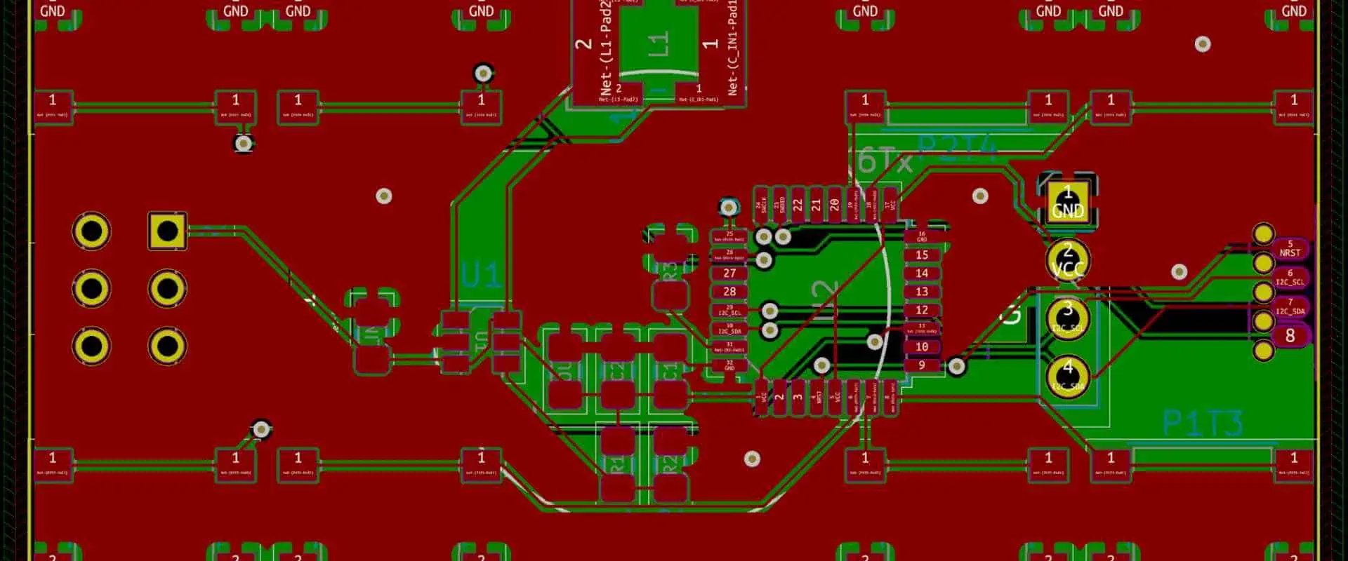
A user-defined region or perimeter included in the design and which copper items cannot intersect is known as a “Keep out” in the design of PCB. A Keepout is frequently used to restrict the region. It utilizes automatic copper placement procedures like interactive routing and polygon pours. It also designates an improper position when copper items are placed manually.
Keepout objects employ the current Clearance Constraint Regulations to regulate routing and identify positioning violations as designated “no go” zones during design layout; however, unlike other inserted objects, they cannot be allocated to something like a Net, nor are they displayed in produced printouts or Outputs. In the most basic sense, a Keepout functions as such an “interference” item that, in accordance with the worldwide Clearance Rule, prohibits other copper items from overlapping its region.
Through its feature of support for Item Specific Keepouts, Altium Designer makes it possible to create and use Keepouts. It is possible to arrange placed Keepout items to only apply to specific types of objects, including tracks, copper regions, pads, and vias, greatly enhancing the efficiency and flexibility of Keepouts.
Cross-hatching displays Keepout items in the Printed Circuit Board Library Editor and PCB. Keepout objects assigned to a Keep-Out Layer. It displays inside the Keep-Out Layer hue. But Keepouts are set to a particular signal layer. It displays in the hue of this specific Layer.
Keepouts are perfect for designating non-routable circuit board areas like mechanically incompatible parts like mounting holes and the edges of a Circuit, high voltage regions, or electrically sensitive, especially exposed copper spots as in Test Points and Fiducials. After particular Keepout Limitations have been given, the flexible nature of Item Specific Keepouts additionally enables them to also be put across other objects. To limit the scope of automatic Via Stitching, a Keep out sometimes puts over already-existing copper sections like a Polygon Pour when it configures to restrict solely via.
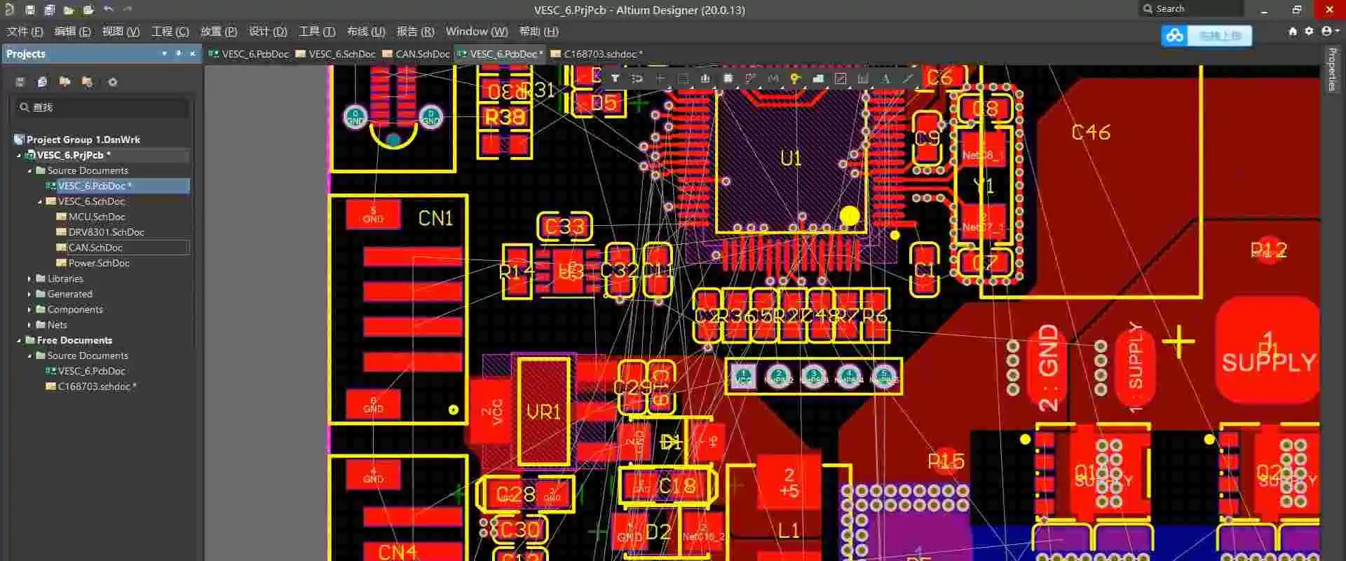
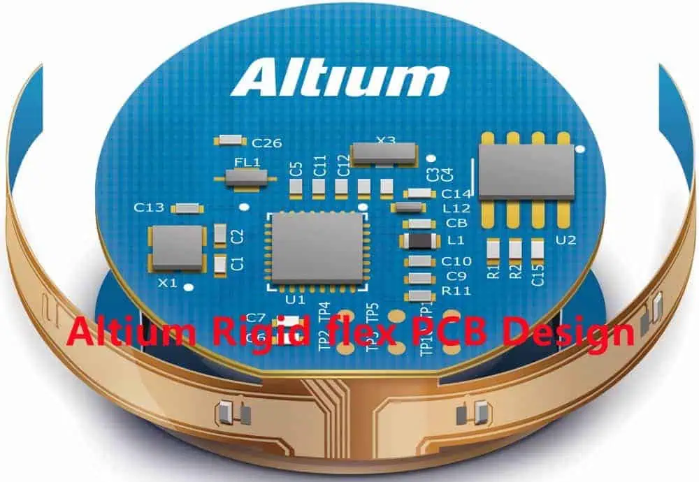
First off, Altium is a comprehensive PCB layout software suite that houses several design tools on one platform. The most recent edition of Altium, Designer-20, is a product of several years of invention and development. It aims at creating genuinely integrated design tools. Because of this, the software enables users to make effective use of all aspects of the PCB design process.
Altium is now among the most used Circuit Board design tools, praised for its superb mix of control and use. A user-friendly interface created by Altium’s creators puts all of the system’s capabilities at their fingertips. Broadly speaking, Altium Designer aids PCB engineers in bringing their imagination to life.
The workspace for Altium Designer consists of two essential parts:
The very first is Altium Designer’s primary content editing location. It appears on the very right side of the program.
The Workplace Panels make up the second location. In addition, some panels spring out from the right side of the tool, most float, while others hide in Altium. Some panels dock on the very left portion of the application.
Placing Altium Keep-Out Layers
Using the Place to Keepout menu, a Keepout is then added to the editor’s design area, where the selected Keepout style, like its Track, Region, Fill, or Arc, is applied to the currently operating Layer. To change the Keepout’s physical attributes, Layer, or item type limitations, choose Properties. These Keep out characteristics are related:
The Keepout Layer is determined by the Banned for Layer, which determines the circuit layer as to which Copper Items are Limited. Choose the Keep-Out Level to create an all-layer keep-out.
Keepout Restrictions specify which object kinds are going to be constrained mostly due to Keepout. By not enforcing the relevant Clearance Rule, deselecting a type of object will result in the Keepout, allowing infractions by that kind of object (which is not specifically kept out).
The following options are available for placing Track Keepouts in PCB and Circuit Library Editors:
Insert a track or trace keep out within PCB Editor using the following methods:
From the main menus, select Location, Then Keep out, Then Track.
In the Active Bar menu, which places at the right top of the layout area, select the button in the drop-down menu for graphic objects. (Hold down a button on the Active Bar for additional related commands. Once the command invokes, It will rise to the top of that portion of an Active Bar.)
Right-click, From a context menu, select Place, Then Keepout, and Then Track.
Insert a track or trace keep out inside the Circuit Library Editor in any of the following methods:
Choose Location, Then Keep out, and ThenTrack from the primary menus.
The Active Bar button of the menu is positioned at the very top of the layout area in the drop-down menu for graphic elements. (Hold down a button on the Active Bar to access associated commands. After a command invokes, it rises to the top of that portion of an Active Menu.)
Placement
As the command executes, the cursor transforms into a crosshair. Then add tracks and keep out placing mode. The steps that follow are used to determine placement:
To set the beginning of the initial track, keep out portion; Press or Click Enter. Drag the mouse to create the track keep out section, then click Enter to fix the endgame of this initial part. It also serves as the start node for the subsequently linked segment.
Keep moving the mouse to create the associated track and keep-out sections. Then click Enter to attach a set of vertex nodes.
To stop the current chain of the linked track, keep out sections, right-click or hit Esc.
In addition, do the following during placement:
To stop the placement but also open the Keepout. Track the option of the Options menu using a Tab key. From there, you may quickly modify the placement’s characteristics. To continue placement, press the stop button overlay ().
To switch between the usable signal layers, use the * key. Instead, you may use Shift+Ctrl+Wheel Spin to navigate the routing levels. Each click of a mouse scroll wheel will take you to the following or prior signal layer that is now accessible.
To cycle among all exposed signal layers, including the Keepout plane, press the + or – buttons on the number pad.
Altium Keep-Out Layer Placement Modes
There are five corner modes that uses while building keep-out track segments. While four of them also include corner directional sub-modes.
During placing: Press Shift+Spacebar to choose between the five corner options that are available.
To switch between the corner orientational sub-modes, use the Spacebar.
Pressing the. Or, keys while using any of the curve corner modes will cause the arc to either grow or decrease. To hasten arc resizing, press and hold the Shift button.
To choose between inserting one part per click and two parts per click, use the shortcut key 1. The look-ahead section refers to the empty track section in the initial mode.
To eliminate the final vertex, hit the Backspace button.
Graphical Editing
Using this editing technique, you can choose a track to keep out the item that has been put in the layout area. You can also visually modify its shape, size, or placement.
The subsequent editing interfaces are accessible once track keeps out is chosen:
To move the track’s endpoints, touch the endpoint handles.
To alter the track’s shape, hit and then drag the middle handle.
Non-Graphical Editing
There are several non-graphical editing techniques accessible.
· Editing through the Altium Keep-Out Layer- Properties Panel
This technique of editing employs the affiliated Keepout. Properties panel and Track dialog to change the attributes of the Track Keepout item.
Using the Tab key during placement will bring up the Properties panel’s Keepout – Track mode. All choices become available after placing the Track Keepout.
When the Track or Route Keepout object has been installed, it is possible to
Double-click the Track or Route Keepout item after installation.
Hovering the mouse pointer above the Track or Route Keepout item and selecting
Properties via Context Menu
The following methods use to access the Keepout – Route or Track mode of the attributes or Properties panel after placement:
Choosing the Track or Route Keepout object if, by any chance Properties tab is already open.
After choosing the Track or Route Keepout object, choose View, Then Panels, And Then Properties panel from the menu bar. Or click the Panels icon in the Right bottom corner of the layout space to see the Properties panels.
Editing Multiple Objects
Multiple object modification supports by the Properties or Characteristics panel. It allows you to change the settings of properties. A field input in the Properties Menu does not indicate through an asterisk (*) for all chosen objects that can be changed. When various same object kinds select manually, using the Find Identical Objects dialogue, or via List panel or Filter.
Tips From Altium Designer – How To Prevention Design Errors Altium Keep-Out Layer
Some engineers lack a strong background in PCB design. This prevents them from fully understanding certain of the software’s settings and choices. It also prevents them from knowing how PCBs process. There are frequently a number of issues, or the Circuit manufacturer processes the information using the traditional approach. It is unable to grasp the design goal. Let’s look at a few of the mistakes that are simple to commit.
The KEEPOUT layer, or mechanical Layer, shows the board’s form and the non-metalized slot. You must not choose the KEEPOUT checkbox. Choose the checkbox to restrict wiring.
The Multilayer Layer PCB has mechanical slots and holes installed in it. The 3D schematic has holes and slots due to the cutout character, yet the GERBER might not be produced regularly. This leads to leaks. To construct a clear line, it is advisable to place it under the KEEPOUT or mechanical Layer. Avoid selecting the KEEPOUT choice, please.
Neither the high nor the low editions are part-time. The square hole shows in place of the square slots. Using the circular drill, the insert’s slot or hole is there. Thus, the square grooves and also the square holes cannot be formed. A hole in the GERBER data file is round.
Owing to the several editions of the AD program, inversions frequently arise in every iteration. The fact that the premium version isn’t even functional with the cheap version is absurd. Yes, you are correct that the “premium version might not be appropriate with the cheap version.” Thus, we advise customers to generate the GERBER format file. Check it, and afterward, make their purchase. If they choose not to do so, please remember to identify the design software version while doing so.
GSMallows us to use our phones to talk and transmit data wirelessly. Bell Laboratories created this technology in 1970 using a handheld two-way radio device. In 1982, a group called GSM was formed to develop a European mobile phone standard. GSM technology is trendy and used by over 70% of people with digital cell phones. It was created using digital technology and is now used by over 1 billion people in more than 210 countries. GSM allows people to use their phones to talk and send data and handle all kinds of services. This article is just an introduction to GSM technology.
GSM (Global System for Mobile Communication) is a modem for mobile communication, which means it helps our phones connect to the internet and talk to other people. It was created at Bell Laboratories in 1970 and is now used worldwide. Moreover, Global System for Mobile Communication is a digital technology that lets us use our phones for talking and sending data. It works at different frequencies, such as 1900MHz, 1800MHz, 900MHz, and 850MHz.
GSM technology is a type of digital communication system that uses something called the TDMA technique to work. It turns our voice and data into digital information and sends it through a channel in 2 different streams, each with its particular time slot. It can carry data quickly – from 64 kilobits to 120 megabits per second.
In a Global System for Mobile Communication system, there are different sizes of areas called “cells,” such as micro, macro, pico, & umbrella cells. Every cell size depends on where it is being used. There are five various cell sizes in a Global System for Mobile Communication networks, and they vary in how big of an area they can cover depending on the environment.
Moreover, the TDMA technique works by giving different users their time slots on the frequency. It can handle voice and communication well and carry data from 64 kilobits to 120 megabits per second.
The CTRF-ANTENNA-PCB-GSM-3208-UFL100 is a PCB Antenna used for GSM and GPRS connections. It’s a small PCB antenna, about 32x8mm, with a connector called Ipex/U.FL/MHF.
What is MSC?
The MSC is like the brain of the Global System for Mobile Communication network system. It’s in charge of all the portable units within its service area, and it makes sure that calls get appropriately connected.
An MSC is also like a bridge between the GSM system & some communication networks that are available to the public. It helps users to access different services, and it’s essential for making connections between various networks possible.
What is the function of the GSM PCB Antenna or MSC?
The MSC uses three databases (VLR, HLR, and AUC) to get all the information about a user’s location and call requests. It updates some data in these data sets based on things such as location updates or changes in network coverage.
The MSC is like the heart of a network, and it has many important jobs to do. It makes sure that mobile devices are registered in the right location and that they can move between different zones and networks without any problems. It also keeps track of phone numbers and ensures that calls are sent to the right place. Additionally, the MSC has other vital functions, such as controlling the volume of calls and making sure the network doesn’t get too busy.
The MSC also helps manage the channels that are useful for communication, and it makes sure that data is transmittable securely and kept confidential. It includes checking that devices are best to use the network, encrypting information to keep it safe, and identifying mobile devices.
What is a GSM PCB Antenna High-performance Flexible Antenna?
The CTRF-ANTENNA-FPC-7027-7015-IPEX-120 is a high-performance antenna that can be used with 4G GSM networks. It’s flexible, and it has a frequency range of 698 to 960MHz, 1710 to 2170MHz, and 2300 to 2700MHz. C&T RF Antennas Inc makes it.
The 4G GSM Antenna is a small and flexible PCB antenna that measures 70x15mm. It comes with an Ipex connector and a 120mm cable, and it’s best for use in 4G, 3G, 2G, GSM, GPRS, and NB-IoT devices.
GSM operates at two frequency bands: 900 MHz & 1800 MHz. The TD-SCDMA technology works at 1880 to 1920 MHz and 2010-2025 MHz frequency bands, while The 4G frequency bands that use both TD-LTE & FDD-LTE technologies are 2320-2370 MHz, 1880-1900 MHz, & 2575-2635 MHz.
Global System for Mobile
The communication network plays a crucial role in mobile communication. Moreover, Several companies such as M1, Telstra, AT&T, Singtel, and StarHub have said they will turn off their GSM networks.
In China, the TDD-LTE mobile network has been available for a year, and the older GSM network has become outdated. With the fast growth of the internet, the GSM network cannot handle the demand for data services. Also, the GSM system uses valuable low-frequency wireless resources that are not useful well.
Despite the availability of new mobile network technologies, the GSM network still has advantages in terms of voice service and coverage. Operators still earn a significant portion of their revenue from language communication prices, and the Global System for Mobile Communication network is essential for providing voice assistance on 4G networks. However, maintaining and optimizing the Global System for Mobile Communication networks requires investment.
C&T RF Antennas Inc is a producer in China that supplies flexible PCB antennas for 2G, 3 G, 4G, 5G, and 6G built-in antennas.
Features of the GSM PCB Antenna
There are many characteristics of the Global System for Mobile Communication module, such as:
Improving Spectrum efficiency
Supporting International roaming
The system is suitable for coordinated services.
Digital network (ISDN)
Supports new services
Allows for SIM contact management
Allows FDN function
Has an RTC alarm management
Provides quality speech during calls
Utilizes encryption to enhance the security of phone calls
Supports SMS
The Global System for Mobile Communication is currently the best secure telecom protocol. Even though the privacy of the call and the subscriber’s identity is only on a radio channel, it is still an essential step in achieving overall security.
A Global System for Mobile Communication modem is an application that can be used to connect a computer or other processor to a network. It can be a modem/mobile phone. Moreover, It needs a SIM card and access to a network subscribed to by a network operator. This device is connectable to a computer using a serial port, USB port, or Bluetooth.
A Global System for Mobile Communication modem can act as a mobile phone or a modem to help a computer communicate over a network. It needs a SIM card to work and uses the network range subscribed by the operator. You can connect it to a computer through a serial, USB, or Bluetooth connection. It can also be a regular GSM mobile phone with a suitable cable and software driver. The GSM modem is preferred over a mobile phone and is used in various applications such as supply chain management, transaction terminals, security, remote data logging, and weather stations.
Applications of GSM PCB Antenna
GSM technology can be useful in the following ways
GSM Technology for Automation & Security
Nowadays, we always carry our GSM mobile phones with us, like our purse, keys, or watch. This mobile phone allows us to communicate with anyone in the world. Being able to contact someone or being approachable by anyone important to people.
This project uses Global System for Mobile Communication network technology to send and receive SMS messages between a sender and receiver. The SMS feature is useful to remotely access and control home appliances, as well as provide security monitoring. There are two sub-systems: the appliance control system and the security alert system.
Moreover, The system can send SMS messages from a particular cell no. to control home appliances and ensure their security. The user can change the appliance settings remotely according to their needs. Additionally, if there is any trespassing, the system can send automatic SMS alerts to the user, warning them of the security risk.
GSM technology lets people communicate with others anytime and anywhere. The system uses intelligent networking principles, ensuring compatibility with different devices. This approach is the first step towards developing a communication system that can be accepted widely.
Someone is very sick and needs help urgently, but they only have a smartphone to ask for assistance.
A patient got leave from a hospital and wants to rest at home but needs regular check-ups. They may have a cell phone & medical sensor tools such as health monitoring tools.”
In these situations, the solution is to use a wireless communication system. Using communication technologies, patient details are transferable through the network.
In the first case, the doctor monitors the patient’s information and provides instructions so that they can take precautions before going to the hospital. In the second case, the doctor monitors the patient’s test results and takes the necessary steps for more treatment if abnormalities occur.
This entire process is telemedicine services. There are three ways to use a telemedicine system.”
Video conferencing allows patients to interact directly with healthcare providers from one location, and treatment can be carried out accordingly.”
Health-checking sensors keep track of the patient’s health and guide healthcare providers in treatment.
Transmit the medical data for consultation & processing.
“Wireless communication is useful in three ways. Medical services need different ways to access stored resources, such as medical databases/online devices to check patient health. There are three options for accessing these resources: broadband network, intermediate capacity media, and GSM for narrowband access.
“The benefits of using Global System for Mobile Communication technology are
It is cheaper.
You can find GSM receivers in many devices, such as mobile phones & GSM modems.
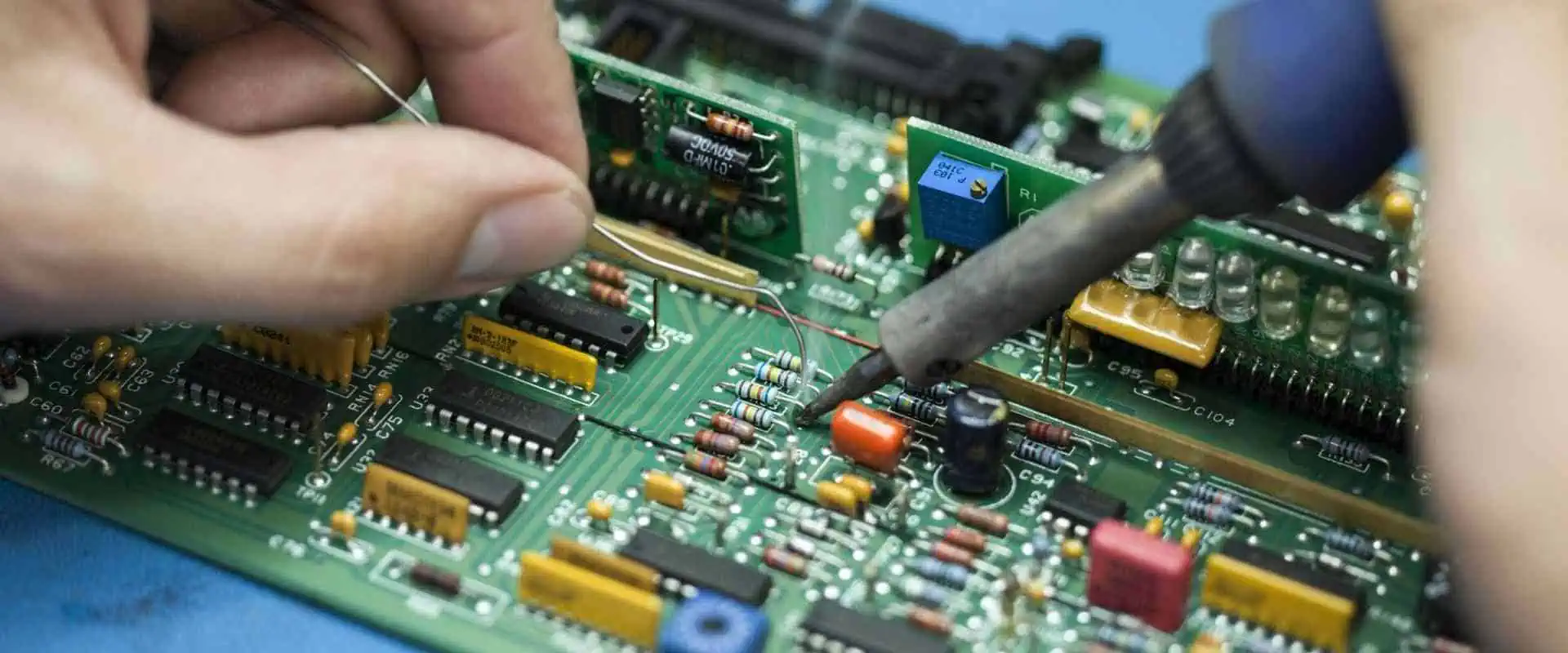
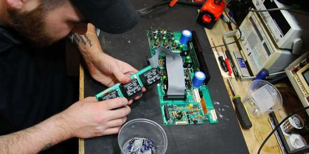
Are you constantly puzzled by your PCBs’ failures, stuck in a frustrating cycle of plating voids, acid traps, and solder bridges? Are you tired of putting your heart and soul into building a masterpiece only to watch it spectacularly crash and burn? Well, worry no more! While repairing PCB failures can be intimidating, it’s easier than you may think with the right tools and knowledge. Repairing a faulty PCB involves standard soldering, component replacement, and reflowing methods. Understanding the risks involved is crucial as taking precautions to avoid damaging the PCB or injuring yourself. So let’s dive into the fascinating world of PCB faults and discover how to troubleshoot them effectively!
PCB Faults
PCB faults refer to issues with a printed circuit board (PCB), such as incorrect component placement, faulty soldering, incorrect circuit design, or physical damage. These errors can result in malfunctions or failures of electronic devices, requiring costly repairs or replacements. Therefore, debugging PCB faults is essential in ensuring electronic products’ quality, reliability, and efficiency and involves identifying and correcting any errors or defects in the PCB design or manufacturing process.
When you solder two pads on a printed circuit board (PCB), an undesirable electrical connection results. This connection is a solder bridge. Excessive solder on nearby pads or the absence of a solder mask layer between the pads can result in this. The electrical connection that results may result in short circuits and other issues. To prevent solder bridges, PCB designers must ensure that solder mask layers are applied correctly, and that solder mask layers are present between adjacent pads.
2. Acid Traps:
Areas on a PCB called “acidic traps” are prone to catching and keeping corrosive leftovers like acid flux. Acid traps are frequent in recessed regions or tight spaces, such as between components. These corrosive residues can harm the PCB and cause corrosion, resulting in electrical shorts and other issues. Therefore, large open spaces between components and solder mask layers should be helpful when designing PCBs to protect recessed areas from acid traps.
3. Plating Voids:
When a hole in a PCB partially has plating material, we can refer to it as a plating void. This can occur when you improperly carry out the plating procedure or when the hole size needs to be more significant for the plating material to fill. In addition, plating voids can bring on electrical shorts, limited current flow, and other issues. Therefore, PCB designers should ensure that they carry out the plating procedure appropriately and that the size of the holes is compatible with the plating substance to prevent plating voids.
4. Environmental Factors:
Environmental factors like humidity and temperature can significantly affect how reliable PCBs are. Components can expand and compress under the influence of high temperatures, resulting in fractures and other mechanical issues. Electrical shorts and component corrosion are both effects of high humidity. PCB designers should build their boards to resist severe temperatures and humidity levels and employ protective coatings to stop corrosion to avoid these issues.
5. PCB age:
PCBs’ performance might deteriorate over time for several reasons. First, components may become more fragile and shatter more easily. Second, electrical shorts can result from connections that become loose. Third, corrosion in plating might lead to electrical issues. To avoid these issues, PCB designers should make their boards as durable as possible and utilize corrosion-resistant coatings.
Soldering problems account for the majority of the printed circuit board flaws. Using the tiny components present on a PCB board makes the technical skill of soldering even more challenging. However, we can reduce soldering faults during design phase and the soldering procedure. The following are some typical soldering flaws:
When your solder fails to connect with a given point of contact properly, often the pad, the open joints, also known as “dry joints,” result. As solder may be present making poor or sporadic contact, the open joints may not always result in a circuit failure. The open joints can result from physical bending or movement, the wrong solder temperature, faulty designing or manufacturing processes, impact during usage or transit, and shifting.
2. The temperature fault:
The printed circuit boards’ operation may degrade due to temperature when stored and attached to components. Parts or joints may break or fail due to extreme temperatures or significant temperature variations. Many assume the highest or lowest safe temperature without considering temperature variations during use or storage. Temperature changes can result in expansion and contraction too quickly, leading to the PCB failing before it should.
3. Plating fault
Electricity travels through holes from one given side to the other of the board. During manufacturing, the engineer plates the hole wall. During this, the operator deposits copper in the endplate part to establish electrical conductivity with reference to the top. An incorrect copper deposition will result in plating voids, which leaves the wall areas without copper coating. We can blame this to tainted materials, air bubbles, contamination occurring in the holes, and other related causes. You can stop this by adhering to the manufacturer’s instructions and clean the equipment appropriately as directed.
4. Electromagnetic Compatibility fault
We link electromagnetic compatibility (EMC) and Electromagnetic interference (EMI) to PCB manufacturing process. While the latter phrase refers to the harmful effects of EMC, the former is typically employed in production and transportation of electromagnetic radiation. These problems may result from design faults, but we can quickly resolve them by reducing the ground surface of the board.
5. Non-wetting fault
The PCB finish dramatically affects the reflow of the solder and the amount of wetting that occurs. With a poor finish and a lot of exposed bare board, the solder reflows with more challenges and poorly adheres to the PCB. In addition, a prolonged storage period makes soldering more challenging and increases the risk of non-wetting. In most cases, solderability and plating thickness have a direct correlation. The plating required for optimum solderability may deteriorate over an extended storage period. Therefore, a PCB in storage for about a year or longer may be more susceptible to non-wetting and poor solderability.
This is the quickest type of examination and most widely applicable method for spotting PCB problems. Therefore, we must visually inspect for any obvious evidence of damage, such as cracks, scratches, or burn marks.
Physical inspections:
You can use a multimeter test the resistance and continuity of various PCB components. It can be helpful to identify any open or short circuits.
X-ray examination:
X-ray inspection is a method for spotting faults that are difficult to see with the unaided eye, like microscopic cracks or hidden solder joints. Using X-rays, the designer can scan the PCB to create an image that is easy to check for defects.
ICT, also known as in-circuit testing, involves inspecting the PCB while it is in use to check for any defects. First, by modeling the PCB’s operation and with specialized testing tools, it looks for any irregularities. Next, put the PCB through its paces during Functional testing: functional testing to ensure that it performs as intended. It is often conducted after completing all other testing and can help identify any performance issues with the board.
Thermal imaging:
This process involves using an infrared camera to identify any hot spots on the PCB. In addition, it might help find any damaged components that are generating an excessive quantity of heat.
When a PCB fault occurs, repairing it can be a challenging process. However, with the right tools, techniques, and knowledge, it is possible to fix many types of PCB faults. Here is a step-by-step procedure for repairing a faulty PCB:
Step 1: Take out the damaged component or pad
Please remove the damaged or defective components or pads to fix a broken PCB. This step may entail carefully removing the element from the board without harming the nearby circuitry using a soldering iron or desoldering tool. In addition, it might be necessary to carefully scrape away the damaged pad with a sharp instrument or blade if it has any damage.
Step 2: Remove the solder and clean the track.
The next step is to clean the track and remove any extra solder or debris after removing the damaged component or pad. Using a soldering iron or desoldering pump, you can carefully heat and remove the solder. Alternatively, gently clean the region around the track using a fine wire brush or abrasive pad.
Step 3: Cover the track with your copper tape.
Next, cover the damaged track or pad with copper tape once you have cleaned the region. You can remedy this by carefully putting a piece of copper tape over the damaged section after cutting it to size and ensuring it extends the track’s whole length.
Step 4: Solder the joints.
The next step involves soldering the joints to firmly attach the copper tape to the board. To achieve this, carefully apply solder to the joint while heating the soldering iron, not overheating the board or harming any nearby components or tracks.
Step 5: Repair the PCB through-hole.
It would be necessary to return the hole in the PCB to its original size and form if you had placed the damaged component through it. To accomplish this, gently remove any extra solder or debris from the hole using a tiny drill bit or reamer, not harming any nearby tracks or components.
Step 6: Insert and solder your component.
Now, please replace the new component and solder it onto the board after you have repaired the hole. To accomplish this, carefully align the element with the repaired hole and solder the leads or pins to the proper board pads.
Step 7: Remove any extra tape from the mended area.
Removing any extra copper tape from the repaired area after soldering the component into place is crucial. To do this, please use a sharp blade or pair of scissors, careful not to harm any nearby parts or railroad tracks.
Cost reductions are one of the critical advantages of debugging PCB mistakes. You may save on pricey rework and recalls by spotting and fixing problems early in the design or production process. The cost of replacing or repairing a malfunctioning unit might be high when you put a product with a faulty circuit board on the market. By debugging PCB defects, you can find these problems before manufacturing and resolve them before they become expensive.
Improve product quality.
Troubleshooting PCB issues might enhance the final product’s overall quality. You can lessen the chance that a product will fail by locating and fixing problems with the PCB design or manufacturing procedure. This strategy can boost client satisfaction and lead to repeat business.
Improved effectiveness
Debugging enables targeted improvements and efficiencies by identifying particular PCB design or manufacturing issues. As a result, you may decrease the time and resources needed to make PCBs by optimizing the design and manufacturing processes, boosting productivity and profitability.
Increased reliability
Identifying and fixing circuit board flaws can enhance the final product’s dependability. A faulty circuit board may cause a product to fail, which could be expensive and harm a company’s reputation. Ensuring the circuit board is error-free increases product dependability, lowers the likelihood of failure, and lengthens product life.
A better understanding of the design
We can better understand the PCB design and manufacturing process through debugging, which helps with design and process optimization. Engineers can pinpoint areas where the design or manufacturing process might be improved by examining issues that arise throughout the debugging phase. This action enables more effective manufacturing techniques and better designs.
Conclusion
It is evident from the above article that PCBs can malfunction in various ways. Several things might cause a defective board, including solder bridges, acid traps, plating gaps, environmental variables, and PCB age. Fortunately, finding and fixing these flaws is possible if you have the necessary equipment and skills. Once you’ve completed all these laborious steps and repaired your damaged PCB, the item should be in working order. With the right equipment, expertise, and understanding, repairing a defective PCB is achievable, even though it may appear difficult. It may take some time and effort, but the sense of accomplishment when the device works again is worth it! With out-of-the-box thinking, anything is possible. Now, let us hope that our PCBs are up to the task!
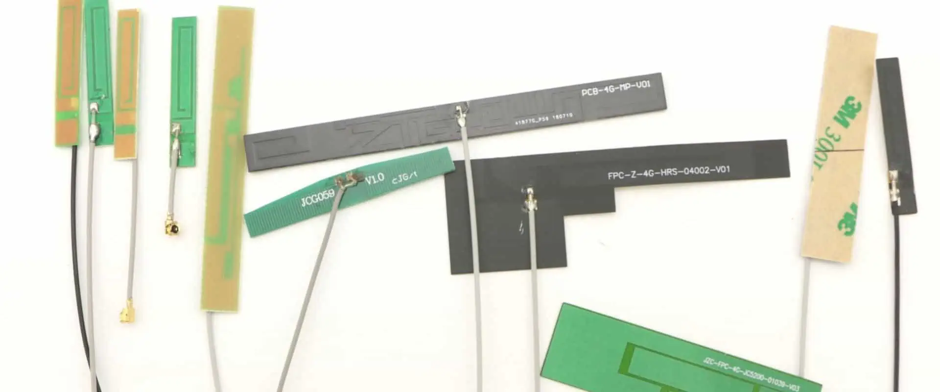
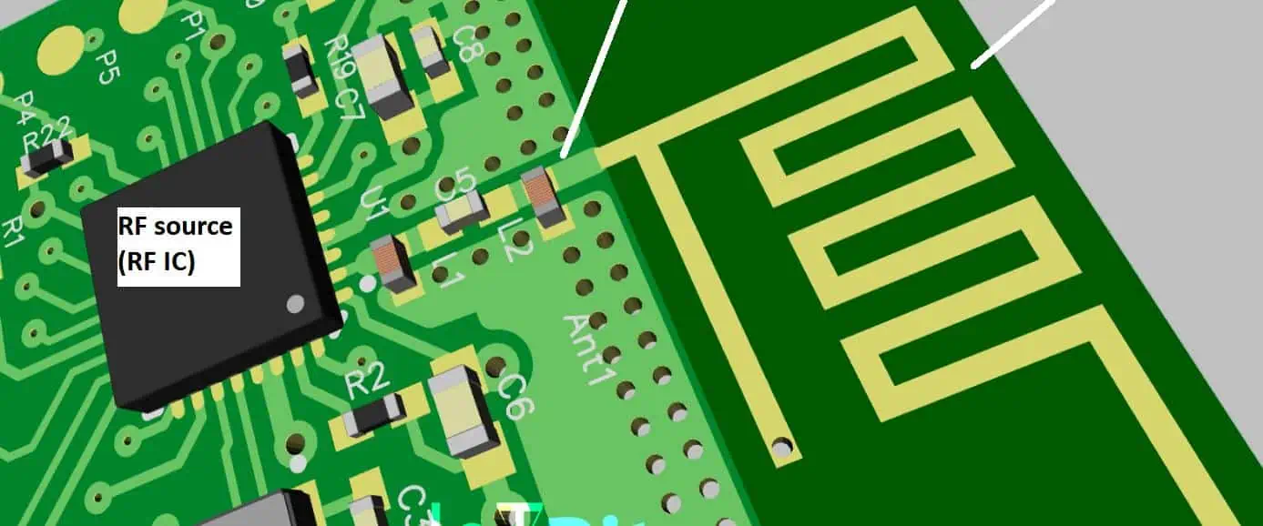
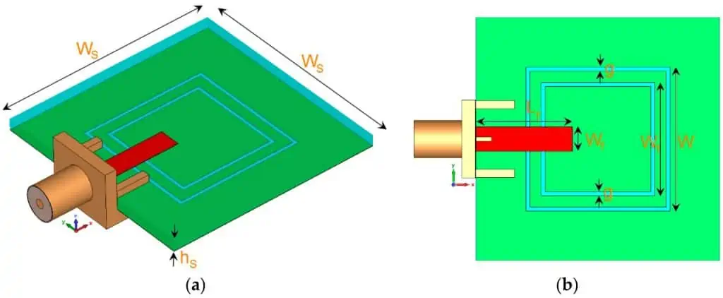
There are different types of antennas. PCB antenna can be printed, thereby, enabling designers to have access to unique architectures and totally custom designs in an assembly. Furthermore, PCB antennas that operate at high frequency allow communication between devices at long distances. These antennas offer several benefits. For instance, they minimize the physical footprint and as well reduce the cost of maintaining a device.
A PCB antenna should be small in size as this helps to improve efficiency. This requires attaching many microstrip patches together. The wavelength of the operating frequency determines the size of the patches.
An antenna used in a PCB is a transducer that transforms current waves in an electromagnetic waves. This antenna is designed to convert current into EM waves in high frequency. A high frequency PCB comprises two antennas. These antennas are attached in the circuit board as an etched copper structure. One of the antennas functions as the transmitted radio frequency signal while the second one functions as the reflected RF signal receiver.
The high-frequency circuit usually produces RF waves and then evaluates the RF wave signals reflected. The base materials of the circuit board transfer the signals to the PCB antenna. Since the PCB antenna is usually compact, it improves efficiency. Also, the antenna combines several microstrip patches to achieve a gain from the compactness of the antenna.
A PCB antenna can be semi-directional, directional, and omnidirectional. An omnidirectional antenna transfer signals in all directions. A semi-directional antenna is for a fixed angle in which the signal propagates. A directional antenna features a single direction in which the signal is required.
To have a good understanding of how a PCB antenna works, it is important to know some details about resonance circuits and impedance matching.
Antennas make up a high frequency PCB and PCB antennas are attached to it. These parts of a circuit board are available in various types. So, what are the types of PCB antennas?
The look of thus antenna is similar to that of a circular or rectangular patch of copper in a circuit. Patch antennas operate at microwave frequencies since short wavelengths can design small-size patches. Portable devices mostly integrate patch antennas since these antennas offer ease of design.
Loop antenna is the simplest PCB antenna. This antenna’s look s similar to a rectangular or round lop. The copper material used in this antenna and the size of the loop determine its efficiency. As regards wavelength, a loop antenna is not ideal for transmission. However, it is widely used as receptors. Since the loop antenna operates in a directional pattern, it helps to locate the transmitter known as radio direction finding (RDF).
It is called slot antenna due to its structure. This antenna comprises a metal plate which has many cuts or slots in it. The electric and magnetic fields in this type of antenna are usually opposite. Slot antenna is widely used in applications such as phased arrays and aircraft radars.
Inverted-F
The inverted-F antenna is widely integrated in the WLAN hardware of our cell phones. As an omnidirectional antenna, the Inverted-F has a large ground plane that helps to ensure maximum efficiency. Copper isn’t used in some part of F patch.
Meander line antenna
A meander line antenna’s conductors are usually folded back and forth. This makes the antenna shorter. Therefore, this helps in achieving a compact size antenna with great efficiency and loss of radiation resistance. Also, this antenna offers decrease in bandwidth.
Since antennas are sensitive to their environment, it is important to consider the layout and design as regards the requirements. Otherwise, this may have a negative effect on the functionality of the wireless device. Minute details such as layer thickness, material, and layer count can impact the performance of an antenna.
Therefore, there are some guidelines that will help you design a PCB antenna successfully. These include:
Antenna positioning
PCB antennas have various operation modes. However, there are some particular positions you need to place them based on the antenna’s radiation level. For instance, you can place them in the corner of the circuit board or along the short side of the board. There are different designs for antennas that are ideal for various positions. Therefore, PCB designers can choose the antenna based on their layout and application.
Closeness to other components
During the design phase of a PCB antenna, you must ensure the embedded antenna isn’t close to other components on the circuits. The height and width of the component determines the distance between other components and the antenna. Components such as LCD s and batteries can have switching speeds. This can help with more signal interference during the functionality of the device.
Keep-out area
Designer need to be sure the components aren’t positioned in the near field around the antenna. Otherwise, this may cause signal interference, which impacts the functioning of the circuit. Furthermore, ensure the area around the antenna isn’t in contact with metallic objects.
Ground planes
The ground plane’s size on a circuit board is a crucial factor you need to consider. This is because wires used for creating communication between different batteries and devices may change if not properly designed. Therefore, designers need to ensure proper sizing of the ground planes. If properly done, batteries and cables linked to the device have less impact on the antenna.
Design the transmission line
In PCB antennas, the transmission line is an RF trace which transmits RF energy. Designers need to design the transmission line at 50Ω as this may reflect signal to the reception. This may result in a degraded signal-to-noise ratio.
Antennas serve two basic functions. These include the emission of electromagnetic waves when there is a current and a voltage. Also, they get electromagnetic waves and transform them into a current and a voltage. The interconnect will have to transfer a signal into the antenna or receive a signal from it.
Furthermore, PCB antennas are usually designed to pick up a magnetic or electric field. Magnetic antennas integrate a loop of wire. The receiver/transmitter element in this system functions in a similar way with a load that completes a circuit board that features the loop antenna.
The physical design of an antenna
A designer aims to define an antenna’s geometry so that they can meet some operating goals such as feedline matching, high radiation efficiency, sufficient bandwidth, directionality, and low loss along front end and feedline. The positioning of an antenna and its physical design will determine these operating properties.
PCB antennas make use of wave resonances present within the structure of the antenna to form a string current oscillation. With this, designers would be able to achieve magnetic and electric field generation around the antenna. Therefore, one of the drawbacks of antenna design is determining the resonances in the structure of the antenna.
After the designer determines the electromagnetic field around the antenna, he determines the radiation efficiency and radiation pattern with software.
The input impedance is another physical aspect to consider for an antenna. You need to know that PCB antennas can posses a reactive component on the input impedance. This will determine how a matching network should be designed for the antenna.
Feedline Design
It is important to design antenna feedlines to get a signal from conductive feedline. This has to be a part of a transmission line designed for a particular impedance that tries to match the impedance of an antenna. Transmission lines are resistive in their characteristic impedance. However, PCB antennas can feature a reactive component.
Therefore, feedline should be designed in a way reduction occurs in the return loss along the feedline. If the feedline isn’t properly implemented, it can limit the bandwidth. Therefore, it is crucial designers choose the right matching method for their exact antenna.
How to Achieve a Better Performance When Designing a PCB Antenna
There are different ways you can improve the performance of your PCB antenna. Below are some ways:
Integrate matching networks when during antenna tuning. This helps in compensating for factors that may impact the performance of the antenna.
Avoid designing an external casing for an antenna as this may interfere with the signal.
Ensure the ground plane you selected is appropriate. If not, this will result in crosstalk between the signals.
Do not place the PCB antenna too close to plastic surfaces. Doing this can have a negative impact on the performance of the antenna. Furthermore, plastic usually features a higher Dk than air. This impacts transmitted signals and can cause losses.
Consider the signal bandwidth when designing a PCB antenna.
Conclusion
Antennas serve two basic functions. These include the emission of electromagnetic waves when there is a current and a voltage. Also, they get electromagnetic waves and transform them into a current and a voltage. Learning how to design PCB antenna requires following certain guidelines to achieve the best result.
In the rapidly evolving world of IoT and embedded systems, the ESP32 microcontroller has emerged as a powerful and versatile platform for developers. This comprehensive guide will take you through the intricacies of ESP32 programming, covering everything from the basics to advanced topics, ensuring you’re well-equipped to tackle any ESP32 project.
What is ESP32?
The ESP32 is a series of low-cost, low-power system on a chip (SoC) microcontrollers with integrated Wi-Fi and dual-mode Bluetooth capabilities. Developed by Espressif Systems, the ESP32 has become a go-to choice for IoT and embedded projects due to its robust features and affordable price point.
Why Learn ESP32 Programming?
Versatility: ESP32 can be used in a wide range of applications, from home automation to industrial IoT.
Cost-effective: ESP32 modules are incredibly affordable, making them accessible for hobbyists and professionals alike.
Rich feature set: With built-in Wi-Fi, Bluetooth, and numerous peripherals, ESP32 is a complete solution for many projects.
Strong community support: A vast ecosystem of libraries, forums, and resources is available for ESP32 developers.
Future-proof skills: As IoT continues to grow, expertise in ESP32 programming will remain valuable.
Overview of ESP32 Family: ESP32-C3, S3, WROOM, CAM Modules
The ESP32 family includes several variants, each tailored for specific use cases:
ESP32-C3: A cost-effective, RISC-V based variant with Wi-Fi and Bluetooth LE support.
ESP32-S3: High-performance variant with AI acceleration capabilities.
ESP32-WROOM: The classic module with a wide range of I/O options.
ESP32-CAM: Integrated camera module for vision-based projects.
Tools You Need for ESP32 Development
To get started with ESP32 programming, you’ll need:
An ESP32 development board
Micro-USB cable
Computer (Windows, macOS, or Linux)
Arduino IDE or ESP-IDF (Espressif IoT Development Framework)
ESP32 add-on for Arduino IDE
Chapter 1: Getting Started with ESP32
ESP32 Features and Specifications
The ESP32 boasts an impressive set of features:
Dual-core or single-core Tensilica LX6 microprocessor
Up to 240 MHz clock frequency
520 KB SRAM
Integrated 2.4 GHz Wi-Fi and Bluetooth
Rich set of peripherals: ADC, DAC, I²C, SPI, UART, etc.
Ultra-low power consumption with multiple power modes
xTaskCreate( Task1, // Function to implement the task "Task1", // Name of the task 10000, // Stack size in words NULL, // Task input parameter 1, // Priority of the task NULL // Task handle );
xTaskCreate( Task2, // Function to implement the task "Task2", // Name of the task 10000, // Stack size in words NULL, // Task input parameter 1, // Priority of the task NULL // Task handle ); }
void loop() { // Empty. Things are done in Tasks. }
Deep Sleep and Low Power Modes
ESP32 offers various sleep modes to conserve power. Here’s how to use deep sleep:
#define uS_TO_S_FACTOR 1000000 // Conversion factor for micro seconds to seconds #define TIME_TO_SLEEP 5 // Time ESP32 will go to sleep (in seconds)
void loop() { if (!client.connected()) { reconnect(); } client.loop();
// Publish a message every 30 seconds static unsigned long lastMsg = 0; if (millis() – lastMsg > 30000) { lastMsg = millis(); client.publish(“esp32/temperature”, “25.5”); } }
### Sending Sensor Data to the Cloud

To send sensor data to a cloud platform like AWS IoT or Google Cloud IoT, you'll need to:

1. Set up a cloud account and create a device
2. Obtain necessary credentials (certificates, keys)
3. Use a library like `MQTT` or platform-specific libraries to connect and send data

Here's a simplified example using AWS IoT:

```cpp
#include <WiFiClientSecure.h>
#include <MQTTClient.h>
#include <ArduinoJson.h>
#include "WiFi.h"
#include "secrets.h"

#define AWS_IOT_PUBLISH_TOPIC   "esp32/pub"
#define AWS_IOT_SUBSCRIBE_TOPIC "esp32/sub"

WiFiClientSecure net = WiFiClientSecure();
MQTTClient client = MQTTClient(256);

void connectAWS()
{
  WiFi.mode(WIFI_STA);
  WiFi.begin(WIFI_SSID, WIFI_PASSWORD);

  Serial.println("Connecting to Wi-Fi");

  while (WiFi.status() != WL_CONNECTED){
    delay(500);
    Serial.print(".");
  }

  // Configure WiFiClientSecure to use the AWS IoT device credentials
  net.setCACert(AWS_CERT_CA);
  net.setCertificate(AWS_CERT_CRT);
  net.setPrivateKey(AWS_CERT_PRIVATE);

  // Connect to the MQTT broker on the AWS endpoint we defined earlier
  client.begin(AWS_IOT_ENDPOINT, 8883, net);

  // Create a message handler
  client.onMessage(messageHandler);

  Serial.print("Connecting to AWS IOT");

  while (!client.connect(THINGNAME)) {
    Serial.print(".");
    delay(100);
  }

  if(!client.connected()){
    Serial.println("AWS IoT Timeout!");
    return;
  }

  // Subscribe to a topic
  client.subscribe(AWS_IOT_SUBSCRIBE_TOPIC);

  Serial.println("AWS IoT Connected!");
}

void publishMessage()
{
  StaticJsonDocument<200> doc;
  doc["time"] = millis();
  doc["sensor_a0"] = analogRead(0);
  char jsonBuffer[512];
  serializeJson(doc, jsonBuffer); // print to client

  client.publish(AWS_IOT_PUBLISH_TOPIC, jsonBuffer);
}

void messageHandler(String &topic, String &payload) {
  Serial.println("incoming: " + topic + " - " + payload);

  // Add your custom message handling here
}

void setup() {
  Serial.begin(115200);
  connectAWS();
}

void loop() {
  publishMessage();
  client.loop();
  delay(1000);
}
Building a Web Server with ESP32
ESP32 can act as a web server, allowing you to create interactive web interfaces for your projects:
Implement continuous integration for ESP32 projects
Customizing Bootloaders and Flash Partitions
Advanced ESP32 development often requires custom bootloaders and partition schemes:
Understand the ESP32 boot process
Create custom partition tables
Implement secure boot for enhanced security
Develop custom bootloaders for specific applications
Conclusion
Summary of Key ESP32 Programming Concepts
GPIO and peripheral management
Wi-Fi and Bluetooth connectivity
Power management and sleep modes
RTOS and multitasking
OTA updates and security considerations
Next Steps: Where to Go From Here
Explore more advanced ESP32 features (e.g., Ethernet, CAN bus)
Contribute to open-source ESP32 projects
Develop commercial products using ESP32
Explore other microcontrollers and compare with ESP32
Resources and Communities for ESP32 Developers
Espressif’s official documentation and forums
ESP32 community on Reddit and Stack Overflow
GitHub repositories with ESP32 projects and libraries
Online courses and tutorials for advanced ESP32 topics
Appendices
A: ESP32 Pinout Diagrams
(Include detailed pinout diagrams for popular ESP32 modules)
B: Glossary of ESP32 Terms
(List and define common ESP32-related terms and acronyms)
C: Useful ESP32 Libraries and Tools
(Provide a curated list of popular libraries and development tools)
D: Troubleshooting FAQ for ESP32 Programming
(Address common issues and their solutions)
This comprehensive guide covers the essentials of ESP32 programming, from basic concepts to advanced topics. By following this guide, readers will gain a solid understanding of ESP32 capabilities and be well-equipped to develop a wide range of projects using this versatile microcontroller.
Electrical impedance plays a crucial role in the way electrical devices function. It is an important and popular concept in physics and electrical engineering. Impedance is the resistance put up by a circuit to an alternating current like an audio signal. In a resistive circuit, impedance and resistance are similar. The electrical impedance formula helps in determining a circuit’s opposition to a current when voltage exists.
Impedance is mostly used when a loudspeaker connects to an audio system. Although the concept of impedance is not fully understood, this concept is widely used in several engineering disciplines. As an important concept in electrical engineering, engineers use the electrical impedance formula to determine a lot of factors in electrical devices. This article describes a combined impact of electrical impedance in an entire circuit.
Electrical impedance measures the opposition of a circuit to a current when there is voltage. It simply describes the opposition offered by a circuit to alternating or direct current. The symbol ‘Z’ denotes electrical impedance. Electrical impedance is usually measured in ohms. Impedance has both phase and magnitude.
The circuit’s frequency determines the opposition of electrical impedance to current. On the other hand, resistance (R) measures how much a substance opposes the passage of electrons among its atoms. Resistance is different from impedance as it contains only magnitude. It can simply be understood as impedance with a phase angle of zero.
Impedance may feature inductive reactance (XL), resistance (R) and capacitive reactance (Xc). Therefore, total impedance is simply the sum of capacitive reactance, resistance, and inductive reactance. Impedance explores the idea of resistance to an alternating current.
The electrical impedance formula is
Z=VI
Where Z is the electrical impedance measured in ohms
I is the electric current usually measured in amperes
V is the voltage measures in volts.
Electrical impedance affects the propagation of signals via a circuit board, the leakage of signals in undesired parts of a circuit board and how power exchanges between components. The effect of resistance and reactance in an AC circuit is usually termed as impedance. The resistance is the opposition of current while reactance opposes electric current flow as a result of frequency dependent elements such as capacitorinductor.
In an AC circuit, the opposition caused by reactance and resistance in the flow of AC is impedance. Therefore, the impedance of an AC circuit in a mathematical perspective is Z=R+- jX. In this case, X is the reactance and R is the resistance.
Before we discuss the difference between impedance and resistance, we need to understand that impedance is related to alternating current while resistance is related to direct current.
Impedance and resistance are two different concepts. While the two concepts can be used in a confusing manner, there are completely different. Impedance measures the extent of opposition of the AC created as a result of capacitance and inductance. Frequency determines the extent of this opposition. Impedance is simply the sum of reactance and resistance.
Resistance, on the other hand, results from the collision of the electrons present in a conductor with the iconic lattice of the conductor. This in turn leads to electrical energy conversion into heat. One could denote that electrical resistance is simply the opposition to electric current. A good resistance changes with frequency.
Impedance is mainly used in alternating current (AC) circuits while resistance is mainly used in direct current (DC) circuits. Also, impedance occurs as a result of resistance and reactance while resistance occurs due to resistive elements.
While impedance has a magnitude and a phase angle, resistance has no phase angle and magnitude. Electric impedance shows energy stored and power dissipation when it is in an electromagnetic field while resistance only reveals power dissipation.
How does Electric Impedance Work?
Electrical impedance is relevant when AC signal is the applied input signal. In a way, electrical impedance shares some properties with resistance. Also, this means the opposition to current flow. However, resistance is independent of frequency. For instance, if you have a simple resistor and you operate DC voltage, the resistance value won’t change in response to frequency.
A circuit’s impedance, on the other hand, changes in response to frequency since it has reactive elements such as the inductor and capacitor. In the case of the capacitor and the inductor, these elements offer a resistance referred to as reactance. The symbol X denotes reactance. Capacitive reactance, also denoted by symbol XC while inductive reactance is represented by the symbol XL.
The inductive reactance will have a value equal to jwL while the capacitance reactance has a value that is equal to 1/jwC. It is important to know that this reactance refers to the ratio between the electric current and the voltage. Therefore, if we consider the ratio of the current and voltage, this will amount to the reactance of the capacitor or inductor.
How to Derive Expressions
From the above explanations, you will realize that the capacitive reactance and inductive reactance are dependent on frequency. This indicates that the value of reactance will change in response to frequency.
Let’s imagine your circuit has the resistive elements, the impedance is the total resistance the circuit provides. The symbol Z represents this impedance. Therefore, the total impedance will be the aggregate sum of the resistive element and also the reactive element. The total impedance will then be equal to R+jWL.
In some cases, it is denoted in the polar form. It indicates that there are some finite phase and finite magnitude. The magnitude of such impedance will be expressed as |Z|=R2 + X2 while the phase of the impedance will be expressed as =tan-1(X/R).
Just like the resistance, the impedance of a circuit is also a ratio of current and voltage. Therefore, if the impedance of any circuit is represented in this way, it indicates the voltage will clearly lead the current and the ratio of the current and voltage signal will provide the value of the impedance’s magnitude.
Electrical impedance is available in two different types. These are the output impedance and input impedance.
Output impedance
For instance, when the circuit gives output voltage when we connect some load at the output terminal. Also, the output voltage must show up across the load’s two terminals. However, from this perspective, it will find some resistance in electric series.
Input impedance
This kind of impedance occurs when you connect some voltage source through the input terminals. When we look at the electric circuit from this opinion, the impedance in this electric circuit is what is known as input impedance. Therefore, input impedance is simply an impedance between the two terminals of an electric circuit.
Applications of Electrical Impedance
Impedance is applicable in different scenarios. This concept even exists in your house. A panel which comprises fuses controls the electricity of your house. Therefore, when there is an electrical surge, the fuses will disrupt the power to prevent or minimize injury. These fuses work in a similar way with a high-capacity resistor. Without these fuses, the electrical system in your house would burn and this will result in paying more cost. However, there is a good solution to this problem. All thanks to resistance and impedance. Impedance has its usefulness in capacitors. Impedance manages electricity flow in a printed circuit board. Without capacitors, your electronics that make use of alternating currents will burn or fry. This is because alternating current (Ac) supplies electricity at an unstable pulse. Therefore, there is a need for a gate to hold back the electricity and allow free flow so the electrical circuits isn’t too loaded or under loaded.
Electrical impedance plays a crucial role in the way electrical devices function. It is an important and popular concept in physics and electrical engineering. Impedance is the resistance put up by a circuit to an alternating current like an audio signal. In a resistive circuit, impedance and resistance are similar. However, in a situation of a reactive circuit that features inductors or capacitors, the frequency of the applied signal determine impedance.
For instance, the circuitry of an audio equipment is designed to make the impedance constant over the whole audio range. It might not be possible to achieve this as loudspeakers change in impedance at or close to the resonant frequency.
Input impedance is a collection of components inside an input jack must receive power from the signal fed in the input. If input impedance evaluates the amount of electrical current a circuit absorbs, the output impedance evaluates the amount of current supplied by an output.
Conclusion
We have discussed electrical impedance, its concepts, formula, and working principles in this article. Also, we looked into the importance and applications of the electrical impedance formula. Electrical impedance affects the propagation of signals via a circuit board, the leakage of signals in undesired parts of a circuit board and how power exchanges between components. The effect of resistance and reactance in an AC circuit is usually termed as impedance.
An attenuator is the first step in the DC voltmeter’s operational process. The attenuator receives the measurement-required DC voltage. Attenuators are used to choose a voltage range. When creating a multi-stage amplifier, either a transistor or a field effect type of transistor is employed.
What Does a Voltmeter Mean?
A voltage meter, also referred to as a voltage meter, can be described as a device that gauges the potential difference or voltage existing between the two points present in the electrical or electronic circuit. DC – Direct Current or AC – Alternating Current circuits are typically the two types of circuits that the voltmeter is used for. Nevertheless, specialist voltmeters may also be employed to measure RF or Radio Frequency voltage.
Typically calibrated in millivolts, kilovolts, or volts, a voltmeter aids in measuring voltages.
A voltmeter can be connected in a parallel form to your device to measure the voltage. This configuration is crucial because parallel objects frequently encounter the same or similar potential difference. For the most part, it shares the same drop in voltage with the circuits, which is why it is linked in parallel.
A voltmeter’s internal resistance is also quite high. The reason for this is just to gauge the probable difference between both the circuit’s two points. As a result, this measuring device’s current stays constant. Explaining further, the voltmeter’s high resistance will make it difficult for current to pass through it. That enables the instrument to measure voltage accurately.
By moving a pointer against by the fully calibrated scale, a DC voltage meter can be described as a gadget that measures whatever DC voltage is applied onto it. The PMMC meter offers a calibrated scale. Be aware that the voltmeter is another name for voltage meter.
You should also be aware that this voltage being monitored passes first through an attenuator then a DC gain amplifier. The DC voltage is input into an attenuator before being routed through DC linked amplifiers to be monitored by a DC voltage meter.
You can question the purpose of first attenuating a signal then boosting it. In order to choose a specific range, the solution towards this question involves the fact that an attenuator can be used. In order to conveniently get voltage readings, it is also necessary to amplify the signal to the point where it is of a magnitude strong enough to divert the PMMC meter’s pointer.
The DC voltage meter can be made by joining a very large resistor in a parallel form with a circuit we would like to determine the voltage in with this instrument in series.
The deflecting torque is produced by this interaction between both fields created by the fixed coils and moving coils. This instrument sees little use since it’s only employed in DC measuring circuits.
DC Voltage Meter Types
The Direct-Coupled Cascaded Amplifier DC Voltage meter and the Chopper Type DC Voltage meter are the two different types of the DC voltage meters. There are two possible designs for the first type of DC voltage meter. The first is to use bipolar junction transistors. Using field effect transistors is the second.
Direct-coupled cascaded amplifier Using BJT
The attenuator in this uses a variety of resistors with appropriate values. NPN and PNP transistors are both employed here, and they are both directly cascaded in order to ensure that there is a reduction in the use of more components. The lesser the components utilized in circuits, the lesser the complexity.
DC Voltage Meter Utilizing BJT
Everyone is aware that a transistor has always been referred to as a current-controlled device when used with the BJT. As a result, resistors must always be connected in series with any device that uses current to alter or control it. As a result, the transistor of Q1 is linked in series with the resistance having about 14M.
This attenuator network would assist in choosing a specific voltage range. Also, a high output amplifier is created by a network of some transistors linked to one another. When the cascaded amplifier’s amplified voltage enters its PMMC meter, this same pointer there begins to deflect on the calibrated scale. We can use this method to gauge the voltage provided to it.
Cascaded Direct Coupled Amplifier FET-based DC Voltage Meter
Low sensitivity is produced by the BJT-based direct coupled amplifiers, which also places a heavy load on the input circuits. Because of this, the idea of the direct coupled amplifiers using FET was developed. The FET’s high impedance is by far its greatest benefit.
The input circuits connected into the DC voltmeters does not become loaded because of a high input FET impedance. This leads to a substantially higher sensitivity afforded by such a circuit compared to the prior one.
The connecting design of the DC voltmeter employing a FET and a BJT are identical. The fact that this FET is now a voltage-controlled device is the only distinction. This resistance network attached to a voltage-controlled device is therefore always in shunts.
DC Voltage Chopper Type Meter
The shortcomings of the Direct-Coupled Amplifier DC Voltage meter were addressed by the development of the Chopper DC Voltage Meter. The issue of drift was significant. By employing modulators and capacitors, the drift issue in DC voltmeters of the chopper type can be solved.
The Chopper DC voltmeter’s circuit gives us a quick overview of how it operates. A chopper modulator transforms a DC voltage that needs to be measured into an AC signal. An AC amplifier then receives the AC signal. The drift problem is resolved by the capacitors employed prior to and following the amplifier circuits. With a chopper demodulator, an AC signal is transformed into a DC signal and then sent through a low pass filter ensuring the elimination of AC ripples where present.
AC Voltage Meter vs DC Voltage Meter: What’s the Difference?
The main distinction between an AC and a DC voltage meter is that the latter measures the DC voltage’s peak value while the latter measures its RMS value. The operating principle of each type of voltmeter—DC and AC—distinguishes them from one another significantly. This DC voltmeter chooses a specific voltage, mitigates the remainder of the voltage range, amplifies the chosen voltage, and then transmits it into the PMMC meter.
Before amplifying a signal, an AC voltmeter utilizes the rectifier to convert the AC signal into DC. The DC is then sent to a moving coil magnetic meter to change the pointer’s indication and measure the AC voltage’s RMS value.
The permanent moving coil meters, multistage DC amplifiers, and attenuators are all parts of DC voltmeters. The DC voltage’s peak value applied to your DC voltmeter is measured.
The attenuator, multistage amplifier, rectifier, and PMMC meter are all components of a AC voltage that should be measured. AC voltmeter circuits receive the measured voltage as input. Rectifiers are used to transform AC electricity into DC voltage.
Key Variations Between the AC and the DC Voltage Meter
The main distinction between an AC and DC voltage meter is the measurement quantity. As opposed to measuring AC voltage, this DC voltage meter helps in measuring DC voltage.
The fact that the DC voltage meter doesn’t utilize a rectifier before a multistage amplifier is another significant distinction between a DC voltmeter and an AC voltmeter. AC voltmeter on the other hand makes use of a rectifier before a multistage amplifier.
The AC voltage’s RMS value is measured by an AC voltmeter, whereas the DC voltage’s peak value is measured by a DC voltmeter.
You will eventually need to utilize a Voltmeter for measuring the different voltage levels when analyzing the electronic and electrical circuits operation or attempting to comprehend why the circuit fails to function as planned. Voltmeters are devices used for measuring voltage. They can be digital or analogue, or they can be a standalone device or a part of the digital multimeter, which is now more widely used.
Voltmeters may be employed to measure sinusoidal AC voltage as well as DC voltage, however adding one as a tool for measurement into the circuit may disrupt its operation in a steady state.
A “Voltmeter” can be described as the device that, because its name suggests, measures voltage (V), or potential difference that exists between any two locations in a circuit. The voltmeter should be attached in a parallel form with a component which voltage you want to measure in order to measure voltage.
A drop in voltage across one supply or component can be measured using a voltmeter, as well as the total voltage drop across multiple places or components inside the circuit.
Conclusion
An important component of the instrumentation of electronics is a DC voltage meter. This exact application we are dealing with determines whether to utilize an AC voltmeter or DC voltmeter. You should make use of the DC voltage meter when handling DC circuits.