What is Custom 3D Printing?

Custom 3D printing

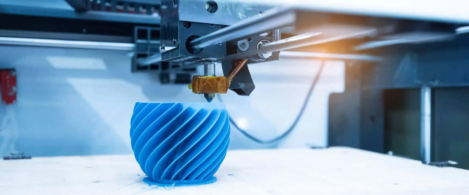
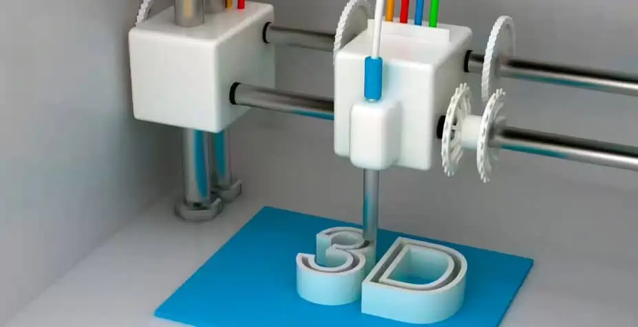
Digital files are useful for creating solid objects of three dimensions via additive manufacturing, also known as 3D printing.

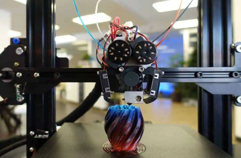
Using additive methods, 3D printed objects are produced. In the additive process, the object is made by adding material layers one after another until the product is made. It is possible to think of every layer as the object’s thinly and finely sliced cross-section.

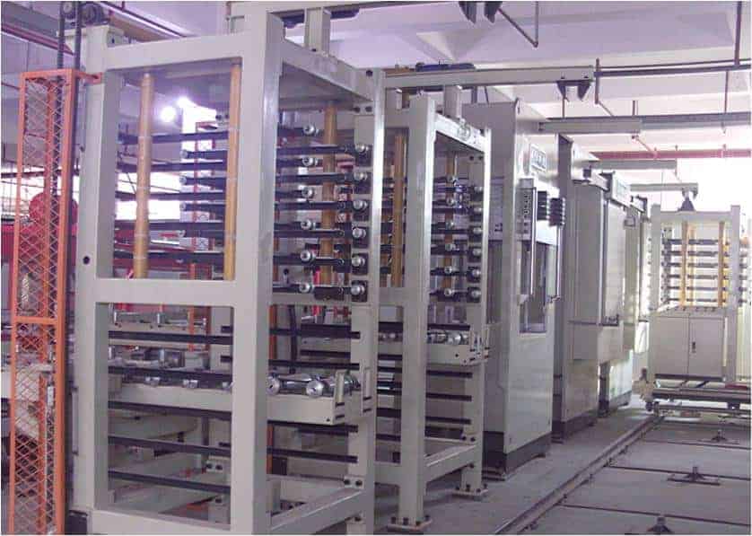
Subtractive manufacturing, that involves hollowing a plastic or metal piece out using the milling machine, is the reverse of 3D printing. With 3D printing, you can create intricate shapes with less material compared to conventional production techniques.

How Do 3D Printers Operate?

Custom 3D
Custom 3D

The 3D model is where it all begins. You may choose to make one right from the start up, or just get it downloaded from the 3D library

The 3D Software

Software instruments come in a wide variety ranging from open source to commercial quality.

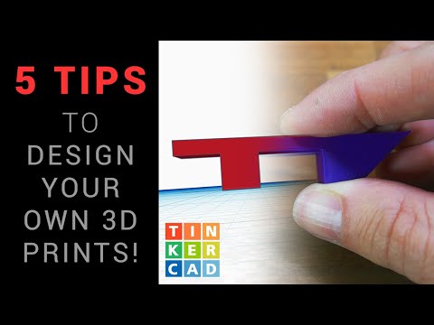
We frequently advise new users to start using Tinkercad. You don’t need to install Tinkercad on your pc because it operates in the browser for free. Tinkercad provides tutorials for beginners and includes a tool to export the model in form of printable file, such as .OBJ or .STL

The following step involves getting the printable file ready for the 3D printer. We refer to this as slicing. From the printable file into the 3D printer through slicing. Slicing is the process of using software to divide the 3D model to thousands or hundreds of layers.

When the file has been divided, it is prepared for the 3D printer. You can use USB, Wi-Fi, or SD to send the file into your printer. The sliced file has become prepared for layer-by-layer 3D printing.

YouTube video

The Benefits of Custom 3D printing

The advantages of layer-by-layer construction of parts allow for design possibilities which were previously not possible using conventional techniques like machining, injection molding, or casting.

  • Geometries that are intricate and organic with little effect on part price
  • creation of a single item from a multi-component assembly
  • no initial tooling expenses
  • Rapid part manufacture within 24 hours or a day
  • Internal features with cutting-edge applications involving flow applications and heat transfer.

Industry for Custom 3D Printing

FULL PCB MANUFACTURING Quote

The industry for 3D printing has achieved critical mass, and those who haven’t included additive manufacturing in the supply chain yet are now a part of a minority that is constantly getting smaller.

Once solely useful for prototype as well as one-off manufacturing, the 3D printing is now quickly evolving into a manufacturing technology.

The majority of the existing 3D printing market is driven by the industrial sector. By 2026, the overall market for 3D printing is expected to grow to $41 billion, according to Acumen Research.

As it develops, the technology for custom 3D printing has the potential to drastically alter virtually every major business as well as the way future generations will live, play, and work.

Examples of the Custom 3D printing

As 3D printing is utilized in practically every industry you can imagine, it spans a wide range of materials and technologies. It’s crucial to think of it as the collection of many industries having a wide range of potential applications.

Some examples are highlighted below:

  • dental products
  • consumer products like furniture, design, footwear, and eyewear
  • prosthetics
  • Industrial products like prototypes, manufacturing tools, etc.
  • reconstructing fossils
  • architectural scale maquettes & models
  • movie props
  • reconstructing evidences in the forensic pathology
  • replicating the ancient artefacts

Rapid Manufacturing & Rapid Prototyping

3D Printing
3D Printing

Ever since late 1970s, businesses have utilized 3D printers to make prototypes as part of the design process. Rapid prototyping is the process of using the 3D printers to suit these needs.

The benefits of using 3D printers in rapid prototyping

Inside a nutshell, it’s quick and reasonably priced. It takes days rather than weeks to go from having an idea to having a 3D model inside your hands and finally a prototype. Making iterations is simpler and less expensive, and you do not even require pricey molds or equipment.

Rapid manufacturing is another application for 3D printing in addition to rapid prototyping. Using 3D printers to serve small batch or short run custom manufacturing, rapid manufacturing can be described as a new manufacturing method.

Applications of Custom 3D Printing

Automotive

3D printing has been used by automakers for a very long time. Automobile manufacturers print end-use components as well as spare parts, jigs, tools, and fixtures. On-demand manufacturing made possible by custom 3D printing have reduced inventory levels and accelerated manufacturing and design cycles.

Globally, auto enthusiasts are adopting parts that are 3D printed to restore vintage vehicles. One such instance involves the use of 3D-printed components by Australian engineers to revive the Delage Type-C. They would just have to print components that had been out of manufacturing for many years in order to do this.

Aviation

Aviation is a big fan of additive manufacturing, in large part because of the potential of stronger, lighter structures that 3D printing offers. Recently, the aviation industry has experienced a ton of advances, including the emergence of printed versions of more vital components.

Construction

A building could be printed, but how? It is, indeed. Commercially available 3D printed homes are already available. Several businesses fabricate pieces in advance, while others manufacture it on-site. On our website, the majority of the tales on concrete printing are about large-scale systems that use rather large nozzles to produce a lot of concrete at once.

It works well for consistently laying down the concrete layers quickly. Yet for incredibly delicate concrete work which fully utilizes 3D printing’s capabilities, something a bit more nimble with a beautiful touch is required.

Consumer products

When we initially began blogging regarding 3D printing, it wasn’t yet prepared to be employed as a large-scale production method. There are many instances of 3D-printed consumer goods in use today.

Footwear

The Adidas’ 4D line features a midsole that is entirely 3D printed and is made in enormous quantities. Back then, there was a piece describing how Adidas intended to sell a hundred thousand pairs of AM-infused sneakers by 2018 despite originally releasing only 5,000 pairs for public use.

Eyewear

By 2028, it is expected that the market for 3D printed eyeglasses would be worth $3.4 billion. The category of the end-use frames is one that is rapidly expanding. The fabrication of eyewear frames is a good fit for 3D printing since the specifications of the individual can be processed easily.

Jewelry

The 3D printer may make jewelry in two different ways. E ither indirect or direct production procedure might be applied. Direct manufacturing is the manufacture of the object directly from a 3D design, whereas indirect manufacturing refers to the use of a 3D-printed object (pattern) to eventually produce an investment casting mold.

Healthcare

Recent headlines frequently mention implants made via 3D printing. These situations are frequently experimental, that can give the impression that custom 3D printing continues to be an emerging technology in healthcare and other medical fields, but that is no longer the case. Over a hundred thousand hip replacements were 3D printed with GE Additive over the past ten years.

A hearing aid is another medical device that was successfully 3D printed and manages to blend in. It is easy to understand why additive manufacturing is used in the production of 99% of all hearing aids.

Education

3D printers have been used in classrooms by teachers and students for a while. Students can quickly and affordably actualize their ideas thanks to custom 3D printing.

Universities have historically used 3D printers for various disciplines, despite the fact that degrees focused on additive manufacturing are still relatively new. One can participate in a variety of educational programs related to 3D printing. Universities provide classes in subjects related to 3D printing, such as 3D and CAD design, which may eventually be used in custom 3D printing.

Frequently Asked Questions

What is the price of 3D printing?

The design, material, technique, as well as post print procedures all have an impact on the cost for every part of custom 3D printing. The majority of a part’s cost is typically accounted for by post-print processes, particularly when manual work is required.

If cost seems to be a major consideration, laser powder sintering methods like MJF and SLS are typically the most advantageous economic solutions for the end use components.

Determine important design needs including temperature resistance, strength, water resistance, durability, or aesthetics before choosing a custom 3D printing process. This will frequently enable you to decide if a plastic or metal 3D printer is required for your applications.

What benefits does Custom 3D printing offer?

Speed is included among 3D printing’s main benefits. Design flexibility, cost savings, including tooling without tooling investment are other benefits.

What is the purpose of 3D printing?

Historically, manufacturers have used 3D printing as a fast prototype technique. Custom 3D printing can be frequently used for the creation of finished parts due to improvements in post-processing choices and additive materials suitable for engineering applications.

Conclusion

Custom 3D printing is utilized in practically every industry you can imagine; it spans a wide range of materials and technologies. It’s crucial to think of it as the collection of many industries having a wide range of potential applications.

What are the Duties and Responsibilities of the Computer Hardware Engineer?

Embedded Hardware Engineer

The computer hardware engineer takes charge of creating and designing electronic items like circuit boards, processors, modems, computer chips, printers, keyboards, storage and memory units, data switches, as well as other electrical and mechanical system components. They can seek employment in many different sectors, including Technology, manufacturing, and R&D.

The computer hardware engineer may work alone or with other IT specialists as a team member. The computer hardware engineer may also be in charge of upkeep and technical assistance for internal hardware users in some businesses.

The majority of businesses now need the computer hardware engineer to assist them flourish due to the growing push toward digitalization.

By 2028, there will be a 6% increase in computer hardware engineer demand, predicts the U.S. BLS. Read on if you wish to participate in this trend.

YouTube video

What Services Does the Computer Hardware Engineer Render?

Among the duties entrusted to the computer hardware engineer are:

  • Creating innovative computer hardware designs and the schematics needed to construct components like circuit boards and microchips.
  • Before it is actually released, this same computer hardware designed is tested.
  • The test results are analyzed, and design changes are made as needed.
  • Updated computer features are made to guarantee that they’re still compatible with new software.
  • Computer hardware manufacturing is overseen.
  • Computer designs and components are worked on.

A large number of hardware engineers create components utilized in manufactured goods that include processors as well as other components of the computer, which connects to internet.

For instance, many modern automobiles, home appliances, as well as medical equipment come equipped with Internet-capable computer systems.

The computer hardware experts make ensuring that the newest software and computer hardware are compatible. As a result, software developers and hardware engineers frequently collaborate. For instance, the software and the hardware for smartphones as well as other devices are routinely created concurrently.

What qualifications and skills must a computer hardware engineer possess?

FULL PCB MANUFACTURING Quote

Education  

A BSc. in computer engineering is required for a position as computer hardware engineer. Nonetheless, some organizations also take into account applicants with degrees in electrical engineering or computer science.

The computer hardware engineer should be conversant with programming since this individual will need to tamper with a computer software.

Obtaining a master’s degree can be beneficial for those looking to land managerial employment. An Engineer can search for schools with accreditation.  Also, obtaining certificates might help you develop in your work and earn more money.

Skills

Analytical skills are necessary for a computer hardware engineer to evaluate complex equipment as well as troubleshoot problems. To create designs that would operate with a new software, they ought to be imaginative. They also need to be effective communicators because they collaborate with others on a regular basis.

Additional Skills

The computer hardware engineer need to be able to put in lengthy shifts, especially if they have urgent and backlog jobs to complete.

Key Qualities that a Computer Hardware Engineer Must Have

Analytical skills: The computer hardware engineer study digital circuits within hardware to get the optimal design using tools for computer programming.

Critical-thinking skills: Engineers with critical thinking abilities may define objectives, question presumptions, and assess the advantages and disadvantages of potential solutions and answers.

Problem-solving skills: The computer hardware engineer has the ability to analyze complicated issues related to computer hardware, come up with potential solutions, test them, as well as decide how to execute them most effectively.

Communication skills: The computer hardware engineer frequently works in teams and need to interact with other engineers, programmers, and software developers, in addition to non-technical team members.

How to Be a Computer Hardware Engineer

How to select a PCB manufacturing and PCB assembly manufacturer as an electronic engineer

The computer engineer typically starts their career by obtaining a bachelors of science degree in the field.

Computer science and electrical engineering studies are both necessary to become a computer engineer.  A degree in the electrical engineering as well as computer science field is, nonetheless, acceptable to some employers. To become a good computer engineer, you must have understanding in both fields. Some students of engineering take part in internship programs while pursuing their degrees so that they will graduate with work experience.

Others, however, might want to pursue an associate’s degree in engineering or computer science. A two-year associate’s degree enables you to start working sooner. As a result, you can keep working as technicians or assistants while pursuing your Bachelor of Science degree. As you work toward your dream of becoming the computer engineer, you acquire practical experience and earn money.

Math, computer science, and science coursework are typically covered in computer engineering curricula.

Considering that computer engineering includes both software and hardware components, the training you take may also cover software, computer programming, circuit boards, or hardware, depending on the specialty you choose. Moreover, good communication abilities, analytical abilities, critical thinking, and problem-solving abilities are essential. Being a computer engineer requires you to always be developing, reviewing, and collaborating with others.

Level of Education

Although being the minimum requirement, a Bachelor of Science degree only opens the door to entry-level jobs. A master’s or doctoral degree is often preferred by employers. In addition, it is expected that you’ll remain learning all through your career to stay up with the constant advancements in technology. Also, you should make sure the program has been reviewed by ABET before applying for degrees.

To guarantee that requirements are met across the board, the organization approves computer engineering programs. Student performance, program curriculum, instructor credentials, facilities, as well as student resources are among the characteristics that they consider. Each program’s quality and worth are demonstrated by its ABET accreditation. We recommend visiting their website.

Career Prospects for the Computer Hardware Engineer

RF Hardware Engineer

Within the following 10 years, hiring of the computer hardware engineer is predicted to increase by 5%, roughly as quickly as that of the average that suits all occupations.

Within ten years, there are expected to be, on average, 5,300 opportunities for the computer hardware engineer, notwithstanding the modest expansion in employment. The majority of all those openings have been anticipated to be caused by a desire to replace employees who switch to other occupations or leave the labor force, like retiring.

Employment of the Computer Hardware Engineer

As more sectors other than the electronic and computer product manufacturing sector start to investigate and create their unique electronic devices, there will likely be an increase in need for such engineers. Yet, since these worksites encompass broad networks and geographical areas, centralized networking and computing services may result in a reduction in the requirement for engineers.

These professionals may see some employment as a consequence of a rise in the hardware startup companies and the continuing growth of the devices with different computer chips built in, like home appliances, medical equipment, and autos.

What Careers are Related to the Computer Hardware Engineer?

Aerospace engineers

Spacecraft, aircraft, missiles, and satellites are the main objects that aerospace engineers usually design. They also develop and test the prototypes to ensure they work with respect to the design.

Information and Computer Research Scientists

Information and computer research scientists create novel computer methods and develop creative applications for already existing technologies. They research and resolve challenging issues in computing across business, science, health, and other disciplines.

Information and Computer Systems Managers

The planning, coordinating, and direction of computer-related operations inside an organization is the responsibility of information and computer systems managers, also known as information technology managers also known as the IT project manager. They are in charge of putting in place computer systems to accomplish an organization’s information technology objectives.

Computer Network Architect

LANs, WANs, as well as intranets are all designed and built by the computer network architect. Slight connections across two offices and next-generation networking abilities like cloud infrastructure which serves multiple clients, are both included in these networks.

Computer Programmers

Coding is created and tested by computer programmers to ensure that software and computer applications run efficiently. They convert the blueprints for programs developed by engineers and software developers into commands that the computer can understand.

Electronics and electrical engineers

Electric motors, communications systems, navigation and radar systems, and equipment used in power generation are just a few examples of the electrical equipment that the electrical engineer designs, develops, tests, and oversee the production of. Electronics engineers create and design a variety of electronic gadgets, like portable audio players, GPS devices, as well as communications and broadcast systems.

Mechanical Engineers

Tools, engines, as well as other thermal and mechanical devices and sensors are designed, developed, constructed, and tested by mechanical engineers.

Computer Systems and Network Administrators

Virtually every organization relies on computer networks. Computer and network systems administrators handle the daily operations of the network.

Software Developers

The innovative minds driving computer programs are software developers. Some people create the software that enables users to perform particular tasks on computers or other devices. Others create the operating systems that power the gadgets or regulate networks.

Conclusion

To ensure that computer components function with latest and most recent software, the computer hardware engineer needs to be passionate about and interested in working with computer components.

Functions of Basic Electrical Components in Electronic Circuits

PCB Embedded Components

Electrical components are crucial in electronic devices. They are responsible for the functioning of any electronic device. These components are often installed on a bare circuit board. A circuit board that features electronic components is an assembled circuit board. Electrical components are designed for use in electronics and electrical projects.

There are many basic electrical components available in the circuits of most peripherals. These components are the foundation of electrical and electronic circuits. Electrical circuits available in different devices share some similarities. Since there are numerous electrical components, it is necessary to really comprehend the functions and attributes of all the components.

What are Electrical Components?

Electrical components help a circuit to function. These components produce, convert, and transmit electrical energy. Examples of electrical components include resistors, diodes, transistors, and inductors. These components enable an electrical circuit to work. They are available in various shapes and sizes. Electrical components control the flow of electrons in an electrical circuit.

Electrical components feature at least two terminals which connect to the circuit. The complexity of a circuit determines the number of electrical components present in it. These components are in two different categories. These are active components and passive components. ย 

YouTube video

Active components

Active components use electrical signals to produce electric power. These components carry out their functions since they get their power through an electricity source. Also, these components need some source of energy that is gotten from a DC circuit. Active components have directionality or gain. Examples of active components include transistors, oscillator, and IC.

Passive components

Passive components can save or maintain energy in a voltage or current form. Also, these components donโ€™t depend on a power source. Therefore, they donโ€™t have the capability to amplify. They donโ€™t have any directionality or gain. Examples of passive components include inductors, capacitors, resistors, and transformers.

Basic Electrical Components in a Circuit

FULL PCB MANUFACTURING Quote

Transformer

A transformer is an electrical component that changes the levels of current and voltage in a circuit. This component has 2 coils of wire which are linked by an iron core. The transformer integrates mutual induction to transform electric energy from a circuit to another. Also, this component helps in decreasing or increasing AC voltages.

A transformer works based on the Faradayโ€™s laws of electromagnetic induction. This law talks about the mutual inductance between two circuits connected by a magnetic flux. Transformers enable the conversion of power form a circuit to another with a different level of voltage. These basic electrical components are available in a range of sizes.

Resistor

This electrical component helps to control or limit electrical current flow in a circuit. Also, it offers a particular voltage to a transistor. A resistor absorbs energy when electrical current flows through it. The energy absorbed by the resistor is usually discharged in the form of heat. This component functions based on Ohmโ€™s law. According to Ohmโ€™s law, voltage applied across a resistorโ€™s terminal has a direct proportion to the electrical current that flows via it.

Resistors have variable or fixed resistances. Resistor functions when there is a need to control current flow at a desired level.  A resistor with a fixed resistance sets the appropriate conditions in a circuit. The resistance of a fixed resistor is usually determined during the design process of a circuit. In a variable resistor, there is a change in resistance based on the requirements of the electronic circuits.

Integrated Circuit (IC)

An IC is one of the most basic electrical components in a circuit. Also known as a microchip, this component has millions of transistors, capacitors, and resistors. An integrated circuit can act as a microprocessor, oscillator, and timer. This component is the foundation of several devices like computers, cell phones, and more.

An integrated circuit is widely integrated in computing devices. It can be nonlinear or linear based on its application. A linear IC has a continuous variable output. However, the level of input signal determines the output. Furthermore, linear ICs function as radio frequency and audio frequency amplifiers. A non-linear IC otherwise known as digital circuit functions at specified states. This IC is commonly used in computer networks, modems, frequency counters, and more. The logic gates are the foundation of a non-linear IC.

Transistor

This semiconductor device has three terminals. It usually functions as an amplifier or a switching device. A transistor can build complex electrical systems. It comes in two major types which includes NPN and PNP. The NPN transistor is widely integrated in most circuits. The three terminals of a transistor include the collector, base, and emitter. The base of the transistor activates it while the emitter functions as the negative lead. The collector is the positive lead.

You can see a transistor as a switch that features several output states. Also, it is impossible to change these output states manually. To change the switch between different states, there is a need to run current via the transistor. You can regulate the current that passes through the transistor to regulate the output state. The main functions of a transistor include amplification, switching, and controlling electrical energy.

Battery

Active Components VS Passive Components

Battery is an electrical component that functions as a source of electric power. This component uses electrochemical cells to provide electric power. Each cell in the battery comprises an electrolyte, cathode (+), and anode (-). Batteries functions based on the electrochemical reaction principle. These components are containers that save potential and electrical energy.

Batteries convert chemical energy to electrical energy in order to provide power to several electronic devices. These components are available in  different sizes and types. There are secondary batteries and primary batteries. Primary batteries discharge their power completely before they are thrashed out. However, secondary batteries can still be used after they have discharged their power.

Inductor

This two-terminal electrical component saves electrical energy in form of magnetic energy. Inductor comprises a conductor which winds in a coil. This electrical component functions according to the Inductance law by Faraday. According to this law, a current passes into its coil and from its left to right. In this case, the coil produces a magnetic field.

An inductor resists changes in a current. Inductance can be described as an inductorโ€™s ability to generate magnetic lines. The inductance of an inductor is calculated by using this formula L= (ยต.K.N2.S)/I

Where

L represents inductance

ยต represents magnetic permeability

K represents magnetic coefficient

S represents cross-section part of the coil

N represents the number of turns of the coils

Circuit breaker

Circuit breakers can be described as electrical components that prevent an electrical circuit from damaging. Overload or short circuit can cause damages to an electrical circuit. With a circuit breaker, such damages can be prevented. The main function of this electrical component is to disrupt the flow of current and detect any fault.

A circuit breaker comprises two contacts like fixed and moving contact. The fixed contact has a spring which keeps the moving contact firm after closing while the moving contact integrates stored energies to make and break the circuit. Furthermore, a circuit breaker has two different coils which are tripping and closing coil. The tripping coil trips the circuit while the closing coil closes the circuit.

Diode

This is another basic electrical component that blocks current that goes against the flow in a wire. A diode enables current to pass through one direction. This component which is made of a semiconductor material feature two different terminals which are cathode and anode. Diodes are commonly used to convert Alternating current to direct current.

These basic electrical components are made of a vacuum tube or a semiconductor material. Therefore, diodes are in two types. These are semiconductor diodes and vacuum diodes. Vacuum diodes have two electrodes which are inside a vacuum glass tube.

Fuse

A fuse shares some similarities with a circuit breaker. It helps a circuit breaker to protect the electric circuit from overload. A fuse heats up and gets damaged when there is power overload. When there is an extreme current, the wire in the fuse heats up and melt. This stops the flow of current.

A fuse is available in various types. Each of this fuse is designed to sustain various amounts of currents. Therefore, a fuse features various ratings like 13A, 3A, and 5A. For example a fuse with a rating if 13A will melt at 13A. A standard fuse comprises connection, metal-fuse elements, contacts, and support body. This electrical component functions according to heating effect principle.

Motor

A motor transforms electrical energy into mechanical energy. Motors are available in appliances around us. You will find them in common appliances and even the most complex computers. These basic electrical components comprise bearings, conduit box, rotor, stator, eyebolt, and enclosure. Motors are available in different types. This includes stepper motor, AC inductance motors, and switched reluctance motor among others. Motors perform better compared to pneumatic and hydraulic alternatives.

Relay

A relay is an electromechanical switch that uses low power signal or one signal to regulate the circuits. In the past, relays function as amplifiers. However, these electrical components evolved to offer more functions in the technology sector. The basic components of relays include electrical contacts, an armature, an electromagnet, and a spring. Relays carry out logical operations on telephone exchanges and computers.

Relays integrate low currents. However, relays can also control high electric currents. Relays can either me solid state or electromechanical. They can detect irregularities that occur during power distribution.

Switch

A switch is an electrical component that breaks a current, disrupt a current and provide current from a conductor to another. This electrical component uses the on and off mechanism that performs this task. Switch are classified in four main types which are single pole sing throw, double pole single throws, double pole double throws, as well as the single pole double throws.

LED

LED which means light emitting diode is a semiconductor device that emits light anytime there is a flow of current. This device is available on almost all appliances. You will find it on TV remote controls, hard disks, keyboards, and more. They function as status indicators in computers. This means that they help to indicate the state of current in a circuit. This light-based indicator makes it easy to check the output current or voltage.

Applications of Electrical Components

active and passive components

An electronic circuit comprises different electrical components like inductors, resistors, diodes, ICs, and more. Electrical components are integrated in various devices. Below are examples of where electrical components are integrated

Consumer electronics

A wide range of consumer electronics feature electrical components. These components are available in personal computers, printers, TVs, Refrigerators, printers, and more. Also, there are commonly used in audio and video systems like VCRs, microphones, TVs, and headphones.

Automotive devices

Electrical components are used in automotive parts, components, and systems. They are available in airbag control, window regulators, cruise control, anti-collision unit, infotainment console, and more.

Industrial electronic devices

Electronic devices used in industries feature electrical components. Biomechanics PV systems, machine learning, motor drive control, power converters, and industrial automation integrate electrical components. Without electrical components, these systems and devices wonโ€™t function.

Aerospace and defense

The application of electrical components in the aerospace and defense sector includes missile launching systems, rocket launchers, aircraft systems, and radars for military.

Medical devices

Electrical components are integrated in medical devices like respiration monitors, defibrillator device, and glucose meter among others. The use of electrical components on medical devices needs careful monitoring since they are used in saving lives.

Conclusion

Electrical components are designed for use in electronics and electrical projects. Electronic devices are crucial in almost all aspects of our lives. Electrical components are what makes these devices function as expected. Electronic circuit boards are the backbone of all electronic devices. These boards have electrical components attached to them. Each of these electrical components has its functions. Therefore, they all play a crucial role in the functioning of an electronic device. Electrical components feature at least two terminals which connect to the circuit. The complexity of a circuit determines the number of electrical components present in it.

How to Create a Circuit Schematic Online

A circuit schematic is a core part of your PCB design and PCB layout. It is an aspect of a PCB design process that requires carefulness and attention. At first, you will begin with the creation of a block of diagram and then a circuit schematic. Circuit schematics are not usually designed manually. To design a circuit schematic, you will need a PCB design software.

A circuit schematic is important to engineers and designers just as a recipe is to a chef. This schematic indicates the needed components and parts and how to use them. A circuit schematic in PCB design depicts the design and layout of the printed circuit boards.

YouTube video

What is a Circuit Schematic?

KiCad schematic tutorial

A circuit schematic displays a view of an electronic system. In this view, components are displayed as separate blocks in a circuit with outputs and inputs. Also, these components can appear as a component symbol in a circuit diagram. A circuit schematic shows complex devices as blocks in order to get rid of the need to display passives and single transistor in the component. With this, it becomes easier to display connections between ICs, passive components, and other components.

A PCB design usually starts with a circuit schematic. In a circuit schematic, symbols represent components and reveal their electrical connection. This schematic is usually created before the design layout of the PCB. PCB layout can begin when the schematicโ€™s functionality has been verified. Also, a PCB schematic reveals the integration of various electronic components.

These components are both passive and active components. The circuit schematic comprises the arrangement of these components in a readable format. Also, a schematic enables viewers to know the connectivity among several components. With this, it is easy for designers to understand the arrangement of components on a circuit board. Also, a schematic provides easily readable arrangement of the electrical circuits.

A circuit schematic is useful in electrical engineering as it helps in designing a whole circuit before developing it. Also, you can use a circuit schematic to offer explanation on how electronics operate without the need to detail the software or hardware integrated in the actual electronic.

What is the Difference between a Circuit Schematic and Circuit Diagram?

FULL PCB MANUFACTURING Quote

As an engineer, you must have learnt about circuit diagrams at a point in time. However, there is always a mix up between circuit diagram and a circuit schematic. People usually confuse these two terms, but there is a difference between them.

A circuit diagram displays a better view of the fundamental combination of circuit elements to create an IC.  It is a representation that displays the functionality and connection between electrical components. A circuit schematic will require a complex circuit diagram for an IC in a box with outputs and inputs.

A circuit schematic connects back to graphical footprints for various components and component models. On the other hand, a circuit diagram integrates the basic circuit elements to display functionality. With this, PCB layout and simulation are made easy. A circuit schematic references the separate circuit elements in a particular component.

A circuit diagram represents an electrical circuit. This diagram is integrated for circuit design, development, and maintenance of electronic and electrical equipment. A circuit diagram is also referred to as an electronic schematic or electrical diagram.

What is a Schematic Capture?

A schematic capture is just like a blueprint for the construction of a new building. This document is very fundamental for a PCB layout. It guides the designer on how to lay out a device on a printed circuit board. When you are done with your schematic capture, you can now translate the schematic in an real PCB layout.

Difference between a Circuit Schematic and Block Diagram

People often interchange a block diagram and a circuit schematic. These two documents arenโ€™t designed to provide the same information. Your PCB design process usually begins with a block diagram. This diagram displays a function view of how the system operates. Functional view simply refers to the functions that integrate analog signals and data in the system.

Each part of the systems is named according to the function it carries out. A block diagram majorly focuses on how the system operates. Also, a block diagram is capable of making references to components while aiming on revealing the functioning of the system.

This is when the circuit schematic comes in. The circuit schematic helps in breaking each of these functions into components. You have to develop a circuit that offers the necessary functionality for every functional block. A designer might need to integrate hierarchical schematic design for complex devices having multiple block diagrams.

Designers need to integrate an efficient PCB design program when designing a circuit schematic. This program should come with schematic capture features.  Design software programs like OrCAD, UpVerter, and Altium Designer are great options.

Six Steps to Developing Circuit Schematic online

To get their concepts from of the breadboard then to the Circuit board manufacturing facility, electronics design professionals must complete a wide range of duties. Yet making the schematic drawing ranks among the most crucial tasks they must complete.

As significant as electronic design is the schematic drawing. The schematic must be accurate, clear, and concise since it’s going to be reviewed by several other engineers as well as PCB manufacturing experts. A properly created schematic makes the design’s purpose, function, as well as goals clear. Follow the steps below to create a circuit schematic which will help others comprehend and produce your PCB:

Create the block diagrams that will show your design in detail

With block diagrams, you can introduce the electronic designs to any reader. It serves as a straightforward summary of a design architecture as well as provides the reader with a framework for comprehending what the design accomplishes. The systems plus other supporting systems of the hardware design should be summarized. Block diagrams may be created quickly. Ensure that every section of your block diagram includes a unique page number which points to the relevant section of a schematic drawing in order to aid the reader.

Mark each net

pcb to schematic

The circuit schematic drawing can be described as a tool which you and other people will are using for simulation and debugging runs in addition to being a visual representation of your electronic designs. This schematic needs to have the nets identified in order to carry out these significant tasks. Although it seems like a time-consuming activity, it will be useful later on.

Each net needs to be marked with its intended use. Even though some engineers might disagree, naming the nets can save you as well as others a ton of time.

Include as much information that’s possible in your schematic

Don’t make your schematic sketch too simple. Instead, be as specific as you can. Schematics that are shortened and oversimplified are challenging to understand. A different engineer or your PCB assembly company could be unable to replicate the electronic design when they can’t follow the schematic. It’s okay if your diagram takes up several pages. The general schematic, which should include block diagrams, should flow through each page in an orderly, readable manner.

List every connector and pin

A schematic sketch has a lot of details. It has pins, connectors, components, and more. Make sure that the reader can tell the difference between a connection and a pin. Labeling the connectors and organizing the pin placement are both recommended. Keep in mind that you are an expert on your design. But, others will be using your schematic for carrying out their tasks. Make it straightforward, understandable, and simple.

Save Your Electrical Design Notes in a Record

Readers can better understand your design by using design notes. Save a copy of the notes for your records. The crucial ones should even be noted in a separate document that is attached to the schematic as well as footnotes present on it. What information is added to the schematic drawing’s notes? It should include those regarding selecting components, configuring logic tables, thinking about power supplies, and more.

The goal and meaning of the electronic design should be made abundantly evident in the schematic representation. The reader should have no trouble following it. Your design would be simpler to duplicate, understand, simulate, as well as debug if you develop a comprehensive schematic drawing.

Employ the Appropriate Tools for Schematic Design

Simple electronic designs could have hand-drawn schematics. Yet, having a professionally created schematic is advantageous if you’ve got a complicated design that makes use of several elements and surface mount component. Schematics cannot always be produced via PCB design softwares. So check to see if the software for PCB design can generate a quality schematic drawing.

Best PCB Design Software for Creating Circuit Schematic Online

Schematic to PCBA
Schematic to PCBA

In the past, electrical engineers and designers use pen and paper to create a circuit schematic. However, the advancement in technology has paved a much better way to create a schematic conveniently. There are now software programs with features that help you create a good circuit schematic online. With these programs, it is faster and easier to create a schematic for your electrical circuit.

However, you need to understand that not all software design packages offer features that create a good circuit schematic online. Therefore, we have helped you to list out best software packages that offer advanced features for creating a circuit schematic.

CircuitLab

This is a good program specially developed to create a circuit schematic. With this program, you can run a simulation check to be sure if the plotting and components are correct. CircuitLab offers advanced features that enable you to easily create a circuit schematic online. However, you canโ€™t have access to this software offline. However, it runs on popular websites like Firefox, chrome, and Edge as long as your internet connection is stable.

EasyEDA

 EasyEDA is one of the most popular software packages that allow designers to have a great experience while creating a circuit schematic. With this software package, designers can easily visualize and analyze a circuitโ€™s output. Also, this software offers a collaboration feature which helps designers to plan a circuit layout. EasyEDA allows you to improve the diagrams you created with 3D views. With this, you can visualize designs in a better way. EasyEDA is a free circuit schematic maker where you can get readily available designs.

Autodesk Eagle

This superb software program helps designers to create a circuit schematic online. It is very helpful when you have a large number of electronic components to work with. One of the advanced features of this software is its extensive variety of PCB layouts. Also, users have the opportunity to choose from several customize options such as routing, loop removal, and cornering. Furthermore, this circuit diagram maker allows you to integrate 3D elements on diagrams.

Benefits of Using Schematic Design Software

kicad-schematic

PCB design software programs offer a lot of benefits when integrated in creating a circuit schematic. Some of these benefits include lower design cost and more efficient wiring layouts.

Allows integration with other software

A circuit schematic design software allows designers to import and export data from other software. This makes designers have a stress free experience when creating a circuit schematic online.

Enables automation of several functions

Another benefit of using a circuit schematic design software is that it enables you to automate several functions like searching, list generation, cross-referencing, and the likes.

Conclusion

A PCB design usually starts with a circuit schematic. In a circuit schematic, symbols represent components and reveal their electrical connection. This schematic is usually created before the design layout of the PCB. PCB layout can begin when the schematicโ€™s functionality has been verified. Also, a PCB schematic reveals the integration of various electronic components.

The circuit schematic plays a crucial role in the design as well as manufacturing of the circuit board. It can be said that this graphical representation lays the foundation of a PCB design. We have outlined the steps on creating a circuit schematic online and the best software for it in this article.

How to do PCB Assembly Order? RayPCB

through-hole assembly process

The printed circuit board industry needs a Gerber file for making PCBs. This file format is commonly used to make the necessary PCB data. It’s the designer’s job to ensure the data they create is correct and can be read the same way by both the designer and the manufacturer.PCB makers have added more services to their businesses besides just making PCBs. Some manufacturers have become good at finding parts and assembling PCBs using machines that put the details in the right place. These extra services have been successful for some manufacturers. Customers can choose the services they want from a PCB manufacturer. This article mainly discusses PCB manufacturing, but the same ideas can be used for printed circuit board assembly. 

Early Involvement in PCB Assembly Order

We have many years of experience designing and making PCBs, and we have tried to work with the manufacturer from the beginning. We do this because there are only a few producers who can make every type of PCB, and we want to make sure we work with the right one for our needs. When making circuit boards, there are a lot of things that can limit what we can do. These include our engineering abilities, like making minimal tracks and holes, using certain vias, and controlling impedance. We must also consider how many layers the board should have, use available materials, and follow specific inspection standards. 

We must consider how thick the board should be, how to package and deliver it properly, and how much it will cost to ship and pay. We explain all of these things in a document we use to ask for a price quote for making circuit boards. This document lists all the parameters we need to consider, and we try to be as precise as possible with our requirements. It’s a good idea to explain these things to the manufacturer because they can tell us what they are capable of and what materials they have available.

We use the information we provide to set the design rules for the circuit board, except for a few things, like how many layers it should have. If we involve a manufacturer in the design of our circuit board early on, we can avoid having to redo the routine repeatedly. The manufacturer can help us to design the board in a way that will work well with their manufacturing process, which will save us time and effort. 

Getting Quotations and Finalization for PCB Assembly Order

order pcb

Once the manufacturer tells us what they are capable of, we usually don’t need to talk to them again until we have finished the initial design of the circuit board and done a preliminary check to ensure it meets the design rules. Once we design the circuit board, we can ask the manufacturer to give us a new price quote or review the old one. If we agree with the price, we will tell our senior engineers & the payment department to go ahead and pay for it.

Many producers have online tools that can calculate a price quote for us automatically. We must upload our circuit board files and tell them where we are. The device will then calculate the price based on things like setup costs, the cost of each circuit board, packaging, shipping, and any other fees that apply. 

PCB manufacturer can provide quotations in different ways:

  • Almost all major manufacturers have an online tool to give us a price quote for our circuit board files. They use formulas to calculate the cost based on things like the size of the board and the materials used. We can get a quote in a few seconds without talking to anyone. 
  • Another way to get a price quote for making circuit boards is to provide the manufacturer with some basic information about the board, like its size, the materials we want to use, the size of the vias, and how much space we want between the tracks. We also need to tell them what surface finish we want, how many circuit boards we need, when we need them, and what payment terms we prefer. They can use this information to give us a quote. This type of quote is not very precise because numerous details could be misinterpreted by either the designer or the manufacturer. 

This picture, called Figure 2, shows an example of a calculator that gives you prices online. The people who make and sell things also use a similar method to calculate costs in their offices. 

  • The third way is to send almost-finished information where the design of the circuit board is completed according to specific rules. The manufacturer will look at the information carefully and give you a price estimate. If you are happy with the price, the time it will take, the materials used for the circuit board, and other details that are listed in the price estimate, then it will be sent to the engineering & payment departments to make sure everything is correct and to answer any questions. It takes some days to go through the acceptance process. During this time, the circuit board design is looked at by assembly engineers. Once everything is approved, the final design is sent to the factory to be made. It’s important to note that when working with customers from other countries, many circuit board manufacturers will require full payment before starting production. It is not always the case for clients who have worked with the manufacturer for a long time. The manufacturer will tell you how long the price quote is good for. The prices can change depending on what’s happening in the financial market, so it’s essential to keep the quote expiration date in mind when deciding. 

Submission of Manufacturing Data

FULL PCB MANUFACTURING Quote

Manufacturers often receive incomplete/ insufficient information from their clients, which causes problems for the people who make the circuit boards. This wastes time and makes it difficult for the engineers to inspect the data sent to them. Even small mistakes like missing information about the layers, cutting boundaries, tenting, and material type can cause significant problems and result in a circuit board that doesn’t work correctly. To avoid mistakes and problems, it’s important to include complete and detailed information about the circuit board in the Gerber file or an attached bitmap file. It’s the customer’s responsibility to provide an accurate & complete report, along with any special instructions the manufacturer can provide. 

The next step after providing all the necessary information is to send Gerber data to the manufacturer to start making the circuit. The fabrication engineer carefully checks the data center before being given to the people who will make the circuit board. 

Fabrication Queries

The best manufacturers will keep the circuit board layout engineer involved in the manufacturing process. If there are any questions or problems with the data, the customer will be notified immediately, and the area of concern will be pointed out. Some areas that may need clarification include components placed near the edges of the circuit board, solder masks & silkscreen that overlap with multilayer pads, electronic component pads with no hole size, and mechanical layers that interfere with signal layers. 

The circuit board layout engineer should know the issues and provide clear guidance. If no advice is given, the manufacturer will use their expertise to resolve the proceeding. Typically, manufacturers work hard to finish their procedures within the mentioned time frame. 

Summary

Even though different people may have various experiences & practices, there are some general guidelines to follow when ordering circuit board manufacturing. Here are the steps to follow. 

1- Finish your circuit board design and perform a design rule check (DRC) to make sure it meets both your design requirements and the manufacturer’s capabilities

2- Contact the manufacturer to get a price quote and provide instructions for the fabrication, including details about shipping, payment, and any other terms & conditions. You can use an online quotation calculator to get an estimated price. 

3- Get approval from the company management on the financial aspects. Finalize the reviews of the circuit board design & engineering data. Add the version number & nomenclature (if required) to the circuit board and complete it. Provide the final data along with any special manufacturing notes. 

4- Create the Gerber files and attach the circuit board layer stack up, including all the details, such as the materials used and the thickness of the circuit board. Send this data to the manufacturer. 

5- Respond to any fabrication-related questions during the fabrication process.

6- Provide guidance to the manufacturer regarding shipment, and acknowledge the receipt of the consignment. 

What to Expect When Working With RayPCB Company?

After following all the steps mentioned above and selecting the printed circuit board assembly company that fits your requirements, what are the next steps that you should expect to occur? 

  1. Project Discussion: After selecting a PCB assembly partner, the 1st step is to discuss any remaining project details. It will help determine the best techniques, equipment, and processes suitable for your work and resolve other unresolved information. 
    1. Providing Resources and Getting Started: In this stage, if you have agreed to offer the PCB assembly company layout files, PCB components, or any other resources, you will need to provide them at this point. Once they have these resources, the company can begin making your order. 
    1. Staying in Contact: During the PCB assembly process, the company should stay in touch and update you on their progress. They might also ask for their opinions if there are any issues. 
    1. Receive Your Final Product: Once the PCB assembly company completes the work according to the requirements, they will inform you that it is finished & send you the order. 
    1. Customer Support and Check-Ins: After you receive the order, the assembly company will follow up with you to ensure you are satisfied with the work done and provide any assistance if you face any issues. They may also reach out to you in the future to check if everything is working smoothly and if you need any further work done. 

Role and Future of Graphite Circuit Board in Electronic Industry

graphite circuit board

Can a graphite pen be used to complete an LED board? Discover the conductive qualities of graphite as well as create your own illuminated pattern! Both children and adults will find this quick and simple scientific experiment to be enjoyable.

While it is not a strong conductor, graphite seems to be semi-conductive and must conduct electricity. Nothing would probably happen if the circuit board is already complete, filled with soldered electronic components, and then dusted with graphite. The route of least resistance, rather than the organized arrangement of the circuit traces and the precise order and polarity of the electronic components with which they link, would be taken by many components if the voltage source were also turned on, causing many of them to short out right away. The board would probably “die” if one critical component, such as a divider or voltage regulator, had its pins shorted.

Why Synthetic Graphite Circuit Board?

For Boards with microwave devices and medium-power RF installed on them, synthetic graphite provides considerable weight reductions and advantages in terms of heat control. It can effectively disperse heat in the X-Y axis out to the board’s edge, where it can be retrieved using clamps and directed against the cool wall. As a result, semiconductor devices may run at far lower stable temperatures, which can lengthen the duration between failures for such devices.

With densities of 2.0 g/cm3 – 2.1 g/cm3, or one-quarter that of copper, synthetic graphite possesses good in-plane heat conductivity that ranges from 1500 W/mK – 1600 W/mK, or nearly four times that of copper. In conclusion, it is four times lightweight and more effective at transferring heat than copper.

It is delivered normally on a carriage and in thin layers with a self-adhesive covering that range in thickness from 10 m to 40 m. It does a great job of spreading heat over its spans like X and Y. The Z, third dimension, whereby z-plane conductance is around 5 W/mK bottom along through thickness of a Printed Circuit Board, is substantially worse for heat transmission.

Step-By-Step Tutorial for Graphite Circuit Board

prototype-circuit-board
  1. Draw a design you choose on your paper using the graphite pencil. Tip: Use a broad, bold line with the pencil to draw a basic picture in which all the elements are connected.
  2. Leave a minimum of 1 cm between the opposing ends of the drawing. Draw both negative and positive lines on the paper.
  3. After you’re finished, put the battery in any of the spaces in your design. Align the graphite marks with the negative and positive ends.
  4. Grab one LED, and bend both wires’ bottom ends.
  5. Aligning both negative and positive wires, wrap the cable at the tip of the lines over the other opening. Ensure that your LED is standing straight. The wires and graphite lines ought to be in touch.

YouTube video

Graphite Embedding Circuit Board

Heat is effectively conducted away from working components using RayPCB technique of inserting small sheets of synthesized graphite inside the microwave and RF Boards. The manufacturer claims that synthetic graphite transmits heat in the X-Y plane four times more effectively and is four times thinner than copper.

In many aeronautical, military, and space devices where power, weight, and size are crucial factors, heat control is a major challenge. In addition to reducing weight and size, inserting graphite into a PCB’s structure also enables performance at a cooler stable state, extending the lifespan of semiconductor components.

RayPCB discovered that devices operated at approximately 20ยฐC temperature when graphite ground plane layers were used in place of PCB copper layers of the ground plane. It showed that, for 100-mm route lengths in both microstrips and straplines, graphite-plane panels had a negligible effect on the transmission of signals over ground layers, with an influence compared with fewer than 2 dB.

Thin sheets of synthetic graphite, normally provided, including a self-adhesive covering as well as a carrier, are offered in thicknesses that range from ten m to 40 m.

What Is The Future Of Graphite Circuit Board?

FULL PCB MANUFACTURING Quote

Researchers hoped to employ graphene as a novel transistor material, a concept that has long puzzled the scientific community. Since graphene seems to have a 0% bandgap, which corresponds to the energy transfer between the conduction and valence bands in conductors and semiconductors, it was unable to function as a successful transistor material. This changed graphene from a semiconductor to a more fundamental conductor. Yet as recent advancements have shown, scientists have surmounted this obstacle.

Although graphene is regarded as a miracle material, the substance quality varies, as seen by costs. Consequently, a variety of parameters might influence the ultimate application-level outcomes. This comprises circumstances, composition method, and graphene morphology. Although graphene remains in its adolescence, it is beginning to resemble the next wave of electronics.

Conclusion

RayPCB believes that because graphite plane Printed Circuit Boards can operate components at a temperature of 20ยฐC cooler than copper-based boards, they are a viable substitute for copper. When additional layers of the ground plane are used, they generally weigh much less than their copper counterparts. For 100mm route lengths both in microstrip and stripline, they have little effect on the transit of signals in their capacity as of ground planes.

The PCBs are structurally durable, sustain typical manufacturing pressures that arise during production and usage, and sustain the hardships of IPC-650-TM-2.6.8 thermomechanical testing also after five cycles from ambient temperature over 288ยฐC within 10 seconds with really no broken vias or layer deformation.

With just a slight increase in labor and expenditure, they utilize traditional manufacturing methods and function in comparable temperature limitations as conventional PC boards.

There are some limitations brought on by the requirement to preserve integrity. Thus we advise having early conversations with RayPCB to make sure all PCB layouts for manufacturing issues are taken into account.

What is PCB Multilayer Press & its Working?

multilayer pcb stackup

Multilayer PCBs, consisting of insulating and copper coatings, are ubiquitous in modern electronic & electrical devices. Effective design planning is crucial to optimize signal transmission and enhance electrical performance. If the substrate is inadequately designed, or the materials used are unsuitable, the PCB’s performance may be compromised, leading to increased emissions, crosstalk, and vulnerability to external interference.

A well-designed printed circuit board can decrease electromagnetic noise and improve signal quality. It can also offer low inductance energy. It’s better to prevent external noise from happening during the design phase rather than trying to get rid of it later. A proper layout of multilayer printed circuit boards can make them ten times more resistant to RF( Radio Frequency) fields than double-sided ones. 

Multilayer PCBs are costlier and more challenging to fix than simple double-sided printed circuit boards. Nevertheless, they provide better shielding and signal routing, and there are more layout options. Multilayer PCBs allow for denser power and signal routing than single or double-sided PCBs. This enables components to be packed closer, resulting in a compact layout. 

What is a Multilayer PCB Press?

multilayer pcb manufacturing

A Multilayer printed circuit board has more than two layers, containing a minimum of 3 conductive coatings made of copper. When you look at it, the top and bottom layers look like a double-sided printed circuit board, but there are more layers in between. These layers are linked together by holes coated with copper, and there can be as many as 40 layers. The parts are put on the upper & lower layers, and the inside layers are used to direct signals. 

Multilayer PCBs have become prevalent in modern electrical appliances due to their ability to adapt more electronic elements. They come in 4-12 layers and are widely used in various applications, including smart devices, which require 4-8 layers, while smartphones can use up to 12 coatings. During the manufacturing process of multilayer PCBs, designers tend to select an even no of layers instead of an odd one. This is because adding an odd number of layers can increase the complexity of the circuit and lead to more significant manufacturing expenses.

To improve how well electronic devices can work together without causing interference (EMI), it’s suggested that in a basic four-layer design, the signal layers should be positioned near the power & ground planes and separated by a thick insulating layer. When a signal trace is positioned close to the ground plane in a circuit board, the impedance of the aircraft decreases. This can reduce the number of unwanted signals emitted from cables attached to the PCB. Additionally, the tight trace-to-plane coupling reduces crosstalk between pathways. 

With an increase in the number of coatings to twelve, layer count circuit boards necessitate thin dielectrics, resulting in tighter coupling between layers. Such panels are commonly utilized in high-speed electrical technology to achieve enhanced EMI performance & signal integrity. Multilayer PCBs can have as many layers as needed, but the more layers there are, the thicker the board needs to be to fit the required materials. 

How do Multilayer PCB Press work?

FULL PCB MANUFACTURING Quote

To make a multilayer PCB, the first step is to use software, such as Eagle or Proteus Altium, to design a board layout. After creation, the inner coating core & laminate are made with the desired thickness, along with dry film resist, copper foil, & UV light. After designing the board layout, the next step is lamination, which involves combining the inner coating core, copper foil sheets, and prepreg sheets. This process requires applying pressure, heating & vacuum utilizing a heated hydraulic press, ensuring no air is trapped between the layers. When the resin from the prepregs hardens, it sticks the sheets, foil, and core together to make a multilayer printed circuit board.

When designing a multilayer PCB, the designer must allocate one layer for a ground plane & another for a power plane. In digital-only printed circuit boards, the whole power layer can be given for this purpose, and if there is additional space on the top & bottom layers, they can be utilized for routing power rail paths. Usually, the power layers are in the center of the circuit board, and the ground plane is nearer to the top coating( layer). Once the power is taken care of on the inside layers, the remaining area is utilized for creating paths for signal tracks. Imagine a six-layer arrangement for a PCB. Out of these, four layers will be used for making paths for signals, and two layers will be used only for power.

A multilayer printed circuit board contains two planes that serve as references and a signal that helps electrical signals travel through all the stacked layers created for routing. Connecting the stitching to the aircraft adjacent to the password reduces the space available for the call to pass through. These printed circuit boards offer several via options to enhance routing density, including blind, standard & buried vias.ย 

What is a Multilayer PCB Press Via?

Simply put, vias are tiny PCB holes connecting different layers electrically. They enable electrical connections between two or more layers on the PCB. Vias are distinct from PTHs, which have larger dimensions and are utilized for connecting through-hole elements on the board electrically. To create an electrical attachment between the different coatings of a PCB, the via hole is coated with copper within the insulating material. The circuit board may require vias that go through all the layers or just the outermost ones, depending on what it is being used for. As previously mentioned, there are three kinds of vias: standard, blind & buried. 

Advantages of Multilayer PCB Press

PCB Multilayer Pressing equipment

While the design procedure for multilayer printed circuit boards is intricate and needs domain experience, their advantages make them extensively used in advanced electronic appliances & electrical appliances. The following are some of the benefits of multilayer PCBs.

  1. Multilayer PCBs leverage advanced design rules and evolving manufacturing procedures to decrease the board’s size while preserving functionality. This reduced form factor makes multilayer PCBs ideal for smartphones, electronic gadgets, and other compact devices, meeting the increasing demand for Smart wearables. 
  2. Multilayer PCBs are produced using advanced manufacturing techniques to achieve lighter weight, making them suitable for wearable electronic devices. Eliminating the need for multiple connectors to link separate double-sided printed circuits in a multilayered layout is one of the primary reasons for reducing weight. 
  3. The design & manufacturing process of multilayer PCBs entails a significant amount of effort to produce high-quality, multifunctional boards in a compact form factor. Unlike single-layer boards, multilayer PCBs offer several functionalities that are not feasible due to the constraints of a single coating, making them ideal for use in smartphones and other advanced devices. 
  4. Multilayer PCBs are built to endure more weight and withstand the heat & pressure utilized to fuse the coatings, enhancing their durability and flexibility for long-term use. They can also be easily modified to suit various applications, eliminating the need for a complete redesign
  5. Multilayer printed circuit boards are made to operate using a single connection point rather than the multiple connection points required for numerous single-layer printed circuit boards.

What do you need to know about Sub PCB Board?

Good board design methods assist in guaranteeing that your design will function as expected and could be produced in large quantities, regardless of whether you are working quickly or developing high-speed PCBs. In this article, We’ve included a few of the most important PCB board layout and design principles that apply to the majority of modern PCBs. The PCB layout rules presented here are a solid starting point for the majority of board designs, while specialty designs might have to adhere to extra board layout rules.

Here are some recommendations that will assist you with manufacturability, routing, fundamental signal integrity, and assembly.

Defining circuit board design guidelines to guarantee manufacturing and assembly efficiency. Component positioning with a focus on solvability and routing simplicity. Grouping components as a category to avoid the requirement for a route across the board; locating power and planes in the stack PCB, including certain areas for mixed-signal PCB designs; and adhering to mechanical restraints, such as connection positions and enclosure restrictions.

Determine your Sub PCB Board Design Rules Before Layout

keypad board
keypad board

It might be simple to overlook the crucial design principles that will guide your project when beginning a fresh PCB design. Simple clearances may be established at an early stage of design, which will reduce the amount of component relocation and rerouting that needs to be done later. Hence, where might one find this information?

Speak with the company that manufactures your Pcb as a starting step. A skilled fabricator would often provide this info in a paper or online listing of their skills. Contact them via email and inquire about their skills if it’s not readily apparent where it is on their company website. Before you put in any components, it is important to do this. While you’re about it, be careful to send your suggested stack-up for evaluation or utilize the information from their default stack-up.

Once you’ve located the list of abilities, you should contrast them with the reliability criteria for your chosen industry. Following the assessment of these criteria, you should choose the higher conservative layout constraints required to guarantee reliability and manufacturability, and you may incorporate these restrictions into the board design guidelines.

Eliminate the majority of design mistakes that might cause manufacturing and assembly issues. You may begin the placement procedure after establishing the board design guidelines.

Fine-Tuning your Sub PCB Board Component Placement

FULL PCB MANUFACTURING Quote

A strategic analysis of the best available space on the board is necessary at the stage of component placement of the PCB design process. This step constitutes both science and art. Component placement aims to provide a readily routed board, preferably using as less layer transformation as feasible. The design must also fulfill must-have electrical component positions and conform to design guidelines. These factors might be challenging to balance. However, a straightforward procedure can assist a board designer in placing components that adhere to these specifications:

  • Organize essential components first. There are frequently components that have to be in particular places, sometimes because of limitations with the mechanical enclosure or because of their size. Before moving on to the remainder of the design, it is recommended to set these components in place first and secure their positions.
  • Position large ICs and processors. In most designs, connections to several other components are required for electrical components such as high-pin integrated circuits or CPUs. Trace routing on the PCB layout is made simpler by placing these components in a central location.
  • Take steps to stay clear of crossing nets. The unrouted wires are typically visible when electrical components are installed in the Circuit design. The best course of action is to minimize the number of crossing nets. A layer transformation through vias will be needed for each net intersection. The optimal routing recommendations for a Circuit design will be simpler to apply if net crossings can be avoided through inventive component placement.
  • Guidelines for SMD PCB design. All surface-mount components should be mounted on the exact same part of the board. Placing all SMDs across one side can help you save some additional assembly expenses because the major reason for this occurs during assembly. Every side of the circuit will require a separate pass along the surface-mounted soldering line.
  • Test different orientations. It is OK to turn parts in an effort to get rid of net intersections. To make routing easier, try to position linked pads such that they face one another.

It will be much simpler to arrange the remaining PCB without extra overlap between routes if you adhere to guidelines 1 and 2. Also, your board will feature a cutting-edge layout with a central CPU supplying data to every other component positioned around its perimeter.

Placing Your Power, Ground, And Signal Traces

When components have been assembled, it is required to route signal traces, power, and ground to guarantee that signals move in a clear and trouble-free manner. For this phase of the designing process, bear in mind the following rules:

Where To Place Power And Ground Planes for Sub PCB Board?

Probe card Circuit Board

In most cases, two internal layers are used to separate electricity and ground. This would not be that simple for a double-layered board. Therefore you ought to first route a larger ground plane over one layer before routing power traces and signals on the second layer. Utilize ground planes rather than attempting to arrange ground traces when stacking up a 4-layer PCB or more layers. When a power ground is not utilized, it is advised to utilize common rails for every supply for components that require direct power connections; make sure your traces are big enough and avoid daisy-chaining power lines from component to component.

ยท Keeping Things Separate

To promote easy routing while avoiding electrical interference, there are various routing recommendations for PCB design principles regarding how to combine and separate electrical traces and components. While you might need to segregate high-power electrical components, these grouping principles might also aid in thermal control.

ยท Rounding Out Your Sub PCB Board Design And Layout

As you rush to put the last elements of the design project together for manufacture, it’s simple to become overwhelmed. A manufacturing achievement or failure can be determined at this stage by how thoroughly you verify your work for faults.

It is generally recommended that you begin with the ERC and DRC to make sure you have complied with all of your specified limits. These two technologies make it simple to describe the gap and trace lengths, common manufacturing specifications, high-speed specifications, as well as other physical specifications for your specific application. To validate your plan, these automated PCB design evaluation rules are used.

Role of Modern PCB in Daily Life

Taconic RF-35HTC PCB

This article will cover The Function of PCB in today’s Contemporary Modern Life. A Printed Circuit Board is a small board constructed of laminate, composite epoxy, or fiberglass. A conductive channel is etched out onto the surface of the board to link various PCB components, including integrated circuits, resistors, and transistors. Computers, including laptops and desktops, require PCB. It acts as the base for several internal computer parts, including the expansion card, controller card, network connection card, and video card. The motherboard, which additionally serves as a PCB, is where these parts are linked. Many industrial projects and technological equipment employ PCB. Single-layered, double-layered, or multi-layered PCB are all available. Several PCBs can be created simultaneously. PCBs may also be produced manually, although the advantages are less. In this article we will talk about its function in our daily lives and at work, as well as the various gadgets it is used in.

Role Of PCB In Modern Life

Rogers pcb circuit board

The circuit was point-to-point connected on the chassis prior to the introduction of the PCB. The chases were only a pan or sheet of metal. The chassis-mounted circuit was big, thick, heavy, and rather brittle. Because of the labor-intensive nature of its fabrication, projects were costly at the time.

The printed circuit was created by Paul Eisler, an Austrian engineer when he was working in the UK in the early 1930s as a component of a radio set.

In 1941, German electromagnetic effect naval mines exploited multilayer printed circuit technology. The technique was first widely applied by the USA in 1943 to produce location – based fuses that were utilized during World War II. Following World War II, the Printed Circuit Board was used in a variety of goods for everyday usage.

An insulating material sheet and copper foil layer make up a contemporary PCB. Chemical etching separates the copper foil into distinct conducting lines known as pads or tracks for connections. Air insulates the tracks from one another, acting as a ground for wires that are set in place.

In order to prevent solder shorts across traces and unwanted electrical interaction with stray wire, a PCB’s surface may be coated. This coating shields the copper layer from corrosion. Several copper layers are present in circuit boards. Copper is present on both sides of a two-layer board whereas additional copper layers are sandwiched between insulating material layers in multilayer boards.

The “artwork” refers to the pattern that will be etched onto every layer of copper of a PCB. PCB design may be generated in large quantities in a manner akin to how photos can be made in large quantities with film negatives utilizing a photographic printer. The term “printed wiring board” is used less confusingly when a PCB is empty of any mounted components. A printed circuit board Assembly is a PCB with electronic components installed on it.

Manufacturing Of Modern PCB

FULL PCB MANUFACTURING Quote

We will go through the PCB manufacturing process in the following lines. But, if you prefer not to deal with the difficulties of PCB fabrication, you may have them made by a fantastic PCB firm. There are various PCB manufacturing companies. They rank among the most reliable online PCB services. 

ยท Schematic For the Circuit:

The designer starts by drawing a schematic. A schematic, which comprises a number of symbols for each component of the circuit, is similar to a blueprint for a circuit. This is useful for resolving any PCB-related problems.

ยท Use Of EDA Software:

The Circuit Design is transferred inside an EDA computer program like Altium designer after being recorded in a schematic. A supported industry standard format, such as the Gerber format, must be used for the design. The generated file serves as a manual for the PCBs manufacturing process.

ยท PCB Printing:

We print PCBs after creating a Gerber file. The Gerber file specifies the PCB’s dimensions, the number of layers it will contain, and the locations of each component’s signal traces and ground planes. Your PCB designer will let you know whether you require a surface mount method, single or double-sided manufacturing, and more because every board has a particular set of requirements.

ยท Test Of PCB For Functionality:

Anyway, the procedure described above will ensure that your PCB is appropriately constructed through White-box testing. Here, testing every output is aimed to make sure the PCB is operating as the designer intended.

Role Of Modern PCB In Medical Sciences

shengyi-pcb

You’ll find it fascinating that PCB plays a significant function in medical science in addition to the electrical and electronic sectors. Let’s talk about its crucial significance in medical life. 

  1. There are numerous and expanding PCB devices in the medical industry. In the context of cardiovascular medical-specified PCBs, you may find medical PCBs in anything from pacemakers, heart monitors, and defibrillators, to CT scans, medical imaging systems, ultrasonic equipment, MRI, and more. 
  2. PCBs are also used in medical equipment including thermometers, blood glucose meters, and devices for electrical muscle strengthening.
  3. Flexible or rigid-flex Printed Circuit Boards are frequently chosen by medical industry professionals for their significant medical gadgets. This is due to the fact that medical devices frequently deviate from conventional PCB size and shape requirements, and medical device specialists will want to ensure their PCBs can compact into a tiny space while still being damage-resistant.

Applications Of Modern PCB

The importance of PCB in modern life has increased recently. Almost every electrical and electronic component requires it. These are some of the uses for PCB.

Aluminum-based PCB is used in a variety of electronic devices, including computer and automobile indicators.

Consumer electronics such as smartphones, computers, and mobile devices. Medical industry equipment such as ultrasonic devices, and MRI machines. In the automotive industry, it has application forms in power supplies, dashboards, fuel regulators, engine management systems (EMS), in-car, heater controls, entertainment, and satellite navigation.

Making your Own Eagle Print PCB โ€“ Simple Steps

EAGLE CAD

PCBs constitute the following stage when you want to improve the aesthetics of your design. PCBs allow us to prevent typical issues like distortion, noise, poor contact, etc. Also, you need to utilize a suitable circuit board if you wish to market your idea. Yet, a lot of individuals, especially those who are just starting out, will find it challenging to design PCBs because they view it as a tiresome task that requires a high level of circuit board technical expertise. PCB design is a straightforward process.

Step For Making Your Own Eagle Print PCB

In this post, let’s walk you through the process of designing a PCB utilizing Eagle and making your personal PCB. You must adhere to the following three processes or methods:

  1. designing the design’s schematic
  2. Creating panel 
  3. and designing the PCB layout

Using a CAD tool, the first two tasksโ€”schematic and layout of PCBโ€”are completed. PCBs may be designed using a variety of CAD tools, including Cadence OrCAD, Altium Designer, Autodesk Eagle, Mentor Graphics PADS, and KiCad.

We’ll employ Autodesk Eagle CAD in this article Three versions of Eagle are offered: Free, Standard, and Premium.

Eagle Free is a PCB design program that is available for free usage and can be utilized to capture PCB Layout and schematics. The other two versions contain more features including more signal layers, schematic sheets, and greater board space, and are subscription-based programs.

How To Design a Eagle Print PCB?

FULL PCB MANUFACTURING Quote

Access the Eagle Software first from desktops after downloading and setting up the Eagle CAD. The Eagle’s control panel will be delivered to you.

Choose New Project by clicking File. Rename the new Project with a suitable name. To generate a new schematic, right-click the project.

YouTube video

ยท Designing Schematic For PCB

The work area in the newly opened schematic window will be empty. You may create schematics for the design in this area, which is referred to as the Schematic Editor. The schematic file should have the .sch extension.

Thereafter, we must add the components that we will need for our schematic. But first, we need to change the schematic’s grid size. Adjust the dimension to 1 mm and choose the Grid option. Assign a lesser value to the alternative grid as well. By choosing the display option, the grid may be activated.

We now need to add parts to the schematic. Choose Add Option first from the side toolbar to accomplish this. A catalog of all the parts present in the library opens in a new window.

The Op Amp, an 8-pin DIP, is the initial component. As a result, we will install an 8-pin DIP Socket rather than the IC directly. Choose the DIL8 part from the library’s ic-package by going there. If you understand the component’s name, you may also utilize the search box at the window’s bottom.

You may now insert the part on the schematic page after choosing itโ€”in this example, an 8-pin DIP Socketโ€”and hit OK. To position the component on the sheet, simply click once. To turn the component, simply click with the right mouse button. Press Esc to go back to the window of component selection after putting the component upon that schematic.

Add the other components needed to finish the circuit in a similar manner. A square-style POT, a quarter-watt resistor, a thermistor, a tiny buzzer, and a two-pin screw connector are the components. Add the supply library’s symbols GND and +5V as well.

Rename the parts to something comprehensible when you’ve assembled them all. Include numbers like 10K Resistor and other values.

ยท Connecting components In Schematic

Different software have different method to generate Gerber,EAGLE

Connecting these electrical components is the subsequent step. To begin connecting, you must select the “net” option again from the side toolbar.

Please also save the design file.

ยท PCB Layout Design

When the schematic is finished, we must go on to design the PCB design. On the upper toolbar, choose the change to board option. The schematic may be used to build the board.

A window will appear with the PCB Design editor. All the parts are located at the outer bottom left of the panel area, which is the black region. We must now insert the components in the editor. If you’d like, you may change the PCB Layout editor’s grid size.

Choose all the parts using the side toolbar’s group option, then use the move tool to move them all and fill the board space.

Put the elements on the surface of the board according to the location you want them to be in utilizing the move option. Between the parts are tiny, yellow wires that may be seen. These cables, which go by the name of “air wires,” indicate connections between various components.

Such air wires may vanish as proof of a successful link after the route between components has been routed.

It is now time to create the PCB’s traces or connections. The Route tool which is available in the sidebar tools menu will be used for this. Set the trace’s width to your specifications as well. The trace width in this case is set to about 1mm. As the PCB consists of a single board, choose the signal layer, which is the bottom layer.

Start connecting the traces to the pins. The air wires may begin to vanish as you continue with the routing.

All connections must be made, and you must ensure that not a single trace connects with another which may cause short circuits.

In accordance with the necessary measurements, adjust the board’s size, then save the file. The board file is going to have the extension.brd. Then comes the one more critical step, the Ground Pour.

Choose the option of the polygon from the sidebar, then begin creating a polygon along the board’s edges. A signal layer should be the lowest layer. The polygon’s beginning and end points must coincide.

You will receive a dotted line around the board’s perimeter. Change the polygon’s name to GND by choosing the name option. To observe the ground pour, use the ratsnest tool from the sidebar.

The PCB layout is complete. The following step entails error checking and producing the required Gerber files for transmission to PCB manufacturers.

Printing To PDF With Eagle Print PCB

TDA7294 PCB
TDA7294 PCB

The following steps guide you through how to download and print the 2 files of PDF for the double-layered PCB by using Eagle software.

Step 1: Show Only The Top Layer

Choose the icon of the layer which is available on the left side of the window. This takes you to the Layers Dialogue. 

  • You have to select the layers including the top, Vias, Pads, and dimensions.
  • Unselect other layers. Make sure to look down the list thoroughly whether nothing is selected.
  • Then hit the Apply button

Step 2: Print The Top Layer To PDF

Click the icon on the printer

  • Choose the PDF option if the setting is not default.
  • For the reference of the board, the name of the file is being used.
  • It is recommended to use the name of the board and the number of versions as the name of the file.
  • As this is a double-layered board, so use โ€œtopโ€ at the nameโ€™s end.

Step 3: Show Only The Bottom Layer And Print It

Click the icon layer which is present on the left side of the window. This opens the dialogue of Layers.

  • Choose the layers which include the Bottom, Vias, Pads, and dimensions.
  • Make sure to unselect all extra layers.
  • Then hit the apply button.