As a procurement professional with over 15 years of experience managing electronics manufacturing partnerships, I’ve seen firsthand how the decision to outsource PCB assembly can make or break a product’s success. Early in my career, I worked for a mid-sized electronics company that insisted on keeping everything in-house. We struggled with quality inconsistencies, astronomical equipment costs, and missed deadlines that frustrated our customers. It wasn’t until we made the strategic shift to outsource our PCB assembly that I truly understood the transformative power of this decision.
Today, I want to share the four key benefits that have consistently proven themselves across multiple industries and countless projects. Whether you’re a startup founder evaluating your first production run or a seasoned engineer reconsidering your manufacturing strategy, understanding these advantages will help you make an informed decision that aligns with your business goals.
Benefit #1: Significant Cost Reduction and Financial Flexibility
Let me be blunt: the financial case for outsourcing PCB assembly is overwhelming. When I first calculated the true cost of in-house assembly for one of my previous employers, the numbers were staggering. We weren’t just paying for the assembly equipment—we were carrying the burden of maintenance contracts, facility costs, insurance, utilities, and a specialized workforce that sat idle during slow periods.
Capital Equipment Investment
The upfront investment required for PCB assembly equipment is substantial. A professional-grade pick-and-place machine alone can cost anywhere from $50,000 to $500,000, depending on its capabilities. Then you need reflow ovens ($20,000-$100,000), solder paste printers ($15,000-$80,000), AOI (Automated Optical Inspection) systems ($30,000-$200,000), and various testing equipment. When I tallied the full equipment list for a modest assembly line, we were looking at an initial investment exceeding $300,000—and that’s before considering the space requirements and infrastructure upgrades.
When you outsource, you eliminate this capital expenditure entirely. Your PCB assembly partner has already made these investments and amortizes them across hundreds of clients. You’re essentially renting access to state-of-the-art equipment without the depreciation headache.
Labor Cost Optimization
One of the most eye-opening revelations in my purchasing career was understanding the true cost of specialized labor. PCB assembly requires trained technicians, quality control specialists, and engineers who understand the intricacies of surface-mount technology, through-hole assembly, and various testing protocols. In my experience, maintaining a full-time assembly team for anything less than continuous high-volume production creates significant inefficiencies.
I remember one particular quarter when our product demand dropped by 40% due to seasonal fluctuations. Our in-house assembly team still needed to be paid, but they had limited work. We tried to find alternative tasks, but the reality was clear: we were paying for capacity we didn’t need. With outsourcing, you only pay for the assemblies you actually produce. This variable cost structure has saved my current company hundreds of thousands of dollars annually.
Reduced Overhead and Hidden Costs
Beyond the obvious expenses, in-house assembly carries numerous hidden costs that often surprise decision-makers. Climate-controlled environments for component storage, ESD-safe workstations, regular equipment calibration, consumables like solder paste and flux, waste disposal for hazardous materials, and compliance with environmental regulations all add up quickly.
In one memorable instance, our facility failed an environmental audit because our solder waste disposal procedures weren’t up to code. The corrective actions cost us $30,000 and three weeks of production downtime. A reputable PCB assembly partner already has these systems in place and the expertise to maintain compliance.
Benefit #2: Access to Advanced Technology and Expertise
The pace of technological advancement in PCB assembly is relentless. New component packages, assembly techniques, and quality control methods emerge constantly. Keeping pace with these developments while managing your core business operations is nearly impossible.
Cutting-Edge Equipment and Processes
Professional PCB assembly services invest continuously in the latest technology because it’s their core business. Last year, I worked with a contract manufacturer that had just installed a new high-speed pick-and-place machine capable of placing 80,000 components per hour with 99.99% accuracy. This machine cost over $600,000. For our project volume, purchasing this equipment ourselves would have taken 15 years to justify financially—by which time it would be obsolete.
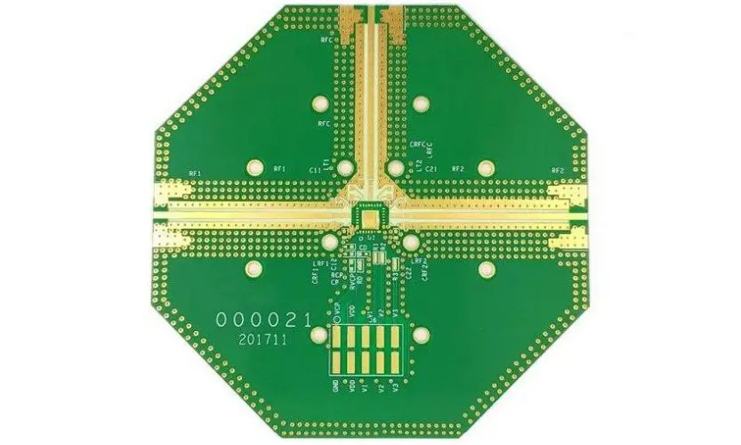
These partners also maintain expertise across various assembly technologies. Whether you need traditional through-hole assembly, advanced surface-mount technology, ball grid array (BGA) placement, or chip-on-board assembly, experienced providers have the right equipment and trained personnel. When we developed a product requiring 0201 components (incredibly tiny surface-mount devices measuring just 0.6mm x 0.3mm), our outsourcing partner handled it without hesitation. Attempting this in-house would have required new equipment and months of training.
Specialized Knowledge and Problem-Solving
One of the most valuable aspects of outsourcing is tapping into your partner’s accumulated knowledge. Experienced PCB assembly providers have seen thousands of designs and encountered virtually every assembly challenge imaginable. They can identify potential manufacturing issues during design review and suggest modifications that improve yield and reduce costs.
I recall a project where our engineering team designed a board with components placed too close together for automated assembly. Our assembly partner caught this during the DFM (Design for Manufacturing) review and suggested minor layout changes that prevented what would have been a 30% yield loss. Their expertise saved us from a costly mistake that our in-house team, despite their competence in design, simply didn’t have the assembly experience to foresee.
Quality Systems and Certifications
Reputable PCB assembly services maintain rigorous quality management systems and industry certifications that would be prohibitively expensive for most companies to achieve independently. ISO 9001, ISO 13485 (for medical devices), AS9100 (for aerospace), IATF 16949 (for automotive), and IPC certifications demonstrate a commitment to quality that provides peace of mind.
During my tenure in the medical device industry, we needed ISO 13485 certification for our assembly processes. Achieving this certification in-house would have required an 18-month effort, extensive documentation, facility upgrades, and annual audits. Our outsourcing partner already maintained this certification, allowing us to leverage their compliance framework and bring our product to market 12 months faster.
Benefit #3: Accelerated Time-to-Market and Scalability

In today’s competitive landscape, time-to-market can determine whether a product succeeds or fails. Outsourcing PCB assembly provides flexibility and speed that in-house operations struggle to match.
Rapid Production Ramp-Up
When you need to go from prototype to production, the timeline matters enormously. Setting up an in-house assembly line, even a modest one, typically requires 6-12 months when you factor in equipment procurement, facility preparation, staff hiring and training, and process validation. I’ve worked with PCB assembly partners who can transition from prototype to full production in as little as 2-4 weeks.
This speed proved critical for one of my most memorable projects—a consumer electronics product launching during the holiday season. Our original timeline had us starting production in May for October delivery. Due to design revisions, we didn’t finalize the product until July. An outsourcing partner with available capacity and experience in similar products helped us compress the production timeline, ultimately delivering on schedule. Attempting this in-house would have been impossible.
Flexible Scaling for Business Growth
Business demands fluctuate, and production capacity must adapt accordingly. With in-house assembly, you’re forced to choose between maintaining excess capacity (wasting resources during slow periods) or insufficient capacity (losing sales opportunities during peaks). Outsourcing elegantly solves this dilemma.
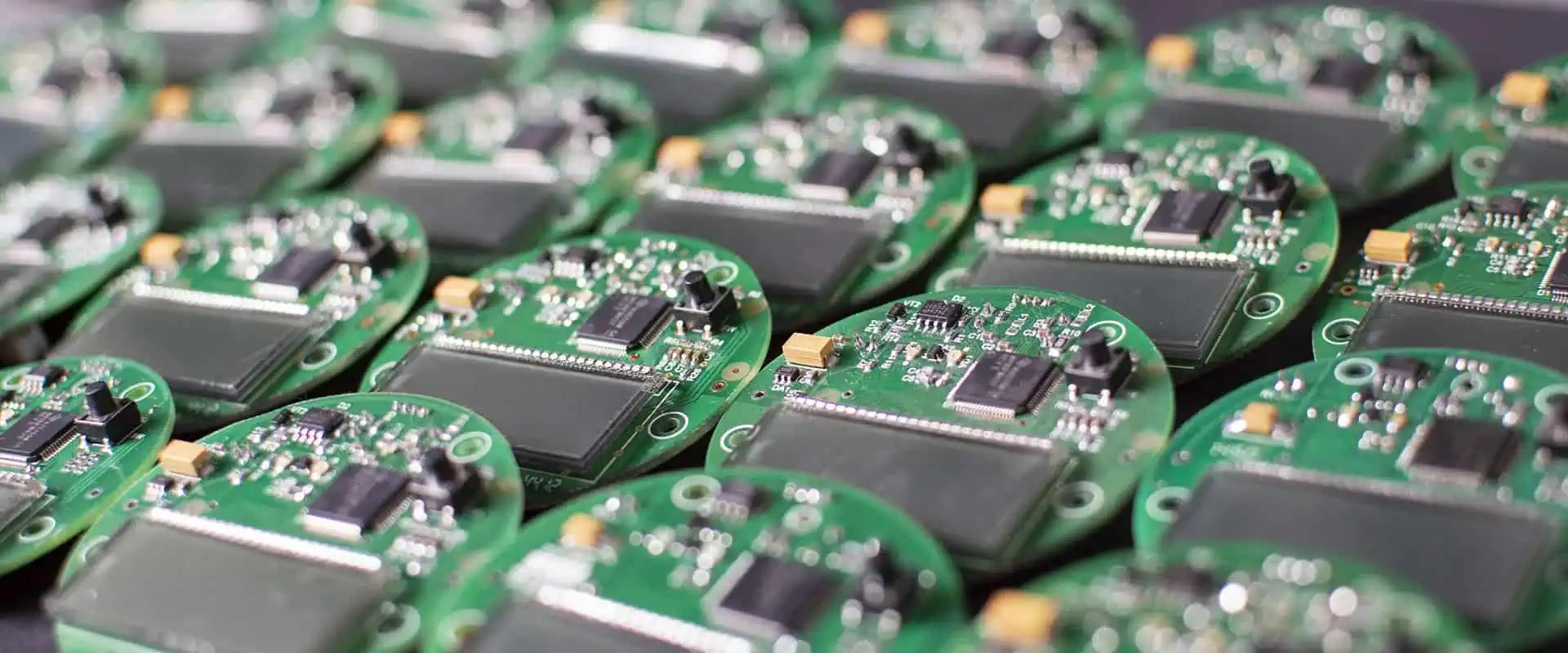
I currently manage electronics procurement for a company experiencing 200% year-over-year growth. Our PCB assembly partner has scaled with us seamlessly, from producing 1,000 units monthly in our first year to over 20,000 units today. They’ve allocated additional production lines, adjusted scheduling, and maintained consistent quality throughout this growth. Building this capacity internally would have required millions in investment and carried enormous risk if our growth trajectory changed.
Focus on Core Competencies
Perhaps the most strategic benefit of outsourcing is allowing your organization to focus on what it does best. Unless PCB assembly is your core business, managing it internally diverts attention and resources from activities that truly differentiate your company.
In my experience, the most successful electronics companies excel at product design, customer relationships, market positioning, or innovative features—not necessarily manufacturing. When we outsourced assembly, our engineering team stopped spending 30% of their time on manufacturing issues and redirected that effort toward next-generation product development. This focus accelerated our innovation cycle and strengthened our competitive position.
Benefit #4: Enhanced Risk Management and Quality Assurance
Manufacturing carries inherent risks—quality defects, supply chain disruptions, regulatory compliance, and technological obsolescence. Experienced PCB assembly partners help mitigate these risks through established systems and industry expertise.
Comprehensive Quality Control
Professional assembly services implement multi-stage quality control processes that catch defects early and prevent costly failures. These typically include incoming component inspection, solder paste inspection (SPI), automated optical inspection (AOI) after placement and reflow, X-ray inspection for hidden connections, in-circuit testing (ICT), and functional testing.
I learned the value of thorough quality control the hard way. Early in my career, working with a company doing in-house assembly, we shipped a batch of 500 units with a placement error that caused intermittent failures. The warranty claims, replacement costs, and damaged reputation cost us dearly. Since outsourcing to partners with comprehensive QC systems, our field failure rate has dropped by 85%.
Supply Chain Management and Component Procurement
PCB assembly requires procuring dozens or hundreds of different components from various suppliers. Managing these relationships, ensuring component authenticity, maintaining appropriate inventory levels, and navigating supply chain disruptions demands significant expertise and buying power.
Established assembly partners maintain relationships with authorized distributors and component manufacturers, providing access to better pricing and allocation during shortages. During the recent global chip shortage, our assembly partner’s established relationships and inventory management helped us maintain production while competitors faced months-long delays. Their purchasing power and expertise in component substitution proved invaluable.
Reduced Liability and Compliance Burden
Manufacturing carries legal responsibilities related to worker safety, environmental compliance, and product liability. Outsourcing transfers many of these risks to your assembly partner, who has specialized expertise in managing them.
This doesn’t mean you’re completely insulated from liability—you’re still responsible for your product’s design and performance. However, manufacturing-related issues like workplace accidents, environmental violations, or process-related defects become the assembly partner’s responsibility. The insurance requirements alone for manufacturing operations can be substantial; leveraging your partner’s coverage reduces your risk exposure.
Making the Outsourcing Decision: Practical Considerations
After outlining these four key benefits, I want to share some practical guidance for actually making the outsourcing decision and selecting the right partner.
When Does Outsourcing Make Sense?
Based on my experience, outsourcing PCB assembly typically makes strong sense when:
- Your annual production volume is under 100,000 units (above this, in-house may be economical)
- Your product design changes frequently, requiring assembly process flexibility
- You lack specialized assembly expertise in-house
- Capital is limited or better deployed elsewhere in your business
- You need to scale production quickly to meet market demands
- Your products require industry certifications you don’t currently maintain
Selecting the Right Assembly Partner
Not all PCB assembly services are equal. I evaluate potential partners using these criteria:
Technical Capabilities: Ensure they can handle your component types, board complexity, and volume requirements. Request capability statements and tour their facilities if possible.
Quality Systems: Verify appropriate certifications for your industry. Ask about defect rates, quality control processes, and how they handle non-conformances.
Communication: Responsive, clear communication is essential. During the vetting process, assess how quickly they respond and how well they understand your requirements.
Financial Stability: You’re entering a long-term partnership. Review their business history and financial health to ensure they’ll be around for your product’s lifecycle.
References and Reputation: Speak with current customers about their experiences. Online reviews provide some insight, but direct conversations reveal more.
Pricing Structure: Understand all costs including setup fees, component procurement markups, testing charges, and shipping. The lowest quote isn’t always the best value.
Conclusion: Strategic Advantage Through Smart Outsourcing
After years of managing electronics procurement and working with dozens of PCB assembly partners, I’m convinced that outsourcing is not just a cost-cutting measure—it’s a strategic advantage that enables companies to compete more effectively in today’s fast-paced market.
The four benefits I’ve outlined—cost reduction, access to advanced technology, accelerated time-to-market, and enhanced risk management—compound over time. The money you save on equipment and overhead can fund product development. The expertise you gain access to improves your designs. The time you save accelerates your innovation cycle. The risks you mitigate protect your business reputation.
That said, successful outsourcing requires finding the right partner and managing the relationship actively. Treat your PCB assembly service as a strategic partner, not just a vendor. Share your roadmap, communicate openly about challenges, and work collaboratively to optimize processes and costs.
Whether you’re producing your first prototype or scaling to meet explosive growth, the right PCB assembly partner can be the difference between struggling with manufacturing challenges and focusing on what truly drives your business forward. In my experience, that focus—on innovation, customers, and market opportunities—is what ultimately determines success in the competitive electronics industry.