A backplane is a high-speed printed circuit board that acts as the backbone of complex electronic systems like telecom, networking and industrial equipment. It provides interconnections between various cards and modules plugged into the system chassis. Designing reliable and optimized backplanes requires careful planning and execution to meet signal integrity, power delivery and mechanical challenges. This article provides a comprehensive guide on backplane PCB design covering architecture, layout considerations, material selection, analysis and validation steps.
Backplane Basics
Some fundamentals about backplane PCBs:
Provides interconnects between various PCBs and hardware units like line cards, switch fabric, storage modules etc. mounted on the chassis.
Enables high-speed data transfer and communication between modules using parallel bus interfaces like PCIe, Ethernet etc.
Contains multiple high-density board-to-board connectors to plug in cards and daughterboards.
Requires very careful impedance control and signal integrity design due to multi-GHz signal speeds.
Must handle significant power distribution to provide clean power to all modules.
Undergoes thermal and mechanical stresses requiring robust mechanical structure.
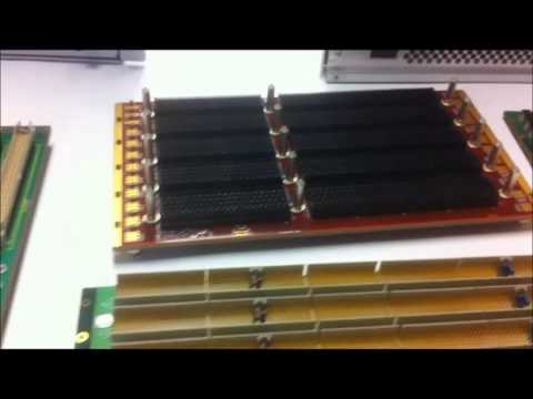
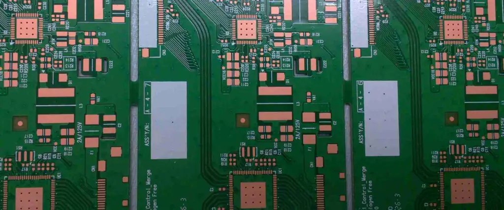
Fabricated using thick multilayer PCBs with 12+ layers typically.
Backplane Architecture
Defining the right backplane architecture is the first step:
Module Interconnect
Analyze inter-module data flow and bandwidth requirements.
Select suitable interconnect types like Ethernet, PCIe, proprietary buses etc.
Determine number of lanes, data rates, signaling levels etc. for each interface.
Connector Selection
Choose right angle or vertical mount connectors based on space availability.
Determine mounting type – press-fit, soldered, Z-axis elastomer etc.
Select connectors suited for target signal speeds and pin counts required.
Slot Planning
Define number and spacing of card slots based on modules.
Plan spacing for adequate airflow and cooling.
Form Factor and Dimensions
Select suitable backplane dimensions and board outline- ATCA, VME64x, cPCI etc.
Define positioning of power connectors, modules, card guides etc.
Designing reliable and high-performance backplane PCBs requires strong foundation in signal integrity, power distribution, electromagnetic compatibility and mechanical engineering. A structured approach covering architectural planning, electrical and mechanical design, prototyping, analysis and testing is key to develop complex backplanes successfully on tight schedules. With growth in data networks and modular systems, role of backplane continues to increase for interconnecting modern electronics systems.
FAQs
What are some examples of standard backplane form factors?
Some common form factors are CompactPCI, VMEbus, FASTBUS, Raceway, ATCA, VXS etc.
How is clock distributed in large backplane designs?
Clocks are distributed through balanced clock trees using traces, striplines and clock buffers for skews control and to minimize distortions.
What are some typical high-speed interfaces used in backplane?
PCI Express, 10Gb Ethernet, Infiniband, RapidIO, StarFabric, Serial ATA are commonly used backplane interfaces.
What type of connectors are suited for backplane applications?
High-density, high-speed board-to-board connectors like mezzanine, HDI and FCBGA types are commonly used on backplanes.
Why are backdrilled vias used extensively in backplane PCBs?
Backdrilling reduces via stubs allowing higher data rates and improved signal integrity for differential traces routed through vias.
Backplane PCBs: Introduction
Generally a Backplane PCB is a collection of multipleconnectors placed and connected on one PCB. By nature its responsibility is to carry signals like a cable from one connector to other but enough good health such as single0ended, differential paired signals, and power supply rails and return paths. The PCBs with semiconductor ICs are directly press-fit over a backplane PCB. These insertable cards or PCBs are called daughter cards. It makes the pins of sourceconnectors to be connected exactly on the required pinsof destination connectors.
A backplane PCB,in complexity is somehow similar to a motherboard PCB in respect of PCB design parameters but it has manydifferences in manufacturing process and functionality. A motherboard, well known to be densely routed signals board with high pin cunt semiconductor ICs. On the other enda backplane is considered an enough connectivity board on the “back” of boards. But a backplane PCB is much more than a connectivity board especially for high datarate communication systems. A backplane PCB transports allelectrical connectivity of signals and powersin between daughter boards.It also holds and supports daughter cards over it which can be press-fit or extract.
It increases throughput of system on the cost of increased design and manufacturing effort. Although, the early times backplanes do have wire-wrapped connectorsand sockets but data speed in newer systems has realized to utilize advance PCBs materials and manufacturing skills for backplane PCBs. It originated further PCB manufacturing constraints alongwith the existing ones. PC (Printed Circuit) based Backplanes are preferred over wire-wrapped backplanes due to their increased reliability and data carriage capability.In common practice Backplanes don’tcomprises of semiconductor chips over them. However, they have small electronic components like resistors, capacitors, filters and chassis ground circuitry over them.
Backplane Manufacturing Difficulties:
The Backplane PCBs have enhanced data throughput, signal travelling quality, ease of assembly and production but still it increased challenges for PCB manufacturers.
The Backplane PCB thickness increases because it consists of several high speed controlled impedance transmission lines, supply rail planes ad return paths.Transmission of high frequency data over longer traces requires wide signals traces to reduce signal attenuations. It needs thicker dielectric capable to maintain impedance and keep the signal absorption lowest. Increasing trace width decreases signal density in a layer in per unit area of PCB. On the other hand increasing dielectric thickness increases overall PCB thickness.
Insertion of more signal layers added to power planes and return planes increases layer count that finally approaches to 20 or even more.It becomes challenging to maintain standard thickness of PCB for a manufacturer with given materials and impedance matching parameters.
High speed fine PCB drilling for vias and connectors in backplanes works well till a thickness of 5 to 6mm. However, larger drill diameters are required for thicker PCBs. Higher drill aspect ratios such as 8:1 constraints manufacturer to volumetric production so thicker PCBs require multiple drill passes for a single via.
It is a common practice to through daughter cared input power supplies by backplanes for examples ±5V, ±12V and ±24V DC. Many a times each power rail needs a separate return path plane to reduce PCB commotion. In such a way it may need upto 12-layers for power supplies.Framework computers having high current power supplies which produce IR losses over the planes copper. Thatneedsheat sinks or heat radiator fans for temperature compensation. Their leading layers need thicker copper compared to other internal layers.With higher layer count PCB layer registration, via alignment, pad-hole alignment and pressing a thicker PCB also becomes difficult.
Overall a high-speed backplane PCB increases entire manufacturing process through routing complexity, etching, layer registration, thickness, weight, material selection, and cost and production process.
PCB Pressing
In thicker backplanes manufacturing drilling becomes more complicated. A lengthy drill hole requires multiple times drilling the hole. It decreases drilling accuracy ad PCB yield percentage. It degrades high frequency performance.
High density etching
In a backplane PCB due to high count of connectors so their mounting holes and pads use significant part of PCB real-estate. The PCB designers strive to increase signal routing density maintaining impedance, trace length, instead of increasing number of layers. The increased signals density increases etching complexity. It pushes the trace, via-hole, pad-hole, annular ring geometries to the fabrication tolerance limits.
Impedance matching
With high speed data transmissions in the backplane PCBs impedance matched PCB fabrication becomes a challenge.Data transmission in GB per second range is generally not recommended over general FR-4 materials. The dielectric constant and dissipation factor dictate the material selection for backplane PCBs. This creates a challenge for PCB manufacturer to provide PCBs on demanded materials. The transmission line impedance, via impedance and connector pad to pin impedance also becomes a challenge. A new material type needs PCB manufacturing process to be slightly amendedat manufacturer facility.
As unused copper piece in PCB can act as stub in high frequency signals.The similar stub-effect may occur due to unused via barrel copper and annular ring. For this purpose PCB manufacturers are pushed to back-drill PCB. It requiresremoving the redundant via barrel from a thru-hole via in a PCB. The manufacturer removes thatvia copper after PCB fabrication is complete byre-drilling the target holes with a different drill size, leaving a certain length after last layer connection. It slows the production and causes inaccuracies in PCBs.
Connectors Alignment
A high speed backplane has good impedance matched connectors over it. In general a backplane has around 50 impedance controlled differential pairs per square inch. So the total differential pair length approaches to 500 pairs in a plane.The high density SMD and through-hole connectors allow smaller PCB size but they need many blind press-fit insertion and extraction of daughter cards from it. It harmsdurability of PCB. The manufacturerconstraint arises to maintain a hole-locations and geometry of connectors as well as maintaining the signal integrity throughout the PCB.
Layer registration
Layer registration in high speed high density PCBs causes low accuracy during copper etching, lamination, drilling and dimensional stability. The signal integrity and PCB yield at smaller sizes becomes more challenging for manufacturer.
Aspect ratio is the ratio of drill size to PCB thickness. Dense signals routing,higher copper layers count, and high vias and connector through-holes count in a backplane makes itsaspect ratio high that leads manufacturingdifficulties.PCB design engineers strive to maintain an acceptable ratio figure effective for PCB assembly china and durability. Manufacturers are pushedto manufacture PCBs with 10:1 aspect ratio. However, 6:1 aspect ratio is a common number.
Other common problems which are related to backplane PCBs manufacturing of backplane PCBs are CAF (copper anodic filament), impractical stackups (such as odd-numbered layers PCB design), thickness control of multilayer PCB and high-pressure compression, incomplete manufacturing information, incorrect blind and buried vias placement, improper layer-pairs, environmental impacts on PCB core and pre-preg materials, stringentrequirementsforced by international body regulations.
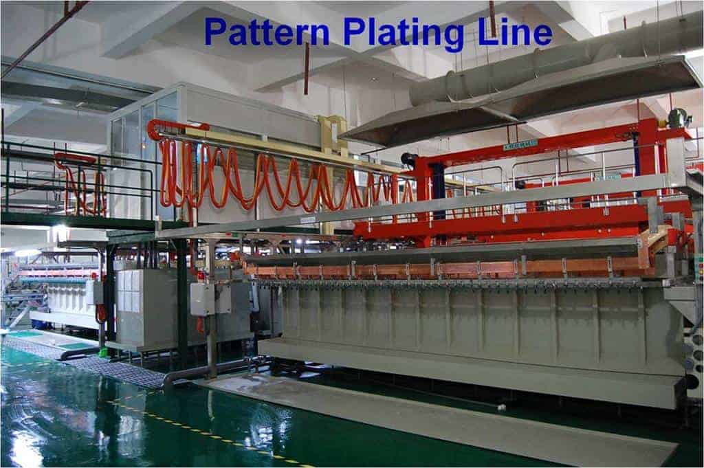
Electroplating is a key process used during the manufacturing of printed circuit boards (PCB) to deposit metallic coatings on the substrate. It involves electrodeposition of a thin film of metal like copper, tin, nickel, gold etc. onto the PCB to build up the conductive traces and interconnects. In this article, we will learn the basics of electroplating and its role in PCB fabrication.
Why Electroplating is Used in PCBs?
Electroplating provides the following benefits for PCB manufacturing:
Enables depositing uniform, smooth and dense metal coatings.
Allows building up PCB copper thickness up to 1 oz/ft2 or higher.
Deposits can be precisely controlled by process parameters.
Conformal step coverage into small openings and vias.
Cost-effective process with high throughput.
Suitable for plating a wide range of metals like Cu, Sn, Ni, Au etc.
Environmentally cleaner compared to many coating processes.
Thus, electroplating is ideally suited for metallization of PCBs during fabrication.
Electroplating involves applying a voltage between two electrodes immersed in a salt solution (electrolyte) to drive metal deposition onto the cathode surface.
Key Components
Anode – Positive electrode providing metal ions into the solution. Made of the metal being plated.
Cathode – Negative electrode to be plated. The PCB acts as the cathode.
Electrolyte – Contains aqueous solution of metal salts and other additives.
Power Supply – Applies direct current between electrodes.
Basic electroplating process setup showing anode, cathode, electrolyte and power supply.
Mechanism
When a DC voltage is applied, the metal atoms of the anode dissolve into the electrolyte as positive ions.
The PCB substrate acting as cathode is charged negatively. This attracts the positively charged metal ions in the electrolyte to deposit onto the PCB surfaces forming a thin metal coating.
Electroplating in PCB Fabrication
Electroplating is utilized at multiple stages during the manufacture of a printed circuit board:
1. Copper Electroplating
After drilling and desmear, copper is electroplated to build up traces on the PCB.
Multiple plating cycles with increasing thickness are used to reach final copper thickness.
Plating rates up to 1 mil/min can be achieved.
2. Tin-Lead or Tin Electroplating
Tin-lead or pure tin plating applied on surface pads for solderability.
Provides good solderability for SMT component assembly.
3. Nickel and Gold Plating
Nickel plating applied over copper traces for corrosion protection.
Some benefits of using electroplating for PCB fabrication:
Produces uniform metal coatings with good dimensional control.
Allows building up of copper thickness to over 1 oz.
Recesses and vias can be covered through optimal throwing power.
Reduces porosity in the metal deposit.
Operates at close to room temperatures.
Provides high production rate and throughput.
Lower cost compared to some physical vapor deposition techniques.
Simpler equipment and setup compared to CVD, PVD.
Allows depositing a wide range of metals.
Limitations of Electroplating
Some limitations of electroplating include:
Metal purity is lower compared to vapor deposition techniques.
Plating thickness inside openings falls as aspect ratio increases.
Requires additional processing steps for resist patterning.
Stripping and cleaning steps produce liquid effluents.
Corrosion and maintenance requirements of electrolyte bath and anodes.
Metals like aluminum cannot be electroplated.
Difficulty plating non-conductive substrates without seed layer.
Conclusion
Electroplating is an efficient and cost-effective process that enables metallization of printed circuit boards during fabrication. It allows depositing a wide range of metals like copper, tin, nickel to build the conductive traces and interconnects on the PCB substrate. By selecting optimal process parameters and electrolyte composition, electroplating provides an ideal solution for metallization of PCBs in a high volume manufacturing environment.
FAQs
How is electrolytic copper different from electroless copper plating?
Electrolytic copper requires applying external current while electroless copper relies on auto-catalytic chemical process without external power.
What are some surface finishes deposited by electroplating on PCBs?
Common PCB surface finishes plated include tin, tin-lead, nickel, gold, silver and palladium-nickel coatings.
What defects can occur during electroplating?
Burning, pitting, nodulation, cracking, peeling, contamination, over/under-plating are some common electroplating defects.
Why is pattern plating done for PCB fabrication?
Pattern plating allows selective electroplating only in desired conductor pattern. This eliminates need to etch away unwanted copper after plating.
What are auxiliary anodes used for in PCB electroplating?
Auxiliary anodes placed near edges/corners compensate for low current densities in those areas and enable more uniform plating thickness.
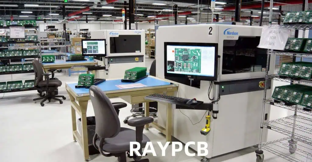
In the ever-evolving landscape of electronics manufacturing, Printed Circuit Board (PCB) inspection stands as a cornerstone of quality assurance. As we approach 2025, the importance of robust PCB inspection processes has never been more critical. But what exactly is PCB inspection, and why does it matter so much in modern electronics production?
PCB inspection is the systematic examination of printed circuit boards to ensure they meet design specifications, quality standards, and functional requirements. This process is vital in identifying defects, inconsistencies, and potential failure points before a PCB is integrated into a final product. With the increasing complexity of electronic devices and the demand for higher reliability across industries, PCB inspection has become an indispensable step in the manufacturing process.
This comprehensive guide will delve into the methods, techniques, and best practices of PCB inspection as we look ahead to 2025. We’ll explore the various inspection technologies available, from traditional visual inspections to cutting-edge automated systems. Moreover, we’ll discuss why PCB inspection is more crucial than ever, given the trends towards miniaturization and the stringent quality requirements in sectors like automotive, aerospace, and medical devices.
As PCBs continue to grow in complexity, with denser component placement and finer traces, the need for advanced inspection techniques has risen correspondingly. This guide aims to equip manufacturers, engineers, and quality control professionals with the knowledge to navigate the challenges and opportunities in PCB inspection, ensuring the production of high-quality, reliable electronic products in the years to come.
PCB inspection is a critical quality control process in electronics manufacturing that involves examining printed circuit boards for defects, errors, and compliance with design specifications. The primary purpose of PCB inspection is to ensure that each board meets the required standards of quality and functionality before it moves on to the next stage of production or is integrated into a final product.
Importance in Quality Control and Product Reliability
The significance of PCB inspection in maintaining quality control and enhancing product reliability cannot be overstated. Here’s why it’s so crucial:
Defect Detection: Early identification of issues allows for timely corrections, reducing the risk of product failure in the field.
Cost Reduction: Catching problems early in the production process is far less expensive than dealing with failures in assembled products or returns from customers.
Yield Improvement: Regular inspection helps identify recurring issues, allowing for process improvements that increase overall production yield.
Compliance Assurance: Inspection ensures that PCBs meet industry standards and regulatory requirements, which is crucial for sectors like medical devices and aerospace.
Customer Satisfaction: Reliable products lead to satisfied customers and a stronger brand reputation.
Common Defects Detected Through PCB Inspection
PCB inspection processes are designed to catch a wide range of potential defects. Some of the most common issues include:
Soldering Problems:
Solder bridges (unwanted connections between solder points)
Insufficient solder
Cold solder joints
Solder voids
Component Issues:
Misaligned or missing components
Incorrect component placement
Wrong polarity
Damaged components
PCB Substrate Defects:
Cracks or breaks in the board
Delamination
Warpage
Trace and Pad Defects:
Open circuits
Short circuits
Lifted pads
Broken traces
Manufacturing Residues:
Flux residue
Foreign material contamination
Dimensional Issues:
Incorrect board thickness
Misaligned drill holes
By effectively identifying these and other defects, PCB inspection plays a pivotal role in ensuring the quality and reliability of electronic products.
2. Why PCB Inspection Matters More Than Ever in 2025
As we approach 2025, several factors are converging to make PCB inspection more critical than ever before. Let’s explore the key reasons why this process has become increasingly important in the electronics manufacturing landscape.
Increasing Miniaturization of Electronics
The trend towards smaller, more compact electronic devices continues unabated. This miniaturization presents several challenges for PCB manufacturing and inspection:
Denser Component Placement: With more components packed into smaller spaces, the risk of defects like solder bridges or misalignments increases.
Finer Traces and Smaller Vias: As PCB features become smaller, they become more difficult to inspect visually, requiring more advanced inspection techniques.
Increased Complexity: Multi-layer boards with intricate designs are becoming more common, necessitating more thorough inspection processes.
Demand for Higher Reliability
Certain industries have always demanded high reliability from their electronic components. However, this requirement is now spreading to a broader range of sectors:
Automotive Industry: With the rise of electric and autonomous vehicles, the number of PCBs per vehicle is increasing, and each must meet stringent reliability standards.
Aerospace: PCBs used in aircraft and spacecraft must withstand extreme conditions and have near-zero failure rates.
Medical Devices: From implantable devices to diagnostic equipment, medical PCBs require exceptional reliability to ensure patient safety.
Consumer Electronics: As devices become more integral to daily life, consumers expect longer-lasting, more reliable products.
Compliance with International Standards
The regulatory landscape for electronics manufacturing is becoming increasingly complex. Rigorous PCB inspection is essential for compliance with various standards:
IPC-A-610: This standard for PCB assembly has become more stringent in its latest revisions.
ISO 9001: Quality management systems require thorough inspection processes.
Industry-Specific Standards: Different sectors (e.g., medical, automotive) have their own stringent requirements.
Proper inspection ensures that PCBs meet these standards, avoiding costly non-compliance issues.
Cost Savings: Early Detection Reduces Rework and Scrap Rates
In 2025, with increasing pressure on profit margins, the financial benefits of thorough PCB inspection are more apparent than ever:
Reduced Rework: Catching defects early in the production process is far less expensive than reworking assembled products.
Lower Scrap Rates: Effective inspection minimizes the number of PCBs that must be discarded due to undetected defects.
Warranty Cost Reduction: Fewer field failures mean lower warranty claim costs and better customer satisfaction.
Process Improvement: Data from inspections can be used to refine manufacturing processes, leading to long-term cost savings.
Adaptation to New Materials and Technologies
As new PCB materials and manufacturing technologies emerge, inspection processes must evolve to address unique challenges:
Flexible and Rigid-Flex PCBs: These require specialized inspection techniques to ensure quality across different materials and bending points.
High-Frequency PCBs: Used in 5G and other advanced applications, these boards require precise impedance control and tight tolerances, necessitating advanced inspection methods.
Embedded Components: As more PCBs incorporate embedded passive and active components, inspection must adapt to verify these hidden elements.
Environmental Considerations
With growing emphasis on sustainability, PCB inspection plays a role in environmental responsibility:
Energy Efficiency: Ensuring PCBs are correctly manufactured contributes to the energy efficiency of the final products.
Compliance with Environmental Regulations: Proper inspection helps ensure adherence to regulations like RoHS and REACH.
In conclusion, as we look towards 2025, PCB inspection is not just a quality control measure but a critical process that impacts product reliability, regulatory compliance, financial performance, and environmental responsibility. The increasing complexity of electronic devices, coupled with higher expectations for performance and longevity, makes robust PCB inspection more important than ever in ensuring the success of electronics manufacturing ventures.
As PCB technology advances, so do the methods used to inspect them. In 2025, manufacturers have a range of inspection techniques at their disposal, each with its own strengths and ideal applications. Let’s explore the primary types of PCB inspection methods.
3.1 Manual Visual Inspection (MVI)
How it Works
Manual Visual Inspection (MVI) is the most traditional form of PCB inspection. It involves trained inspectors visually examining PCBs for defects, often with the aid of magnification tools.
Tools Used:
Magnifying glasses
Stereo microscopes
Illuminated magnifiers
High-resolution cameras with display screens
Pros and Cons
Pros:
Low initial investment
Effective for detecting visible surface defects
Flexible and adaptable to different PCB types
Can catch unexpected or unusual defects that automated systems might miss
Cons:
Time-consuming, especially for complex boards
Subject to human error and fatigue
Inconsistent results between different inspectors
Limited effectiveness for small components or hidden defects
Best Practices to Improve Accuracy
Proper Lighting: Use adjustable, high-quality lighting to enhance visibility of defects.
Regular Breaks: Implement scheduled breaks to combat eye strain and fatigue.
Standardized Procedures: Develop and follow consistent inspection checklists and procedures.
Ongoing Training: Regularly train inspectors on new components and potential defects.
Ergonomic Workstations: Design inspection areas to minimize physical strain on inspectors.
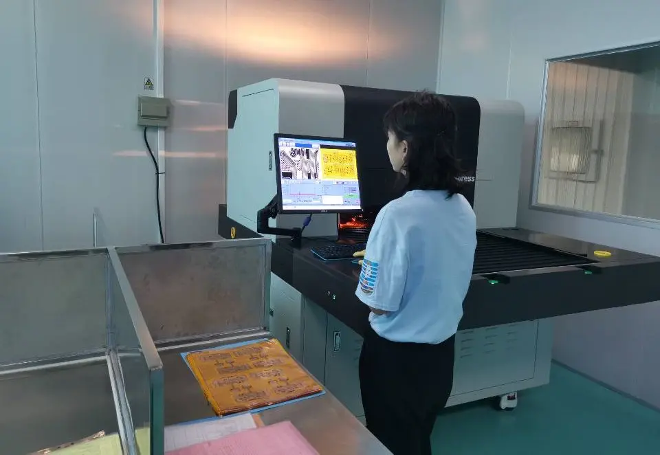
3.2 Automated Optical Inspection (AOI)
Principles of AOI Technology
Automated Optical Inspection uses cameras and image processing software to automatically detect defects on PCBs. It compares captured images of the PCB against a known good board or CAD data to identify anomalies.
Inline vs Offline AOI
Inline AOI: Integrated directly into the production line, inspecting boards as they move through the manufacturing process.
Offline AOI: Separate from the production line, used for more detailed inspection or for smaller production runs.
2D vs 3D AOI in 2025: Latest Advances
2D AOI: Traditional method, effective for detecting surface-level defects.
3D AOI: Uses multiple cameras or laser technology to create a three-dimensional image of the PCB, allowing for more accurate inspection of component height, coplanarity, and solder joint quality.
Latest Advances:
Higher resolution cameras for detecting smaller defects
Improved AI algorithms for defect classification
Integration with factory automation systems for real-time process control
Speed: Can inspect hundreds of points per second, much faster than manual inspection.
Repeatability: Consistent results across multiple inspections and different boards.
High Defect Detection Rates: Can detect a wide range of defects with high accuracy.
Data Collection: Provides valuable data for process improvement and traceability.
3.3 X-ray Inspection (AXI)
When and Why to Use X-ray Inspection
X-ray inspection is crucial for examining internal structures of PCBs and components that are not visible to optical inspection methods. It’s particularly useful for:
Inspecting BGAs (Ball Grid Arrays) and other hidden solder joints
Checking for voids in solder connections
Examining multi-layer boards for internal defects
Detecting Hidden Defects
AXI can detect a variety of hidden defects, including:
Solder bridges under BGA components
Voids in solder joints
Misalignment of internal layers in multi-layer PCBs
Broken internal connections or vias
Differences Between 2D, 2.5D, and 3D X-ray Inspections
2D X-ray:
Provides a top-down view of the PCB
Useful for basic solder joint inspection
Limited in detecting issues in overlapping components
2.5D X-ray:
Combines multiple 2D images taken at different angles
Offers better visibility of solder joints under components
Improves detection of solder voids and bridges
3D X-ray (Computed Tomography):
Creates a full three-dimensional model of the PCB
Allows for “slicing” through the board to examine specific layers
Highest level of defect detection, especially for complex, multi-layer boards
3.4 Flying Probe Testing (FPT)
How Flying Probe Systems Work
Flying Probe Testing uses mobile test probes to make contact with specific points on the PCB, checking for electrical continuity and component values. The probes “fly” from point to point based on the PCB design data.
Ideal Applications: Prototypes, Low-Volume Production
FPT is particularly well-suited for:
Prototype PCBs where creating a dedicated test fixture isn’t cost-effective
Low-volume production runs
Complex boards with dense component placement
Boards that undergo frequent design changes
Key Advantages:
No need for expensive, custom test fixtures
Highly flexible, easily adaptable to different PCB designs
Can test hard-to-reach points on densely populated boards
3.5 In-Circuit Testing (ICT)
How ICT Differs from Flying Probe Testing
In-Circuit Testing uses a bed-of-nails fixture, a custom-made array of pins that makes contact with specific points on the PCB simultaneously. This allows for faster testing compared to Flying Probe methods.
Rapid test execution, often just a few seconds per board
Comprehensive testing of both passive and active components
Ability to detect both manufacturing defects and component failures
High repeatability and consistency in test results
Considerations:
Requires a custom fixture for each PCB design, which can be costly
Less flexible than FPT for design changes
May have limitations for very densely packed boards
3.6 Functional Testing (FCT)
End-Product Functionality Validation
Functional Testing goes beyond checking individual components or connections. It validates that the PCB performs its intended functions as part of the final product.
Where Functional Testing Fits in the Inspection Process
FCT typically occurs after other inspection methods, often as one of the final steps before the PCB is integrated into the end product. It can include:
Powering up the board and checking for correct voltage levels
Testing communication interfaces (e.g., USB, Ethernet)
Verifying sensor inputs and actuator outputs
Running software-based tests to check overall functionality
Importance:
Catches issues that might be missed by other inspection methods
Ensures the PCB will work correctly in its intended application
Can simulate real-world conditions to test durability and performance
In 2025, a comprehensive PCB inspection strategy often involves a combination of these methods, tailored to the specific requirements of the product, production volume, and quality standards. By leveraging the strengths of each inspection technique, manufacturers can ensure the highest level of quality and reliability in their PCB production.
4. Techniques and Tools for Effective PCB Inspection
As we delve deeper into the world of PCB inspection, it’s crucial to understand the specific techniques and tools used to ensure the quality and reliability of printed circuit boards. In 2025, these methods have become more sophisticated, leveraging advanced technologies to detect even the most minute defects. Let’s explore some of the key techniques and tools used in effective PCB inspection.
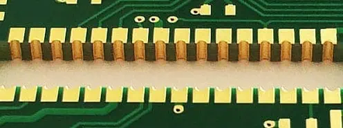
4.1 Solder Joint Inspection
Solder joint quality is paramount in PCB manufacturing, as poor solder joints are a common cause of PCB failure. Here are some techniques for identifying various solder joint issues:
Techniques for Identifying Solder Bridges, Voids, and Cold Joints
Visual Inspection for Solder Bridges:
Use high-magnification cameras or microscopes to detect unwanted connections between solder points.
Look for excess solder forming a bridge between adjacent pads or leads.
X-ray Inspection for Voids:
Employ X-ray systems to detect voids within solder joints, especially for hidden joints like those in BGAs.
Analyze X-ray images for dark spots within the solder, indicating air pockets or voids.
Thermal Imaging for Cold Joints:
Use infrared cameras to detect temperature differences that may indicate cold solder joints.
Look for joints that heat up more slowly or to a lower temperature than surrounding joints.
3D AOI for Solder Joint Profile:
Utilize 3D AOI systems to create a three-dimensional model of solder joints.
Analyze the shape and volume of solder to ensure proper formation an
Cross-Sectioning for In-Depth Analysis:
For critical applications or troubleshooting, use physical cross-sectioning of solder joints.
Examine the internal structure of joints to assess intermetallic compound formation and void distribution.
4.2 Trace and Pad Inspection
Ensuring the integrity of PCB traces and pads is crucial for the overall functionality and reliability of the board. Here are key techniques for this aspect of inspection:
Importance of Checking PCB Traces, Vias, and Pads for Continuity and Quality
Automated Optical Inspection (AOI) for Surface Traces:
Use high-resolution cameras to detect breaks, narrowing, or other defects in surface traces.
Compare against CAD data to ensure trace width and spacing meet design specifications.
X-ray Inspection for Internal Layers:
Employ X-ray systems to examine traces and vias in internal layers of multi-layer PCBs.
Look for disconnections, misalignments, or other defects not visible from the surface.
Electrical Testing for Continuity:
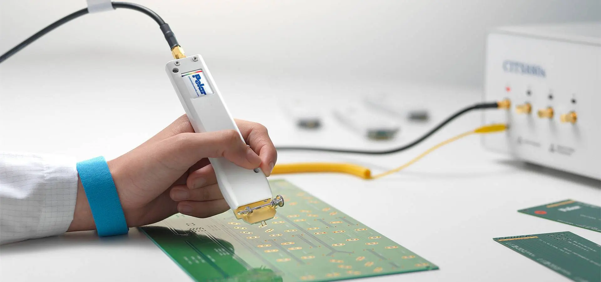
Use flying probe or in-circuit testers to verify electrical continuity of traces and vias.
Check for opens, shorts, and resistance values that fall outside acceptable ranges.
3D Profilometry for Pad Height and Coplanarity:
Utilize laser or structured light 3D scanning to measure pad height and ensure coplanarity.
Verify that pads meet specifications for subsequent assembly processes like component placement.
Microsectioning for Via Quality:
For critical applications, perform microsectioning to examine the internal structure of vias.
Assess plating thickness, void presence, and overall via formation quality.
4.3 Component Placement and Polarity Verification
Ensuring correct component placement and polarity is essential for PCB functionality. Here are techniques to detect misplaced or rotated components:
How to Detect Misplaced or Rotated Components
2D AOI for Component Presence and Position:
Use pattern matching algorithms to verify component presence and correct positioning.
Compare component outlines and markings against reference images.
3D AOI for Component Height and Coplanarity:
Employ 3D scanning to measure component height and ensure proper seating on the board.
Check for tilted or lifted components that may indicate placement issues.
Fiducial Recognition for Alignment Verification:
Utilize fiducial markers on the PCB to verify overall alignment accuracy of component placement.
Ensure components are placed within specified tolerances relative to these reference points.
Polarity Checking with OCR and Pattern Matching:
Use Optical Character Recognition (OCR) to read component markings and verify correct orientation.
Employ pattern matching to check for polarity indicators like diode bands or pin 1 markers.
X-ray Inspection for Hidden Components:
Use X-ray systems to verify correct placement and orientation of BGAs and other hidden components.
Check for proper alignment of internal structures like solder balls or lead frames.
4.4 3D Inspection Technologies
As PCBs become more complex, 3D inspection technologies have become increasingly important. Here’s an overview of the latest advancements:
Use of 3D Profilometry and Laser Measurement in 2025
Structured Light 3D Scanning:
Projects a pattern of light onto the PCB surface and analyzes its deformation to create a 3D model.
Provides high-resolution data on surface topography, component height, and solder joint profiles.
Laser Triangulation:
Uses laser line projection and camera imaging to create precise 3D measurements.
Excellent for measuring component height, coplanarity, and solder paste volume.
Confocal Microscopy:
Employs optical sectioning to create high-resolution 3D images of small features.
Useful for inspecting fine-pitch components and analyzing surface textures.
Multi-Angle and Multi-Spectral Imaging:
Combines images from multiple angles and light spectra to create comprehensive 3D models.
Enhances defect detection capabilities, especially for complex geometries and varied materials.
AI-Enhanced 3D Analysis:
Utilizes machine learning algorithms to interpret 3D scan data and identify defects.
Improves detection accuracy and reduces false positives in 3D inspection processes.
These advanced 3D inspection technologies allow for more precise measurements and better detection of defects related to component placement, solder joint quality, and overall board topology. They are particularly valuable for inspecting complex, densely populated PCBs and for ensuring compliance with increasingly stringent manufacturing standards.
By employing these techniques and tools, PCB manufacturers can significantly enhance their inspection capabilities, ensuring higher quality products and reducing the risk of field failures. As we move further into 2025 and beyond, we can expect these technologies to become even more sophisticated, with increased integration of AI and machine learning to further improve defect detection and process control in PCB manufacturing.
5. Common PCB Defects Found During Inspection
As PCB designs become more complex and manufacturing processes more advanced, the types of defects that can occur during production have also evolved. In 2025, PCB inspection processes are designed to catch a wide array of potential issues. Understanding these common defects is crucial for maintaining high-quality standards in PCB manufacturing. Let’s explore the main categories of defects typically found during PCB inspection:
Description: Unintended connections between circuit points.
Causes: Solder bridges, conductive contamination, or design errors.
Detection: In-circuit testing, flying probe testing, and power-on testing.
Open Circuits:
Description: Breaks in intended electrical pathways.
Causes: Broken traces, lifted pads, or incomplete solder joints.
Detection: Electrical continuity testing, flying probe testing, and functional testing.
High Resistance Connections:
Description: Connections with higher than expected resistance.
Causes: Poor soldering, oxidation, or partial breaks in traces.
Detection: Precision resistance measurement, thermal imaging during power-on.
Leakage Currents:
Description: Unintended current flow between isolated circuit sections.
Causes: Contamination, moisture ingress, or insulation breakdown.
Detection: Insulation resistance testing, specialized leakage current tests.
Additional Common Defects
Solder Paste Issues:
Insufficient or excess solder paste
Smeared or misaligned solder paste deposits
Detection: Solder paste inspection (SPI) systems
Via Defects:
Incomplete plating
Voids in via fill
Detection: X-ray inspection, microsectioning for critical applications
Pad Lift-Off:
Description: Separation of copper pads from the PCB substrate
Causes: Excessive heat during rework, poor adhesion in manufacturing
Detection: Visual inspection, stress testing
Tombstoning:
Description: One end of a component lifts off the pad during soldering
Causes: Uneven heating, pad design issues, or component placement problems
Detection: AOI, visual inspection
Foreign Object Debris (FOD):
Description: Unwanted particles or objects on the PCB
Causes: Contamination during manufacturing or handling
Detection: Visual inspection, AOI
Understanding these common defects is crucial for developing effective inspection strategies and improving overall PCB quality. In 2025, the integration of AI and machine learning into inspection systems is enhancing the ability to detect and classify these defects accurately and efficiently. This not only improves the quality of individual PCBs but also provides valuable data for continuous improvement of the manufacturing process.
6. Best Practices for PCB Inspection in 2025
As we navigate the complexities of PCB manufacturing in 2025, implementing best practices in inspection processes is crucial for ensuring high-quality, reliable products. These practices not only help in detecting defects but also in preventing them and optimizing the overall manufacturing process. Let’s explore the key best practices for PCB inspection:
Design for Inspection (DFI): Designing PCBs with Inspection in Mind
Incorporate Test Points:
Include dedicated test points in PCB designs to facilitate easier electrical testing.
Ensure test points are accessible for both automated and manual inspection methods.
Optimize Component Placement:
Design layouts that allow for clear visual access to components and solder joints.
Avoid placing small components under larger ones where possible.
Use Fiducial Markers:
Include fiducial markers to aid in alignment during automated inspection processes.
Place fiducials strategically for maximum effectiveness in component placement verification.
Consider X-ray Inspection Requirements:
For boards with BGAs or other hidden solder joints, design with X-ray inspection in mind.
Avoid overlapping components that could obscure X-ray views of critical areas.
Standardize Pad Designs:
Use consistent pad designs where possible to simplify automated inspection programming.
Ensure pad sizes and shapes are optimized for both soldering and inspection processes.
Choosing the Right Inspection Method Based on Volume, Complexity, and Cost
Assess Production Volume:
For high-volume production, invest in automated systems like AOI and AXI.
For low-volume or prototype runs, consider more flexible options like flying probe testing.
Evaluate Board Complexity:
For complex, multi-layer boards, incorporate X-ray inspection into the process.
Use 3D AOI for boards with a high mix of component types and sizes.
Consider Cost-Effectiveness:
Balance the cost of inspection equipment against the potential cost of field failures.
Factor in the long-term benefits of data collection and process improvement capabilities.
Adapt to Product Lifecycle:
Implement more rigorous inspection processes during new product introduction phases.
Adjust inspection strategies as products mature and processes stabilize.
Combining Multiple Inspection Methods for Maximum Reliability
Implement a Multi-Stage Inspection Process:
Use SPI (Solder Paste Inspection) before component placement.
Follow with AOI after placement and reflow.
Incorporate AXI for critical or hidden joints.
Finish with ICT or functional testing.
Tailor Inspection Combinations to Product Requirements:
For high-reliability products (e.g., medical, aerospace), use a combination of visual, AOI, AXI, and electrical testing.
For consumer electronics, balance speed and cost with an appropriate mix of automated and sampling-based inspections.
Use Data Integration:
Implement systems that allow data sharing between different inspection stages.
Utilize this integrated data for comprehensive defect analysis and process improvement.
Training and Certification for Inspection Personnel
Develop Comprehensive Training Programs:
Provide in-depth training on PCB technology, common defects, and inspection equipment.
Include hands-on practice with a variety of PCB types and potential defects.
Pursue Industry Certifications:
Encourage staff to obtain relevant certifications (e.g., IPC Certification).
Support ongoing education to keep up with evolving technologies and standards.
Implement Regular Skill Assessments:
Conduct periodic evaluations of inspector performance and knowledge.
Use results to tailor ongoing training and development programs.
Foster a Culture of Continuous Learning:
Encourage knowledge sharing among team members.
Provide opportunities for inspectors to learn about new technologies and industry trends.
Maintaining and Calibrating Inspection Equipment
Establish Regular Calibration Schedules:
Develop and adhere to calibration schedules for all inspection equipment.
Use traceable standards for calibration processes.
Perform Routine Maintenance:
Implement preventive maintenance programs for all inspection systems.
Keep detailed maintenance logs and track equipment performance over time.
Verify Equipment Accuracy:
Regularly use known good boards and known defect boards to verify inspection system performance.
Adjust and fine-tune systems as needed based on these verifications.
Stay Current with Software Updates:
Keep inspection system software up-to-date to benefit from the latest algorithms and features.
Evaluate and implement new software capabilities that can enhance inspection accuracy or efficiency.
Monitor Environmental Conditions:
Ensure inspection areas maintain stable temperature and humidity levels.
Use environmental monitoring systems to track and log conditions that could affect inspection accuracy.
Implementing Continuous Improvement Processes
Analyze Inspection Data:
Regularly review data from all inspection stages to identify trends and recurring issues.
Use statistical process control (SPC) methods to monitor and improve manufacturing processes.
Conduct Root Cause Analysis:
For significant or recurring defects, perform thorough root cause analysis.
Implement corrective actions based on these analyses to prevent future occurrences.
Foster Collaboration Between Departments:
Encourage regular meetings between design, manufacturing, and quality control teams.
Use inspection findings to inform design improvements and manufacturing process adjustments.
Benchmark Against Industry Standards:
Regularly compare your inspection processes and results against industry benchmarks.
Participate in industry forums and associations to stay informed about best practices.
Invest in New Technologies:
Stay informed about advancements in inspection technologies.
Evaluate and implement new technologies that can improve inspection accuracy or efficiency.
7. Trends Shaping the Future of PCB Inspection
As we look towards the future of PCB inspection, several key trends are emerging that promise to revolutionize the field. These advancements are not only improving the accuracy and efficiency of inspection processes but also transforming how manufacturers approach quality control in PCB production. Let’s explore the major trends shaping the future of PCB inspection in 2025 and beyond.
AI and Machine Learning in Automated Inspections
Artificial Intelligence (AI) and Machine Learning (ML) are rapidly becoming integral parts of PCB inspection systems, offering unprecedented levels of accuracy and efficiency.
Advanced Defect Detection:
AI algorithms can identify complex defect patterns that might be missed by traditional rule-based systems.
Machine learning models continually improve their detection capabilities as they process more data.
Adaptive Inspection Parameters:
AI systems can automatically adjust inspection parameters based on board type, component density, and historical data.
This adaptability reduces the need for manual programming and improves inspection accuracy across diverse product lines.
Anomaly Detection:
ML algorithms excel at identifying unusual patterns or defects that don’t fit known categories.
This capability is particularly valuable for detecting new or rare defect types.
Predictive Maintenance:
AI can analyze inspection system performance data to predict maintenance needs, reducing downtime.
This proactive approach ensures consistent inspection quality and extends equipment lifespan.
Real-time Process Optimization:
AI systems can analyze inspection data in real-time to suggest process adjustments, reducing defect rates on the fly.
Integration of PCB Inspection into Smart Manufacturing (Industry 4.0)
The concept of Industry 4.0 is transforming PCB manufacturing, with inspection playing a crucial role in this digital transformation.
Connected Inspection Systems:
Inspection equipment is increasingly integrated with other manufacturing systems, allowing for seamless data exchange.
This connectivity enables real-time monitoring and control of the entire production process.
Digital Twin Technology:
Virtual models (digital twins) of PCBs and manufacturing processes are used to simulate and optimize inspection strategies.
These models can predict potential defects and guide targeted inspection efforts.
Cloud-Based Data Management:
Inspection data is stored and analyzed in cloud platforms, allowing for global access and advanced analytics.
This centralized approach facilitates better collaboration and decision-making across multiple manufacturing sites.
Internet of Things (IoT) sensors monitor environmental conditions that could affect PCB quality or inspection accuracy.
Real-time data from these sensors can trigger automatic adjustments in manufacturing or inspection processes.
Augmented Reality in Manual Inspections:
AR technologies assist human inspectors by overlaying digital information onto physical PCBs.
This can guide inspectors to potential problem areas and provide real-time reference information.
Predictive Analytics to Anticipate Failure Points Before They Occur
Predictive analytics is moving PCB inspection from a reactive to a proactive approach, helping manufacturers identify potential issues before they become actual defects.
Early Warning Systems:
Advanced analytics models analyze historical and real-time data to predict potential defects or process deviations.
These systems can alert operators to take preventive action before quality issues occur.
Lifecycle Prediction:
Predictive models can estimate the expected lifespan and reliability of PCBs based on inspection data and usage patterns.
This information is valuable for both manufacturers and end-users in planning maintenance and replacements.
Supply Chain Integration:
Predictive analytics extend beyond the production floor, integrating data from suppliers to anticipate quality issues related to raw materials or components.
Customer Usage Insights:
Analysis of field data and customer usage patterns can inform inspection criteria, focusing efforts on areas most likely to impact real-world performance.
Continuous Process Improvement:
Predictive models identify subtle trends and correlations in manufacturing data, driving continuous refinement of processes and inspection methods.
Eco-Friendly Inspection Methods and Materials
Environmental considerations are becoming increasingly important in PCB manufacturing and inspection.
Energy-Efficient Inspection Systems:
New inspection technologies are designed with energy efficiency in mind, reducing the carbon footprint of quality control processes.
Reduced Use of Harmful Chemicals:
Inspection methods that reduce or eliminate the need for chemical cleaning or processing are gaining popularity.
Non-Destructive Testing Advancements:
Improvements in non-destructive testing methods reduce waste associated with destructive testing practices.
Recyclable and Biodegradable Materials:
Development of PCB materials that are more easily recyclable or biodegradable, with inspection processes adapted to these new materials.
Water Conservation in Cleaning Processes:
Inspection technologies that reduce the need for water-based cleaning, or that use water more efficiently in necessary cleaning processes.
Miniaturization and Increased Density Challenges
As PCBs continue to shrink while becoming more complex, inspection technologies are evolving to meet these challenges.
High-Resolution Imaging:
Development of ultra-high-resolution cameras and optics to inspect increasingly miniature components and features.
Advanced X-ray Technologies:
Improvements in X-ray resolution and 3D reconstruction capabilities to inspect dense, multi-layer boards.
Nano-scale Inspection Techniques:
Emerging technologies for inspecting nano-scale features and components on advanced PCBs.
Multi-sensor Fusion:
Combining data from multiple sensor types (optical, X-ray, thermal, etc.) to create more comprehensive inspection results.
AI-Enhanced Image Processing:
Using AI to extract meaningful information from complex, high-resolution inspection images of densely packed PCBs.
These trends are not just theoretical concepts but are actively shaping the landscape of PCB inspection in 2025. Manufacturers who embrace these technologies and approaches will be well-positioned to produce higher quality PCBs, reduce defects, and meet the ever-increasing demands of the electronics industry. As these trends continue to evolve, we can expect even more innovative solutions to emerge, further advancing the field of PCB inspection and quality control.
8. How to Choose the Right PCB Inspection Strategy
Selecting the appropriate PCB inspection strategy is crucial for ensuring product quality while maintaining efficiency and cost-effectiveness. In 2025, with a wide array of inspection technologies and methodologies available, making the right choice can be complex. This section will guide you through the key factors to consider and provide a framework for decision-making.
Factors to Consider: Production Volume, Complexity, Budget, Compliance Needs
Production Volume:
High Volume: Favor automated systems like AOI and AXI for speed and consistency.
Low Volume: Consider more flexible options like manual inspection or flying probe testing.
Mixed Production: Look for adaptable systems that can handle varying batch sizes efficiently.
PCB Complexity:
Simple Boards: Basic visual inspection and 2D AOI may be sufficient.
Complex Multi-layer Boards: Incorporate X-ray inspection and 3D AOI.
High-Density Boards: Consider advanced optical and X-ray technologies with high resolution capabilities.
Budget Constraints:
Initial Investment: Balance upfront costs with long-term savings from improved quality and reduced rework.
Operational Costs: Consider ongoing expenses like maintenance, training, and potential upgrades.
Return on Investment: Evaluate how quickly inspection systems will pay for themselves through defect reduction and improved efficiency.
Combination of AOI, AXI, ICT, and Functional Testing
Budget Constraints
Prioritize Critical Areas, Consider Outsourcing
Compliance-Driven
Systems with Strong Data Logging and Traceability
Remember, the ideal inspection strategy often involves a combination of methods, tailored to your specific needs. It’s also important to regularly review and adjust your inspection strategy as technology advances and your production needs evolve.
By carefully considering these factors and using the decision tree and table as guides, you can develop a PCB inspection strategy that balances quality, efficiency, and cost-effectiveness for your specific manufacturing context in 2025 and beyond.
Conclusion
As we’ve explored throughout this comprehensive guide, PCB inspection plays a crucial role in ensuring the quality, reliability, and performance of electronic products in 2025 and beyond. The landscape of PCB manufacturing and inspection continues to evolve rapidly, driven by technological advancements, increasing product complexity, and ever-higher quality standards.
Let’s recap the key points we’ve covered:
The Critical Importance of PCB Inspection: We’ve seen how thorough inspection processes are essential for detecting defects early, reducing costs, and ensuring product reliability across various industries.
Diverse Inspection Methods: From traditional visual inspection to advanced automated systems like AOI, AXI, and 3D scanning technologies, a wide range of tools and techniques are available to address different inspection needs.
Common Defects and Detection Techniques: Understanding the types of defects that can occur in PCBs and the most effective methods for detecting them is crucial for implementing a robust inspection strategy.
Best Practices: We’ve outlined key practices such as designing for inspection, combining multiple inspection methods, and maintaining and calibrating equipment to optimize the inspection process.
Emerging Trends: The integration of AI and machine learning, the move towards smart manufacturing, and the use of predictive analytics are shaping the future of PCB inspection, offering new possibilities for accuracy and efficiency.
Strategic Decision-Making: Choosing the right inspection strategy involves carefully considering factors such as production volume, board complexity, budget constraints, and compliance requirements.
As we look to the future, several key trends will continue to shape PCB inspection:
Increasing Automation and AI Integration: The role of artificial intelligence in defect detection and process optimization will grow, leading to more accurate and efficient inspection processes.
Greater Connectivity and Data Integration: In line with Industry 4.0 principles, PCB inspection will become more integrated with other manufacturing processes, enabling real-time adjustments and improvements.
Advancements in Miniaturization: As PCBs continue to shrink and become more complex, inspection technologies will need to evolve to handle increasingly fine details and dense layouts.
Focus on Sustainability: Eco-friendly inspection methods and materials will gain importance as the industry strives for greater environmental responsibility.
For manufacturers and engineers looking to optimize their inspection processes in 2025 and beyond, here are some final tips:
Stay Informed: Keep abreast of the latest developments in PCB inspection technologies and methodologies. Attend industry conferences, participate in webinars, and engage with technology providers to understand new capabilities.
Invest in Training: Ensure that your team is well-trained not only in operating inspection equipment but also in understanding the principles behind different inspection methods and interpreting results accurately.
Embrace Data-Driven Decision Making: Utilize the wealth of data generated by modern inspection systems to drive continuous improvement in your manufacturing processes.
Be Flexible and Adaptable: As product requirements and technologies change, be prepared to adjust your inspection strategies accordingly. Regular reviews of your inspection processes can help ensure they remain effective and efficient.
Collaborate Across Departments: Foster strong communication between design, manufacturing, and quality control teams. Insights from inspection processes can inform better design practices and manufacturing techniques.
Consider Total Cost of Ownership: When investing in new inspection technologies, look beyond the initial price tag to consider factors like efficiency gains, reduced scrap rates, and improved product quality over time.
Prioritize Traceability: Implement robust systems for tracking and documenting inspection results, which is increasingly important for regulatory compliance and customer satisfaction.
In conclusion, as PCBs continue to play a central role in our increasingly electronic world, the importance of effective inspection cannot be overstated. By leveraging the latest technologies, adhering to best practices, and maintaining a commitment to quality, manufacturers can ensure that their PCBs meet the high standards required in 2025 and beyond. The future of PCB inspection is one of greater precision, efficiency, and integration, promising exciting possibilities for the entire electronics industry.
FAQs
What are the most common PCB inspection methods? The most common PCB inspection methods include Automated Optical Inspection (AOI), X-ray Inspection (AXI), In-Circuit Testing (ICT), Flying Probe Testing, and Manual Visual Inspection. Each method has its strengths and is often used in combination with others for comprehensive quality control.
What is the difference between AOI and AXI inspection? AOI (Automated Optical Inspection) uses cameras and image processing to inspect the surface of PCBs, detecting visible defects like component placement issues or solder problems. AXI (Automated X-ray Inspection) uses X-rays to inspect internal aspects of the PCB, particularly useful for detecting defects in hidden solder joints, like those in BGAs or multi-layer boards.
Can AI improve PCB inspection accuracy? Yes, AI can significantly improve PCB inspection accuracy. Machine learning algorithms can be trained to detect subtle defects that might be missed by traditional inspection methods. AI can also adapt to new defect types, reduce false positives, and improve overall inspection efficiency.
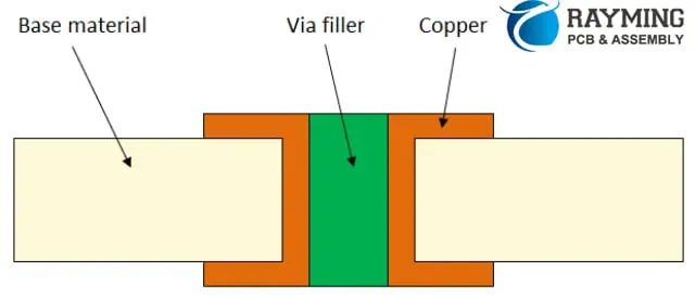
The global electroplating PCB industry’s output value accounts for a rapid increase in the proportion of the total output value of the electronic components industry. It is the industry with the largest proportion of the electronic component segmentation industry, and has a unique position. The annual output value of electroplated PCB is 60 billion US dollars. The volume of electronic products is becoming thinner and lighter, and direct stacking on blind vias is a design method for obtaining high-density interconnects. To make a stack of holes, you should first do a good job at the bottom of the hole. There are several methods for fabricating a typical flat hole surface, and a plating hole filling process is one of them.
https://www.youtube.com/watch?v=c_QpC91z_do
In addition to reducing the need for additional process development, the electroplating and hole-filling process is also compatible with current process equipment, which is beneficial for good reliability.
Electroplating and filling holes have the following advantages:
(1) It is advantageous to design stacked and on-disk holes (Via.on.Pad);
(2) Improve electrical performance and contribute to high frequency design;
(3) Helps to dissipate heat;
(4) The plug hole and the electrical interconnection are completed in one step;
(5) The blind holes are filled with electroplated copper, which has higher reliability and better conductivity than conductive paste.
Physical influence parameter:
The physical parameters that need to be studied are: anode type, anode-anode spacing, current density, agitation, temperature, rectifier, and waveform.
(1)Type of anode. When it comes to anode type, it is nothing more than a soluble anode and an insoluble anode. The soluble anode is usually a phosphorus-containing copper ball, which easily produces anode mud, contaminates the plating solution, and affects the performance of the plating solution. Insoluble anodes, also known as inert anodes, are typically composed of a titanium mesh coated with a mixed oxide of cerium and zirconium. Insoluble anode, good stability, no anode maintenance, no anode mud generation, pulse or DC plating are applicable; however, the additive consumption is large.
(2)The anode-anode spacing. The design of the spacing between the cathode and the anode in the electroplating process is very important, and the design of different types of equipment is not the same. However, it should be pointed out that no matter how the design is, it should not violate the first law of Farah.
(3)Stirring. There are many types of mixing, such as mechanical rocking, electric shock, gas vibration, air agitation, and jet (Eductor).
For electroplating and filling holes, it is generally preferred to increase the jet design in the configuration of conventional copper cylinders. However, whether it is the bottom jet or the side jet, how is the jet pipe and the air agitating pipe arranged in the cylinder; what is the jet flow per hour; how much the jet pipe is spaced from the cathode; if the side jet is used, the jet is at the anode Whether the front or the back; if the bottom jet is used, will it cause uneven mixing, the plating solution is weak and strong; the number, spacing and angle of the jet on the jet tube are factors that must be considered in the design of the copper cylinder, and also A lot of trials are going on.
In addition, the most ideal way is to connect each flow tube to the flowmeter to achieve the purpose of monitoring the flow. Temperature control is also important because the flow rate is large and the solution is prone to heat.
(4)Current density and temperature. Low current density and low temperature can reduce the deposition rate of surface copper while providing sufficient Cu2 and brightener into the pores. Under these conditions, the ability to fill holes is enhanced, but at the same time the plating efficiency is also reduced.
(5) Rectifier. The rectifier is an important part of the electroplating process. At present, the research on electroplating and filling holes is mostly limited to full-plate electroplating. If the pattern plating hole is considered, the cathode area will become small. At this time, high requirements are placed on the output accuracy of the rectifier.
The output accuracy of the rectifier should be chosen according to the line of the product and the size of the via. The finer the lines and the smaller the holes, the higher the accuracy requirements for the rectifier. Generally, a rectifier with an output accuracy of 5% or less should be selected. Exceeding the accuracy of the selected rectifier will increase the investment in the equipment. For the output cable of the rectifier, the rectifier should be placed on the side of the plating tank as much as possible. This can reduce the length of the output cable and reduce the pulse current rise time. The rectifier output cable specification should be chosen to meet the line drop of the output cable within 0.6V at 80% of the maximum output current. The required cable cross-sectional area is usually calculated at a current carrying capacity of 2.5 A/mm:. If the cross-sectional area of the cable is too small or the cable length is too long and the line voltage drop is too large, the current will not reach the current value required for production.
For plating tanks with a groove width greater than 1.6 m, bilateral input should be considered and the length of the bilateral cables should be equal. In this way, it is guaranteed that the bilateral current error is controlled within a certain range. A rectifier should be connected to each side of each fly-bar of the plating tank so that the currents on both sides of the part can be adjusted separately.
(6)At present, from the perspective of waveforms, there are two types of electroplating holes: pulse plating and DC plating. These two methods of electroplating and filling have been studied. The DC electroplating hole is made of a conventional rectifier, which is easy to operate, but if the plate is thick, it is powerless. The pulse plating filling hole adopts the PPR rectifier, and the operation steps are many, but the processing ability for the thicker plate is strong.
Substrate influence
The influence of the substrate on the electroplating and filling holes is also negligible. Generally, there are factors such as dielectric layer material, hole shape, aspect ratio, and chemical copper plating.
(1) Dielectric layer material. The dielectric layer material has an effect on the filling of holes. Non-glass reinforced materials are easier to fill than holes in glass reinforced materials. It is worth noting that the glass fiber protrusions in the holes have an adverse effect on the chemical copper. In this case, the difficulty in electroplating is to increase the adhesion of the electroless plating seed layer, rather than the hole filling process itself.
In fact, electroplating and filling holes on glass fiber reinforced substrates have been used in actual production.
(2)Thickness to diameter ratio. At present, the hole-filling technology for different shapes and different sizes of holes is highly valued by both manufacturers and developers. The hole filling ability is greatly affected by the hole thickness ratio. Relatively speaking, DC systems are more widely used commercially. In production, the size of the hole will be narrower, generally 80pm ~ 120Bm diameter, hole depth 40Bm ~ 8OBm, thickness to diameter ratio does not exceed 1:1.
(3) Electroless copper plating. The thickness and uniformity of the chemical copper plating and the placement time after electroless copper plating all affect the hole filling performance. Chemical copper is too thin or uneven in thickness, and its hole filling effect is poor. Generally, it is recommended to fill holes when the thickness of the chemical copper is >0.3 pm. In addition, the oxidation of chemical copper also has a negative effect on the hole filling effect.
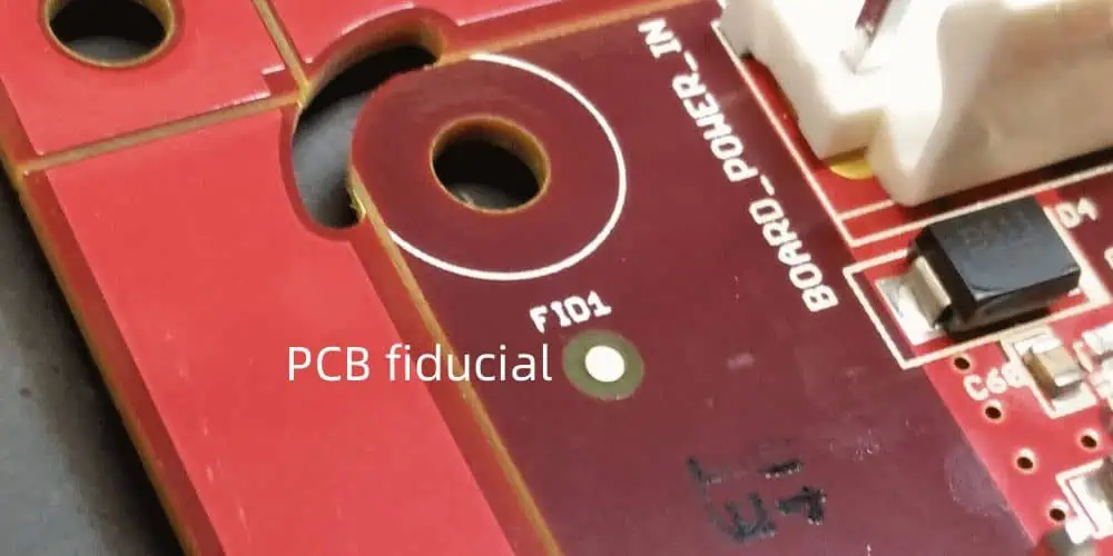
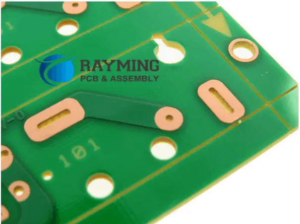
In PCB design, a fiducial marker is a small, rounded copper feature that serves as a reference point for automated pick-and-place assembly machines. These markers enable machine vision systems to accurately detect the PCB’s position and orientation as it moves through Surface Mount Technology (SMT) assembly lines. By comparing the PCB’s alignment with the pre-programmed orientation of components on reels, the machine can adjust part placement—including rotation—to ensure precise positioning on their designated land patterns.
Why Use Fiducial Markers?
Fiducials are a simple yet critical feature that should be incorporated into PCB designs whenever possible, particularly for square or rectangular boards. They enhance assembly accuracy and reduce misalignment errors, which is especially important for:
High-density designs (e.g., fine-pitch components like QFPs, BGAs, or QFNs)
High-volume production (where consistency is crucial)
Placement Guidelines
Global Fiducials – Typically placed near the PCB corners to provide overall board alignment.
Local Fiducials – Positioned near critical components (e.g., fine-pitch ICs) to improve placement precision for specific parts.
The choice between global and local fiducials depends on:
Component pitch (smaller pitches often require additional fiducials for accuracy)
Production volume (high-volume runs benefit from both types)
Assembler requirements (some may demand local fiducials for tight-tolerance components)
Fiducial markers are essential reference points in PCB manufacturing that enable precise component placement during automated assembly. These copper landmarks guide pick-and-place machines by providing exact positional data, ensuring accurate alignment of surface-mount components.
Two Key Types of Fiducial Markers
Global Fiducial Markers
Positioned near the PCB edges to establish the board’s overall orientation.
Help machines determine the PCB’s X-Y axis alignment and correct for any skew or misplacement when clamped.
Critical for ensuring panel-level accuracy in high-volume production.
Local Fiducial Markers
Placed adjacent to high-precision components, such as quad flat packages (QFPs), BGAs, or fine-pitch ICs.
Provide component-specific alignment, minimizing placement errors for sensitive parts.
Particularly vital for:
Fine-pitch components (≤0.5mm lead spacing)
Large ICs requiring exact positioning (e.g., processors, FPGAs)
Why Are Fiducial Markers Crucial?
Improve Placement Accuracy: Prevent misalignment in automated SMT assembly.
Reduce Defects: Minimize soldering errors and tombstoning.
Support High-Density Designs: Essential for modern PCBs with micro-BGAs and ultra-fine-pitch components.
By strategically using global and local fiducials, manufacturers can achieve higher yields, lower rework costs, and more reliable PCB assemblies.
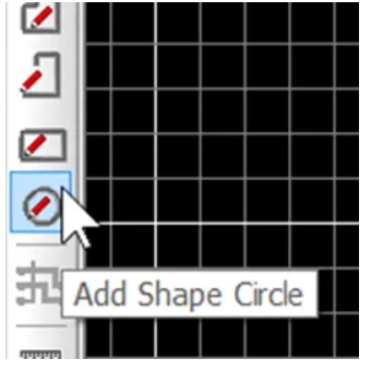
The use of the “Add Shape Circle” provides the required flexibility for this.
When creating a fiducial marker, proper grid configuration ensures accurate alignment and simplifies the design process. For a standard 1mm copper pad with a 3mm solder mask opening, follow these steps:
Set Your Design Grid to 1mm
This establishes a consistent reference scale for precise element placement.
Enable Snap-to-Grid at 0.25mm or 0.5mm Increments
Allows finer control when positioning the fiducial while maintaining alignment to the primary grid.
Ensures perfect centering of the copper pad within the solder mask aperture.
Implementation Benefits
Guaranteed concentricity between copper and mask layers
Efficient editing with automatic alignment to design rules
Manufacturing-friendly output that avoids tolerance stacking issues
Pro Tip: For high-density designs, combine this approach with a 45° rotated grid when placing diagonal fiducial arrays to maintain optical recognition reliability.
This methodology is particularly valuable when working with:
Using this structured approach eliminates guesswork and ensures your fiducials meet IPC-7351 standards for machine vision recognition.
Key Advantages:
Precision: Maintains perfect geometric relationships between layers
Efficiency: Reduces design time with intelligent snapping
Reliability: Produces manufacturing-ready fiducials in 3 quick steps
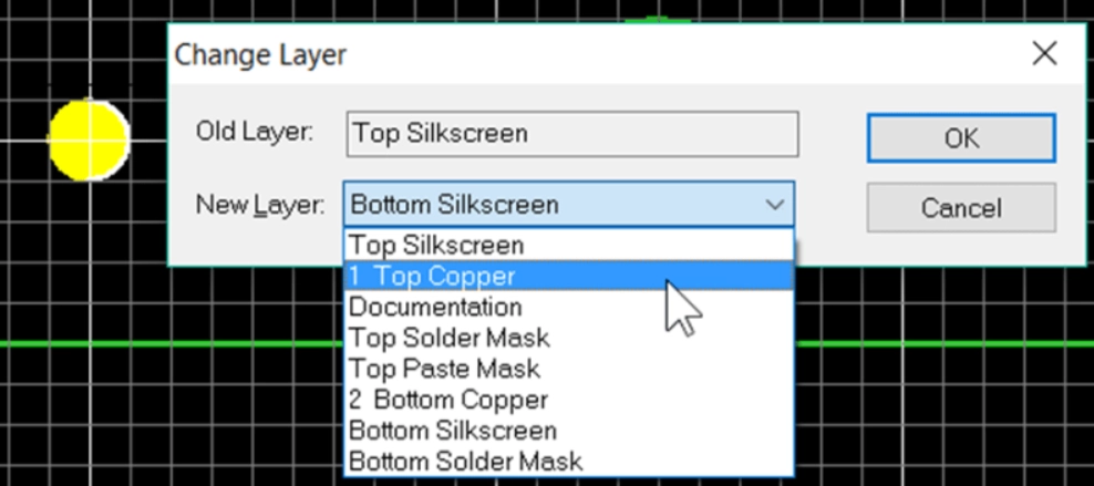
Select the “Add Shape Circle” and right-click before placing and ensure “Filled Shape” is set, you may also select the Layer or change layers after placing as shown.
Place the circle shape and expand to the next half-grid line. Note grid setting in this example are 0.5mm.
If required then change the layer using the “L” key shortcut or select the object, right-click and select “Layers”. Change the layer to Top Copper.
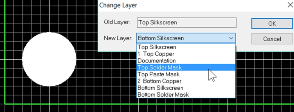
Repeat for solder mask exclusion area by adding another closed circle shape over the copper shape and change the layer to Top Solder Mask. The solder mask is a negative image, the shape will correspond to the excluded area of solder resist.
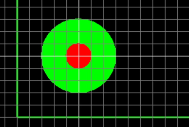
The fiducial is now created, use F5 to redraw the view.
At this point it is good practice to select the fiducial, right click and select ‘Group’, this will prevent the copper circle and solder mask from becoming misaligned.
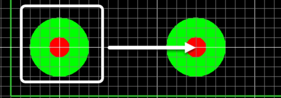
Further fiducials can be simply placed by selecting the fiducial and copying by CTRL+C and pasting by CTRL+V.
Although the fiducial cannot be saved as a library component a quick and easy solution for future use is to save the fiducial as a PCB design with the fiducial. When working on a new design also open this PCB design and you can copy and paste the fiducial to your current design as shown below.
PCB Fiducial Design Guidelines: Essential Rules for Machine Vision Accuracy
Fiducial markers require careful design to ensure reliable detection by assembly equipment. Follow these critical guidelines to optimize fiducial performance in your PCB layout.
1. Keep-Out Area Requirements
Minimum Clearance Radius: At least 2× the fiducial diameter (per SMEMA 3.1)
Example: A 1mm fiducial needs a 2mm clearance radius from copper traces/pours.
Concentric Alignment: Fiducial and keep-out zones must share the same center point.
Edge Clearance: Maintain >4.75mm (187 mils) from board edges to avoid pick-and-place clamp interference.
Why?
Nearby copper or traces can reduce contrast, confusing machine vision.
Clamps covering fiducials lead to assembly misalignment.
2. Fiducial Size & Consistency
Diameter Range:1.00mm (40 mils) to 3.00mm (118 mils) (SMEMA standard).
Size Matching: Fiducials must match within ±25µm (1 mil) across the PCB.
Best Practice: Reuse the same fiducial padstack from your library to ensure uniformity.
3. Surface Finish & Protection
Avoid Bare Copper: Oxidized/tarnished copper reduces optical contrast.
Recommended Finishes:
ENIG (Electroless Nickel Immersion Gold) – Best for long-term reliability.
HASL (Hot Air Solder Leveling) – 5–10µm thickness (max 25µm).
Solder Mask:
Must be opened over the fiducial (no coverage).
Glossy solder mask can cause reflections, interfering with machine vision.
4. Placement & Design Considerations
Location: Typically placed in corners (global fiducials) or near high-precision components (local fiducials).
Internal Layers: Suppress fiducial pads on non-essential layers (e.g., no inner-layer pads needed).
Copper Pours: Allowed beneath fiducials (no electrical impact).
5. Best Practices for Manufacturing (DFM)
✅ Verify fiducial consistency in final design reviews. ✅ Use plated finishes (ENIG/HASL) to prevent oxidation. ✅ Avoid solder mask coverage—ensure proper mask opening. ✅ Check edge clearance to prevent clamp obstruction.
By following these rules, you ensure high assembly accuracy, fewer defects, and smoother automated production.
On printed circuit boards, the surface finish applied to the exposed copper traces and pads is a critical parameter impacting solderability, shelf life, and assembly performance.
One surface finish option is OSP – Organic Solderability Preservative. In this article, we’ll provide a comprehensive overview of PCB OSP coating covering:
What OSP is and how it is applied
Benefits and downsides compared to other finishes
How OSP protects copper from oxidation
Impact on soldering and solderability
Shelf life and storage considerations
Uses and applications where OSP makes sense
How to specify OSP on fabrication drawings
FAQs about OSP use and capabilities
After reading this guide, you’ll understand what the OSP surface finish is, where it shines, and how to effectively leverage it on your PCBs. Let’s get started!
OSP stands for Organic Solderability Preservative. As the name indicates, it is an organic coating applied to the copper traces of a PCB to protect them from oxidation and maintain solderability.
The OSP finish contains an organic acid that reacts with the copper surface to form a protective layer only a few atoms thick. This prevents air from reaching the copper and oxidizing it.
Key properties of OSP include:
Thin organic coating measured in angstroms
Applied through an aqueous chemistry process
Prevents copper oxidation for a fixed shelf life
Provides good wetting and solderability
Lower cost than many other finishes
Environmentally friendly process
With its ability to protect copper, maintain solderability, and low cost, OSP offers some major benefits but also must be applied judiciously based on design needs.
Benefits of OSP Finish
Here are some of the major advantages of using an OSP surface finish on PCBs:
Solderability
Preserves good wetting and solderability of copper traces
Allows soldering after months of shelf life
Lower Cost
OSP chemistry is low cost compared to many finishes
Process does not require significant equipment investment
Environmental Friendliness
Aqueous process with minimal chemical waste
Easy rinsing and lower toxicity effluents
Repairability
Unlike some finishes, OSP allows rework and repair of solder joints
With tighter process controls, these limitations can be managed. But they do require awareness when applying OSP.
How OSP Protects Copper from Oxidation
The OSP organic compound reacts with the top few atomic layers of copper to form a protective coating of copper-OSP complexes.
This thin barrier prevents oxygen and humidity from reaching the copper traces underneath. So the copper is preserved from oxidizing and remains solderable.
However, over time the protection diminishes as the OSP gradually gets consumed through:
Exposure to atmosphere
Traces rubbing and abrading
Thermal cycling and reflow depleting the OSP layer
OSP shelf life until oxidation occurs depends on coating thickness and storage conditions. But expect 6-12 months maximum before issues arise.
OSP Impact on Soldering and Solderability
A key benefit of OSP is maintaining good solderability of the copper pads and traces. This allows successful hand and reflow soldering.
The thin OSP coating does not function as a thermal barrier during soldering. The organic acids vaporize locally as the pad heats up, exposing the fresh copper underneath to melt and alloy with the solder.
However, each soldering process does consume a bit of the OSP thickness. So solderability degrades after repeated reflows as the copper begins showing through.
OSP lasts through around 4-6 reflow cycles typically. For boards that undergo lots of rework, OSP may not be the optimal finish choice.
Shelf Life and Storage Considerations
Since OSP only protects copper for a limited time, proper storage is critical. Here are some guidelines:
Store in low humidity environment < 30% RH
Use moisture barrier bags and desiccant packs
Avoid direct sunlight exposure
Control storage temperature stable around 20°C
First-in-first-out (FIFO) inventory management
Test solderability if stored over 6 months
With careful moisture control and storage tenure tracking, OSP coated boards can last 9-12 months before substantial oxidation appears.
Long term storage or harsh conditions shorten usable life. But good controls allow tapping the benefits of OSP when appropriate.
Uses and Applications Suited for OSP
Here are some typical uses and applications where OSP is a strong surface finish choice:
Low Volume Prototypes
Provides solderability for prototype runs
Avoids higher cost finishes for short runs
Double-Sided Boards
Good match to lower complexity boards
Reduces cost versus immersion finishes
Quick-Turn Fabrication
Fast application suits quick turns around
Automated Assembly
Solderability survives pick-and-place
Finish withstands conveyor handling
Manual Soldering
Maintains pad solderability for hand assembly
Lower cost than noble metal finishes
Engineering Testing
Allows functional board testing before production
Avoids cost of final finish for eval boards
Short Shelf Life Designs
Acceptable if product ships quickly
Mitigates the short OSP lifespan
How to Specify OSP on Fabrication Drawings
Here are some tips for effectively specifying OSP finish on fabrication documentation:
Call out OSP finish for the appropriate trace layers
Indicate maximum allowed shelf life e.g. 9 months
Define expected storage conditions if high humidity
Specify maximum reflow cycles e.g. 4 passes
Require solderability testing after certain duration
A: Yes, OSP processes are designed to be lead-free and conform to RoHS guidelines.
Q: Can components be mixed on boards with OSP and ENIG finishes?
A: Generally this is okay but beware ENIG may outlast OSP and require matching lifecycles.
Q: Can OSP withstand multiple reflow cycles?
A: OSP can survive around 4-6 reflows before pads oxidize. So minimize rework.
Q: What checks ensure an effective OSP coating?
A: Suppliers should test thickness, solderability after thermal shock, and other parameters per IPC specs.
Q: Does OSP have to be removed for hot air solder leveling?
A: No, OSP can remain during HASL application and enhances solderability.
Conclusion
In summary, OSP finish provides a lower cost solderable coating for PCBs when properly applied. It excellently protects copper traces from oxidation for months when well controlled.
However, OSP does have shelf life limitations and diminishes after multiple reflows. This requires matching OSP to appropriate short shelf life or low assembly complexity designs.
With its environmental friendliness, cost savings, and ease of application, OSP strikes an excellent balance for many less demanding uses. Just be aware of the tradeoffs versus more robust finishes.
Collaborating with your PCB manufacturer to apply OSP selectively based on design needs ensures gaining maximum benefit from this useful surface finish where it fits best.
In the making process of printed circuit boards the surface of the board is coated with copper. All electric connections depend upon the conductivity of the copper. On the other hand, the copper is also highly chemically reactive, when it exposed to the moisture of atmosphere it oxidizes abruptly. As a result high temperature requirement for soldering and ultimately it affect the end product reliability. Therefore there is need aroused for surface finishing of boards. The employment of surface finish coating serve two purposes, the first is to protect copper from oxidizing and another is to provide a surface which can maintain it quality after soldering and during assembly of various components with printed circuit boards.
There are various types of surface finishes available which involves various chemical substances, like: Hot air soldering leveling, Immersion in Tin/silver, OSP and ENIG. Among all these processes of surface finishing OSP has turned out to be a low cost process and environment friendly.
Introduction: OSP abbreviated as “Organic Solderability Preservative” . At the time of surface finishing of board it refers to a organic layer, which adhere with the copper by means of adsorption. Being organic it is permanent wall to prevent oxidation of copper, thermal shocks moisture. This organic coating also gives easy removal or less deposition of flux during soldering and ultimately helps to reduce the soldering time of assembly process of printed circuit board.
The chemical compound associated with this process belong to azole family compounds like benzotriazoles, imidazoles and benzimidazoles. All these chemicals by means of coordination bonding adsorbed on the copper surface, and a film is created over the entire board. The thickness of surface finish coating depends upon what chemical compound is used to proceed. For example the film made through benzotriazeoles is thin, on the contrary that through imidazoles are thick. Therefore according to requirement the chemical compound is being selected for surface finishing.
In this process topographical enhancement are also implemented. Microetching usually eliminates the oxidation of copper and also strengthens the bonds between copper and the pcb OSP solution. The speed of micro etching is also an important parameter for surface finishing. Usually the speed of etching is 1 to 1.5µm per minute.
Advantages of OSP
The major point is the low cost and easy processing makes this process of surface finishing more popular across the printed circuit board industry. Few advantages are enlisted below:
1. Simple PCB Manufacturing process: Printed circuit boards coated with OSP are easy to rework and maintain. Therefore, it is an advantage for PCB manufacturers to repair the surface finish coating with less time and cost, once coating found damaged.
2. OSP coated boards gives good performance in terms of solder wetting and joining between flux, vias and pads.
3. Because of application of water based compound in OSP surface finishing, makes it environment friendly. Therefore this can be termed as a green electronic product which is catering to the green regulations.
4. Implementation of simple chemical compound and less complexity of process it is of low cost. With most of the chemicals of OSP there is no need of solder mask ink. But some chemicals require a little proportion of solder mask ink in some special cases.
5. Storage time is long for the printed circuit board if coated with OSP. It is implemented with single-side SMT assembly as well as double sided prototype pcb assembly.
Storage Requirement: The coating generated by OSP surface finish is quite thin. Therefore, care must be taken, when printed circuit in operation or is being transported. If board with OSP surface finish is exposed to the open atmosphere and humidity, then there are chances that oxidation will possibly damage the surface of printed circuit board, and then it leads to further consequences ahead in the process of assembly and its functioning. There are certain principle which are required to be followed during storage and transportation of OSP finished printed circuit board:
1. Vacuum packaging could be a solution. Also there is a requirement to save the printed circuit board from friction. In order to achieve that a release paper must be provided between boards. Since the assembly is very delicate, then minor negligence would affect the cost and other parts.
2. OSP surface finished printed circuit boards are not directly exposed to sunlight. The standard storage requirement for boards as such: relative humidity(30-60%RH), temperature (15to28oC)and storage time must be less than 12 hours.
In some cases the OSP surface finishing changes its color when various electronic components are assembled with the printed circuit board. This ultimately affect the thickness of the preservative over the board surface, micro etching quantity, enhanced soldering time and dispersion of unwanted particles over the board surface. This problem can be inspected visually.
There are two possibility:
1. In the process of soldering , flux is capable enough to eliminate oxidation of the coating. Then it cannot influence the soldering performance. Therefore, there are no such measures required for prevention.
2. Because of inability of flux the oxidation of the surface finish coating takes place, and this ultimately result decline in soldering performance.
Therefore, following measures can be taken to ensure the performance and appearance of OSP surface finish in the printed circuit board manufacturing process.
3. Thickness of the OSP layer is very critical. Therefore, it is require to keep it in a specified range.
4. Similarly amount of micro etching also required to be controlled within the standard range.
5. During the fabrication process of printed circuit board, it must be taken into consideration that no residual deposits remain over the OSP coating. If such residual deposited over the board then it affect the performance of soldering ability.
In today’s rapidly evolving electronics industry, the quality of printed circuit boards (PCBs) is paramount. As the backbone of electronic devices, PCBs demand rigorous inspection processes to ensure functionality, reliability, and longevity. This article delves into the critical aspects of PCB quality inspection and provides actionable strategies to enhance your inspection procedures.
Introduction
Quality inspection of PCBs is not just a final checkpoint; it’s a crucial process that permeates every stage of PCB manufacturing. The consequences of poor PCB inspection can be severe, ranging from product failures and costly recalls to irreparable damage to a company’s reputation. By focusing on defect detection, reliability assurance, and continuous process improvement, manufacturers can significantly elevate their PCB quality standards.
1. Understanding the Types of PCB Defects
To improve PCB quality inspection, it’s essential to have a comprehensive understanding of the various defects that can occur during the manufacturing process.
Common PCB Defects
Open Circuits: Breaks in the conductive paths that prevent electrical flow.
Short Circuits: Unintended connections between two or more circuit elements.
Solder Bridges: Excess solder forming unwanted connections between pads or tracks.
Component Misalignment: Incorrect positioning of components on the board.
Delamination: Separation of the PCB layers due to heat or moisture.
Copper Traces Issues: Including under-etching, over-etching, or mouse bites.
Via Defects: Such as blocked vias or insufficient plating.
Classification of Defects
PCB defects can be broadly classified into two categories:
Visual Defects: These are issues that can be detected through visual inspection, such as misaligned components, solder bridges, or physical damage to the board.
Electrical Defects: These defects affect the electrical performance of the PCB and may not be visible to the naked eye. Examples include open circuits, short circuits, and impedance issues.
Importance of Root Cause Analysis
Understanding the root causes of defects is crucial for long-term quality improvement. By identifying patterns and common sources of defects, manufacturers can implement preventive measures and refine their processes. Root cause analysis should be an integral part of the quality inspection workflow, involving cross-functional teams from design, manufacturing, and quality assurance.
Consistency in quality inspection is key to maintaining high standards across production runs. Standardizing inspection criteria provides a clear benchmark for quality and helps in training inspectors effectively.
Importance of Clear Quality Standards
Industry-recognized standards such as IPC-A-600 (Acceptability of Printed Boards) and IPC-A-610 (Acceptability of Electronic Assemblies) provide comprehensive guidelines for PCB quality. These standards cover various aspects of PCB manufacturing and assembly, including:
Adhering to these standards ensures that your PCBs meet industry-accepted quality levels and facilitates communication with customers and suppliers.
Customizing Standards for Specific Requirements
While industry standards provide an excellent baseline, many products require additional or more stringent criteria. Customizing inspection standards based on specific product requirements is essential, especially for high-reliability applications such as medical devices, aerospace, or automotive electronics.
Consider the following when customizing standards:
Environmental conditions the PCB will face (temperature, humidity, vibration)
Expected lifespan of the product
Regulatory requirements specific to the industry
Customer specifications and expectations
Documenting Inspection Protocols and Defect Tolerances
Clear documentation of inspection protocols and defect tolerances is crucial for consistent quality control. This documentation should include:
Detailed inspection procedures for each stage of production
Acceptable limits for various types of defects
Decision trees for classifying and handling defects
Guidelines for when to reject a board or batch
Procedures for reporting and escalating quality issues
Regularly review and update these documents to reflect process improvements and changes in product requirements.
3. Investing in the Right Inspection Methods
Choosing the appropriate inspection methods is crucial for effective quality control. Each method has its strengths and is suited to different stages of the production process.
Manual Visual Inspection (MVI)
Pros and Cons
Pros:
Low initial investment
Flexibility to adapt to different products
Ability to detect subtle defects that automated systems might miss
Cons:
Prone to human error and fatigue
Inconsistent results between inspectors
Time-consuming for high-volume production
Best Practices to Reduce Human Error
Implement regular breaks to combat fatigue
Use magnification tools and proper lighting
Rotate inspectors between different tasks
Conduct regular refresher training
Automated Optical Inspection (AOI)
How AOI Systems Work
AOI systems use high-resolution cameras and sophisticated image processing algorithms to detect visual defects. They compare the captured images of PCBs against a “golden” reference to identify anomalies.
When to Implement AOI
For high-volume production where speed is essential
When dealing with complex, densely populated boards
To ensure consistency in inspection quality
As a complement to manual inspection for critical areas
Automated X-ray Inspection (AXI)
X-ray inspection is invaluable for detecting hidden defects, particularly in multi-layer boards and for inspecting solder joints under components like Ball Grid Arrays (BGAs).
Use Cases for AXI
Inspecting solder joints in BGAs, QFNs, and other hidden connections
Detecting voids in solder joints
Checking internal layers of multi-layer PCBs
Identifying counterfeit components
Flying Probe Testing / In-Circuit Testing (ICT)
These methods test the electrical functionality of PCBs, complementing visual inspection techniques.
Flying Probe Testing
Ideal for low to medium volume production
Flexible and requires minimal fixture costs
Can test both assembled and bare boards
In-Circuit Testing (ICT)
Suited for high-volume production
Requires custom fixtures but offers faster test times
Provides comprehensive electrical testing of components and connections
Functional Testing
As the final stage of validation, functional testing ensures that the PCB performs as intended in its actual application environment.
Key Aspects of Functional Testing
Simulates real-world operating conditions
Verifies overall functionality and performance
Identifies issues that may not be apparent through other inspection methods
4. Improving Inspector Training and Certification
The quality of inspection is directly related to the skill and knowledge of the inspectors. Investing in comprehensive training and certification programs is essential for maintaining high standards.
Regular Training Programs
Conduct periodic training on new defect types and emerging technologies
Use real-world examples and case studies to enhance learning
Implement hands-on training with a variety of PCB types and defects
Emphasis on Attention to Detail and Pattern Recognition
Develop exercises to improve visual acuity and pattern recognition skills
Train inspectors to recognize subtle variations that may indicate defects
Encourage a methodical approach to inspection to ensure thoroughness
Certification Programs
Implement industry-recognized certifications such as IPC-A-610 Certified IPC Specialist
Develop in-house certification programs tailored to your specific products and processes
Regularly assess and recertify inspectors to ensure skills remain current
5. Optimizing Inspection Process Flow
Efficient organization of the inspection process can significantly impact overall quality and productivity.
Inline vs. Offline Inspection
Inline Inspection
Integrates inspection directly into the production line
Provides immediate feedback and reduces handling
Ideal for high-volume production with consistent product types
Offline Inspection
Allows for more detailed inspection without impacting line speed
Suitable for complex boards or when additional time is needed for thorough checks
Can be used for random sampling or as a secondary inspection step
Strategic Placement of Inspections
Implement a multi-stage inspection strategy:
Pre-solder Inspection: Check component placement and board condition before soldering
Post-solder Inspection: Verify solder joint quality and component alignment after soldering
Final Inspection: Comprehensive check of the assembled PCB before functional testing
Using Sampling Plans Effectively
For high-volume production, 100% inspection may not be feasible. Implement statistical sampling plans:
Use AQL (Acceptable Quality Limit) standards to determine sample sizes
Implement tightened, normal, and reduced inspection levels based on historical quality data
Adjust sampling frequency based on the criticality of the product and process stability
6. Using Data-Driven Quality Control
Leveraging data analytics can provide valuable insights for continuous improvement of PCB quality.
Defect Tracking Systems and Software
Implement robust defect tracking software to log and categorize all identified issues
Use barcode or RFID systems to track individual boards through the inspection process
Generate real-time reports on defect rates and types
Statistical Process Control (SPC) and Trend Analysis
Use SPC charts to monitor key quality indicators over time
Identify trends and patterns in defect occurrences
Set control limits and implement corrective actions when processes deviate
Root Cause and Corrective Action (RCCA) Feedback Loops
Establish a formal RCCA process for addressing recurring quality issues
Involve cross-functional teams in problem-solving sessions
Document and share lessons learned to prevent future occurrences
7. Continuous Improvement and Innovation
Quality inspection should be viewed as an evolving process, constantly adapting to new challenges and technologies.
Implementing Lessons Learned
Regularly review inspection data and customer feedback to identify areas for improvement
Update inspection criteria and processes based on new insights
Share best practices across different production lines and facilities
Regular Process Audits and Supplier Inspections
Conduct periodic audits of your inspection processes to ensure adherence to standards
Extend quality requirements to suppliers and perform regular supplier audits
Collaborate with suppliers to improve incoming material quality
Exploring AI and Machine Learning for Predictive Quality Inspection
Investigate AI-powered defect detection systems for more accurate and faster inspections
Use machine learning algorithms to predict potential quality issues based on historical data
Implement predictive maintenance for inspection equipment to minimize downtime
8. Collaboration Between Design and Manufacturing Teams
Effective PCB quality inspection starts at the design stage. Fostering collaboration between design and manufacturing teams can preemptively address many quality issues.
Importance of Design for Manufacturability (DFM) Reviews
Conduct regular DFM reviews to identify potential manufacturing challenges early
Use DFM software tools to analyze designs for compliance with manufacturing capabilities
Establish clear communication channels between design and manufacturing teams
Early Detection of Design Issues
Implement simulation tools to predict potential defects or reliability issues
Create prototypes or use 3D printing to validate designs before full production
Encourage feedback from manufacturing and quality teams during the design phase
Conclusion
Improving PCB quality inspection is a multifaceted endeavor that requires a holistic approach. By understanding defect types, standardizing criteria, investing in appropriate inspection methods, and fostering a culture of continuous improvement, manufacturers can significantly enhance their PCB quality.
Remember that rigorous PCB inspection is not just about catching defects; it’s about driving overall quality improvement throughout the entire manufacturing process. By treating inspection as an integral part of your quality management system rather than a final checkpoint, you can achieve higher reliability, reduce costs, and ultimately deliver superior products to your customers.
As technology continues to evolve, so too must PCB inspection methods. Stay informed about emerging technologies and industry trends, and be prepared to adapt your inspection processes accordingly. With a commitment to excellence and a data-driven approach to quality, you can position your PCB manufacturing operation at the forefront of the industry, ready to meet the challenges of tomorrow’s electronic devices.
PCB copper plating refers to the process of electroplating a thin layer of copper onto a printed circuit board (PCB) substrate. The copper layer serves as the conductive pathways or traces for the electrical current to flow.
Copper is the metal of choice for PCB fabrication for several reasons:
Excellent electrical conductivity. Copper has a very low resistivity, allowing current to flow efficiently.
Corrosion resistance. Copper forms a protective patina when exposed to air that prevents further corrosion.
Solderability. Copper readily forms intermetallic compounds with solder, creating strong solder joints.
Cost. Copper is affordable compared to other conductive metals like gold or silver.
The copper thickness on a PCB can vary depending on the current flow requirements. Still, typical copper weights (thickness) are 1 oz (35 μm) and 2 oz (70 μm) for outer layers and 0.5 oz (17 μm) for inner layers.
Plating refers to the electrochemical process of depositing a metal coating onto a conductive surface. To electroplate copper onto a PCB substrate, the board is immersed in a copper electrolyte solution and electrically charged to attract copper ions onto its surface.
So in summary, PCB copper plating is the process of electroplating a copper film onto a PCB substrate to create the conductive traces or circuitry. Proper plating thickness and quality are essential for a functioning high-reliability PCB.
There are several key reasons why copper is the preferred metal used for plating PCBs:
1. Excellent Electrical Conductivity
Copper has the highest electrical conductivity rating among commercial metals. With a conductivity of 5.96×10⁷ S/m, copper allows electrical current to flow with little resistance. This enables PCBs to operate at higher frequencies and speeds.
2. Corrosion Resistance
Copper forms a patina oxide layer when exposed to oxygen that protects it from further corrosion. This property allows copper traces to withstand oxidation and endure long-term use in electronics.
3. Solderability
Copper readily alloys with tin-lead solder to form high-strength solder joints. The intermetallic compounds create an excellent bonding interface between copper PCB traces and component leads.
4. Thermal Conductivity
Copper has excellent thermal conductivity, allowing it to dissipate heat efficiently from high power PCB components. This helps avoid excessive thermal buildup and component failure.
5. Ductility
Copper is highly ductile, allowing it to be rolled or pressed into thin sheets or foils. This thin foil can be laminated onto PCB substrates.
6. Cost
Copper is much more affordable compared to other highly conductive metals like gold, silver, or palladium. This lower cost makes it commercially viable for all types of PCB manufacturing.
In summary, copper’s blend of electrical and thermal conductivity, corrosion resistance, ductility, and cost-effectiveness make it universally adopted as the conductor of choice for PCB plating.
PCB Copper Plating Methods
There are several techniques used in the PCB fabrication industry to deposit copper onto substrates. The most common plating methods include:
Electroless Copper Plating
Electroless copper plating is an auto-catalytic process used to deposit an initial thin copper layer onto non-conductive surfaces. It does not require any external power source. The PCB substrate is immersed in a copper solution which plates copper onto the board through a chemical reducing reaction.
Electroless copper allows plating on dielectric materials like FR-4, Flex, ceramics etc. It provides an initial conductive layer which allows subsequent electrolytic plating. The thickness of electroless copper is typically 0.1-0.5 μm.
Electrolytic Copper Plating
Electrolytic plating requires the substrate to be electrically conductive. It uses electrical current to deposit copper ions onto the PCB from a copper electrolyte solution. Electrolytic plating forms the bulk of copper thickness on a PCB due to its faster deposition rate.
Thickness can be precisely controlled by adjusting the electrical current and plating time. High electrical current densities allow thickness of up to 70 μm to be achieved. PCB panels are plated using either vertical plating or horizontal plating processes.
Panel Plating
In panel plating, the PCB substrate panels are arranged vertically in a plating tank with the copper anode plates. The parallel arrangement allows higher current densities resulting in faster plating. Vertical panel plating is ideal for high-volume PCB production.
Pattern Plating
This method selectively deposits copper only onto the circuit regions on a panel. A photoresist dry film is laminated and imaged to expose only the desired copper pattern. This allows plating copper traces directly without any etching. It eliminates copper waste and is a cleaner process.
Through-Hole Plating
Boards with plated through-holes require copper to be plated onto the inner walls of the drilled holes. This electrically connects the conducting layers to allow current flow between layers. Electroless copper first seeds the hole walls, followed by electrolytic copper plating to build up thickness.
PCB Copper Plating Process Steps
PCB pattern plating line
The typical sequence of PCB copper plating steps is as follows:
Drilling – Through-holes are mechanically drilled as per circuit design. Panels may also be slotted or routed if required.
Deburring – The holes are deburred using abrasive media to remove rough edges and drill debris.
Cleaning – Alkaline cleaners remove drilling oils, resins, and debris from the panels.
Activation – Panels are microetched and treated with a predip chemical to remove oxides and activate surfaces.
Electroless Copper – An initial thin layer of electroless copper is deposited on non-conducting substrate.
Panel Dry Film – A photoresist dry film laminate is applied on panels and imaged to expose the plating areas.
Electrolytic Copper Plating – Bulk copper is electrolytically plated onto boards to the specified thickness.
Strip Resist – The dry film is stripped away, leaving only the desired copper pattern behind.
HAL & OSP – Plated boards are treated with hot air leveling (HAL) and organic surface protectant (OSP).
Etching – Unwanted copper is chemically etched away leaving only the intended copper traces and pads.
Soldermask & Silkscreen – A soldermask insulates the copper surfaces, while silkscreen provides printed labels.
Hot Air Solder Leveling – Reflows and levels the plated copper to obtain a smooth solderable surface.
Final Finish – Additional surface finishes like ENIG, Immersion Tin, or HASL can be applied as per PCB requirements.
Electrical Testing – Plated boards are electrically tested to ensure correct function before assembly.
Importance of Good Copper Distribution
The distribution of copper across the PCB layer has a major impact on reliable functionality. Here are some key considerations for good copper distribution:
Ensure copper fills are adequate in board areas with high current flow to avoid overheating.
Strategically distribute ground planes to provide noise shielding and controlled impedance paths.
Allow sufficient clearances between adjacent copper paths to prevent shorting or crosstalk.
Balance copper weights on layers to prevent warping from internal stresses.
Don’t block air flow under BGA packages which can cause solder joint failure during reflow.
Reduce large accumulated local copper areas which may lead to pre/post-etch copper wicking.
Verify global current density is within limits to avoid potential plating burn while maximizing plating rate.
A well-designed copper layout is vital for thermal management, EMI control, signal integrity and overall reliability of the PCB. Simulation and modeling tools help optimize copper area fill, trace widths, and clearances.
Some common defects that can occur during PCB electrolytic copper plating include:
1. Pitting
Tiny holes and pits are formed in the copper deposit due to impurities or additive depletion in the plating solution. This roughens the copper surface.
2. Nodules/Protrusions
Small bumps or growths are formed on the copper surface due to high current density areas.
3. Orange peel
The copper surface exhibits a rough wavy texture resembling an orange peel. This is caused by poor solution agitation.
4. Plating voids
No copper deposit occurs in certain regions due to lack of solution access or air bubbles shielding the surface.
5. Dull/Burned deposits
The copper has a dark and rough deposit with poor reflectivity due to very high plating rates.
6. Cross panel plating variation
The copper thickness differs substantially between various areas of the panel due to non-uniform current distribution.
Good process control, solution maintenance, optimized plating parameters and racks/tooling design help minimize plating defects.
Pad Plating in PCBs
The copper plating on component contact pads also greatly impacts PCB assembly quality. Some key aspects are:
The pad surface should be smooth, bright and lacking defects for good solder wetting.
A uniform thickness across the pad length provides consistent soldering.
Inner layer pad plating should not exhibit cracks or separation from base copper.
Plating foldover at the pad edge should be minimized to prevent solder wicking.
Pad coplanarity should be maintained across the PCB panel.
Pad surfaces must be free of contamination to enable soldering.
Boards intended for lead-free soldering require special pad plating treatments like immersion tin or OSP coating to provide leach resistance and wettability.
Environmental Considerations
The PCB copper plating process uses substantial quantities of water and creates metal-laden wastewater. Facilities are required to actively treat their effluent to avoid polluting water bodies:
Counterflow rinsing recycles water and reduces intake volume.
Copper is recovered from rinse waters using ion exchange resins.
Plating baths are purified using electrolytic extraction or filters.
Chemical precipitation converts metal ions into metal hydroxides which are filtered out.
Anaerobic or aerobic bacterial breakdown of organic contaminants.
Ozone destructive oxidation, activated carbon, and other tertiary treatment methods.
Zero liquid discharge can be achieved using evaporation and crystallization techniques.
By implementing rigorous wastewater treatment with high heavy metal removal rates, PCB copper plating can be an environmentally responsible process.
Trends in PCB Copper Plating
Some emerging trends in PCB copper plating technology include:
Direct metallization techniques like inkjet printing metals onto substrates or aerosol jet printing to replace plating.
Pulse plating or pulsed reverse plating to deposit copper more uniformly and reduce internal stress.
Panel obstruction sensors to improve plating distribution across panels.
Conformal copper plating into High Density Interconnects (HDI) microvias to build reliability.
Incorporating organic additives like suppressors, accelerators, and levelers for better copper interface.
Microetching pre-treatments to improve copper adhesion.
Co-deposition of particles like CrO2 or SiC with copper to provide better wear and abrasion resistance.
Tin-silver and tin-bismuth alloy plating for enhanced lead-free solderability.
Frequently Asked Questions
Q1. Why is plating required in PCB fabrication?
Plating is required in order to deposit conductive copper onto the insulating dielectric PCB substrate. Electroless copper provides initial conductivity, while thicker electrolytic copper forms the traces and pads. Plating allows reliable and efficient functioning of a PCB.
Q2. What PCB substrate materials are typically plated?
The most common materials plated are rigid and flexible FR-4, polyimide, CEM, PTFE composites, ceramic substrates, and Rogers laminates. Both organic and inorganic substrates can be plated.
Q3. What are the different PCB copper finishes?
Common finishing on top of copper plating includes Hot Air Solder Leveling (HASL), Electroless Nickel Immersion Gold (ENIG), Immersion Silver, Immersion Tin, and Organic Solderability Preservative (OSP).
Q4. How are specifications like 1 oz, 2 oz copper defined?
Oz refers to the plated copper weight in ounces per square foot (oz/ft2). An 1 oz copper foil is 1.4 mils (35 μm) thick. 2 oz copper is twice the thickness at 2.8 mils (70 μm).
Q5. What are typical PCB trace/space widths?
High density boards have trace widths between 4-6 mils (0.1 – 0.15 mm) and spacing of 4-8 mils between traces. Medium density boards have 8-10 mil trace/space while low density boards have >10 mil traces.
Conclusion
In summary, PCB copper plating is the vital process of electrodepositing a thin copper film onto the insulating substrate to construct the conducting circuitry. Electroless copper provides initial conductivity for electrolytic plating to build up thickness.
Copper is universally used due to its high conductivity, corrosion resistance, cost and excellent soldering properties. Uniform copper distribution is essential for thermal management, EMI shielding and signal quality. Plating parameters and pre-treatments must be optimized to obtain good copper adhesion and minimize defects like pitting or dull deposits.
Environmental compliance via wastewater treatment and recovery is critical for sustainable PCB copper plating. Emerging trends include direct printing, pulse plating, and plating into HDI microvias to meet demands of higher density and reliability in electronics.
The blistering of the board is one of the more common quality defects in the production process of the PCB circuit board. Because of the complexity of the production process of the PCB circuit board and the complexity of the process maintenance, especially in the chemical wet processing, the prevention of the blistering defects on the board surface is compared. difficult. Based on years of actual production experience and service experience, the author makes a brief analysis of the causes of foaming on the copper plate of the circuit board, and hopes to help the industry peers!
The blistering of the board surface is actually a problem of poor bonding of the board surface.
The extension is also the surface quality problem of the board surface. This includes two aspects:
1. The problem of board cleanliness;
2. The problem of surface micro-roughness (or surface energy); the problem of blistering on all boards can be summarized as the above reasons. The bonding between the coatings is poor or too low, in the subsequent production process and PCB Assembly process It is difficult to resist the plating stress, mechanical stress and thermal stress generated during the production process, and finally cause different degrees of separation between the coatings.
Some factors that may cause poor quality of the board during production and processing are summarized as follows:
1. The problem of substrate processing; especially for some thin substrates (generally 0.8mm or less), because the substrate is poor in rigidity, it is not suitable to use a brush to brush the board, which may not effectively remove the substrate production and processing. In the process, in order to prevent the oxidation of the copper foil on the board surface, the protective layer is specially treated.
Although the layer is thin, the brush plate is easy to remove, but there is a great difficulty in chemical treatment, so it is important to control the production and processing, so as not to cause the board surface. The problem of blistering of the board caused by the poor bonding force between the substrate copper foil and the chemical copper; this problem also occurs when the thin inner layer is blackened, and there is also blackening and browning, uneven color, and partial black brown. Not getting better
2. The surface of the board is contaminated by oil or other liquids caused by machining (drilling, laminating, milling, etc.).
3. Poor copper plate: The pressure of the plate before the copper sink is too large, causing the hole to deform and brush the copper foil round hole or even the hole to leak the substrate. This will cause the copper plating and pcb soldering process. Foaming of the orifice; even if the brushing plate does not cause leakage of the substrate, the excessively heavy brushing plate will increase the roughness of the copper of the orifice, so that the copper foil is easily liable to excessive coarsening during the microetching roughening process. There will also be certain quality hazards; therefore, it is necessary to pay attention to the control of the brushing process. The process parameters of the brushing plate can be adjusted to the best through the wear scar test and the water film test;
4. Washing problem: Because the copper plating treatment is subject to a large amount of chemical syrup treatment, all kinds of acid-base and non-polar organic solvents are more, and the surface of the board is not cleaned, especially the copper-adjusting degreaser will not only cause cross-contamination. At the same time, it will cause partial treatment of the board surface or poor treatment effect, uneven defects, causing some problems in bonding; therefore, it is necessary to pay attention to strengthen the control of water washing, mainly including cleaning water flow, water quality, washing time And the control of the dripping time of the board; especially in the winter, the temperature is lower, the washing effect will be greatly reduced, and more attention should be paid to the control of the washing;
5. Micro-etching in the pre-treatment of copper sinking and pattern plating; excessive micro-etching will cause the pores to leak to the pcb substrate, causing foaming around the pores; insufficient micro-etching will also cause insufficient binding force and foaming Therefore, it is necessary to strengthen the control of micro-etching; the general micro-etching depth of copper pre-treatment is 1.5–2 micron, and the micro-etching before pattern plating is 0.3–1 micron. It is best to pass chemical analysis and simple conditions.
The test weighing method controls the micro-etching thickness or the etch rate; under normal circumstances, the surface of the board after the micro-etching is bright, uniform pink, and no reflection; if the color is uneven, or there is reflection, there is a quality hazard in the pre-treatment of the process; Strengthen the inspection; in addition, the copper content of the micro-etching tank, the bath temperature, the loading amount, the micro-etching agent content, etc. are all items to be noted;
6. The activity of the copper immersion liquid is too strong; the content of the three electronic components in the newly opened cylinder or bath liquid is too high, especially the copper content is too high, which will cause the bath liquid to be too active, the chemical copper deposit is rough, hydrogen, sub Copper oxides and other defects in the chemical copper layer caused by excessive inclusion physical properties and poor adhesion; can be appropriately adopted as follows: reduce copper content, (replenish pure water into the bath) including three groups To appropriately increase the content of the complexing agent and the stabilizer, and appropriately reduce the temperature of the bath;
7. The surface of the board is oxidized during the production process; if the copper plate is oxidized in the air, it may not cause copper in the hole, the surface of the board is rough, and the surface may be foamed; the storage time of the copper plate in the acid solution If it is too long, the surface of the board will also oxidize, and this oxide film is difficult to remove; therefore, the copper plate should be thickened in time during the production process, and it should not be stored for too long. Generally, the copper plating should be thickened within 12 hours at the latest. Finished
8. The copper is reworked poorly; some of the copper or the reworked board after the transfer of the pattern will be foamed due to poor fading during rework, improper rework method or improper control of micro-etching time during rework or other reasons. If the copper plate is reworked, if the copper is found to be bad on the line, it can be directly reworked after degreasing from the line after washing with water.
It is best not to re-de-oil and micro-etch; for the plate that has been thickened by the plate, Now the micro-etching groove is faded. Pay attention to the time control. You can use a plate or two to measure the fading time to ensure the fading effect. After the fading is finished, apply a brush to the soft brush and then press the normal production. The process sinks copper, but the etch time is to be halved or adjusted as necessary;
9. Insufficient water washing after development during the graphic transfer process, too long after development or excessive dust in the workshop, etc., will result in poor surface cleanliness and poor fiber treatment, which may cause potential quality problems;
10. Before picking the copper, the acid pickling tank should be replaced in time. The contamination in the bath is too much, or the copper content is too high, which will not only cause the cleanliness of the board surface, but also cause defects such as rough surface;
11. Organic pollution, especially oil stains, in the plating tank is more likely to occur for automatic lines;
12. In addition, in the case that some of the plants in the winter are not heated, it is necessary to pay special attention to the charging of the plates in the production process, especially the plating tank with air agitation, such as copper and nickel; Before the nickel plating, add a warm water washing tank (water temperature is about 30-40 degrees) to ensure the compactness of the initial deposition of the nickel layer is good;
In the actual production process, there are many reasons for the blistering of the board surface. We can only do a brief analysis. For different manufacturers, the technical level of the equipment may cause blistering caused by different reasons. The specific situation should be analyzed in detail, and it is not possible to generalize. The above reasons are analyzed regardless of the priority and importance. Basic analysis is based on the production process. It is listed here in detail. It only provides a direction for solving the problem and a broader vision. I hope that the process production and problems for everyone. In terms of solution, it can play a role in attracting jade!