Introduction
Electronics Product Assembly is a crucial process for manufacturers in today’s rapidly evolving technological landscape. As consumer demand for sophisticated electronic devices continues to grow, the ability to efficiently and accurately assemble these products has become a key differentiator in the market. This comprehensive guide will walk you through the intricacies of electronics product assembly, providing valuable insights for both seasoned manufacturers and those new to the field.
In this article, we’ll explore the various stages of assembly, from initial design considerations to final quality control measures. We’ll delve into the different types of assembly processes, essential equipment, and best practices that ensure high-quality outcomes. Additionally, we’ll address common challenges faced by manufacturers and offer strategies to overcome them.
Whether you’re looking to optimize your existing assembly processes or venturing into electronics manufacturing for the first time, this guide will equip you with the knowledge and tools necessary to succeed in this dynamic industry.
1. What Is Electronics Product Assembly?
Definition and Scope
Electronics Product Assembly refers to the process of combining various electronic components, subassemblies, and mechanical parts to create a fully functional electronic device or system. This process encompasses a wide range of activities, from the initial placement of components on a printed circuit board (PCB) to the final packaging of the completed product.
The scope of electronics assembly can vary significantly depending on the complexity and nature of the product being manufactured. It may involve:
- PCB Assembly (PCBA)
- Integration of multiple PCBs
- Installation of displays, batteries, and other hardware
- Wiring and cable assembly
- Enclosure assembly
- Software installation and configuration
- Final testing and quality assurance
Key Components Involved
Several critical components are typically involved in electronics product assembly:
- Printed Circuit Boards (PCBs): The foundation of most electronic devices, PCBs provide the physical structure and electrical connections for components.
- Electronic Components: These include resistors, capacitors, inductors, diodes, transistors, and integrated circuits (ICs).
- Connectors and Sockets: Used to establish connections between different parts of the assembly or to external devices.
- Wiring and Cables: For interconnecting various subassemblies or for power distribution.
- Mechanical Parts: Enclosures, brackets, heat sinks, and other structural elements.
- Displays: LCD, LED, or OLED screens for user interfaces.
- Power Sources: Batteries, power supplies, or energy harvesting systems.
- Sensors and Actuators: For devices that interact with the physical environment.
The Role of Assembly in the Product Lifecycle
Electronics Product Assembly plays a pivotal role in the overall product lifecycle, bridging the gap between design and final product realization. It is the stage where theoretical designs are transformed into tangible, functional devices. The assembly process can significantly impact:
- Product Quality: Proper assembly techniques ensure the reliability and performance of the final product.
- Cost-Effectiveness: Efficient assembly processes can reduce production costs and improve profit margins.
- Time-to-Market: Streamlined assembly operations can accelerate product launches, giving manufacturers a competitive edge.
- Product Functionality: The assembly process can influence how well the product performs its intended functions.
- Scalability: Well-designed assembly processes can facilitate easier scaling of production to meet market demands.
- Sustainability: Proper assembly techniques can enhance product longevity and reduce electronic waste.
Understanding the nuances of electronics product assembly is crucial for manufacturers aiming to produce high-quality, competitive products in today’s fast-paced market.
2. Stages of Electronics Product Assembly
The electronics product assembly process comprises several distinct stages, each critical to the successful creation of a final product. Let’s explore these stages in detail:
2.1 Design for Assembly (DFA)
Design for Assembly is a methodology that considers the ease of assembly during the product design phase. Key aspects of DFA include:
- Minimizing the number of components
- Standardizing components and connectors
- Designing parts that are easy to handle and orient
- Ensuring clear assembly instructions and markings
Implementing DFA principles can significantly reduce assembly time, minimize errors, and lower production costs.
2.2 Component Sourcing
Effective component sourcing is crucial for smooth assembly operations. This stage involves:
- Identifying reliable suppliers
- Managing inventory levels
- Ensuring component compatibility
- Addressing potential supply chain disruptions
Proper component sourcing strategies can help prevent production delays and maintain product quality.
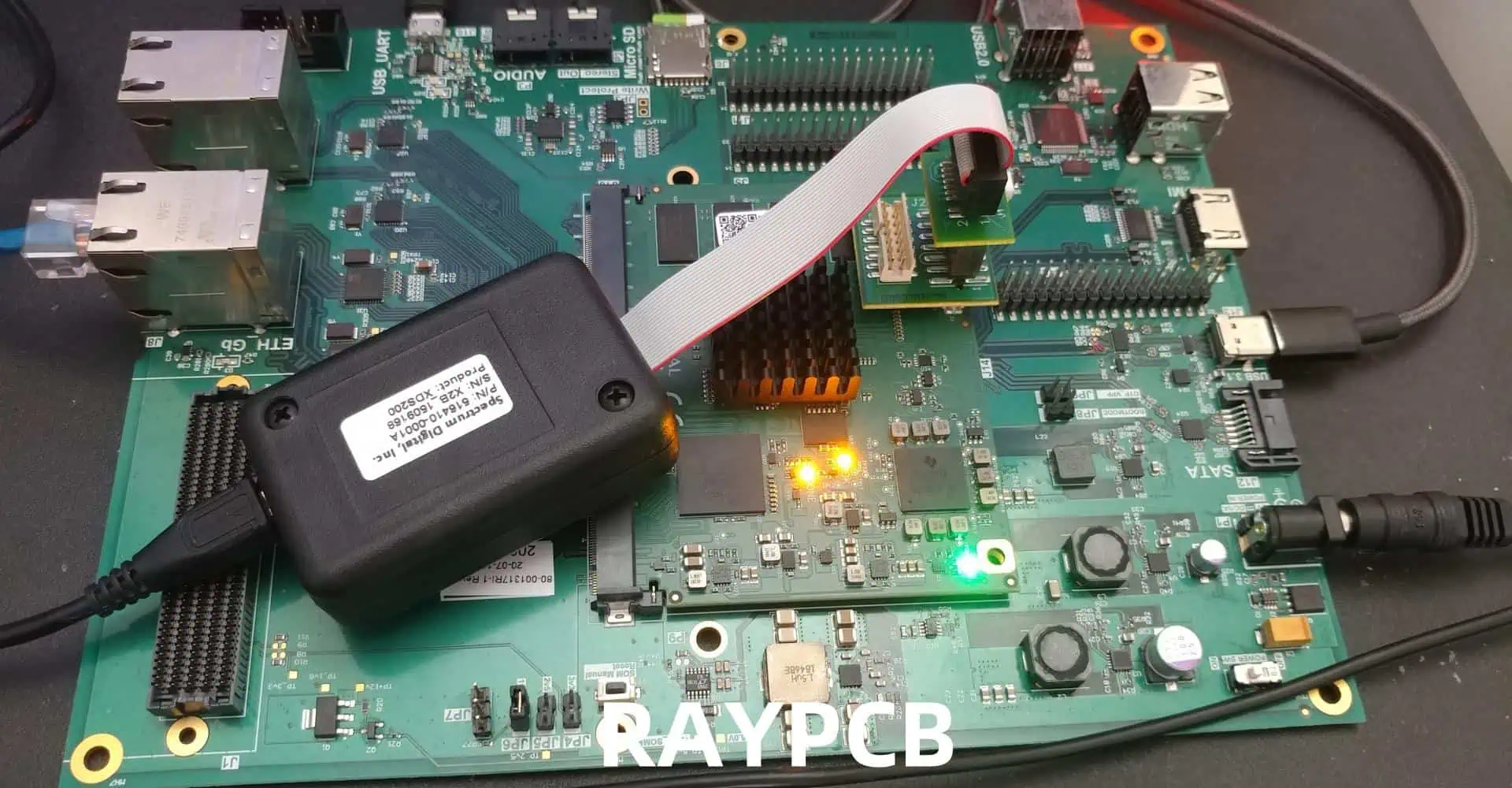
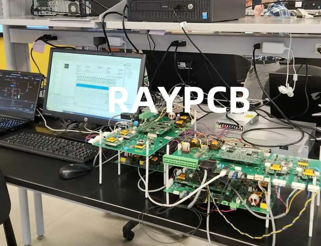
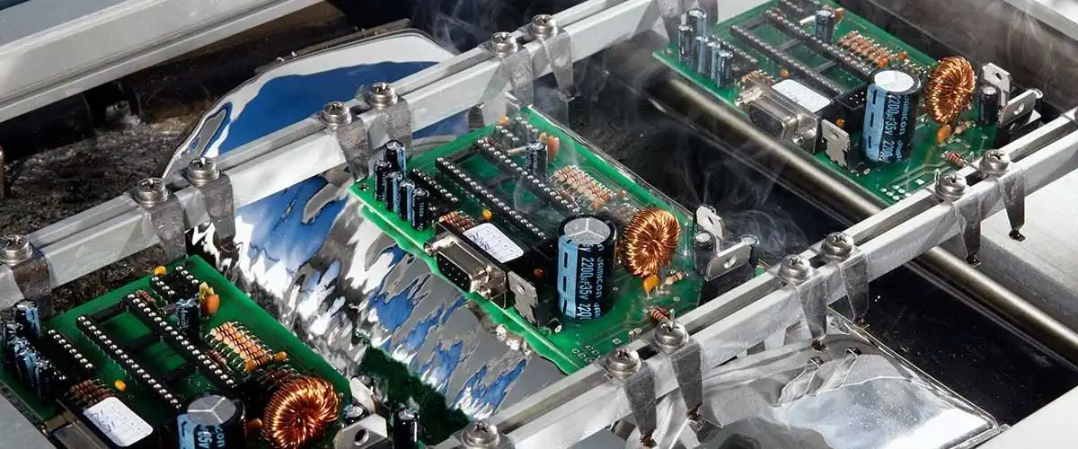
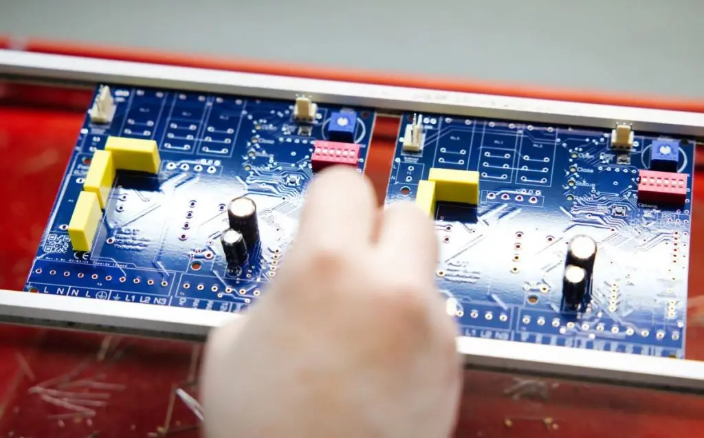
2.3 PCB Assembly (PCBA)
PCB Assembly is often the core of electronics product assembly. It typically involves two main technologies:
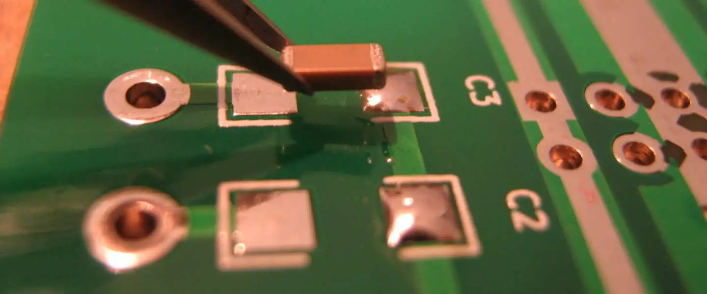
Surface Mount Technology (SMT)
SMT is the predominant method for assembling modern PCBs. The process includes:
- Applying solder paste to the PCB
- Placing components using pick-and-place machines
- Reflowing the solder in a specialized oven
SMT allows for higher component density and is suitable for automated assembly.
Through-Hole Technology
While less common in modern electronics, through-hole assembly is still used for certain components. The process involves:
- Inserting component leads through holes in the PCB
- Soldering the leads on the opposite side of the board
Through-hole assembly can provide stronger mechanical bonds for components that may be subject to mechanical stress.
2.4 Mechanical Assembly
Mechanical assembly involves integrating the PCBA with other structural and functional components. This stage may include:
- Installing the PCB into an enclosure
- Attaching displays, buttons, and other interface elements
- Connecting batteries or power supplies
- Installing heat sinks or cooling systems
- Assembling multiple subassemblies into a final product
Precision and attention to detail are crucial during mechanical assembly to ensure proper fit and function of all components.
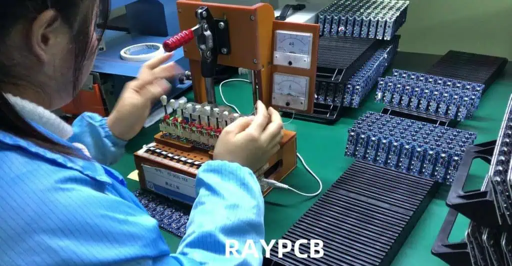
2.5 Testing and Quality Control
Rigorous testing and quality control are essential to ensure the reliability and performance of the assembled product. This stage typically includes:
- In-Circuit Testing (ICT) to verify component placement and connections
- Functional Testing to ensure the product operates as intended
- Environmental Testing to assess performance under various conditions
- Visual Inspection for cosmetic defects or obvious errors
Implementing comprehensive testing protocols helps identify and rectify issues before products reach end-users.
2.6 Packaging and Shipping
The final stage of electronics product assembly involves preparing the product for distribution:
- Applying any necessary labels or markings
- Installing protective films or coverings
- Packaging the product with appropriate cushioning materials
- Including user manuals, accessories, and other required items
- Preparing shipping documentation and arranging transportation
Proper packaging and shipping procedures protect the product during transit and ensure it reaches customers in optimal condition.
3. Types of Electronics Product Assembly
Electronics product assembly can be categorized into several types based on the level of automation and production volume. Understanding these types can help manufacturers choose the most appropriate assembly method for their specific needs.
Manual Assembly
Manual assembly relies primarily on human operators to perform assembly tasks. This method is characterized by:
- High flexibility for complex or varied assemblies
- Lower initial investment in equipment
- Suitability for low-volume or prototype production
- Potential for higher error rates compared to automated methods
Manual assembly is often used for:
- Highly customized products
- Products with frequent design changes
- Assembly tasks that require human judgment or dexterity
Semi-Automated Assembly
Semi-automated assembly combines human operators with automated equipment. This hybrid approach offers:
- Increased production speed compared to fully manual assembly
- Improved consistency and accuracy for repetitive tasks
- Flexibility to handle product variations
- Lower equipment costs compared to fully automated systems
Semi-automated assembly is common in:
- Medium-volume production runs
- Assembly of products with a mix of standardized and custom components
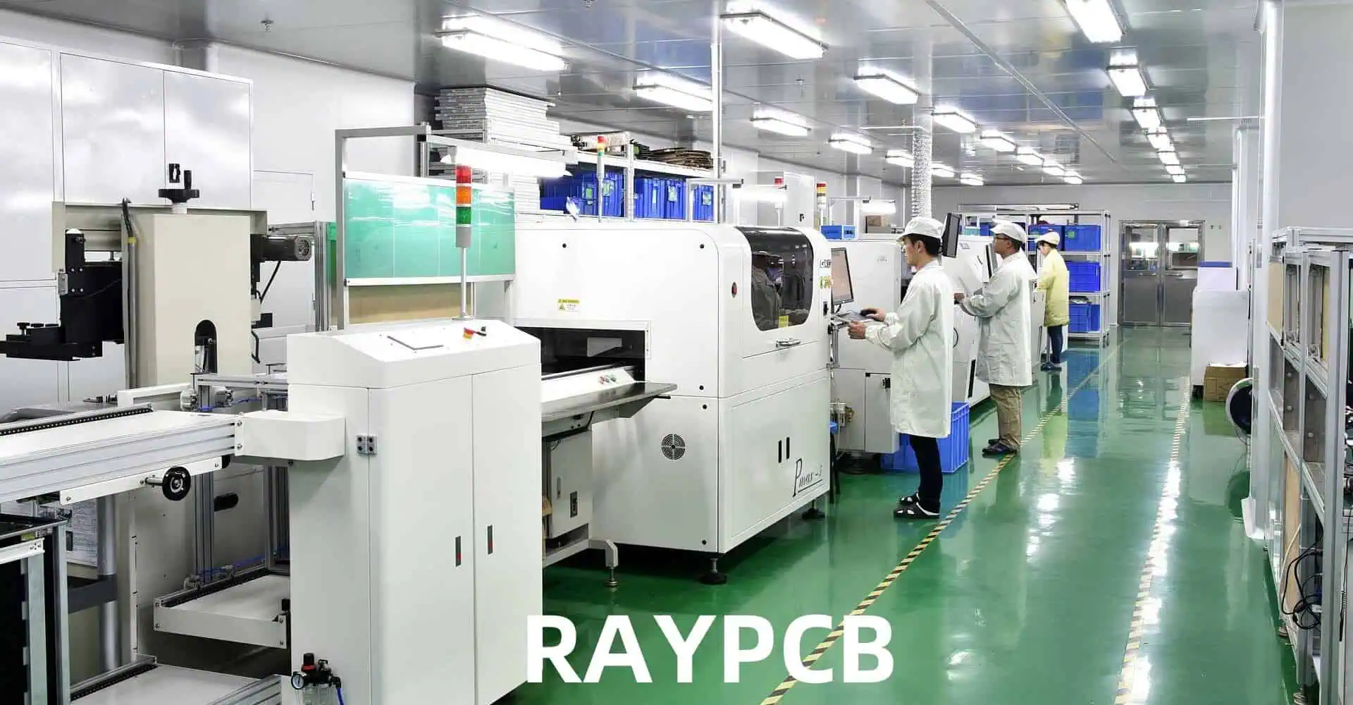
Fully Automated Assembly
Fully automated assembly relies on advanced machinery and robotics to perform most or all assembly tasks. Key features include:
- High production speeds suitable for large-volume manufacturing
- Consistent quality and precision
- Reduced labor costs over time
- Significant initial investment in equipment and programming
Fully automated assembly is typically used for:
- High-volume production of standardized products
- Assembly tasks that require extreme precision or speed
- Environments where human operators may be at risk
High-Mix vs. High-Volume Production
The choice between high-mix and high-volume production strategies depends on the nature of the products being assembled and market demands.
High-Mix Production
- Involves assembling a wide variety of products or product variants
- Requires flexible assembly systems and skilled operators
- Often employs manual or semi-automated assembly methods
- Suitable for industries with rapidly changing product lines or customized products
High-Volume Production
- Focuses on assembling large quantities of a single product or a few product variants
- Utilizes highly automated assembly lines for efficiency
- Requires significant upfront investment but offers lower per-unit costs
- Ideal for mass-market consumer electronics or standardized components
Choosing the right type of assembly process is crucial for optimizing production efficiency, maintaining quality, and meeting market demands. Manufacturers must carefully consider their product characteristics, production volumes, and available resources when selecting an assembly approach.
Read more about:
4. Key Equipment and Tools for Electronics Product Assembly
The success of electronics product assembly heavily relies on the use of appropriate equipment and tools. These technological assets not only enhance efficiency but also contribute significantly to the quality and reliability of the final product. Let’s explore some of the essential equipment used in modern electronics assembly:
Pick and Place Machines
Pick and place machines are the workhorses of automated PCB assembly. They are responsible for accurately placing components onto the PCB. Key features include:
- High-speed operation, capable of placing thousands of components per hour
- Precision placement, with accuracy down to micrometers
- Compatibility with a wide range of component sizes and types
- Vision systems for component alignment and verification
- Programmability to handle different PCB layouts and component arrangements
Reflow Ovens
Reflow ovens are crucial for Surface Mount Technology (SMT) assembly. They melt and then cool solder paste to create permanent connections between components and the PCB. Important aspects include:
- Precise temperature control across multiple heating zones
- Ability to create and maintain specific temperature profiles
- Nitrogen atmosphere options for improved solder joint quality
- Conveyor systems for continuous production
- Cooling zones to solidify solder joints properly
Wave Soldering Equipment
While less common in modern electronics assembly, wave soldering equipment is still used for through-hole components and some SMT applications. Key features are:
- Solder wave pumps to create a consistent wave of molten solder
- Preheating zones to prepare boards for soldering
- Conveyor systems to move boards through the soldering process
- Flux application systems for improved solder wetting
- Cooling systems to solidify solder joints
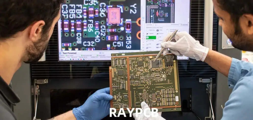
Inspection Systems
Quality control is paramount in electronics assembly, and advanced inspection systems play a crucial role:
Automated Optical Inspection (AOI)
- High-resolution cameras to detect defects in component placement and soldering
- Pattern matching algorithms to compare assemblies against ideal references
- Capability to inspect both pre and post-reflow assemblies
- Integration with production systems for real-time quality control
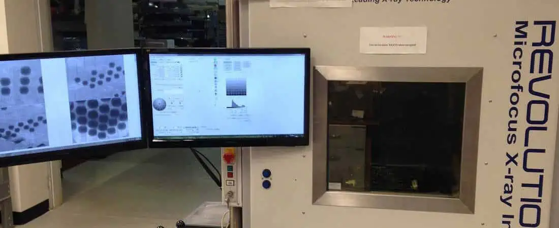
X-ray Inspection
- Allows inspection of hidden solder joints and internal component structures
- Crucial for inspecting Ball Grid Array (BGA) and other complex package types
- Capable of detecting voids, bridging, and other internal defects
- 3D imaging capabilities for comprehensive analysis
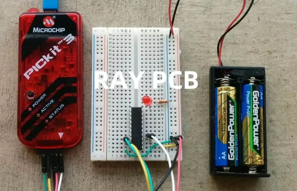
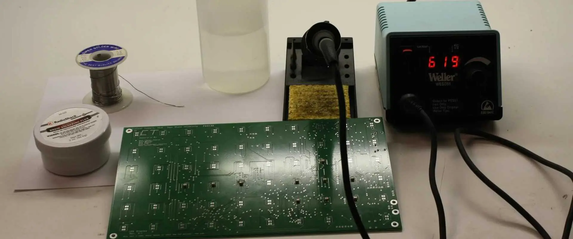
Hand Tools and ESD-Safe Environments
While much of modern electronics assembly is automated, hand tools and properly equipped workstations remain essential:
- ESD-safe workbenches and flooring to prevent electrostatic discharge damage
- Precision soldering irons with temperature control
- Magnifying glasses and microscopes for detailed work
- Tweezers and component handling tools
- Fume extraction systems for operator safety
- Specialized tools for coaxial cable assembly and wire stripping
Other Specialized Equipment
Depending on the specific products being assembled, additional specialized equipment may be necessary:
- Wire harness assembly machines
- Conformal coating application systems
- Ultrasonic welding equipment for plastic enclosures
- Automated screwdrivers and torque control systems
- Laser marking systems for product identification
Investing in the right equipment and tools is crucial for manufacturers aiming to produce high-quality electronic products efficiently. The choice of equipment should align with the specific assembly requirements, production volume, and quality standards of the products being manufactured.
5. Best Practices for High-Quality Electronics Assembly
Achieving consistently high-quality results in electronics product assembly requires adherence to a set of best practices. These guidelines ensure that the final product meets performance specifications, reliability standards, and customer expectations. Let’s explore some key best practices:
ESD (Electrostatic Discharge) Protection
Electrostatic discharge can cause severe damage to sensitive electronic components. Implementing robust ESD protection measures is crucial:
- Use ESD-safe workstations, tools, and flooring
- Require operators to wear ESD-safe clothing and footwear
- Implement proper grounding techniques for equipment and personnel
- Use ionizers in assembly areas to neutralize static charges
- Store and transport components in ESD-safe packaging
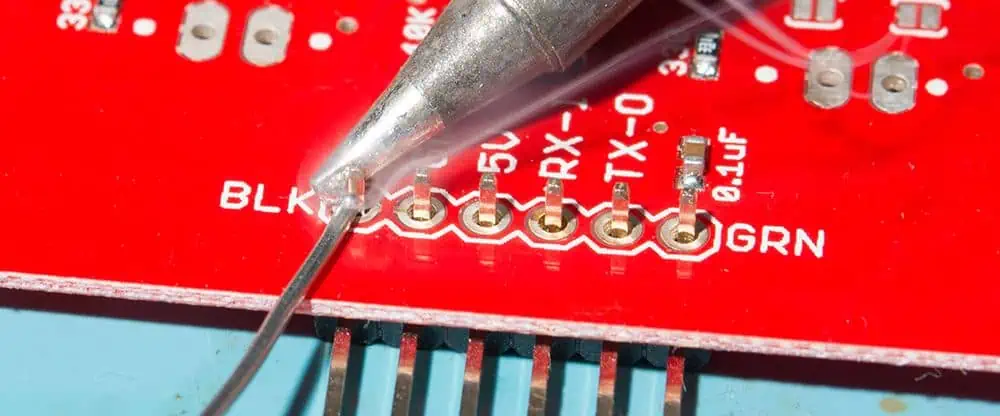
Proper Soldering Techniques
Soldering is a fundamental process in electronics assembly, and proper techniques are essential for reliable connections:
- Maintain correct soldering iron temperature for different component types
- Use appropriate solder alloys and flux for the specific application
- Ensure proper cleaning of surfaces before soldering
- Train operators in proper hand soldering techniques
- Regularly maintain and calibrate soldering equipment
Quality Control Checkpoints
Implementing multiple quality control checkpoints throughout the assembly process helps catch defects early:
- Incoming component inspection to verify quality and specifications
- In-process inspections during critical assembly stages
- Automated optical inspection (AOI) after component placement and soldering
- X-ray inspection for complex or hidden solder joints
- Functional testing of completed assemblies
- Final visual inspection before packaging
Staff Training and Certifications
Well-trained staff are crucial for maintaining high-quality standards:
- Provide comprehensive training on assembly processes and equipment
- Encourage staff to obtain industry-recognized certifications (e.g., IPC standards)
- Implement regular skill assessments and refresher training
- Foster a culture of continuous improvement and learning
Design for Manufacturability (DFM)
Collaborating with product designers to ensure manufacturability can significantly improve assembly quality:
- Review designs for potential assembly issues before production
- Standardize component types and sizes where possible
- Ensure adequate spacing for component placement and soldering
- Design PCB layouts that facilitate automated assembly processes
Environmental Control
Maintaining appropriate environmental conditions in the assembly area is crucial:
- Control temperature and humidity to optimal levels for assembly processes
- Implement proper air filtration to minimize dust and contaminants
- Ensure adequate lighting for detailed assembly work
- Maintain cleanliness standards in all assembly areas
Component Management
Proper handling and management of components contribute to assembly quality:
- Implement a first-in-first-out (FIFO) inventory system
- Store components in appropriate conditions (temperature, humidity, ESD protection)
- Use automated component storage and retrieval systems for efficiency and traceability
- Implement barcode or RFID tracking for component batches
Documentation and Traceability
Maintaining detailed documentation and traceability throughout the assembly process is essential:
- Keep detailed records of assembly procedures and any deviations
- Implement lot tracking for components and finished products
- Use Manufacturing Execution Systems (MES) for real-time process monitoring
- Maintain detailed test results and quality control records
Continuous Improvement
Adopting a mindset of continuous improvement helps maintain and enhance assembly quality over time:
- Regularly analyze defect data to identify recurring issues
- Implement root cause analysis for quality problems
- Encourage feedback and improvement suggestions from assembly staff
- Stay updated on industry best practices and new technologies
Supplier Quality Management
The quality of assembled products is directly influenced by the quality of sourced components:
- Establish rigorous supplier selection and evaluation processes
- Conduct regular audits of key suppliers
- Implement incoming quality control for critical components
- Develop partnerships with suppliers to improve component quality
By adhering to these best practices, manufacturers can significantly enhance the quality and reliability of their electronics product assembly processes. This, in turn, leads to improved product performance, customer satisfaction, and reduced warranty claims.
6. Common Challenges in Electronics Product Assembly
While electronics product assembly has become increasingly sophisticated, manufacturers still face a variety of challenges. Understanding and addressing these issues is crucial for maintaining efficient and high-quality production. Let’s explore some common challenges and strategies to mitigate them:
Component Shortages
The global electronics industry frequently faces component shortages, which can severely disrupt assembly processes.
Challenges:
- Production delays due to unavailable components
- Increased costs when sourcing from alternative suppliers
- Risk of counterfeit parts entering the supply chain
Mitigation Strategies:
- Develop relationships with multiple suppliers for critical components
- Implement long-term forecasting and advance ordering for key parts
- Consider redesigning products to use more readily available components
- Explore options for component stockpiling or vendor-managed inventory
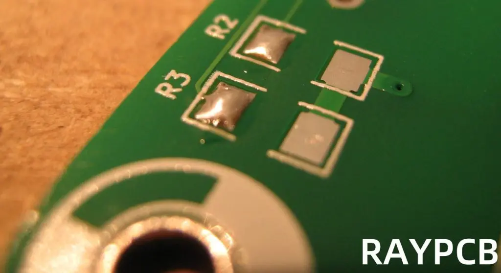
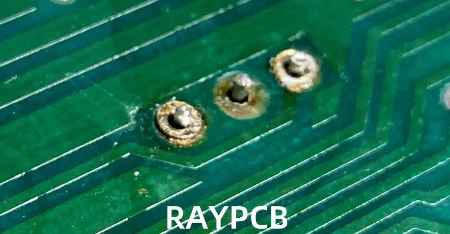
Soldering Defects
Soldering issues can lead to unreliable connections and product failures.
Common Defects:
- Cold solder joints
- Solder bridges
- Solder voids
- Insufficient solder
Mitigation Strategies:
- Implement proper thermal profiling for reflow soldering
- Regularly maintain and calibrate soldering equipment
- Provide comprehensive training for operators on soldering techniques
- Use automated optical inspection (AOI) and X-ray inspection to detect defects
- Optimize solder paste application processes
Testing Failures
Identifying and addressing testing failures is crucial for ensuring product quality.
Challenges:
- High failure rates increasing production costs
- Difficulty in diagnosing intermittent faults
- Balancing thorough testing with production speed
Mitigation Strategies:
- Implement comprehensive in-circuit testing (ICT) and functional testing protocols
- Use automated test equipment (ATE) for consistency and speed
- Develop clear procedures for failure analysis and root cause identification
- Implement statistical process control (SPC) to identify trends in failure rates
- Regularly review and update test procedures to address new failure modes
Miniaturization and Density Challenges
As electronic products become smaller and more complex, assembly becomes increasingly challenging.
Issues:
- Difficulty in handling and placing tiny components
- Increased risk of solder bridging due to tight spacing
- Challenges in inspecting high-density assemblies
Mitigation Strategies:
- Invest in advanced pick-and-place equipment capable of handling small components
- Use fine-pitch stencils and optimized solder paste application techniques
- Implement high-resolution AOI and X-ray inspection systems
- Consider using package-on-package (PoP) or system-in-package (SiP) technologies
Supply Chain Management
Effective supply chain management is critical for smooth assembly operations.
Challenges:
- Long lead times for specialized components
- Quality inconsistencies from suppliers
- Managing multiple suppliers across different geographic regions
Mitigation Strategies:
- Implement robust supplier evaluation and qualification processes
- Use supply chain management software for better visibility and forecasting
- Consider vertical integration for critical components
- Develop contingency plans for supply chain disruptions
Technological Advancements and Skill Gaps
Rapid technological changes can create skill gaps in the workforce.
Challenges:
- Difficulty in finding skilled workers familiar with the latest technologies
- Constant need for training and upskilling of existing staff
- Balancing automation with the need for skilled human operators
Mitigation Strategies:
- Invest in ongoing training and development programs for staff
- Partner with educational institutions to develop relevant curricula
- Implement mentorship programs to transfer knowledge from experienced staff
- Gradually introduce new technologies with adequate training periods
Environmental and Regulatory Compliance
Meeting environmental regulations and sustainability goals presents ongoing challenges.
Issues:
- Compliance with RoHS, REACH, and other environmental regulations
- Managing the transition to lead-free soldering processes
- Implementing sustainable manufacturing practices
Mitigation Strategies:
- Stay informed about current and upcoming regulatory changes
- Invest in equipment and processes compatible with lead-free assembly
- Implement recycling and waste reduction programs in the assembly process
- Consider design for environment (DfE) principles in product development
By addressing these common challenges proactively, manufacturers can improve their electronics product assembly processes, reduce defects, and enhance overall product quality and reliability.
7. Choosing the Right Electronics Assembly Partner
For many companies, partnering with an electronics manufacturing services (EMS) provider is a strategic decision that can significantly impact product quality, time-to-market, and overall business success. Here’s a guide to help you choose the right electronics assembly partner:
In-house vs. Outsourcing
Before selecting an EMS provider, consider whether outsourcing is the right choice for your business:
Advantages of Outsourcing:
- Access to specialized expertise and advanced equipment
- Scalability to meet varying production demands
- Potential cost savings on equipment and labor
- Focus on core competencies while leaving manufacturing to experts
Advantages of In-house Assembly:
- Greater control over the production process
- Protection of intellectual property
- Potentially faster turnaround for small production runs or prototypes
- Easier communication and collaboration with design teams
Key Criteria for Selecting an EMS Provider
When evaluating potential assembly partners, consider the following criteria:
1. Certifications and Quality Standards
Look for partners with relevant industry certifications such as:
- ISO 9001 for quality management systems
- ISO 13485 for medical device manufacturing
- AS9100 for aerospace industry standards
- IPC certifications for electronics manufacturing processes
2. Technical Capabilities and Equipment
Ensure the EMS provider has the necessary capabilities for your product:
- SMT and through-hole assembly capabilities
- Ability to handle your required production volumes
- Advanced inspection and testing equipment (AOI, X-ray, ICT, functional testing)
- Capabilities for any specialized processes your product requires (e.g., conformal coating, potting)
3. Industry Experience
Choose a partner with experience in your specific industry:
- Familiarity with relevant regulations and standards
- Track record of successful projects similar to yours
- Understanding of industry-specific challenges and solutions
4. Capacity and Scalability
Consider the EMS provider’s ability to meet your current and future needs:
- Production capacity that aligns with your volume requirements
- Ability to scale up production as your business grows
- Flexibility to handle both high-mix, low-volume and low-mix, high-volume production
5. Supply Chain Management
Evaluate the partner’s supply chain capabilities:
- Relationships with reputable component suppliers
- Ability to manage inventory and mitigate supply chain risks
- Experience in dealing with component shortages and allocations
6. Financial Stability
Ensure the EMS provider has the financial strength to support your long-term needs:
- Review financial statements if available
- Consider the company’s history and reputation in the industry
- Assess their investment in new technologies and equipment
7. Communication and Collaboration
Look for a partner that values open communication:
- Responsive customer service
- Willingness to collaborate on design for manufacturability (DFM)
- Transparent reporting on production status and quality metrics
8. Geographical Location
Consider the pros and cons of local vs. offshore manufacturing:
- Impact on shipping costs and lead times
- Ease of on-site visits and collaboration
- Potential language or cultural barriers
- Intellectual property protection laws in the manufacturing country
Questions to Ask an EMS Provider
When interviewing potential EMS partners, consider asking the following questions:
- What is your typical on-time delivery rate?
- How do you handle engineering change orders (ECOs) and revisions?
- What quality control measures do you have in place throughout the assembly process?
- Can you provide references from clients in our industry?
- What is your approach to component obsolescence management?
- How do you ensure compliance with environmental regulations?
- What level of visibility will we have into our production runs?
- How do you handle intellectual property protection?
- What are your capabilities for prototyping and new product introduction (NPI)?
- How do you manage supply chain risks and component shortages?
By carefully evaluating potential EMS providers based on these criteria and asking pointed questions, you can select a partner that aligns with your business needs and contributes to the success of your electronics products.
8. Trends and Innovations in Electronics Product Assembly
The field of electronics product assembly is continually evolving, driven by technological advancements, changing market demands, and the need for greater efficiency and sustainability. Understanding these trends can help manufacturers stay competitive and prepare for future challenges. Let’s explore some of the key trends and innovations shaping the industry:
Industry 4.0 and Smart Manufacturing
The concept of Industry 4.0, or the fourth industrial revolution, is transforming electronics assembly:
- Internet of Things (IoT) integration for real-time monitoring and data collection
- Artificial Intelligence (AI) and Machine Learning (ML) for predictive maintenance and quality control
- Digital twins for virtual modeling and optimization of assembly processes
- Cloud computing for improved data storage and analysis
- Augmented Reality (AR) for operator training and assembly guidance
Benefits:
- Improved efficiency and reduced downtime
- Enhanced quality control through data-driven decision making
- Greater flexibility in production processes
Miniaturization and Micro-Assembly
As electronic devices become smaller and more powerful, assembly processes must adapt:
- Advanced pick-and-place machines capable of handling components as small as 01005 (0.4mm x 0.2mm)
- Micro-LED assembly for next-generation displays
- Development of new soldering techniques for ultra-fine pitch components
- Increased use of system-in-package (SiP) and package-on-package (PoP) technologies
Challenges:
- Ensuring reliable connections with minimal solder volume
- Maintaining placement accuracy at microscopic scales
- Developing inspection techniques for ultra-small components
Eco-Friendly and Sustainable Manufacturing Practices
Environmental concerns are driving innovations in sustainable electronics assembly:
- Energy-efficient manufacturing equipment and processes
- Use of biodegradable and recyclable materials in product design
- Implementation of circular economy principles in electronics manufacturing
- Development of lead-free and halogen-free assembly processes
- Increased focus on product lifecycle management and end-of-life recycling
Benefits:
- Reduced environmental impact
- Compliance with evolving environmental regulations
- Improved brand reputation among environmentally conscious consumers
Additive Manufacturing in Electronics Assembly
3D printing technologies are finding applications in electronics assembly:
- Printed electronics for flexible and wearable devices
- 3D-printed circuit boards for rapid prototyping
- Additive manufacturing of custom enclosures and structural components
- Direct printing of conductive traces and antennas
Potential:
- Reduced time-to-market for new products
- Customization and small-batch production capabilities
- Integration of electronic and mechanical design
Automation and Robotics
Advancements in robotics are enhancing assembly processes:
- Collaborative robots (cobots) working alongside human operators
- Automated guided vehicles (AGVs) for material handling in assembly lines
- Vision-guided robotics for precise component placement and inspection
- Soft robotics for handling delicate electronic components
Benefits:
- Increased productivity and consistency
- Improved worker safety by automating hazardous tasks
- Greater flexibility in production line configuration
Advanced Materials and Packaging Technologies
New materials and packaging methods are enabling more advanced electronic products:
- Development of high-temperature and high-reliability solder alloys
- Increased use of flexible and stretchable substrates for wearable electronics
- Advanced thermal management materials for high-power electronics
- Wafer-level packaging technologies for improved performance and miniaturization
Implications:
- Ability to create more durable and reliable electronic products
- New form factors and applications for electronic devices
- Challenges in adapting assembly processes to new materials and package types
5G and High-Frequency Assembly
The rollout of 5G technology is driving innovations in high-frequency assembly:
- Development of assembly techniques for millimeter-wave (mmWave) components
- Increased use of advanced materials like low-loss dielectrics
- Implementation of shielding and isolation techniques for high-frequency circuits
- Specialized testing and quality control methods for 5G-enabled devices
Challenges:
- Maintaining signal integrity in high-frequency assemblies
- Managing thermal issues in densely packed 5G equipment
- Ensuring reliability of connections at higher frequencies
Customization and Mass Personalization
Market demands for personalized products are influencing assembly strategies:
- Implementation of flexible assembly lines capable of rapid changeovers
- Development of modular product designs for easier customization
- Use of late-stage customization techniques in the assembly process
- Integration of direct digital manufacturing for personalized components
Benefits:
- Ability to offer customized products at near mass-production efficiency
- Improved responsiveness to market trends and customer preferences
- Potential for new business models based on personalization
As these trends continue to evolve, electronics manufacturers must stay informed and adapt their assembly processes to remain competitive. Embracing these innovations can lead to improved efficiency, higher quality products, and the ability to meet the changing demands of the electronics market.
9. Cost Factors in Electronics Product Assembly
Understanding and managing the costs associated with electronics product assembly is crucial for maintaining profitability and competitiveness in the market. Let’s explore the key cost factors and strategies for optimizing them:
BOM (Bill of Materials) Costs
The BOM represents a significant portion of the total product cost:
- Electronic components (ICs, resistors, capacitors, etc.)
- PCB substrate
- Mechanical components (enclosures, connectors, etc.)
- Packaging materials
Optimization Strategies:
- Implement value engineering to identify cost-effective component alternatives
- Negotiate volume discounts with suppliers
- Consider second-sourcing for critical components to mitigate supply risks
- Regularly review and update the BOM to account for component price changes
Labor vs. Automation Costs
Balancing labor and automation costs is crucial for cost-effective assembly:
Labor Costs:
- Wages and benefits for assembly operators
- Training and skill development expenses
- Costs associated with human error and quality control
Automation Costs:
- Initial investment in automated equipment
- Maintenance and upgrades for automated systems
- Programming and setup costs for automated processes
Optimization Strategies:
- Conduct cost-benefit analyses to determine optimal automation levels
- Implement targeted automation for high-volume or precision-critical tasks
- Invest in training to improve labor efficiency and reduce errors
- Consider flexible automation solutions that can adapt to changing product lines
Testing and Inspection Costs
Ensuring product quality incurs various testing and inspection costs:
- Automated optical inspection (AOI) equipment
- In-circuit testing (ICT) systems
- Functional testing equipment
- X-ray inspection systems
- Labor costs for manual inspections
Optimization Strategies:
- Implement design for testability (DFT) principles to reduce testing complexity
- Use statistical process control to optimize testing procedures
- Invest in advanced testing equipment to improve efficiency and accuracy
- Develop clear criteria for determining necessary test coverage
Facility and Overhead Costs
Operating an electronics assembly facility involves significant overhead:
- Cleanroom maintenance
- Utilities (electricity, climate control)
- Equipment depreciation
- Facility rent or mortgage
- Administrative and management costs
Optimization Strategies:
- Implement energy-efficient practices to reduce utility costs
- Optimize facility layout for improved workflow and space utilization
- Consider outsourcing non-core functions to reduce overhead
- Explore lean manufacturing principles to eliminate waste
Supply Chain and Logistics Costs
Managing the flow of materials and finished products incurs various costs:
- Component transportation and handling
- Inventory storage and management
- Customs and duties for international sourcing
- Packaging and shipping of finished products
Optimization Strategies:
- Implement just-in-time (JIT) inventory management to reduce storage costs
- Optimize component packaging for efficient transportation
- Consider local sourcing to reduce transportation costs and lead times
- Use supply chain management software for better visibility and cost control
Quality-Related Costs
Maintaining product quality involves both prevention and failure costs:
Prevention Costs:
- Quality management systems implementation
- Employee training on quality procedures
- Preventive maintenance of equipment
Failure Costs:
- Rework and repair of defective products
- Customer returns and warranty claims
- Scrap and waste from rejected components or assemblies
Optimization Strategies:
- Invest in prevention to reduce more expensive failure costs
- Implement robust quality control processes throughout the assembly line
- Use data analytics to identify and address recurring quality issues
- Develop strong supplier quality management programs
New Product Introduction (NPI) Costs
Launching new products involves specific costs:
- Prototyping and sample production
- Tooling and fixture development
- Process development and optimization
- Compliance testing and certifications
Optimization Strategies:
- Use virtual prototyping and simulation to reduce physical prototyping costs
- Implement design for manufacturability (DFM) principles early in the development process
- Leverage existing production lines and equipment where possible
- Develop standardized NPI processes to improve efficiency
How to Optimize for Cost-Efficiency
To achieve overall cost-efficiency in electronics product assembly:
- Conduct regular cost analyses to identify major cost drivers
- Implement continuous improvement programs to enhance efficiency
- Invest in employee training to improve productivity and reduce errors
- Leverage technology for better cost tracking and forecasting
- Consider strategic outsourcing for non-core or specialized processes
- Implement lean manufacturing principles to eliminate waste
- Develop strong supplier relationships to negotiate better terms and ensure quality
- Regularly review and update assembly processes to incorporate new technologies and methods
- Balance automation with skilled labor to achieve optimal cost-effectiveness
- Focus on quality to reduce long-term costs associated with defects and returns
By carefully managing these cost factors and implementing targeted optimization strategies, manufacturers can improve their cost-efficiency in electronics product assembly while maintaining high-quality standards.
10. Case Studies: Successful Electronics Product Assembly
Examining real-world examples of successful electronics product assembly can provide valuable insights and inspiration for manufacturers. Here are three case studies from different industries showcasing effective assembly strategies:
Case Study 1: Consumer Electronics – Smartphone Manufacturing
Company: MobiTech Inc. Product: High-end smartphone
Challenge: MobiTech needed to ramp up production of their new smartphone model while maintaining high quality and managing costs in a competitive market.
Solution:
- Implemented a fully automated SMT line with advanced pick-and-place machines and AOI systems
- Developed a modular product design to allow for easier assembly and customization
- Utilized collaborative robots for final assembly tasks, working alongside human operators
- Implemented an AI-driven quality control system for real-time