Why Should You Use XCZU6CG-L1FFVC900I?

Xilinx Artix 7

The XCZU6CG-L1FFVC900I is a powerful SoC device. It combines an Arm Cortex-A53 64-bit quad-core processor with programmable Logic. It is from Xilinx. The following content will help you to know more about this specific part number.

Let’s start with its specification and how it is unique from the rest of SoCs.

 Unique Specifications

This SoC is part of the prestigious Xilinx Zynq UltraScale and MPSoC family. Its specifications are following

  • SoC has 256k logic cells as building blocks.
  • It has 1,248 DSP slices for better processing.
  • SoC has an 1,872 Mb/s DDR4 SDRAM interface for better connectivity.
  • 20.8 Mb block RAM for better storage is a good deal.
  • It has 1,152 18×18 multipliers and 144 GTX transceivers:
  • It has ARM Cortex-A53 MPCore 64-bit quad-core processor and ARM Cortex-R5 real-time processor, up to 600 MHz.
  • ARM Maliโ„ข-400 MP2 graphics processing unit makes it ideal.
  • It has a Dual-core ARM Cortex-A53 32-bit microprocessor for system management.
  • It has USB 2.0 and USB 3.0 controllers.
  • SoC has Quad SPI and NAND flash controllers.
  • Break down the alphanumeric code.
  • Herein lies an explication of the alphanumeric constituents of the part number XCZU6CG-L1FFVC900I. These are not ordinary codes or numbers; actually, they have explicit meanings.
  • XC represents Xilinx, a prominent producer of FPGA and SoC devices.
  • ZU6 alludes to the precise model or type of the ingredient. Plausibly, it is a member of the Zynq UltraScale+, a family of FPGA and SoC devices assembled by Xilinx.
  • CG refers to the exact form factor or package of the component. It is a ubiquitous variety of surface-mount packaging utilized for a wide array of electronic components. It is plausible that it belongs to the ball grid array (BGA) package.
  • L1FF is a combination of letters and digits. It can signify the velocity grade or performance level of the element. That’s why It is plausible that component.
  • Support a high-performance device with a rapid processing capacity.
  • VC900I is a character string that acts as a kind of identification mark or serial number that distinguishes the specific component from other components with similar numbers.

This breakdown will help designers or hobbyists to have some basic information.

Why Should We Use This FPGA?

1. Amazing Security Features

The XCZU6CG-L1FFVC900I has a variety of security features. It has a TrustZone security subsystem, secure boot, and encrypted memory. The TrustZone security subsystem provides a secure environment for running sensitive applications.

Similarly, a secure boot ensures that the device boots securely. In addition, encrypted memory provides protection for sensitive data stored in memory. That’s why you don’t need to worry about data security. It is secure with this device. As a result, it performs better. For example, if there is a security breach, then nobody will like it.

2. Development Tools for Better Customer Design

Xilinx provides a variety of development tools for the XCZU6CG-L1FFVC900I.

 Vivado Design Suite, which provides a complete design environment for creating and testing custom designs for the FPGA. Xilinx also provides a variety of IP cores and reference designs. As a result, you can create defines easily and accelerate the design process.

3. High-Performance Architecture

The XCZU6CG-L1FFVC900I provides high-performance processing and acceleration capabilities. In addition, the dual-core ARM Cortex-A53 processor provides a high-performance, low-power solution for general-purpose processing tasks. This FPGA is part of a wide range of applications. S data processing and machine learning are examples.

The cortex processor operates at a clock speed of up to 1.5 GHz. The Cortex-A53 is a power-efficient processor and provides high performance in a compact size. That’s why it is ideal for use in embedded systems and other low-power applications. In addition, the processor can run Linux. Similarly, it also supports other operating systems so easily. That’s why it provides a familiar environment for software development.

4. Acceleration For Graphics

ARM Mali-400 MP2 GPU provides hardware acceleration for graphics processing tasks. As a result, The GPU can handle complicated tasks. For example, video decoding and encoding, image processing, and the list are long.

5. Rich Set of Peripherals

 The XCZU6CG-L1FFVC900I comes with a rich set of peripherals. This help to integrate with different system such as Ethernet, USB, PCIe, and more. Similarly, these peripherals enable various communication and connectivity features in your application.

The XCZU6CG-L1FFVC900I FPGA supports a variety of connectivity options. For example, it includes Gigabit Ethernet, USB 3.0, SATA, and PCIe. The Gigabit Ethernet interface supports high-speed connectivity to networks. In addition, USB 3.0 interface provides high-speed data transfer to exterior devices. The SATA interface provides support for storage devices. Similarly, the PCIe interface supports high-speed connectivity to other devices, to graphics cards.

6. Programmable Logic and Excellent Memory

One of the key features of the XCZU6CG-L1FFVC900I is its programmable Logic, which provides the ability to customize the device for specific applications. The programmable Logic is based on Xilinx’s UltraScale+ architecture, which provides high performance and low power consumption. The device features a good number of logic cells, making it one of the most powerful SoC devices available.

The XCZU6CG-L1FFVC900I has a variety of memory options. It includes a

Four GB DDR4 memory controllers, Similarly, It also has 512 MB of Quad-SPI flash memory and sixty-four KB of non-volatile memory. The DDR4 memory controller provides high-speed access to memory. That’s why it is ideal for use in high-performance applications.

7. Low-Power Design with Adjustable Voltage and Frequency

FULL PCB MANUFACTURING Quote

The XCZU6CG-L1FFVC900I is known for low power consumption. Moreover, it is critical for battery-powered or energy-efficient.

The XCZU6CG-L1FFVC900I has power efficiency with a variety of features. It reduces power consumption. These features include dynamic voltage and frequency scaling. That’s why it easy to adjusts the voltage and frequency of the process. As a result, it matches the workload and power gating. So it shuts down unused parts of the device to save power.

Wrapping Up

The XCZU6CG-L1FFVC900I is a powerful SoC. Moreover, it brings together a quad-core Arm Cortex-A53 processor and programmable Logic. It provides superior processing capabilities and multiple memory options. That’s why it stands as an ideal component for a range of applications, including embedded systems. In addition, its vast capabilities make it a remarkably versatile device. As a result, it is capable of dealing with a wide range of complex and challenging computational tasks.

What is the Essence of Thermal Relief in a PCB?

Thermal Relief PCB

Heat dissipation concerns are on an increase in recent years, following the clustering or closer placement of components on circuit boards. Due to the proximity of these parts, it has become increasingly difficult to dissipate or keep away heat or thermal energy within the board. Today, one can use thermal relief pads to conduct heat away from the components.

In this article, we define thermal relief PCB, explain the important and explain how you can maximize it for the best thermal management results.

Thermal Relief PCB Meaning

Thermal relief, also called thermal relief pad and thermal pad, refers to the dedicated pad that manages heat/thermal transport in a circuit board.

Thermal Relief PCB Footprint

The primary function of the pad is to provide โ€œreliefโ€ to the PCB, in terms of the heat conduction capabilities. For this purpose, let us look at some of the factors that go into making the footprint.

The Location

The thermal relief PCB pad is designed as a large area of metal, meant for enabling the soldering of the metal to either the circuit board or the device.

It is also possible to solder or attach the metal to other surfaces, such as heatsink and a bolt.

Thermal Relief PCB Connection

The pad is usually connected between the heatsink and the heat-generating components. This is done to facilitate the further conduction away of the heat coming from these parts. That way, other components wouldnโ€™t be exposed to the heat and the negative effects.

Also, the thermal relief pad is commonly used in the location where there is either an existing connection between the fan-out via or the component pin to the copper plane.

The Copper Pour Connection

The argument is on whether the thermal relief pad is to be connected to the copper pour or to the tracks. These tips will help you make the right thermal relief PCB connections:

  • The thermal relief pad can be connected to the copper pour via a thermal connection. The connection is enabled by the use of 3 to 4 traces of copper spokes to have the pad attached to the surrounding copper.
  • For the best results, it is best to connect the pad to a few narrow tracks. The reason is that a direct connection to the copper pour makes the padโ€™s soldering difficult.

PCB Thermal Relief Guidelines

Designers ought to follow certain steps and guidelines, as these help them optimize the thermal relief pad for the best results.

Here are the cardinal points of utilizing the pad in your circuit boardโ€™s layout:

Thru-Hole Component Pins

Also called the thru-hole pins; these are the pins, which have been drilled through the circuit board for soldering purposes. The major concerns for using the thermal relief PCB pad for these pins are:

Cold Solder Joint

There is a risk of having a cold solder joint created. It is a result of the inability of the thru-hole pins from getting enough heat for solderability purposes.

The reasons for the inability to create good solder joints include:

  • The tendency of having heat pulled away from the pin by a split plane or any other small metal area. The resultant effect is that the area serves as a heatsink and takes away the heat.
  • The cold solder joints are created in multilayered PCBs, whereby an excessive amount of heat is required to extend beyond the several square feet of metal.

Forceful Heat Application

FULL PCB MANUFACTURING Quote

There is another risk of having heat forcefully applied towards the melting of the solder. This happens as a result of trying to โ€œunsolderโ€ the solder that was directly soldered to the larger areas of the metal.

The outcome of doing this is that the surrounding components/parts and traces are exposed to damages.

Surface Mount Pins

These are pins used for Surface Mount Devices (SMDs). Possible issues tend to arise with the smaller, two-pinned SMT devices. These problems arise due to the directly soldering of one of the pins to the larger area of metal.

Here are some of the reasons why PCB designers would embed a surface mount pad in a metal fill:

  • The embedding might give the best of electrical performance, but it comes at the expense of pulling away heat from the thermal relief pad.
  • There is also a risk of having one side of the solder melting faster than the other, due to the imbalance of the metal between the pins.

The best way to tackle the imbalance of the metal is to use several traces to connect a surface mount thermal relief pad. This proves to be a better option, rather than having it embedded into the large area of metal.

Metal Routing

There is a tendency that the metal wouldnโ€™t be enough to enable the connection of the spokes to the surrounding copper. This happens due to the following reasons:

  • The automated process of using CAD systems for adding the thermal relief PCB pads to the pins often impacts the pad. This also leads to limited space for the spoke-to-copper connection.
  • Certain power traces with lower conducting levels of current are often routed with the narrower traces.

Vias

There might be no need to use the thermal relief PCB with the vias, especially the ones that connect to the larger area fills, power planes and ground planes. The reason is that they donโ€™t often have pins soldered into them.

The primary consideration for using the pad for the vias is due to the following reasons:

  • If you are using nets that conduct higher current levels.
  • If this is the case, use the thermal relief PCB pad because some short power traces might facilitate excessive heat conduction to the surface-mount pins.

What is the Purpose of Thermal Relief in PCB?

You need to know when to use thermal relief PCB for your circuit board. The following are some of the benefits:

  • The pads aid in the manufacturability of circuit boards.
  • You can use thermal relief PCB pads to provide a robust electrical connection from the pad to the plane.
  • It also aids in the preventing of excessive heat dissipation into the metal plane.

Conclusion

Thermal relief pads are used in PCBs to bolster the restriction of heat flow into the copper pour, keeps the heat confined in the pad required for PCB component mounting and improving the padโ€™s solderability.

American Manufacturing Vs. Chinese Manufacturing on Electronic Devices

Electronic Devices Manufacturing

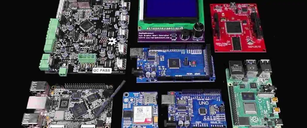
The global electronics manufacturing industry has kept on experiencing some trends and development. This industry has been producing devices, components, and equipment that contribute to technological advancements in the world. As the world keeps depending on technology, there is an increasing demand for electronics products.

In 2022, the global electronics market grew from $3554. 94 billion to $3739.37 billion in 2023. In the global electronics sector, China contributes a large percentage of revenue. This country is ranked among the top producers of electronic devices. In 2021, it accounted for 12.7 percentage of trade across the globe. Another leading producer of electronic devices is the United States. This country has a wide range of electronic manufacturing companies.

Electronics Device Manufacturing in China

China has continued to dominate the electronics manufacturing industry for some years now. This country is a integral manufacturing place for electronics despite its recent trade with the United States. China as a large manufacturing company exports about 50% of the laptops and cellphones across the globe.

Also, this country is the largest manufacturing destination of electronics across the globe. About three decades ago, the Chinese government maximized its low labor costs and big labor pool to produce more electronics. Since the integration of automation in advanced production facilities manufacturers began to get benefits from the rapid development of infrastructure in China.

China has continued to create partnerships with developed economies and an exporter of electronics to the United States.

What Electronic Devices Does China Produce?

Electronics panel board manufacturers

China is known to be a large producer of electronic devices. It produces various electronics products. These products range from consumer electronics to industrial components. Cities such as Dongguan and Shenzhen in the South have factories. Also, Shanghai and Choingun are home to factories. Here are a few examples of electronic devices produced in China.

Computers, laptops, and accessories

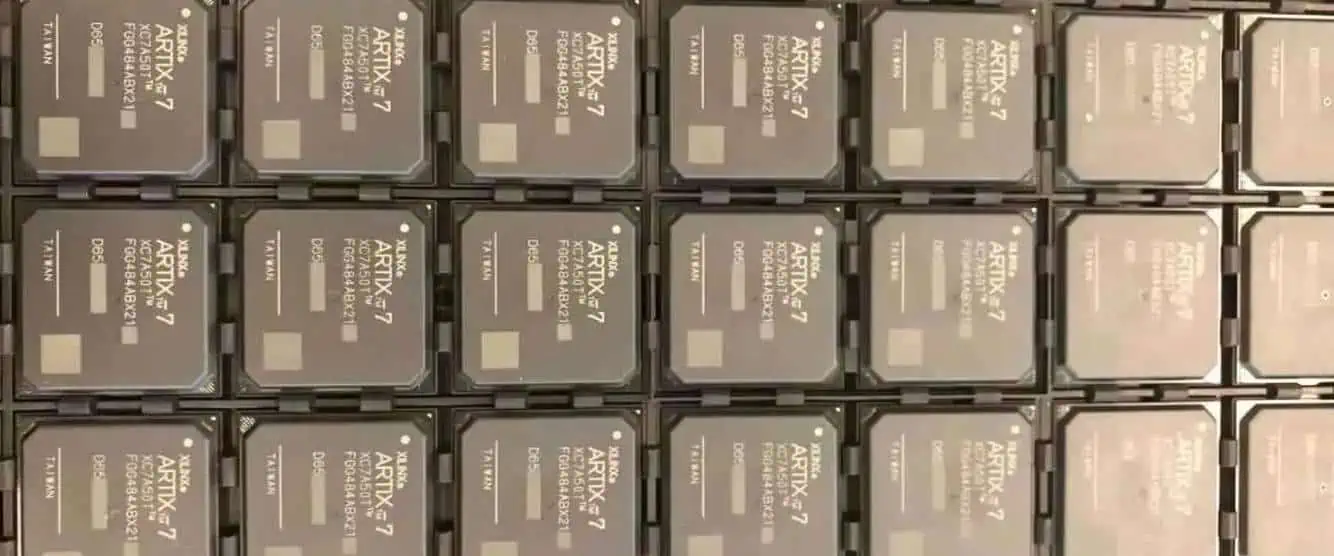
According to an estimate, China produces 90 percent of the laptop manufacturers globally. Also, this country produces other computer components and accessories. There are several Chinese brands like Huawei, Dell, and the likes. Also, the Chinese government has continued to make effort to bridge the the technology gap from foreign producers, particularly for semiconductors.

Despite China’s dependence on imported semiconductors, this country remains an good option for many world-class laptop brands. Kunshan and Chongqing are considered the two biggest clusters for laptop manufacturing  in addition to other popular electronic production hubs, like Dongguan and Shenzhen. These hubs are not only known for producing laptops, but also components and accessories.

These hubs specialize in the production of some electronics devices. This helps in making the sourcing process easy and as well create synergies.

Cellphones

China is ranked among the largest producers of cell phones. Mobile phone brands like Xiaomi, TCL, and Huawei are from China. These mobile phone brands ensured string manufacturing capabilities were established in China before they expanded their manufacturing and sales activities beyond the country.

Suppliers of related components like transistors and chips in China benefited from this expansion and growth. Also, China is popular for owning a large earth element reserve. This is crucial in manufacturing electronic components, especially cell phones. These resources help local manufacturers to have an added advantage over foreign producers.

Electronics Manufacturing Companies in China

China is unarguably the biggest manufacturer and exporter of electronics devices in the world. This country has a large supply chain, advanced manufacturing capabilities, and skilled labor force. With these, China has been able to develop its electronics manufacturing industry. For the past years, China has been a hub for the manufacturing of consumer electronic products and other electronic devices.

When it comes to quality and innovation, Chinaโ€™s electronics manufacturing company is leading the way. According to an estimate, the market value of Chinaโ€™s electronic manufacturing services would reach 500 billion dollars in 2023. Letโ€™s have a look at some of the top leading electronics manufacturing companies in China.

Huawei

Huawei is a global leader in electronics manufacturing. This Chinese based companyโ€™s mission and vision is to bring a fully connected world to everyone and organizations. The company which was founded in 1987 has vast experience and expertise in information and communications (ICT) devices and infrastructure.

Huawei is one of the most popular electronic companies in China and across the world. It has about 195,000 employees and operates in more than 170 countries. Huawei extends its services to over three billion people in the world. According to a report in 2020, Huawei is the best consumer electronics company throughout China. The comp[any is valued at 1.1 trillion yuan ($163.9 billion).

The product portfolio, solutions, and services offered by this company are secure and competitive. It offers extensive solutions across four main domains which are cloud services, telecom networks, smart devices, and IT.

Ryder Industries

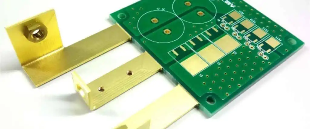
This electronics manufacturing company is based in Shenzhen, China. Ryder Industries offer various manufacturing services such as electronic manufacturing services, box-build assembly, and printed circuit board assembly. Since it was founded in 1979, It has continued to grow and expand its services.  Presently, the company is ranked among the leading providers of electronic manufacturing solutions.

Ryder Industries has two production plants in China and a total of 2500 workers. These production plants are equipped with sophisticated machines. Due to this companyโ€™s flexible and strong capability, Ryder Industries maintains timely delivery. Also, they ensure all the needs of their customers are met.

As an ISO 13485, ISO 14001, and ISO 9001 certified company, Ryder Industries ensures all of production processes and testing processes meet quality standards. From components and raw materials procurement to the last stage of the production process, quality standards are always adhered to.

Xiaomi

Xiaomi is a top leading electronics company that specializes in the production of consumer electronics. This multinational electronics company has its headquarter in Beijing. Founded in 2010, Xiaomi has been able to deliver quality electronic products to consumers. Xiaomi designs, produces, and sells smartphone, software and hardware products.

It product portfolio includes audio, camera, power bank, smartphone, and more. The Xiaomi Inc provides a wide range of products like phones, televisions, and more. This company has been able to build a strong ground in electronics manufacturing. Also, its electronics products have become so popular across several countries in the world.

As part of its achievement, this electronics company became Chinaโ€™s largest smartphone company. It has produced several series of smartphone commodities which include Mi Series, Mi Max Series, and more. Since Xiaomi was founded it has continued to deliver quality.

Goertek Inc

This Chinese technology company is involved in the research, development, and production of consumer electronics. Since it was founded in 2001, this company has continued to excel in its production and services. As a leading supplier of components for wearables, smartphones, and other consumer electronics, this company employs advanced production techniques and equipment.

Also, Goertek Inc produces high-end audio products which include headphones, wireless earbuds, and more. Over the years, this company has been able to expand its services and solutions across other fields like virtual reality, smart home devices, and artificial intelligence. Also, Goertek Inc has partnered with popular technology companies like Qualcomm and Microsoft.

Shenzhen Kaifa Technology Co. Ltd

Shenzhen Kaifa Technology Co. Ltd is a top electronic manufacturing company in China. This multinational electronic company has about 9 global manufacturing sites with 17,000 employees. The company which was founded in the year 1985 has been able to expand its services over time. Customers across the world can testify of the comprehensive electronic manufacturing services offered by this company. This includes production control, logistics support, process design, technology research & development.

This companyโ€™s product portfolio includes circuit boards for tablets, smartphones, ย and also components for smart meters. Furthermore, they produce various electronic devices like healthcare devices, security systems, and home products. Shenzhen Technology has invested hugely in research and development to contribute positively to the electronics industry.

Why is China a Leading Producer of Electronic Devices?

FULL PCB MANUFACTURING Quote

There are some factors that made China a large producer of electronics products.  Letโ€™s review the underlying factors behind this.

Large labor pool and low labor costs

The low labor cost in China is an advantage in electronics manufacturing. China has more labor resources and as such the cost if labor is much lower compared to North America or Europe. Also, the labor force in China is trained to out the quality of products in mind when producing electronic devices. This is one of the major reasons many electronic companies prefer to hire workers from China.

China is a low-cost country when it comes to electronic component sourcing. The wages of laborers in this country is about three times more than that of Vietnam. Also, a number of companies consider China as an integral hub for electronic manufacturing.

In bigger cities like Beijing and Shanghai, wages are known to be higher. Therefore, a good number of manufacturers target provinces in the central areas and in the South.

Large reserves of rare earth elements (REE)

China has the greatest reserve of rare earth elements in the world. Although it accounts for about 37 materials, these resources are crucial for the manufacturing of electronic products. Also, they are widely used in components like electronic displays,  computer hard drives, flat-screen monitors, and more.

Developed supply chain

One of the underlying factors that contribute to China’s large production of electronics is its developed supply chain. China has developed a unmatched business ecosystem that is difficult to find anywhere in Asia. Also, this developed supply chain is beneficial to manufacturers in the distribution and procurement processes.

Local Chinese companies are capable of producing most of the components integrated in electronics. This helps in reducing logistics costs. Asides from reducing logistics costs, the shorter lead times reduces the working capital. In the long run, this reduces the financial burden for businesses.

Disadvantages of sourcing electronics in China

Although, there are several advantages of sourcing electronics in China, there are some disadvantages. It is important to be aware of these disadvantages before procuring electronic components and products from China.

Communication barrier

Most times, foreign companies encounter communication barrier when they partner with Chinese suppliers. This can be quite frustrating and for this  reason many companies partner with local organizations that have staff that can understand their needs.

However, some Chinese organizations have now improved in English language recently. China, in general, has improved  โ€œlow efficiencyโ€ to โ€œmoderate efficiencyโ€ when it comes to  English language. This is favorable to global companies as they can now partner with Chinese companies. The business culture of China still remains different from the Western ones.

Shipping costs and lead times

In recent years, China has experienced disruptions in its major supply chain. The Covid outbreak in China and the container shortages contributed to these disruptions. The rate of shipping containers increased more than it was in the pre-Covid levels. Therefore, there have been diversification trends as more electronic companies seek to move their production to Southeast Asia or Eastern Europe.

Electronics Manufacturing in America

In terms of employment generation and export potential, America is one of the fastest growing electronic industries in the world. The United States contribute a large percentage of revenue to the global electronic manufacturing industry. There are a wide range of electronic companies in the U.S. These companies work towards the development and growth of the global electronic manufacturing industry.

The United States has experienced several projects going offshore due to high production costs and cheap labor during the past years. However, more businesses are beginning to realize the benefits they enjoy when they partner with electronic manufacturing services in the USA. You can minimize production costs to a great extent and as well prevent investing on infrastructure when you work with electronic manufacturing companies in the U.S.

The electronics industry in America is huge. This industry has some of the oldest and best electronic companies in the country. Also, these companies have gained popularity across the world to the extent that they have become a household name.

Furthermore, the boom in the global electronics industry has resulted in the emergence as well as the development of some electronic companies in the world. Countries like China and Japan are also major players in the electronics industry.

Advantages of Electronic Manufacturing within America

Cost difference is negligible:

The increasing cost of transportation in Asia has decreased the price gap that exists between local and offshore pricing. For instance, electronics manufacturing companies in the U.S are competitively-priced and as such gives you the opportunity to optimize cost and production time.

Quality assurance:

Manufacturers are beginning to have a rethink about reshoring in America due to quality issues in highly-regulated industries like aerospace, medical, And aviation among others. Electronic manufacturing companies in America ensure they electronic products are manufactured without compromising quality. Tip electronic manufacturing companies in America offer the best quality standards.

Advanced PCB design engineering capabilities:

Electronic manufacturing companies in America are capable of meeting the requirements and specifications of highly specialized industries. From manufacturing equipment to semiconductor testing and industrial equipment, these companies have what it takes to serve a wide range of industries.

Employment generation:

In the past, many facilities were shut down due to offshoring and this resulted in, job losses. A good number of manufacturers are beginning to realize the intrinsic value of providing huge support to local electronic manufacturing companies in the USA.

Top Electronics Manufacturing in America

PCB prototype assembly suppliers

Epec Engineered Technologies

Epec Engineered Technologies is a great choice when looking for OEM product solutions. As an electronics company based in the United States, this company offers top-notch electronics manufacturing services. By offering advanced technical resources, fast delivery in the industry, and an effective manufacturing platform, Epec Engineered Technologies has been able to offer innovative solutions that offer highly reliable products.

Also, this company is a leading producer of user interface products, cable assemblies, electronic fans, custom battery packs, and printed circuit boards. This company has been able to earn the trust of their customers due to their flexible manufacturing capabilities, engineering services, and 24/7 customer support.

Epec Engineered Technologies has employees across the world; these employees are dedicated to creating innovative solutions that offer the best quality products.

Dell

Dell is ranked among the top PC suppliers. It deals with the development as well as the manufacturing of computers as well as different computer-related products. The company is headquartered in Texas. This company lays much emphasis on customer support by integrating a risk-free return policy. Over time, Dell expanded into the international markets after investing in research and development.

In the early 2000s, Dell expanded its products and solutions to include digital cameras, televisions, and a number of computer-related products. Dell was renamed as Dell Inc in  2003. This signified its move into a broader spectrum in the consumer electronics industry.

One of the benefits of working with this company is that it offers high-quality personal computers at very competitive prices. Also, the company ensures all of its products undergo the necessary tests before they are approved for sales. Dell and another firm acquired an American corporation, EMC.

Apple Inc

Apple Inc is a reputable brand in the United Sates. It is known for designing, manufacturing, and supplying electronic products like personal computers, smartphones, wearable devices, and tablets. Also, this company provides software related services and third-party digital content.

Its product portfolio comprises Mac, Apple Watch, Iphone, Apple TV, Mac, Ipod, and more. Apple provides a wide range of consumer software applications like macOS, iCloud, iOS, and AppleCare. Furthermore, Apple delivers and sells digital applications and content via Apple News, Apple Music, App Store, Apple TV, and Apple Arcade.

Furthermore, this company offers cloud services, advertising services, and payment services. In 2022, report has it that Apple would be partnering with Samsung Electro-Mechanics to produce the M2 chip. Apple is known for producing high-quality products. This company doesnโ€™t compromise the quality of its products.

HP

This is another popular electronics manufacturing company in the United States. With its cutting-edge technology, this company delivers a wide range of consumer electronics such as digital cameras, laptops, computers, and more. HP stands for Hewlett-Packard.  HP was founded in 1939. With a long-standing experience in the production of electronic computers.

Also, this company specializes in the production and development of software and hardware components. HP also provides other computer-related products such as desktops, accessories, and printers. As an American-based electronics company, HP works with a dedicated team of engineers and developers who are dedicated to producing quality computer products.

HP company ensures all the needs of its customers. It manufactures its products to suit the increasing demands in the electronics industry. The vision of HP is to make life much easier and better for everyone through its innovation.

U.S Manufacturing Vs China Electronics Manufacturing

In terms of electronics manufacturing, China remains at the top. This country has a good number of electronics manufacturing companies. Recently, thereโ€™s been a huge and tremendous change in the electronics manufacturing field in this country. China has continued to lead the world as regards its electronic manufacturing output.

The electronics industry in America is huge. This industry has some of the oldest and best electronic companies in the country. Also, these companies have gained popularity across the world to the extent that they have become a household name. Highly ranked electronic companies in the United States benefit from a good share of the international electronics industry.

When it comes to quality and innovation, Chinaโ€™s electronics manufacturing company is leading the way. According to an estimate, the market value of Chinaโ€™s electronic manufacturing services would reach 500 billion dollars in 2023.

Conclusion

The electronics manufacturing industry keeps experiencing growth. As more companies are emerging, the annual growth rate in this industry keeps increasing. China is home to a wide range of electronics manufacturing companies. There are other countries with electronics manufacturing companies. However, some countries are leaders in electronics manufacturing. We have evaluated electronics manufacturing in China and the U.S. China has more advantages compared to the United States.

What is PCB Busbar or PCB Stiffener Busbar in Electronics?

PCB Busbar

PCBs and Circuit boards serve as crucial elements of Worldsโ€™ most advanced technologies. Electrical components in medical, military, telecommunication, aerospace, and advanced technology fail if PCB malfunctions or breaks.

Life would be at risk if the PCB goes wrong and starts malfunctioning. Therefore, it becomes vital to make a break, damage, and malfunctioning-free PCB to reduce the risk of danger.

A busbar typically represents a metallic bar or strip. It comprises brass or copper that performs electrical conductivity across circuit boards, electrical components, power units, and battery banks. Engineers specially design these strips to conduct an adequate amount of electricity than a conventional PCB trace.

Busbars also spell differently, like busbar, BusBar, busbar, and busbar. 

A stiffener represents a substance or metallic sheet, or panel. It incorporates the PCB to enhance its rigidity and gives strength to the board. It plays an important role in PCB, which is used in harsh environments. 

Busbar not only serves as an electrical conducting bus but also gives structural integrity or strength to a PCB. Whereas, Stiffeners does not serve as a bus because it must have brass with IACS 28%. The manufacturers and engineers of E-Fab use the Photochemical etching technique to create stiffeners and busbars. The photochemical etching also represents PCM or photochemical machining. These products enhance the old process and designs of CCI.

Advantages Of Using PCB Busbaror Stiffners 

pcb stiffener busbar

Busbars possess various advantages. It serves as a vital component of conducting electricity, particularly when reducing the cost, simplifying the electrical distribution process, and demands greater flexibility. They come in a variety of sizes and different coatings, like aluminum and copper. The type of material, size, and shape of a busbar determine the capacity of current it can carry.

ยท Compact & Robust 

Although a busbar costs more than a coil harness yet, it lasts longer and does not need a replacement at any time sooner.

ยท Distributes Power Efficiently

The efficiency of energy and power distribution has become the main focus of many industries in the modern technological era. However, the busbar helps in reducing the consumption of energy well. Because of its integrated nature, it can easily adapt to the integration of renewable energy, which is quite intriguing to consider in this advanced era of energy.

ยท Copper Busbars Are Conductors

Because of the high conductive ability of copper, it serves as an ideal and most popular material to make busbars as the busbar needs to conduct the electricity easily with the moving electrons. Copper is a strong material that has the ability to bear the harsh environment and high temperatures. These qualities also enhance its life durability. 

ยท Easily Customizable

Busbar provides various options for mechanical design. They are highly versatile products. This means they are highly found in education, hospitals, and factories. Tight space and compact devices require substitute electrical distribution, and busbars serve the purpose right.

Because of its highly resilient and robust quality, the busbar can survive extremely harsh weather. This makes them ideal to use in electrical switchyards and substations. 

ยท Cost-Effective 

The installation of a busbar can cost much, particularly when creating a whole new network, because the busbar very rarely needs replacement. Even during the installation of new points, it eliminated the need for construction because of its unit’s freedom. This saves both construction costs and construction time. 

We are highly able to build and design your custom-specified bars, which ensure high-quality standards according to the scope and project. Our skilled and professional engineers can tailor your specifications into well-functioned busbars and provide a high-quality PCB and PCBA.

What Is A Copper PCB Busbar?

Copper has incredibly versatile qualities, which include low thermal and electrical resistance and high mechanical strength. It also possesses great resistance to wear and tear failure. This makes copper an ideal component to use in busbars for high electrical conductance, for example, in panel boards, busway enclosures, and switchgear to distribute high electrical current. Moreover, it can also be used in almost all applications with high electrical conductance. 

Is An Aluminium PCB Busbar As Best As Copper?

Aluminum busbars use lighter material to produce in mass which makes them more cost-effective than copper busbars. It serves as an ideal busbar for companies where installation, budget, and max weight concern them. Aluminum is lightweight and has a more open area. It does not conduct as well as that copper. To reach the copper busbar criteria, a conductor size must be large, which in most cases is not feasible and practical. Aluminum busbars act as a great alternative and offer various positive benefits. Yet, copper remains the foremost and better choice in almost all aspects.

What Are Laminated PCB Busbars?

FULL PCB MANUFACTURING Quote

The laminated busbar contains fabricated layers of copper. Each copper layer is separated with thin material dielectric and has a unified laminated structure. Each layer goes through high temperatures and forces into an incorporated component. This layer component offers various benefits over a one-layer cable conductor or busbar. The application and size of laminated busbars vary from a tiny coin size to several-foot-long multilayer busbars.

Why Are U-Shaped PCB Busbars Popular?

The busbars in U-shaped are highly popular because of their incredible quality in delivering reliable and continuous connection. It also maximizes the possible locations. Some efficient benefits of U-shaped busbars include the following:

The U-shape offers a greater level of weight distribution. It copies the distortion and noise from a greater force. It allows reconfiguration, relocation operation, and simple expansion. The U-shape offers constant pressure at each joint end. This shape allows solid connection while eliminating the demand for daily maintenance.

PCB Busbar and Stiffener Materials

The stiffener of PCB usually uses materials like FR-4, aluminum, polyimide, and stainless steel. Each material offers distinct benefits and characteristics according to the application. 

1. Polyimide Stiffeners

The stiffeners of polyimide enhance the thickness of the ZIF connector to offer complete support to the connection fingers. During the process, the polyimide stiffener contours the joints of electrical components and gives tolerance to the thickness of bending.

These polyimide stiffeners prove helpful in limiting Printed Circuit Board bending ability to enable it for the final installation of PCB assembly. Polyamide stiffeners serve as ideal for hole location as it gives extra wear and tear resistance during errors. 

Moreover, it also gives greater solder resistance, bond strength, and hole locations for stiffeners over the opposite side of gold finger insertion. You can easily pick a non-attached and non-laminated part of the stiffener from the surface of the flex PCB. After choosing the part, put the connector finger of the flex board to the Socket or connector of ZIF.

2. FR-4 Stiffeners

FR4 stiffener offers various benefits. The main goal of using these stiffeners in a flex board is to give full flat support during the pick-and-place and reflow process. It also gives support to the connected areas. Moreover, it also gives full support to the through-hole electrical components to reach the solder pad. Furthermore, the same positioned holes inside the flex boards and stiffeners have similar diameters. In such cases, enlarge the stiffener access holes. 

The enlargement can range up to 0.15 mm on both sides. This prevents manual bonding from misalignment. This process requires the prestack of adhesive or prepreg, registration, and drilling.

3. Aluminum & Stainless Steel 

Both stainless steel and aluminum metallic stiffeners prove ideal for flexible boards. They possess abilities like robustness, capability, formability, and resistance. Moreover, metal mostly hardens the panel of connectors and provides easy assembly. But they are much more costly and take a longer time to process than the FR4 and polyimide.ย 

Aluminum offers great heat dissipation, whereas stainless steel stiffens the specific part of the board. The process of bonding for aluminum stiffeners needs milking, registration, prepreg pre-stacking, and drilling. At the same time, stainless steel needs drilling, registration, prepreg pre-stacking, and laser cutting.

Things to Consider to Pick the Best PCB Busbar Manufacturing Company

Choosing an ideal manufacturer of PCB stiffener not only gives quality products but also determines the overall cost of PCB. However, the following are some factors you must keep in mind while choosing a specific manufacturer. 

Check the profile of the company. Check whether they provide diverse and high-quality PCB stiffeners, as it determines your expectations and what you will get from them. Evaluate the standards and certification of quality management. The company must own resources, advanced technology, and enough capacity to produce high-quality stiffeners. They must follow the standards. 

Some manufacturers aren’t ready to adopt advanced technologies, so check whether they have a diverse quality of adaptation with an advanced era. For this, see their advanced technologies and method of working, as this predicts their fast and reliable nature of adapting the technologies. Thus, it automatically gives you high-quality and high-standard PCB stiffeners based on your needs. 

Price always plays an important factor to consider. Generally, it’s the manufacturer’s responsibility to use such resources and technologies which reduce the production cost. Therefore, you must not need to spend extra budget on sourcing stiffeners. 

We provide the most reliable and high-quality PCB stiffener to our clients. We not only maintain the quality but also focus on reducing the overall cost in every manner.ย 

Can PCB Busbar Affect PCB Performance?

high-current-pcb-design

Stiffeners directly enhance the performance and efficiency of PCB. This happens when it reduces board stress which directly affects the functionality of the board. Moreover, it increases the reliability of the board. Without stiffeners, PCBs become fragile and sensitive. Therefore, it mainly protects the electrical components and strengthens the connections. 

These benefits play a vital role as reinforcing the whole PCB does not suit well. Because it enhances the weight of the board and makes it rigid. The main purpose of stiffeners is not only to make the board rigid but to enhance its functionality and make its components durable to withstand the device. In simple words, with stiffeners, PCB remains rigid, does not break or suffer any damage from excess use and enhances its durability.

How To Use Board PCB Busbar On Your Circuit Board?

Put the board stiffener on the similar side of the through-hole electrical components as it provides holes and easy access to the solder pads. Moreover, you can also put the PCB stiffener over both sides, but this method requires a special type of configuration during the assembly of the PCB. Furthermore, such boards also need FR4-type stiffeners over the array boards as it aids in eliminating the additional tooling plates. 

Moreover, it also allows flexible PCBs to go through the automatic process of assembly just like their solid counterparts. At the same time, the process of attaching the stiffener to the board requires pressure and heat. Due to pressure, use pressure-sensitive glue to install the stiffener. Therefore, two widely used board stiffener adhesives for installation include Pressure-sensitive glue and Thermally bonded glue. Moreover, ensure to take some factors into account before selecting any adhesive for your PCB stiffener. These factors comprise thermal exposure, the capacity for adhesiveness, and chemical resistance.

Conclusion

PCB stiffeners provide various benefits to the Circuit board. They enhance the connectivity of connectors, provide durability to the board, and act as a connector. Moreover, you can also use a stiffener on specific areas to enhance the strength without putting it on the whole PCB. Furthermore, any wrong installation directly affects the overall performance and efficiency of the board. Thus, you can utilize various techniques and glows to install the stiffener onto the board.

Comparing Polyamide and Polyimide: What’s the Difference for PCB?

Arlon polyimide

There are some excellent chemical substances that have an amazing ability to resist temperature. These typical substances are polyamides and polyimides. These are basically thermoplastic elastomers that are crucial for some technical domains.

 One main difference between these two comes in their chemical properties. Their structures are not similar. The chemical groups of these two polymers are different, which sets them apart from each other.

 There are some common properties of these two substances, including electrical attributes, physical characteristics, and impressive thermal stability. 

What is Polyamide?

Polyamides are common elastomers. They have a special chemical group called the amide group in their chemical structure. One fine example of polyamides is Nylon. It is an ancient polymer that has crucial applications in different domains.

 There are some excellent properties of these substances that come in handy for major uses. These are:

  • Higher temperature control
  • Heat aging ability
  • Solvent resistance
  • Good modulus/impact abilities
  • Less coefficient of friction
  • Higher resistance to abrasion

What is Polyimide?

Polyimide Stencils

Polyimides are another type of polymers. They are different from Polyamides due to their chemical group. The chemical group for Polyimides is the imide group. There are two further categories of Polyimides.

 These can have open chains and closed chains. You cannot expose them to hot temperatures for a long period of time. 

 There are some salient chemical properties of polyimides that you should know. These include:

  • Good thermal stabilization
  • Electrical conductance
  • Resistance to abrasion and solvents

Due to the aforementioned properties, polyimides have important applications in different which are:

  • Films for insulation
  • Laminations
  • Strong adhesives
  • Molded parts
  • Robust modulus threads
  • Composites for extremely hot temperatures

PCB Material of Polyamide and Polyimide

Polyimides are chemical derivatives of imide monomers. Polyimides can be artificial or natural. It mainly depends on the type of product you want to use polyimides for. Some simple examples of polyamides are silk and wool. 

However, when it comes to producing PCBs, artificial polyamides are efficient on all counts. You can develop artificial polyamides by combining imide chemical structures. Keep in mind that bis maleimides and maleic anhydride are important for making artificial polyamides. 

The additives you will use in this process determine the type of polyamide as the final product. 

Here you will find some good examples of artificial polyamides:

ยท        Pure Polyimides: Pure Polyimides are basically 2nd generation polyimides. You don’t have to brominate these, unlike other polymers. It is much more time-saving to produce second-generation polyimides. Due to this, these are important for thermal stabilization and temperature control. 

ยท        3rd Generation Polyimides: These polyimides are all those substances that can prevent flammability. It is important for some electronics as they can catch fire due to electrical glitches and short circuits. However, these are not much impressed with thermal stabilization. You can rely on them for fast production because of their low temperature. 

ยท        Filled Polyimides: Filled polyimides come with a filler. They are excellent for resisting thermal resistance and have more flexibility. The purpose of a filler is to keep the resin damage as minimum as possible. It prevents cracks when it comes to drilling, which can lead to further problems if not handled in time. 

ยท        Low-Flow Polyimides: These polyimides include different types of resins that are important for opposing flexibility when needed. 

When Should Polyamide And Polyimide Be Used?

FULL PCB MANUFACTURING Quote

Polyimides have increased the market demand over the years. The products, including polyimides, are useful for their durability and flexible nature. However, there are more factors that make polyimides favorable for many PCB producers around the globe.

You must determine the characteristics of your PCBs when selecting a particular polyimide so that you will be able to save time, money, and energy due to this.

Below are some factors that will help you in this regard:

ยท        Excellent Flexibility: Polyimides have no parallel when it comes to increasing the flexibility of rigid and flexible PCBs. As polyimides already have excellent flexibility, they never fail you in this pursuit. 

ยท        Excellent Tensile Strength: These polymers can impressively oppose warping. When your devices need a higher degree of durability, use polyimides to ensure their robustness and strength on all counts. 

ยท        Very Thermally Stable: Polyimides show excellent stabilization when exposed to hot temperatures. Besides, they are good in thermal conductivity, which helps in alleviating damage during PCB production

ยท        Resistant to Chemicals: Polyimides are stable chemical polymers. It means that you can combine them with corrosive and unstable substances without any fear. 

ยท        Highly Durable: Not only Polyimides can handle hot temperatures and unstable chemicals. These never fail to perform naturally under stress. No matter the external environment, their shapes never undergo drastic changes. Due to this, these are important for devices that perform extreme functions in different domains. 

Applications Of Polyamide Material

All types of polyimides have important use cases in different industries. You can find polyimides in vehicles, clothes, and consumer electronics. However, one major application of these remarkable polymers is in PCBs. The polyimides pass on great properties to the rigid and flexible PCBs. 

Below are some significant applications of polyimides that you must know:

ยท        Computer Electronics: Computing devices like PCs and desktops need to be flexible and robust to perform different tasks. Such properties help these devices to deliver quality performance under stressful conditions. However, sometimes these devices can become overheated. In this case, polyimide PCBs help in cooling down these devices. These are important to save them from possible damage due to heat. 

ยท        Automotive Electronics: Modern automotive electronics always rely on durable and heavy-duty electronic parts. These components include polyimide PCBs that absorb vibrations to a large extent. Not only this, these are important for cooling down these parts from the heat generated by a device.  

ยท        Consumer Electronics: Consumer electronics like smart devices include rigid and flexible PCBs because of their excellent properties. These PCBs are important for consumer electronics to save them from undergoing possible damage due to stress. 

ยท        Medical Industry Electronics: Almost all types of electronics need to be flexible to enhance their longevity. It comes in handy for prosthetics, imaging technology, and implants in different fields. 

ยท        Military and Aerospace Electronics: Aerospace and military devices all rely on polyimide PCBs as well. It is because such PCBs are not only durable but serve with precision in the long run. A perfect option to choose for stressful fields like military and aerospace when it comes to protecting integral gear. 

What Is Fr4 PCB Material?

FR4 is a typical substrate used for specific printed circuit boards. However, it is only a grade of suitable material used in developing PCBs. If a PCB is FR4, it means it is flame resistant. Now this material is important for developing fiberglass

It is important for melting the glass and making long strands of it made of fiber yarn. You need to enhance the adhesion of individual fiber yarns, and for this, you need to cover them with a suitable resin. 

After this, it is important to laminate the board with a piece of copper foil before starting the PCB production. 

The properties of different types of FR4 substrates are different. Due to this reason, these properties give rise to different FR4 substrate types. These are:

ยท        Standard: Standard FR4 helps in making a special fiberglass that contains more bromine than others. It assists this fiberglass in opposing electrical flames and sustains the materialโ€™s quality. 

ยท        High Glass Transition: The temperature at which fiberglass loses stability is high glass transition temperature. Normally the FR4 PCBs are low in transition temperature. However, the PCBs with higher glass transition are excellent in stability. It eventually leads to boosting thermal resistance as well. 

ยทย  ย  ย  ย ย Halogen-Free:ย Halogen-Free FR4 PCBs do not contain bromine which can cause life-threatening problems. No doubt that bromine is good at resisting electrical flames. However, halogen-free PCBs are important for those devices that include human workers or users and ensure their protection.ย 

When Should FR4 PCB Material Be Used?

Isola FR406N PCB

FR4 has vast applications throughout different domains. It does not mean that you can use FR4 for all types of applications and devices. There are some factors to consider when you want to use an appropriate FR4 for different devices.

Following is the list of those factors that will help you make a suitable decision:

ยท        Strength-To-Weight Ratio: Those devices that are heavy-duty need FR4 PCBs because of their excellent strength-to-weight ratio. It is because FR4 has many integrated components that contribute to boosting its strength. 

ยท        Versatility: You can use FR4 for different natures of PCBs. These can be with one side or two sides and might contain more than one layer. 

ยท        Chemically Resistant: FR4 offers great resistance to corrosive and noncorrosive chemicals. It is also beneficial to use when to want zero absorption of water. 

ยท        Dimensional Stability: FR4 PCBs have no parallel for their dimensional stability. They can sustain their shape under the worst stressful conditions.

ยท        Great Electrical Insulator: Now, this substrate is also good with electrical insulation. It is important since different applications need this degree of insulation that only FR4 offers. 

 Applications Of Fr4

The properties of FR4 make it important for various technical use cases. Below are some complex applications of FR4 in different industries. 

ยท        DC Board Applications: No DC device can work without FR4. It is because of accessibility and affordability. 

ยท        Low-Frequency Applications: FR4 PCBs come in handy for devices that work on low frequencies. It is because FR4 is affordable and performs much better than other substrates available. 

ยท        Digital Applications: FR4 is useful in digital devices as well. These devices include consumer electronics and other digital displays. However, using FR4 for high-frequency devices is not recommendable at all. 

Why Choose Polyamide And Polyimide Over Fr4?

Many manufacturers rely on FR4 PCBs instead of polyimide boards. It is because FR4 has much bigger advantages than polyimide boards. These are cost-efficient and accessible as well. However, it is better to compare these two materials to get an idea about their weak points clearly.

The following are the properties of polyimide that make it useful for different applications:

ยท        Flexibility: Polyimide PCBs are much more flexible than FR4 ones. Due to this reason, these are beneficial for those devices that need a higher degree of flexibility for their functioning. 

ยท        Good Heat Resistance: FR4 PCBs are not a good option to consider when your device is working under extremely hot temperatures. It is because FR4 PCBs are heat resistant. They never allow more heat to dissipate. Instead, use a polyimide PCB to save your system from heat damage.

ยท        Resistant to Chemicals: Polyamides are more reliable than FR4 in terms of chemical resistance, especially in the domains like aerospace and defense, where technical gear involves fuels and hydrocarbons. Polyimides are useful as they oppose reacting with chemicals and prevent possible abrasion. 

ยท        Durable: FR4 is too rigid to work efficiently with sensitive devices that you cannot expose to high vibrations and hot temperatures. In this case, polyimide PCBs will provide impressive durability and robustness to your devices. 

ยท Solves Integration Problems: Polyimides PCBs give enough to each component to fit in them properly. FR4 boards are not recommendable in this aspect since they oppose the post-integration of components if needed. 

Polyimide PCBS are not affordable, but they offer more benefits than FR4 substrate. In this post, you have learned about both types of PCBs through a detailed comparison. Always make sure that the type of PCB you are relying on fits well with your needs to avoid future complications. 

What is wetting Soldering, Causes, and How to prevent them?

wetting Soldering

Poor solder paste wetting is usually an unseen cause of unreliable soldering processes and poor solder joints. Therefore, it does not imply that it is unavoidable just because bad soldering acts as a major problem. You can easily remove and prevent your board from occurring bad solder wetting and make the solder joints last longer with some tips and tricks.

What Is Wetting Soldering?

Soldering involves merging two metals with each other using a solder base or alloy. This type of technique is an old method of joining metals together permanently. At the same time, soldering wetting represents a type of process that bonds the metal with the solder metal over the surface of the PCB. During the process of wetting, the solder turns into a molten liquid, which attaches to the electrical components properly to make an adequate solder connection.

Adequate metal bonding or solder wetting needs a certain type of environment to commence this process properly. However, wetting needs a surface of copper that contains no contaminants and reacts with temperature properly. Here you can learn why adequate solder wetting acts helpful and how you can achieve success in this process.ย 

Why Is Good Wetting Soldering Important?

A good type of solder wetting requires metal joining in an appropriate manner. Without good solder wetting, metal does not attach completely, which also results in not passing the standard of the industry for proper usage. Thus, consider them generally defective. While proper and good solder wetting results in a proper solder connection that withstands the time of the test.

Appropriate solder wetting sees from it looks as it looks smooth and shiny solder which already reaches its max flow. On the contrary, poor or bad solder wetting is also visible. The solder turns porous, dull, and grainy, which shows its poor ability of adhesion. This type of poor solder may not be used in industrial settings as it only wastes time and money and reduces productivity.ย 

YouTube video

What Is Non-Wetting Soldering?

Non-wetting defects are a type of soldering issue that happens when the solder does not fit to make the bond with a PCB metal alloy. However, when the inability of bonding is not able to attach the terminals of electrical components and the pads of the PCB and give a secure connection. The surface of the board material remains exposed. At the same time, the solder itself resembles lusterless or giant. Moreover, non-wetting also causes voiding directly. It’s a process of creating holes within the joints of solder that may lack the materials of solder.

Wetting Soldering Vs. Dewetting

The defect of non-wetting differs from that of dewetting. Dewetting is a type of process that occurs when solder pastes coat the terminals of the components and pads of PCB but then leave some parts. This leaves thin solder surfaces on metal alloys and some thick and irregular clumps. The PCB surface material generally does not stay exposed all the time. However, whenever dewetting comes, it typically affects the joints of solder and filet quality first. 

Whereas non-wetting does not always but mostly occurs with solders that have no lead, for example, solder of copper-silver-tin. Some metals act promptly in non-wetting, while others donโ€™t because of the different materialization, as they have distinct spread and wicking features. Bare copper circuits with preservatives of organic solderability are sensitive to the PCB pad’s non-wetting, particularly if they pass through more thermal cycles. Whereas pure tin offers well spread and minimizes non-wetting. Same as silver immersion surface finish work. Gold-and-nickel alloy also solders properly and reduces the non-wetting as long as they do not have any impurities.

Importance To Fix Non-Wetting Defects of Soldering

Non-wetting results in causing severe issues of structure that affect the performance and function of the board. This causes poor solder joints over the PCB surface. However, poor solder joints on the PCB break easily, which results in poor conductance of electricity. Moreover, when solder paste does not attach to the PCB pads, components, and the metal of the base, it may lose integrity and make food joints or may come off either quickly or be subjected to stress. Also, improper components connections affect the functionality of the PCB.

Common Causes Of Non-Wetting Soldering Defects

FULL PCB MANUFACTURING Quote

The defects of non-wetting are caused because of many reasons. Here are some practical reasons for occurring non-wetting over the surface of PCB.

1. Inadequate PCB Finish

The circuit board’s surface finish determines how much wetting causes and how well a solder paste reflow. However, if PCB boards have an inadequate surface finish leaving the board bare, it makes it difficult to reflow the solder and may stick poorly on the PCB.

2. Improper Pin Platting

If PCB copper pins receive improper copper plating before going through lead/ tin plating. However, it may become sensitive and cause non-wetting. This is because a sufficient amount of copper plating plays a vital role in keeping zinc from intervening with lead or tin plating. Thus, keeping the solder paste from attaching properly.

3. Degraded Flux

Degraded or old flux, a cleaning agent with chemicals used after and before soldering, can cause non-wetting. Moreover, flux degrades faster in a container with an opening. Although, even if the solid residue stays intact, it may diminish its performance subsequently. Therefore, a regular type of flux serves as helpful in this case.

4. Wrong Type Of Fluxx

The kind of flux you use for cleaning also depicts whether it causes non-wetting on the surface of the PCB or not. Generally, fluxes with high-activity results in adequate solderability and reduce the risk of non-wetting. On the other hand, fluxes with low residue and low activity remain inadequate to clean the oxides and residue from the PCB surface. Thus, these oxides may interfere in causing wetting.

5. Incorrect Lead/Tin Times

When PCB contains a very thin layer of lead and tin plating, any incorrect thickness may result in non-wetting and solderability. Nevertheless, the thinner plating layer possesses short life and does not survive longer until the process of soldering occurs.

6. Long storage Times

If the PCB stays too long in storage, it makes soldering difficult, which causes non-wetting. Although, solderability typically fits directly to the thickness of the plating. However, during a long stay in storage, it may break the good solderability of the necessary plating. A PCB which remains in storage for over a year or maybe more is at higher risk of non-wetting and poor solderability. 

7. Poorly Applied Board Resin

If resin spots on the surface of the PCB, it reacts with soldering, which results in non-wetting. For instance, the resin of the board can spot over the edges of pins, which results in non-wetting only in those specific areas.

8. Problems With The Bath

In some scenarios, non-wetting is produced across the coating of the PCB. For instance, a coating of gold surface finish on the circuit results in non-wetting throughout the board due to the imbalances in the bath of electroless gold.

9. Oxidation

PCB oxidation which receives soldering, results in non-wetting. The intervention of oxides, the base substrate, and the solder prevents adequate adhesion. This results in creating non-wetting all over the PCB surface and makes it oxidize.

10. Insufficient Solder Paste

A solder paste with low volume may constantly result in non-wetting. A good solder paste spread seems essential for creating stable and reliable solder connections. However, when the assembly of PCb uses solder paste in less amount, it may not create a proper adhesion connection between the boardโ€™s base substrate and the solder. Therefore, sufficient or an adequate solder paste amount causes wetting of around 100% on the surface of the PCB.

11. Poor Choice Of Solder Paste

Solder paste plays an important role in preventing non-wetting and works better than others. Typically, along with fluxes, a solder paste with high activity affects more than a solder paste with low activity. It minimizes the non-wetting risks and enhances the solderability.  

12. Expired Solder Paste

If PCB solder paste surpasses its expiry date, then it may not adhere as strongly as it did before because the flux does not activate sufficiently to eradicate oxides or contaminants from the surface of the board for better wetting and solderability.

13. Insufficient Soldering Temperatures

Too low soldering temperatures tend to encourage non-wetting over the PCB as solder needs a level of the thermal threshold for bonding adequately with the metal substrate. However, if somehow the soldering temperature does not surpass that threshold, then the solder paste does not attach properly to the pads of the PCB or the PCB components. This issue usually arose in lead-free bases, which usually possess high melting points as compared to the alloy of lead or tin.

14. Inconsistent Soldering Temperatures

Fluctuating or Inconsistent soldering temperature may cause non-wetting over the surface of the PCB as they forget the flux activation process and provide poor solder adhesion in some areas of the PCB. However, if specific problem spots over the surface of the PCB do not get the heat that already reaches activation temperatures of the flux, then the solder paste may not adhere to those specific areas as it needs to.ย 

15. Short Soak Time

SMT-Through-Hole-Soldering

The time duration a solder paste stays over the circuit directly impacts the ability to make a bond with the metal substrate of the circuit’s surface. Moreover, when there is not sufficient time to attach the solder properly, it leads to non-wetting within the board or certain parts of the board.

16. Long  Soak Time

On the other hand, if the soldering paste stays long enough on the circuit during the process of reflow, the excess time may tire out the PCB flux before the process of soldering. However, if PCB flux turns inactive due to the excess soak time, then it rises the non-wetting subsequently.

17. Solder Paste & Plating Material Mismatch

If the material of the metal plating layer and the solder paste type are incompatible, then the soldering paste becomes ineffective for stimulating links between circuit pads and components of the surface.

18. Smaller Chips

Smaller chips comprise thin solder paste layers. In such scenarios, the solder paste layer may not allow sufficiently for whole PCB prop-wetting.

19. Contaminated Flux Or Solder Paste

Solder paste in contaminated flux does not connect components or clean the circuit effectively and also approves sufficient wetting. The contaminants can also leave undesirable residues over the surface of the circuit. Tintervenesvene with the flow of solder and results in non-wetting.

Preventing Poor Solder Wetting During Reflow

Various steps help in improving the wetting performance. However, these steps do not always work. Therefore, choose the method that suits well for your PCB design

ยท Higher Activity Solder Paste

This provides better wetting, particularly for soldering tough surface finishes and oxidized surfaces. 

Selecting a distinct type of solder paste drastically affects the wetting efficiency. Therefore, we provide a waste range of solder paste that falls perfectly for the unique needs of manufacturing, along with enabling maximum wetting.

ยท Minimize Oxides 

You may also choose less-oxidized PCB surface material. This may seem impossible to work. However, you may also work with nitrogen along with the high-activity paste during the reflow process. This aids in reducing the oxide level that is created during the process of reflow.

ยท More Solder Paste 

An efficient way of fixing poor wetting issues is to alter the stencil. This helps in using the solder paste with increased volume. If additional solder paste doesn’t work for you, then choose larger lead components. This allows reimbursement of low-volume solder paste and enables the solder connections to complete. 

ยท Adjusting The Reflow Profile

Enhancing the soak time helps you in equalizing the temperature of the soldering process and removes the problem areas. This allows a reasonable wetting for both the component leads and the pads. However, enhancing the time beyond liquidus aids in enabling the complete liquid flow of solder in liquid form before it starts freezing.

Guidelines for Interpreting Ionic Contamination Testing

ionic contamination testing

PCBs are huge assets for the fine performance and longevity of consumer electronics and futuristic smart devices. However, things can go south with PCBs due to ionic contamination.

 The contamination of PCBs normally occurs due to faulty fabrication and external factors. Now, these external factors can be anything. From flux remains to extreme weather exposure, such factors create a negative impact on PCBs. 

Nevertheless, there are some viable solutions to save PCBs from all such threats. It includes ionic testing of PCBs. The purpose is to detect the contamination first before coating the PCBs. There are many benefits of this checking method. We will learn about the ionic testing of PCBs in detail. 

WHAT IS THE Ionic Contamination Testing?

Ionic contamination means that the fragments of the flux are still remaining on the PCB surface. It normally occurs when you are assembling the PCBs. However, it has consequences as well.

 There are unbreakable electrostatic bonds between ions. These bonds can either be positive or negative. A fine example is Sodium Chloride, aka table salt. The sodium ions are positive, while chloride ions are negative. 

The PCB parts have their own ionic residues that can damage the PCB later. These can be:

  • Corrosion-resistive substances
  • Oils and liquids
  • Biocidal entities

Not only this, but some non-ionic factors are also not healthy for the longevity of PCBs. These are oils used for the assembly process and molds. You cannot predict the contamination of PCBs at all. It can occur at any place and can lead to extreme damage.ย 

Ionic Contamination Testing for Cleanliness Prevents Issues 

ionic testing
ionic testing

As you know, flux has great importance in PCB assembling and its performance. You can rely on different types of flux for this purpose. These different types of flux are also beneficial for soldering. However, with each flux type comes contaminants as well. 

Some of the common flux used in the process of soldering are:

  1. Resin (Rosin) Flux: It includes abrasive and non-abrasive fragments
  2. Organic Flux: It produces removable residues that can be corrosive, and some can be less abrasive
  3. Inorganic flux: Leaves extremely corrosive residues

Procedure of Ionic Contamination Testing – Plasma

Ionic contaminants can cause huge damage if not treated properly. These can also retard the fine performance of PCBs. Due to this reason, contamination checks are important to ensure everything is in place from time to time.

 You can use some special tools like a contain meter and omega meter for this checking method. These tools are helpful in detecting ionic cleanliness. You just need to add some ions into a special liquid that will give the precise amount of ions present based on the criteria of ions of NaCl. 

Advantages of PCB Ionic Contamination Testing

Now, you know why performing such checks is important to enhance the performance of PCBs. However, in the past days, manufacturers would use conformal coatings for the same purpose.

 Although they had high hopes for these coatings, they did not remove the contaminants completely. The purpose is to leave not a single fragment on the PCB surface. 

If you leave any residue unknowingly, it will lead to irreversible contamination. It will also invade new coatings afterward. Now this verification method also helps you remove the non-ionic fragments. Some major benefits of this process include:

  • It completely excludes the invasive ionic fragments produced due to the soldering of PCBs
  • Besides, it also comes in handy for boosting the ionic cleanliness of PCBs before you bring them into contact with any sort of coating.
  • It removes the non-ionic invasive entities from the surfaces, ensuring 100% ionic cleanliness of PCBs 
  • Besides, It is an affordable method and delivers positive results.
  • It is not time-consuming as it just takes 24 hours for the completion.

Ionic Contamination Testing In Different Industries

The ionic contamination test is an important verification method for different domains. It is crucial for thorough testing of PCBs so that they can perform efficiently under extreme conditions. 

Also, it protects the PCB parts from undergoing future damage. Not only this, but this testing also ensures that the data stored in your setup is safe on all counts. The fields that never compromise ionic contamination testing are: 

  • Solar energy sector
  • Aerospace 
  • Defense and military
  • Computing industry
  • Medical/healthcare sector

Problems arise due to Ionic Residuesย 

FULL PCB MANUFACTURING Quote

Below are the issues that arise if you do not ensure 100% ionic cleanliness throughout your PCBs:

  1. CorrosionCorrosion mostly invades the metallic PCB parts when there are ionic entities still present on the surface. Ionic contamination can lead to corrosion in just a short period of time. 

In order to make sure the PCB parts do not undergo corrosion, this test is inevitable. Also, moisture can lead to short circuits and electrical faults when it interacts with ions. The metallic surface slowly starts to crumble and hampers the performance of PCBs.

  • Dendritic growth: It means an unusual build-up of metals starts to grow on the PCB surfaces. Dendritic growth is due to an electrolytic substance formed due to DC voltage bias. 

Metallic dendrites result from the left-out holes of a solder cover. Now, this solder cover would contain flux residues and other ions. If these dendrites combine with each other, it will lead to electrical failure, electrical fire, and other issues like short circuits. 

  • Electrochemical migration: Electrochemical migration normally occurs due to the dendrites that form on a dielectric substance. These can contain conductive ions. Now these ions can re-route the current from its passage. Electrochemical migration is a major threat to the life length of PCBs. 

Ionic Contamination Testing And Cleanliness Measurements

There are some important measures for ensuring complete ionic cleanliness other than ionic contamination testing. These are equally important to boost the longevity of PCBs. We are going to discuss these in this section for better understanding!

  1.  Resistivity testing: There is a special resistivity testing tool that is important for ensuring the cleaning of PCBs. However, it does not mean that it will provide desired results since the cleanliness of PCBs should meet the IPC criteria. 
  2. ROSE test: ROSE testing is to identify the invasive ions that can cause problems to PCBs. It is beneficial because the ROSE test sketches the ions that are present. Now, it is much easier to detect these ions due to clear visualization. 
  3. Modified ROSE test: The modified ROSE test is helpful because you can use it for thermal extraction as well. It just exposes the solvent to extreme temperatures. An ionograph gear is reliable for performing this test. 
  4. Ion chromatography test: An ion chromatography test is also helpful for excluding all the ionic content completely. The test includes passing the solvent from ion chromatographs which makes this test highly important among the others. When you get the results, it will show what ions are still active in the solvent under observation.

Effects of Ionic Contamination and Testing in a PCB

By far, you are well aware of the adverse damage caused by ionic contamination. The PCBs can undergo extreme damage due to this type of serious threat. Before the production process starts, the raw boards might have flux remains, traces of etching chemicals, and solder fragments. 

There is no margin to leave these substances on the boards due to the worst consequences. 

  • Electrochemical migration (ECM): Electrochemical migration happens when the entire metal disappears due to the electric field. It gives rise to ions between two metallic electrodes. Not only this, but it also initiates dendritic growth when ions interact with electrodes. These dendrites occur due to conductive ions. It is the main reason for adverse damage to PCBs and electrical glitches. 

Ionic contamination is not the only culprit here. There are some other factors that have the potential to damage PCBs as well. These are environmental conditions and exposure to extreme temperatures. 

It is recommendable to first bake the PCBs to remove all the moisture. You can even use a controlling tool to prevent ionic contamination. It is beneficial to make sure that all the steps of PCB production are accurate.ย 

Choosing RayPCB For Ionic Contamination Testing

RayPCB experts believe it to be highly tolerant of ionic contamination. Since ionic contamination is a budget-friendly and affordable test, plasma just adds up to its significance for major PCB producers. The ROSE test is also beneficial for the ionic cleanliness of your PCBs. Such tests for ionic contamination are not a threat to the environment as well. 

Also, you can take help from this test to see what type of cleaning technique fits well with the PCB you are assembling. There are some important things to remember after completing the test. 

We make sure to re-detect the PCB parts for ionic content. Our purpose is to provide you with industry-grade expertise so that your PCBs can serve you well in the long run without any hustle. 

What are the Factors Affecting the Cost of Electronic Manufacturing Production?

pcb assembly cost down

Youโ€™ve just created a perfect idea for your new electronic products. Thatโ€™s great because I understand what it feels when you get a positive inspiration to achieve something. However, before you start spending so much on getting this idea developed, I advise that you focus much effort in estimating the cost required for the development of this product.

More importantly, thereโ€™s a need to estimate the amount it costs for the mass production of these products. Donโ€™t make the great mistake of having an underestimate of the costs or not having an estimate at all. This is because to succeed in the market, you have to know the necessary costs upfront.

Costs involved in Developing an Electronic Product

The cost for development for the majority of hardware is usually broken into three main categories. These include plastic with other mechanical components, electronics (which includes programming), as well as retail package. The mechanical parts help in holding the products together, while retail package aid in the protection and selling of the product.

Software and Electronics

Usually, electronics are the most expensive and complex part of a product to create and develop. This is composed of two main parts. These include the design of the PCB and the programming because the majority of products need some programming.

The prototyping of these electronics can be divided in two steps. These include producing the blank PCB, as well as the soldering of the entire electronic components to the PCB. Furthermore, the PCB can be regarded as what holds together and connects each electronic component.

The amount of development cost for the PCB design of electronics compared to the software usually varies. This depends on whatever product you are working with. Also, for the majority of products, the split between both is equal.

However, the majority of products could swing towards becoming more software-complex or hardware-complex. The required costs follow accordingly. Most times I recommend beginning with 3 โ€“ 5 boards, after which for every iteration, you can increase the quantity.

Immediately you have confirmed the functionality, as well as calculated the majority of major bugs, then the quantity of the prototype can be increased and then the samples can now be shared between potential customers and investors.

Mechanical Parts and Enclosure

How To Cut PCB Assembly Cost While Maintaining Quality

Some type of plastic enclosure will be required unless the product would be strictly marketed by a DIY/maker market. Expect that youโ€™ll have to spend a minimum of some thousand dollars to create 3D models for this enclosure. When the ergonomics and appearance are important for the products, then the 3D model design costs will be more.

Some products might need extra mechanical parts like stamped metal parts, as well as moving parts. It will include extra costs for prototyping and mechanical engineering. Plastic enclosure prototyping can be achieved making use of 3D printing tech. This 3D printing creates a part that is custom shaped through the stacking of layers of the molten plastic.

This 3D printing popularity has really assisted in bringing down the creation cost of the plastic prototypes. Buying a personal 3D printer might be a very cost-effective strategy for several startups. For some products, there is a technology referred to as CNC machining, which might be the preferred option compared to 3D printing. In contrast to 3D printing that is viewed as an additive process, the process of CNC machining can be viewed as a subtractive process.

Rather than stack layers, just like 3D printing, the CNC machining is just like sculpting. This process begins with the removal of a block of material and plastic to create a final shape. CNC machining has the major benefit of allowing the utilization of manufacturing injection-molded plastics whereby, 3D printing utilizes unique prototyping plastics, which might have a unique strength, feel, look, in contrast to the injection molded or production plastic, which would be used ultimately.

Development of the Retail Package

Majority of the hardware entrepreneurs donโ€™t pay importance to the development of the retail package. Note that this oversight is a major one that comes with grave consequences. Furthermore, unless you want to sell this product online, this retail package shares a similar significance as the product. At times, it is more important.

If the retail package of the product isnโ€™t conveying the right message to the customers, even if it is the best product globally, it will never sell. Take note that, without sales, nothing matters. Generally, two retail package types are utilized for the electronic products. These include boxes and clamshells. The smaller products are usually packaged into clamshells, whereby larger products usually favor the retail boxes.

Retail boxes and clamshells are usually composed of two main pieces. This is a plastic piece (custom-shaped) that protects and holds the product, as well as a piece of cardboard artwork that conveys the sales message.

Just like the enclosure of the product, the packageโ€™s custom-shaped plastic part will need you to develop a 3D model. After this, an injection mold would have to be bought.

What is the Cost of Electronic Manufacturing Production?

FULL PCB MANUFACTURING Quote

 This cost of landed production is the eventual cost of the product when it lands in your warehouse. For sure, the cost of landed production is the most significant cost. This discloses the cost of inventory, the amount your products can be sold, as well as the amount of profit this startup will make.

In addition, in contrast to the scaling and development costs, this cost is one you will continue to face so far the company exists. This landed cost of production explains the whole cost required for the production and transportation of one unit to the warehouse. Below are some of the things to consider when asking the question: โ€œwhat is the cost to manufacture a new product?โ€

Electronic Components

The cost of electronic components would be the hardest to properly determine when dealing with an electronic hardware product. This is due to the fact that considerable work on engineering design is important to know the components that are needed for the product.

Also, determining the needed electronic components for new products need considerable efforts in engineering. Many startups usually wait till the product has been completely prototypes and designed before determining the cost of their component and then finally the cost of production. Now, this is wrong, because there is a need to get your cost estimate ready before spending money developing your product.

Printed Circuit Board

Like your prototypes, manufacturing electronics takes two steps. First of all, the bare PCB is manufactured, then all electronic components would be soldered to the circuit board. Cost of the bare PCB is usually determined by the size as well as the routing layers. Two layers of routing (the bottom and top) at least are required.

Moreover, majority of design would need between four to six layers. Designs that are more complex might need at least eight layers. Raising the number of layers in general would allow the reduction of the printed circuit boardโ€™s overall size.

The cost required for assembling the PCB is mainly determined by the least pin pitch, number of parts or components, the utilization of the leadless packages like BGA or QFN, as well as if the soldering of the components is done on the two sides of the printed circuit board.

PCB assembly is usually done through automatic placement machines. Take note that the cost involved in the production of the assembled printed circuit boards in volume will be much cheaper compared to the cost of each prototype (unit cost). Majority of this cost is seen in the initial setup; therefore as there is an increase in volume, the cost of the setup becomes minimal.

Plastic Parts (Custom)

The cost paid for every unit of production for the plastic pieces can be mainly determined by the mold time, size, weight, and plastic type used. Each pieceโ€™s weight and size depends on the design, therefore you can do very little to control the variables for making a smaller product and less durable.

Eventually, you may raise the speed of production and reduce the cost of the parts by making use of many cavity molds. The injection mold (multi-cavity) allows the manufacturing of multiple copies of parts having single plastic injection. However, having several cavities would increase the cost of the mold significantly.

Now, donโ€™t just start buying many cavity molds till you have been able to work through all changes or tweaks to the initial molds. Also, before upgrading into many cavity molds, it is advisable to run some thousand units. Increasing the mold cavities is the most reliable option for reducing the cost of the plastic parts since the plastic type, weight, and cost impacts the end products directly.

Other mechanical components

Several products will need different components like metal pieces that are stamped (for the internal shields), screws, gears, springs, motors, etc. In so many scenarios, the stock components are useful which would get rid of all scaling costs.

Product Assembly

Immediately you have the individual components ready, assemble them so as to form the final product. This stepโ€™s cost is completely labor costs. What this means is that you will have to complete the assembly at locations having low wages like Asia. The final assembly cost of the product is majorly labor costs.

Testing of the Product Quality

Immediately after assembling your final product, then there is a need to test it so as to confirm that it is very functional and meets quality specifications. In addition, there are some electronics testing that must be conducted before the completion of the final assembly.

Not testing properly, or shipping of bad units is a well-known error, which could being death for any startup. A good number of entrepreneurs usually rush their newly-created products to the customers, however shipping of bad units would give your company a bad name right from the beginning.

Manufacturing Scrap

There is no perfect manufacturing process and you can be sure to have faulty units. At first, it might be at least 10%; however, with time, you can optimize the process of manufacturing. With this, you can reduce the number to just one to three percent.

Shipping and Retail Packaging

Costs of packaging have to do with if your product would be selling primarily online or at the retail stores. For products that are sold to retail outlets, then it is very important to have the best retail packaging. This will make the costs of packaging significantly higher.

Also, the cost of packaging could be highly reduced if you decide to sell your products strictly online through industrial customers or TV. The high end type of retail packaging could be very expensive, with every package costing around five to ten dollars. This is why it is advisable to begin with a simple packaging to help reduce your costs. It is one of the main reasons why focusing on online sales initially is best.

Also, remember to add the master cartonโ€™s costs used for shipping the packaged product. In addition, the cost of the master carton is usually low but still it has to be included in the cost calculations. When the product needs a stand for the retail display then that would be able to include a different cost to the cost calculations of your package.

Product Returns

The same way you are sure of having some units that are faulty and which you must scrape, you are also sure to have some unhappy customers who wish to request a return. Therefore, ensure that you include this in the final cost of production.

Just like scrap rate, the return rate has to decrease when you optimize the product, customer service, and packaging.

Logistics and Shipping

Majority of products are produced in Asia. What this means is that the completed product will have to be transported from your factory to a local seaport. After this, it would be loaded onto the cargo boat to be shipped to the country of choice.

Immediately this boat gets to your country you have to truck it to the warehouse. You can also send it directly to the customer.

Container Boat

PCB assembly cost breakdown

Majority of products that come from Asia are usually shipped through the sea on large container boats. There are rare cases where you might wish to ship through air cargo; however, the cost would be much higher. For truck shipping, the weight determines the cost of shipping, while for boat shipping, the volume plays a major role in determining the cost.

Tariffs, Duties, and Taxes

Remember the taxes. The manufacturing company and the importing country would charge duties that have to be added into the eventual landed cost. Though, some categories of products might be exempted from the import and/or export taxes.

Every classification of a product comes with a HS code. Immediately you are done determining your productโ€™s HS code, then you may consider the import and export duty rates.

What Factors affect the Cost of Electronic Manufacturing Production?

Costs of labor

Costs of labor usually vary according to the regionโ€™s socio-economic costs where the work has been performed. The customer usually wants the costs of labor to be very low, and at times this could be achieved without affecting the quality of the product.

This is the case when the process is very automated or whenever you are performing basic tasks. For such cases, you donโ€™t require great skill; therefore you donโ€™t have to pay for this. Moreover, searching for the lowest costs of labor alone isnโ€™t a good investment during new product development.

Raw Materials

The first moves that the product developers have to make is the type of materials to make use of. Sure, you have thousands of metal alloys and plastic resins to select from. All of them come with their own physical properties. They also come at different points in price.

The great news here is that the expense is the easiest to control and predict. This is due to the fact that commodities and raw materials are traded widely on the global market. This cost, with a few exceptions, has to do with the volume of the material consumed and wonโ€™t vary a big deal no matter the place manufacturing takes place.

In addition, finding the commoditiesโ€™ price tables on the net comes easy and they are usually updated therefore the developer can account for it beforehand. Though we donโ€™t advise the use of substandard materials, we advise that the developers of the product work with materials that adhere to the functional requirements and needs.

Part Complexity

Remember that the complexity does not usually improve the performance or look of the product. In fact, the very complex designs could hinder the performance and utility of a product coupled with its expensive nature.

Also, take note that measuring the complex feature could be extremely time consuming too. It might also need special gauges or fixtures to measure the complex shapes, which adds to the overall cost as well. Generally, itโ€™s advisable to design the part to become complicated the way it should be.

Tooling

Processes requiring specialty tooling involve high-pressure die casting, plastic injection molding, as well as polyurethane vacuum casting. The preparation of these tools could take weeks, and this might represent a huge initial investment.

This is why much care has to go into the design. Three major inputs are responsible for the cost of these tools. These inputs include the materials from which these tools are manufactured from, if they need special treatments such as photo etching, surface coatings, or heat treatment, and their complexity.

Volume

A toolโ€™s price canโ€™t be avoided because of its importance. Moreover, if it has a high volume, this tool cost would become negligible since producing each part comes at a less expensive price. This is one reason why we advise investment in reliable tooling materials when there are large expected volumes.

Tools that are more expensive could be cycled faster, hold tolerances that are tighter, become more durable, and create less scrap parts. Donโ€™t choose cheap tooling if the investment is justified by the volume.

Also, another consideration here is that the suppliers of the raw materials can at times provide discounts when a bulk purchase is made. You have to consider this for the lifetime of the product, and not just one production order.

Precision

This is a term usually confused with accuracy. However in the manufacturing world, both concepts have a slightly different meaning. Accuracy deals with the closeness of a featureโ€™s measurement to the true values one strives to achieve. Also, this could be a micron, meter or an inch, since accuracy is usually indifferent to the measurementโ€™s system being utilized. Whatever this nominal value is, when you are closer to create a feature for the value, then you have become more accurate.

Precision means that you are accurate at all times. This has to do with repeatability with different acceptable tolerances, which are away from its nominal value. Numerous product developers do not realize that higher accuracy and precision degrees require investing more effort and time. This additional work needed increases exponentially as the tolerances become more refined.

This is due to the fact that all the raw materials can be affected by humidity, temperature, as well as several environmental conditions. Also, they deflect and move under pressure of the clamping forces and cutting tools. These facts are fundamental and cant be avoided. Considering the larger scale, they are imperceptible movements and can be accepted easily.

Conclusion

The necessary cost for launching new electronic products could be overwhelming, most especially for startups and entrepreneurs. The costs of development would be an obstacle to avoid, and the costs of scaling would become the highest cost. Moreover, the cost of landed production would be the most significant cost because it tells the inventory cost, sales price, as well as the profit.

You will then move beyond all scaling and development costs. However, you will need to accept the cost of production indefinitely.

Why Upverter PCB Design Tool is a Preferred Choice among PCB and Electronics Designers

motherboard pcb design

Upverter is a quick and easy-to-use software design tool. It is the most professional and easiest software to design innovative circuit boards and electronics. Engineers and PCB designers make use of Upverterโ€™s PCB layout editors and schematic capture due to the features it offers. Upverter provides a wide range of unparalleled innovative features that help you enjoy your PCB design workflow.

What is an Upverter PCB Design Tool?

Upverter is an online PCB design software specially made to offer integrated and advanced PCB design. It is a modular PCB design tool for designing and ordering circuit boards according to your exact specifications of IoT devices and hardware. With this software, you can experience the simplicity and creativity of customizing and developing a board.

Upverter PCB design tool allows hardware engineers to design and review PCBs and schematics. Also, it is capable of generating a bill of materials (BoM) and Gerber files. This PCB design software is equipped with web-based tools that can edit schematic diagrams and as well lay out circuit boards. There are several benefits of using Upverter. One of such benefits is that users donโ€™t need to pay for ope-source projects in this online PCB software.

Asides from designing PCB layout and performing schematic capture, Upverter performs design review, version control, and issue management. This PCB design platform offers support to import from OrCAD and Altium file formats. Also, Upverter PCB design software offers a comprehensive library and collaboration features.

This easy-to-use and professional web-based tool offers a wide range of features which help in making PCB design a great experience. In 2010, Upverter was specially created as a web-based EDA tool for hobbyists, open hardware circuit designers, and students. The success achieved in creating Upverter is a stepping stone for other web-based EVA tools like EasyEDA.

The majority of EDA tools provide free version for project makers and hobbyists. Upverter is a good example of such tool. This professional tier provides more advanced features such as API, 3D preview, BOM management, and CAM export. Furthermore, Upverter is an easy top-tier EDA software you can easily learn how to use, thanks to its highly-intuitive user interface.

Characteristics of Upverter PCB Design Software

Designspark PCB library

Verified parts database

Upverter features a verified parts database. Users donโ€™t need to design the footprints or schematics for the majority of the common parts. The parts search is good enough.  The verified parts of Upverter is a great way of taking off the burden or trouble of double checking every component.

PCB layout tools

The PCB layout tools of Upverter are very easy to use. If you are first time user of this tool, you will find it very easy to integrate these tools. With the PCB layout tools in Upverter, users can change between imperial and metric system. Also, they provide default values for the traces and vias which makes it easy to design complex multilayer PCB designs.

However, the PCB layout tools donโ€™t include the auto trace feature. Upverter wonโ€™t provide this since their model is to provide PCB layout for hire.

Collaboration

One of the best characteristics of Upverter PCB design tool is that it enables users to work with others in the same design at the same time. For example, two users can use the same schematics. Upverter is a collaborative tool in the electronics industry. This software allows you to invite several collaborators on a project and work together in real-time

Upverter Pricing

The Upverter PCB design tool comes at a professional price. Although there are much better PCB software tools, there are several businesses designing products with tools whose pricing ranges between $500 to $1000 per seat for a year. The Parts Concierge service is a competitive advantage for Upverter. With this service, you wonโ€™t need to create any part from the beginning again. Upverter is integrating a combination  of slick scripts to pull off part layouts from a datasheet.

Creating a Schematic in Upverter

There are three things you need to carry out in Upverter. First of all, you need to recreate a schematic, secondly, you will be making a part from scratch. Finally, the schematic will be transformed into a board. The main focus of Upverter is that you donโ€™t have to get worried about part libraries. There are several datasheets and footprints. When creating a part in Upverter, ensure you edit the characteristics of the part. These characteristics include a link to a datasheet, part number, and manufacturer package.

After this, the generation of pins for the schematic symbol is the next step. In the toolbar, select the โ€˜Pinsโ€™ label and click the edit button, you will see the Pin Manager dialog displayed on the screen.

PCB Layout Using Upverter

FULL PCB MANUFACTURING Quote

Before the PCB layout, you must have designed your schematic. To layout a board using Upverter, you need to use the PCB editor button located at the top of the page to switch to the PCB view. Your circuit board will be displayed on the screen. Below are steps in PCB layout process using Upverter

Set the board size and place component

The first thing you do is to ensure your PCB size is set. After this, open the inspector by double-clicking the background. Set the size of your PCB. Select save and close the dialog.

Route traces

Click on the trace tool on the left side to draw a trace. In the process of drawing the trace, click on space to ensure the trace angle is switched. After this, you will have to place the traces between the pads linked with red lines to ensure the circuit is complete.

Pours

Since the circuit board is now routed, you will need to fill the empty space by adding a pour. To add pour, select the pour tool at the left side and draw a square shape around the circuit board. After you have completed the pour, press the esc button. Open the pour inspector by double clicking the pour outline.

Layers

 You will be using the layers panel to choose the layer you want to work on. Also, you can make use of vias to route between layers. You can route a trace to carry out this task and change to the bottom copper layer. With this, you have create a via automatically.

Silkscreen text

The silkscreen layer is an important part of a PCB. It is always printed on a circuit board. Also, this layer makes the circuit board very easy to comprehend. The silkscreen layer has no negative effect on your circuit boardโ€™s electrical properties. Press โ€˜tโ€™ for placing silkscreen text and click the area you would like to place the text. Input the text in the text box.

Why Choose Upverter

  • Upverter PCB design tool allows hardware engineers to design and review PCBs and schematics. Also, it is capable of generating a bill of materials (BoM).
  • Its intuitive and simple user interface ensures it is easy for users to easily master within minutes. Also, Upverter is a great option for newbies in electronics design.
  • It allows you to design a project in a matter of few seconds, pick parts and then connect them together in a schematic.
  • You can easily sign up with this software as the process is smooth and quick. Also, you only need a few minutes to run. With only few clicks, you can import an existing project.
  • Upverter offers efficient parts library which makes it easy to save tome while improving the finished design. This software is a great choice for creating hardware.
  • This software offers everything required to transform your creative idea into a physical prototype. You can review your BoM in this tool once you have completed your design.
  • Upverter features a complete template library that gives users the opportunity to select from various templates.
  • Users can easily export CAD files in a matter of seconds. The automatic PCB support packages and CAD downloads minimize engineering time.
  • With Upverter, you can watch your designs from a web browser and then share 3D schematics for design review and collaboration.

Cons of Upverter PCB Design Software

Despite the benefits and features of this PCB design software, it has its drawbacks.

  • This software can crash when transporting several parts at the same time. For instance, when you select many components and drag them, the software will have to refresh again.
  • Upverter servers may sometimes have unstable connection
  • The wire connected to the schematics might move when transporting a component in the schematics.

Conclusion

Upverter is a better option when it comes to PCB design tools. This PCB designer is more refined. It makes routing very easy and also building a part very simple. Upverter is ideal for hobbyists. Electronics design is a complicated process. However, Upverter makes this process very simple and easy to carry out.

This free PCB design software has a newer feel and a large database of parts. Although it has some drawbacks, it still remains a great option for electronics design.

How to Use PSpice PCB Design Software

Hardware Layout

Pspice is a program which offers design simulation. As a computer-aided simulation software, PSpice helps you achieve excellent circuit design. It is specially designed to help designers simulate their designs on a computer. Due to its features, PSpice PCB design is popular among electronic design engineers. It is widely integrated for building a circuit board and testing the simulation of the board.

What is PSpice?

PSpice means Personal Simulation Program with Integrated Circuit Emphasis. PSpice gained quick popularity due to its no-cost version, easy-to-use interface and extensions that enable digital circuits modeling.

The Pspice PCB design program is mainly designed for various circuit simulation which includes the simulation of digital circuits, nonlinear circuits, noise and distortion, and transmission lines. This program is capable of executing steady-state sinusoidal (AC) analysis, fourier series analysis, dc analysis, and transient analysis.

PSpice is a great simulation tool that helps designers evaluate the functionality of a circuit. This simulation technology provides a unified design environment for PCB design and simulation. It offers a lot of features and benefits. Also, this simulation program comprises native analog and mixed signal engines to provide a verification and simulation solution for circuit boards.

Pspice has some unique capabilities that make it distinct from some SPICE simulators. PSpiceโ€™s ability to perform analysis in frequency, time, analog and digital worst-case signal simulations help in ensuring full signal simulation.

PSpice offers you tools needed to address every of your simulation needs. This software is free and it is very easy to get started with.

Functions of PSpice

STM32 PDB Design
STM32 PDB Design

As a PCB simulation too, PSpice allows the simulation and analysis of both mixed-signal and analog circuits. This program can calculate branch currents and complex node voltages at every frequency. Therefore, it enables the placement of probes and generation of waveform plots. PSpice can carry out the following functions:

  • It can perform AC sweep which analyzes the response of a circuit.
  • Also, it can carry out a DC sweep. In this case the component value can be changed and results can be represented in graphical forms.
  • Furthermore, PSpice can help in analyzing your circuitโ€™s response.

Asides from analyzing a circuit, PSpice allows you to carry out stress and temperature analyses on your designs. Also, its integrated library comprises pre-modeled parts which enable you carry out event-driven simulations.

There are some advanced simulations you can carry out with the PSpice Designer Plus. These imclude:

Sensitivity

Sensitivity analysis helps you evaluate the performance of your circuit across the maximum and minimum tolerances for various component values. Also, you can detect which components are crucial to help you achieve your PCB design goals.

Smoke (stress)

PSpice can help you detect any changes in junction temperature, power dissipation stresses, current or voltage violations, and secondary break-downs all through the design process.

Parametric plotter

PSpice can sweep or analyze several models and design parameters in a tabular or plot form.

Optimizer

Pspice is capable of optimizing analog systems and circuits to discover the ideal component values for constraints.

Why is Electronic Circuit Simulation Important?

When prototyping designs, engineers usually have access to an inventory of different components. In such cases, electronic designers and engineers would have to hold such an inventory and as well take time to set up breadboards and carry out electrical tests at each stage of the design.

This is where Pspice becomes useful. PSpice offers you the ability to gain access to virtual inventory of more than 33,000 components. With PSpice, you can start prototyping immediately after your schematic capture. Also, you can make some design changes to PCB schematics as you notice some enhancements in your design.

With PSpice, designers can validate reliability and component yield. Also, they can verify electrical performance.

What does PSpice Offer?

FULL PCB MANUFACTURING Quote

PSpice is a great standard for PCB design analysis. It comes with some defining features like sensitivity, tolerance analysis, and manufacturability. Also, it has some sensitivity and effective systems simulation links. All of these features enable PSpice to offer what you need for your PCB design.

With about 35,000 model libraries that keep growing, you donโ€™t need to waste your time to develop known components. PSpice technology offers verification solutions and circuit simulation with the help of analog and mixed-signal engineers.

One of the benefits of PSpice in the engineering field is that it meets the increasing simulation demands of designers as they work through the design process. Customers in different industries across the world are integrating the PSpice PCB simulator to simulate circuit boards and detect design issues before the designs end up with the manufacturer.

As a sophisticated circuit simulation program, PSpice guarantees that circuits function as planned and the specified tolerances are correct. With this, manufacturing yield will increase and less time will be spent in the laboratory. Also, this will help in designing fewer prototypes and reduce the cost of the product.

One of the challenges any designer can encounter is the difficulty in transforming idea to product. PSpice provides solutions for this difficulty. This program offers simulation and analysis features like design optimization, cost analysis, component tolerance runs, and manufacturing reliability.

Guidelines on How to Integrate PSpice PCB Design

When using PSpice, you need to pay attention to certain details. There are 3 primary steps to follow when using PSpice.

  • Draw the circuit you want to simulate in a schematic form
  • Define the type of analysis you need and direct PSpice to carry out analysis as you require. This can be transient analysis, DC analysis, or AC analysis.
  • Instruct the computer to plot the result of the analysis. In this case, you need to see the graphical results of the analysis performed. For instance, you can view the graph of the output current vs output voltage.

Conclusion

PSpice is a great simulation tool that helps designers evaluate the functionality of a circuit. This simulation technology provides a unified design environment for PCB design and simulation. It offers a lot of features and benefits. Also, this simulation program comprises native analog and mixed signal engines to provide a verification and simulation solution for circuit boards.